ICGOO在线商城 > TPS65014RGZT
 Datasheet下载
- 型号: TPS65014RGZT
- 制造商: Texas Instruments
- 库位|库存: xxxx|xxxx
- 要求:
| 数量阶梯 | 香港交货 | 国内含税 |
| +xxxx | $xxxx | ¥xxxx |
查看当月历史价格
查看今年历史价格
TPS65014RGZT产品简介:
ICGOO电子元器件商城为您提供TPS65014RGZT由Texas Instruments设计生产,在icgoo商城现货销售,并且可以通过原厂、代理商等渠道进行代购。 提供TPS65014RGZT价格参考¥27.58-¥51.24以及Texas InstrumentsTPS65014RGZT封装/规格参数等产品信息。 你可以下载TPS65014RGZT参考资料、Datasheet数据手册功能说明书, 资料中有TPS65014RGZT详细功能的应用电路图电压和使用方法及教程。
| 参数 | 数值 |
| 产品目录 | 集成电路 (IC)半导体 |
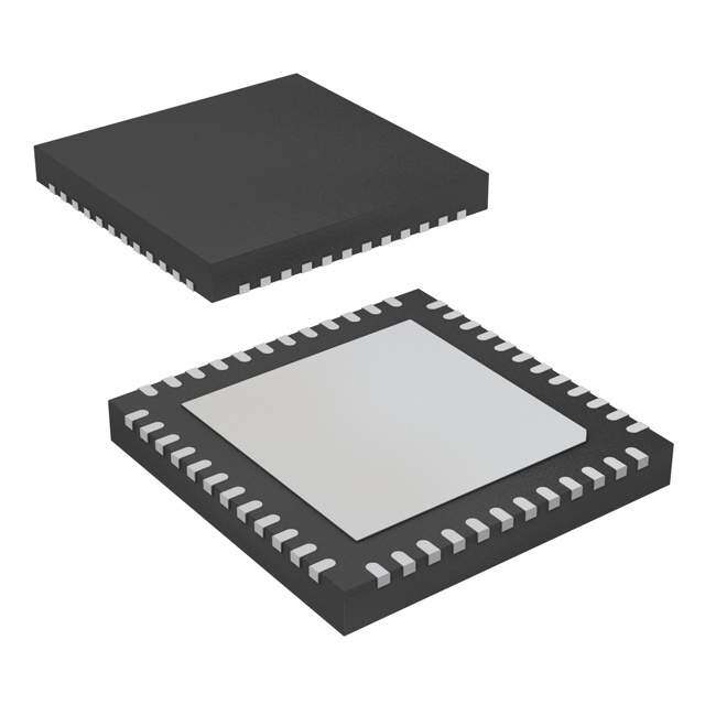
| 描述 | IC POWER/BATTERY MGMT 48-QFN电池管理 Li-Ion Powered Systems |
| 产品分类 | |
| 品牌 | Texas Instruments |
| 产品手册 | |
| 产品图片 |
|
| rohs | 符合RoHS无铅 / 符合限制有害物质指令(RoHS)规范要求 |
| 产品系列 | 电源管理 IC,电池管理,Texas Instruments TPS65014RGZT- |
| 数据手册 | |
| 产品型号 | TPS65014RGZT |
| PCN封装 | |
| 产品目录页面 | |
| 产品种类 | 电池管理 |
| 供应商器件封装 | 48-VQFN(7x7) |
| 其它名称 | 296-17695-6 |
| 功能 | |
| 包装 | Digi-Reel® |
| 单位重量 | 140 mg |
| 商标 | Texas Instruments |
| 安装类型 | 表面贴装 |
| 安装风格 | SMD/SMT |
| 封装 | Reel |
| 封装/外壳 | 48-VFQFN 裸露焊盘 |
| 封装/箱体 | VQFN-48 |
| 工作温度 | -40°C ~ 85°C |
| 工作电源电压 | 4.5 V to 6.5 V |
| 工厂包装数量 | 250 |
| 最大工作温度 | + 85 C |
| 最小工作温度 | - 40 C |
| 标准包装 | 1 |
| 电压-电源 | 4.5 V ~ 6.5 V |
| 电池化学 | 锂离子,锂聚合物 |
| 电池类型 | Li-Ion, Li-Poly |
| 系列 | TPS65014 |
| 输出电压 | 4.2 V |
| 输出电流 | 1000 mA |


- 商务部:美国ITC正式对集成电路等产品启动337调查
- 曝三星4nm工艺存在良率问题 高通将骁龙8 Gen1或转产台积电
- 太阳诱电将投资9.5亿元在常州建新厂生产MLCC 预计2023年完工
- 英特尔发布欧洲新工厂建设计划 深化IDM 2.0 战略
- 台积电先进制程称霸业界 有大客户加持明年业绩稳了
- 达到5530亿美元!SIA预计今年全球半导体销售额将创下新高
- 英特尔拟将自动驾驶子公司Mobileye上市 估值或超500亿美元
- 三星加码芯片和SET,合并消费电子和移动部门,撤换高东真等 CEO
- 三星电子宣布重大人事变动 还合并消费电子和移动部门
- 海关总署:前11个月进口集成电路产品价值2.52万亿元 增长14.8%


PDF Datasheet 数据手册内容提取
Product Sample & Technical Tools & Support & Folder Buy Documents Software Community TPS65014 SLVS551A–DECEMBER2004–REVISEDSEPTEMBER2015 TPS65014 Power- and Battery-Management IC for Li-Ion Powered Systems 1 Features 3 Description • LinearChargerManagementforSingleLi-Ionor The TPS65014 device is an integrated power- and 1 battery-management IC for applications powered by Li-PolymerCells one Li-ion or Li-polymer cell and which require • DualInputPortsforChargingFromUSBorFrom multiple power rails. The TPS65014 provides two WallPlug,Handles100-mAand500-mAUSB highly efficient, step-down converters targeted at Requirements providingthecorevoltageandperipheralI/Orailsina • ChargeCurrentProgrammableThroughExternal processor-based system. Both step-down converters Resistor enter a low-power mode at light load for maximum efficiency across the widest possible range of load • 1-A,95%EfficientStep-DownConverterforI/O currents. The LOW_PWR pin allows the core andPeripheralComponents(VMAIN) converter to lower its output voltage when the • 400-mA,90%EfficientStep-DownConverterfor application processor goes into deep sleep. The ProcessorCore(VCORE) TPS65014 also integrates two 200-mA LDO voltage • 2× 200-mALDOsforI/OandPeripheral regulators, which are enabled through the serial interface. Each LDO operates with an input voltage Components,LDOEnableThroughBus range of 1.8 V to 6.5 V, thus allowing them to be • SerialInterfaceCompatibleWithI2C,Supports supplied from one of the step-down converters or 100-kHz,400-kHzOperation directlyfromthebattery. • LOW_PWRPintoLowerorDisableProcessor CoreSupplyVoltageinDeep-SleepMode DeviceInformation(1) • 70-µAQuiescentCurrent PARTNUMBER PACKAGE BODYSIZE(NOM) • 1%ReferenceVoltage TPS65014 VQFN(48) 7.00mm×7.00mm • Thermal-ShutdownProtection (1) For all available packages, see the orderable addendum at theendofthedatasheet. 2 Applications FunctionalBlockDiagram • AllSingleLi-IonCell-OperatedProductsRequiring MultipleSuppliesIncluding: MAX(AC,USB,VBAT) AC – PDAs USB VBAT – CellularandSmartPhones PG – InternetAudioPlayers Linear Charge Controller – DigitalStillCameras ISTEST AGND2 • DigitalRadioPlayers • Split-SupplyDSPandµPSolutions SSCDLAKT InSteerrfiaacle Thermal IFLSB Shutdown VINMAIN PS_SEQ LOW_PWR VMAIN L1 PB_ONOFF VMAIN BHATOTT__CROEVSEERT Control SCtoepn-vDeortwern DPGEFNMDA1IN TPOR RESPWRON MPU_RESET VCC AGND3 INT VINCORE L2 UVLO VCORE PWRFAIL VORSECF SCtoepn-vDeortwern VDCEOFCROERE GPIO1 PGND2 GGGPPPIIIOOO234 GPIOs VINLDO1 VIB VLDO1 VLDO1 200-mALDO VFB_LDO1 LED2 AGND1 VINLDO2 VLDO2 VLDO2 200-mALDO 1 An IMPORTANT NOTICE at the end of this data sheet addresses availability, warranty, changes, use in safety-critical applications, intellectualpropertymattersandotherimportantdisclaimers.PRODUCTIONDATA.
TPS65014 SLVS551A–DECEMBER2004–REVISEDSEPTEMBER2015 www.ti.com Table of Contents 1 Features.................................................................. 1 7.3 FeatureDescription.................................................20 2 Applications........................................................... 1 7.4 DeviceFunctionalModes........................................37 3 Description............................................................. 1 7.5 RegisterMaps.........................................................38 4 RevisionHistory..................................................... 2 8 ApplicationandImplementation........................ 51 8.1 ApplicationInformation............................................51 5 PinConfigurationandFunctions......................... 3 8.2 TypicalApplication .................................................51 6 Specifications......................................................... 5 9 PowerSupplyRecommendations...................... 56 6.1 AbsoluteMaximumRatings......................................5 9.1 BatteryCharger.......................................................56 6.2 ESDRatings..............................................................5 9.2 LDO1OutputVoltageAdjustment...........................59 6.3 RecommendedOperatingConditions.......................5 10 Layout................................................................... 59 6.4 ThermalInformation..................................................6 6.5 ElectricalCharacteristics...........................................6 10.1 LayoutGuidelines.................................................59 6.6 ElectricalCharacteristics:BatteryCharger...............9 10.2 LayoutExample....................................................60 6.7 DissipationRatings.................................................11 11 DeviceandDocumentationSupport................. 61 6.8 SerialInterfaceTimingRequirements.....................12 11.1 DeviceSupport......................................................61 6.9 SwitchingCharacteristics........................................12 11.2 CommunityResources..........................................61 6.10 TypicalCharacteristics..........................................13 11.3 Trademarks...........................................................61 7 DetailedDescription............................................ 18 11.4 ElectrostaticDischargeCaution............................61 7.1 Overview.................................................................18 11.5 Glossary................................................................61 7.2 FunctionalBlockDiagram.......................................19 12 Mechanical,Packaging,andOrderable Information........................................................... 61 4 Revision History NOTE:Pagenumbersforpreviousrevisionsmaydifferfrompagenumbersinthecurrentversion. ChangesfromOriginal(December2004)toRevisionA Page • AddedESDRatingstable,FeatureDescriptionsection,DeviceFunctionalModes,ApplicationandImplementation section,PowerSupplyRecommendationssection,Layoutsection,DeviceandDocumentationSupportsection,and Mechanical,Packaging,andOrderableInformationsection. ................................................................................................ 1 2 SubmitDocumentationFeedback Copyright©2004–2015,TexasInstrumentsIncorporated ProductFolderLinks:TPS65014
TPS65014 www.ti.com SLVS551A–DECEMBER2004–REVISEDSEPTEMBER2015 5 Pin Configuration and Functions RGZPackage 48-PinVQFN TopView NET ET R OS S W L RE E P AI WR R OW_ T WRF ESPPU_ OT_CLKDATLSB POR PIO1PIO2 L IN P RM HSSIF T GG 36 35 3433 3231 30 29 28 2726 25 ISET 37 24 VLDO1 TS 38 23 VFB_LDO1 BATT_COVER 39 22 VINLDO1 AC 40 21 AGND1 VBAT_A 41 20 VLDO2 VBAT_B 42 19 VINLDO2 USB 43 18 GPIO3 AGND2 44 17 GPIO4 AGND3 45 16 PGND1_B PGND2 46 15 PGND1_A PB_ONOFF 47 14 PS_SEQ VCORE 48 13 VMAIN 1 2 3 4 5 6 7 8 9 1011 12 E2 B 2EC ABAB GN FCORLED VI LNCORVC MAIN_MAIN_L1_L1_ PEFMAI E VI NN D D VIVI NC−No internal connection PinFunctions PIN I/O DESCRIPTION NAME NO. CHARGERSECTION ChargerinputvoltagefromACadapter.TheACpincanbeleftopenorcanbeconnectedto AC 40 I groundifthechargerisnotused. AGND2 44 — Analoggroundconnection.Allanaloggroundpinsareconnectedinternallyonthechip. ISET 37 I ExternalchargecurrentsettingresistorconnectionforusewithACadapter PG 11 O Indicateswhenavalidpowersupplyispresentforthecharger(open-drain) TS 38 I Batterytemperaturesenseinput ChargerinputvoltagefromUSBport.TheUSBpincanbeleftopenorcanbeconnectedto USB 43 I groundifthechargerisnotused. VBAT_A 41 I Senseinputforthebatteryvoltage.Connectdirectlywiththebattery. VBAT_B 42 O Poweroutputofthebatterycharger.Connectdirectlywiththebattery. ThermalPad — — ConnectthethermalpadtoGND SWITCHINGREGULATORSECTION AGND3 45 — Analoggroundconnection.Allanaloggroundpinsareconnectedinternallyonthechip. L1_A,L1_B 9,10 — SwitchpinofVMAINconverter.TheVMAINinductorisconnectedhere. L2 4 — SwitchpinofVCOREconverter.TheVCOREinductorisconnectedhere. PGND1_A, 15,16 — PowergroundforVMAINconverter PGND1_B PGND2 46 — PowergroundforVCOREconverter Copyright©2004–2015,TexasInstrumentsIncorporated SubmitDocumentationFeedback 3 ProductFolderLinks:TPS65014
TPS65014 SLVS551A–DECEMBER2004–REVISEDSEPTEMBER2015 www.ti.com PinFunctions(continued) PIN I/O DESCRIPTION NAME NO. SWITCHINGREGULATORSECTION(continued) PowersupplyfordigitalandanalogcircuitryofMAINandCOREDC-DCconverters.This VCC 6 I mustbeconnectedtothesamevoltagesupplyasVINCOREandVINMAIN.Alsosupplies serialinterfaceblock VCORE 48 I VCOREfeedbackvoltagesenseinput,connectdirectlytoVCORE VMAIN 13 I VMAINfeedbackvoltagesenseinput,connectdirectlytoVMAIN VINMAIN_A, InputvoltageforVMAINstep-downconverter.Thismustbeconnectedtothesamevoltage 7,8 I VINMAIN_B supplyasVINCOREandVCC. InputvoltageforVCOREstep-downconverter.Thismustbeconnectedtothesamevoltage VINCORE 5 I supplyasVINMAINandVCC. LDOREGULATORSECTION AGND1 21 — Analoggroundconnection.Allanaloggroundpinsareconnectedinternallyonthechip. VFB_LDO1 23 I FeedbackinputfromexternalresistivedividerforLDO1 VINLDO1 22 I InputvoltageforLDO1 VINLDO2 19 I InputvoltageforLDO2 VLDO1 24 O OutputvoltageforLDO1 VLDO2 20 O OutputandfeedbackvoltageforLDO2 DRIVERSECTION LED2 2 O LEDdriver,withblinkrateprogrammablethroughtheserialinterface VIB 3 O Vibratordriver,enabledthroughtheserialinterface CONTROLANDI2CSECTION BATT_COVER 39 I Indicatesifbatterycoverisinplace DEFCORE 1 I InputsignalindicatingdefaultVCOREvoltage,0=1.5V,1=1.8V DEFMAIN 12 I InputsignalindicatingdefaultVMAINvoltage,0=3V,1=3.3V GPIO1 26 I/O General-purposeopen-draininput/output GPIO2 25 I/O General-purposeopen-draininput/output GPIO3 18 I/O General-purposeopen-draininput/output GPIO4 17 I/O General-purposeopen-draininput/output HOT_RESET 31 I Push-buttonresetinputusedtorebootorwakeupprocessorthroughtheTPS65014 IFLSB 28 I LSBofserialinterfaceaddressusedtodistinguishtwodeviceswiththesameaddress Indicatesachargefaultortermination,orifanyoftheregulatoroutputsarebelowthelower INT 35 O tolerancelevel,activelow(open-drain) LOW_PWR 36 I Inputsignalindicatingdeepsleepmode,VCOREisloweredtopredefinedvalueordisabled MPU_RESET 32 O Open-drainresetoutputgeneratedbyuseractivatedHOT_RESET PB_ONOFF 47 I Push-buttonenablepin,alsousedtowakeupprocessorfromlowpowermode PS_SEQ 14 I Setspower-up/downsequenceofstep-downconverters Open-drainoutput.ActivelowwhenUVLOcomparatorindicateslowVBATconditionorwhen PWRFAIL 34 O shutdownisabouttooccurduetoanovertemperatureconditionorwhenthebatterycoveris removed(BATT_COVERhasgonelow). Open-drainsystemresetoutput,generatedaccordingtothestateoftheVMAINoutput RESPWRON 33 O voltage.Ifthemainoutputisdisabled,RESPWRONisactive(inotherwords,low). SCLK 30 I Serialinterfaceclockline SDAT 29 I/O Serialinterfacedata/address SetstheresetdelaytimeatRESPWRON.TPOR=0:T =100ms. TPOR 27 I n(RESPWRON) TPOR=1:T =1s. n(RESPWRON) 4 SubmitDocumentationFeedback Copyright©2004–2015,TexasInstrumentsIncorporated ProductFolderLinks:TPS65014
TPS65014 www.ti.com SLVS551A–DECEMBER2004–REVISEDSEPTEMBER2015 6 Specifications 6.1 Absolute Maximum Ratings overoperatingfree-airtemperaturerangeunlessotherwisenoted(1) MIN MAX UNIT InputvoltageonVACpinwithrespecttoAGND 20 V InputvoltagerangeonallotherpinsexceptAGND/PGNDpinswithrespectto –0.3 7 V AGND CurrentatAC,VBAT,VINMAIN,L1,PGND1 1800 mA Peakcurrentatallotherpins 1000 mA SeeDissipation Continuouspowerdissipation Ratings Operatingfree-airtemperature,T –40 85 °C A Maximumjunctiontemperature,T 125 °C J Storagetemperature,T –65 150 °C stg Leadtemperature1,6mm(1/16inch)fromcasefor10seconds 260 °C (1) StressesbeyondthoselistedunderAbsoluteMaximumRatingsmaycausepermanentdamagetothedevice.Thesearestressratings only,andfunctionaloperationofthedeviceattheseoranyotherconditionsbeyondthoseindicatedunderRecommendedOperating Conditionsisnotimplied.Exposuretoabsolute-maximum-ratedconditionsforextendedperiodsmayaffectdevicereliability. 6.2 ESD Ratings VALUE UNIT Human-bodymodel(HBM),perANSI/ESDA/JEDECJS-001(1)(2) ±1000 V(ESD) Electrostaticdischarge Charged-devicemodel(CDM),perJEDECspecificationJESD22- V C101(3)(2) ±1000 (1) JEDECdocumentJEP155statesthat500-VHBMallowssafemanufacturingwithastandardESDcontrolprocess.Manufacturingwith lessthan500-VHBMispossiblewiththenecessaryprecautions.Pinslistedas±1000Vmayactuallyhavehigherperformance. (2) AtpinsVIB,PG,andLED2 (3) JEDECdocumentJEP157statesthat250-VCDMallowssafemanufacturingwithastandardESDcontrolprocess.Manufacturingwith lessthan250-VCDMispossiblewiththenecessaryprecautions.Pinslistedas±1000Vmayactuallyhavehigherperformance. 6.3 Recommended Operating Conditions MIN NOM MAX UNIT V SupplyvoltagefromACadapter 4.5 6.5 V (AC) V SupplyvoltagefromUSB 4.4 5.25 V (USB) V Voltageatbattery 2.5 4.2 V (BAT) V ,V V Inputvoltagerangestep-downconverters 2.5 6.0 V I(MAIN) I(CORE), CC V ,V InputvoltagerangeforLDOs 1.8 6.5 V I(LDO1) I(LDO2) T Operatingambienttemperature -40 85 °C A T Operatingjunctiontemperature -40 125 °C J ResistorfromV ),V toV usedfor R I(main I(core) CC 10 100 Ω (CC) filtering,C =1µF I(VCC) Copyright©2004–2015,TexasInstrumentsIncorporated SubmitDocumentationFeedback 5 ProductFolderLinks:TPS65014
TPS65014 SLVS551A–DECEMBER2004–REVISEDSEPTEMBER2015 www.ti.com 6.4 Thermal Information TPS65014 THERMALMETRIC(1) RGZ(VQFN) UNIT 48PINS R Junction-to-ambientthermalresistance 27.0 °C/W θJA R Junction-to-case(top)thermalresistance 14.3 °C/W θJC(top) R Junction-to-boardthermalresistance 4.6 °C/W θJB ψ Junction-to-topcharacterizationparameter 0.2 °C/W JT ψ Junction-to-boardcharacterizationparameter 4.6 °C/W JB R Junction-to-case(bottom)thermalresistance 1.1 °C/W θJC(bot) (1) Formoreinformationabouttraditionalandnewthermalmetrics,seetheSemiconductorandICPackageThermalMetricsapplication report,SPRA953. 6.5 Electrical Characteristics V =V =V =V =V =3.6V,T =–40°Cto85°C,typicalvaluesareatT =25°Cbatterycharger I(MAIN) I(CORE) CC I(LDO1) I(LDO2) A A specificationsarevalidintherange0°C<T <85°Cunlessotherwisenoted A PARAMETER TESTCONDITIONS MIN TYP MAX UNIT CONTROLSIGNALS:LOW_PWR,SCLK,SDAT(INPUT) VIH High-levelinputvoltage IIH=20µA(1) 2 VCC V VIL Low-levelinputvoltage IIL=10µA 0 0.8 V IIB Inputbiascurrent 0.01 1 µA CONTROLSIGNALS:PB_ONOFF,HOT_RESET,BATT_COVER VIH High-levelinputvoltage IIH=20µA(1) 0.8VCC 6 V VIL Low-levelinputvoltage IIL=10µA 0 0.4 V R(pb_onoff) PulldownresistoratPB_ONOFF 1000 kΩ PullupresistoratHOT_RESET, R(hot_reset) connectedtoVCC 1000 kΩ R(batt_cover) PulldownresistoratBATT_COVER 2000 kΩ CONTROLSIGNALS:MPU_RESET,PWRFAIL,RESPWRON,INT,SDAT(OUTPUT) VOH High-leveloutputvoltage 6 V VOL Low-leveloutputvoltage IIL=10mA 0 0.3 V SUPPLYPIN:VCC I(Q) Operatingquiescentcurrent VI=3.6V,currentintoMain+Core+VCC 70 µA IO(SD) Shutdownsupplycurrent VCIu=rre3n.6tiVn,toBMATaTin_+COCVorEeR+=VGCCND, 15 25 µA (1) IftheinputvoltageishigherthanV ,anadditionalinputcurrent,limitedbyaninternal10-kΩresister,flows. CC 6 SubmitDocumentationFeedback Copyright©2004–2015,TexasInstrumentsIncorporated ProductFolderLinks:TPS65014
TPS65014 www.ti.com SLVS551A–DECEMBER2004–REVISEDSEPTEMBER2015 Electrical Characteristics (continued) V =V =V =V =V =3.6V,T =–40°Cto85°C,typicalvaluesareatT =25°Cbatterycharger I(MAIN) I(CORE) CC I(LDO1) I(LDO2) A A specificationsarevalidintherange0°C<T <85°Cunlessotherwisenoted A PARAMETER TESTCONDITIONS MIN TYP MAX UNIT VMAINSTEP-DOWNCONVERTER VI Inputvoltagerange 2.5 6 V IO Maximumoutputcurrent 1000 mA IO(SD) Shutdownsupplycurrent BATT_COVER=GND 0.1 1 µA rDS(on) P-channelMOSFETon-resistance VI(MAIN)=VGS=3.6V 110 210 mΩ Ilkg(p) P-channelleakagecurrent V(DS)=6V 1 µA rDS(on) N-channelMOSFETon-resistance VI(MAIN)=VGS=3.6V 110 200 mΩ Ilkg(N) N-channelleakagecurrent V(DS)=6V 1 µA IL P-channelcurrentlimit 2.5V<VI(MAIN)<6V 1.4 1.75 2.1 A fS Oscillatorfrequency 1 1.25 1.5 MHz VI(MAIN)=2.7Vto6V;IO=0mA 0% 3% 2.5V VI(MAIN)=2.7Vto6V; 3% 3% 0mA≤IO≤1000mA VI(MAIN)=2.95Vto6V;IO=0mA 0% 3% 2.75V VI(MAIN)=2.95Vto6V; 3% 3% 0mA≤IO≤1000mA VO(MAIN) Fixedoutputvoltage VI(MAIN)=3.2Vto6V;IO=0mA 0% 3% 3.0V VI(MAIN)=3.2Vto6V; 3% 3% 0mA≤IO≤1000mA VI(MAIN)=3.5Vto6V;IO=0mA 0% 3% 3.3V VI(MAIN)=3.5Vto6V; 3% 3% 0mA≤IO≤1000mA Lineregulation VI(MAIN)=VO(MAIN)+0.5V(min.2.5V)to6V, 0.5 %/V IO=10mA Loadregulation IO=10mAto1000mA 0.12 %/A R(VMAIN) VMAINdischargeresistance 400 Ω VCORESTEP-DOWNCONVERTER VI Inputvoltagerange 2.5 6 V IO Maximumoutputcurrent 400 mA IO(SD) Shutdownsupplycurrent BATT_COVER=GND 0.1 1 µA rDS(on) P-channelMOSFETon-resistance VI(CORE)=VGS=3.6V 275 530 mΩ Ilkg(p) P-channelleakagecurrent VDS=6V 0.1 1 µA rDS(on) N-channelMOSFETon-resistance VI(CORE)=VGS=3.6V 275 500 mΩ Ilkg(N) N-channelleakagecurrent VDS=6V 0.1 1 µA IL P-channelcurrentlimit 2.5V<VI(CORE)<6V 600 700 900 mA fS Oscillatorfrequency 1 1.25 1.5 MHz Copyright©2004–2015,TexasInstrumentsIncorporated SubmitDocumentationFeedback 7 ProductFolderLinks:TPS65014
TPS65014 SLVS551A–DECEMBER2004–REVISEDSEPTEMBER2015 www.ti.com Electrical Characteristics (continued) V =V =V =V =V =3.6V,T =–40°Cto85°C,typicalvaluesareatT =25°Cbatterycharger I(MAIN) I(CORE) CC I(LDO1) I(LDO2) A A specificationsarevalidintherange0°C<T <85°Cunlessotherwisenoted A PARAMETER TESTCONDITIONS MIN TYP MAX UNIT VCORESTEP-DOWNCONVERTER(continued) VI(CORE)=2.5Vto6V; 0% 3% IO=0mA,CO =22µF 0.85V VI(CORE)=2.5Vto6V; 3% 3% 0mA≤IO≤400mA,CO=22µF VI(CORE)=2.5Vto6V; 0% 3% IO=0mA,CO =22µF 1.0V VI(CORE)=2.5Vto6V; 3% 3% 0mA≤IO≤400mA,CO=22µF VI(CORE)=2.5Vto6V; 0% 3% IO=0mA,CO =22µF 1.1V VI(CORE)=2.5Vto6V; 3% 3% 0mA≤IO≤400mA,CO =22µF VI(CORE)=2.5Vto0V;IO =0mA 0% 3% 1.2V VO(CORE) Fixedoutputvoltage VI(CORE)=2.5Vto6V;0mA≤IO≤400mA 3% 3% VI(CORE)=2.5Vto6V;IO=0mA 0% 3% 1.3V VI(CORE)=2.5Vto6V; 3% 3% 0mA≤IO≤400mA VI(CORE)=2.5Vto6V;IO=0mA 0% 3% 1.4V VI(CORE)=2.5Vto6V; 3% 3% 0mA≤IO≤400mA VI(CORE)=2.5Vto6V;IO=0mA 0% 3% 1.5V VI(CORE)=2.5Vto6V; 3% 3% 0mA≤IO≤400mA VI(CORE)=2.5Vto6V;IO=0mA 0% 3% 1.8V VI(CORE)=2.5Vto6V; 3% 3% 0mA≤IO≤400mA Lineregulation VI(CORE)=VO(MAIN)+0.5V 1 %/V (min.2.5V)to6V,IO=10mA Loadregulation IO=10mAto400mA 0.002 %/mA R(VCORE) VCOREdischargeresistance 400 Ω VLDO1andVLDO2LOW-DROPOUTREGULATORS LD01 1.8 6.5 VI Inputvoltagerange V LD02 1.8 VCC VO LDO1outputvoltagerange 0.9 VINLDO1 V Vref Referencevoltage 485 500 515 mV VO LDO2outputvoltagerange 1.8 3.3 V Full-powermode 200 IO Maximumoutputcurrent mA Low-powermode 30 LDO1andLDO2short-circuitcurrent I(SC) limit VLDO1=GND,VLDO2=GND 650 mA Dropoutvoltage IO=200mA,VINLDO1,2=1.8V 300 mV Totalaccuracy ±3% VINLDO1,2=VLDO1,2+0.5V Lineregulation 0.75 %/V (min.2.5V)to6.5V,IO =10mA Loadregulation IO =10mAto200mA 0.011 %/mA Loadchangefrom10%to90% 0.1 Regulationtime ms Low-powermode 0.1 I(QFP) LDOquiescentcurrent(eachLDO) Full-powermode 16 30 µA I(QLPM) LDOquiescentcurrent(eachLDO) Low-powermode 12 18 µA IO(SD) LDOshutdowncurrent(eachLDO) 0.1 1 µA Ilkg(FB) Leakagecurrentfeedback 0.01 0.1 µA 8 SubmitDocumentationFeedback Copyright©2004–2015,TexasInstrumentsIncorporated ProductFolderLinks:TPS65014
TPS65014 www.ti.com SLVS551A–DECEMBER2004–REVISEDSEPTEMBER2015 6.6 Electrical Characteristics: Battery Charger V +V ≤V =V orV ,I <I ≤1A,0°C<T <85°C O(REG) (DO-MAX) (CHG) (AC) (USB) (TERM) O A PARAMETER TESTCONDITIONS MIN TYP MAX UNIT VLDO1andVLDO2LOW-DROPOUTREGULATORS(continued) V(AC) Inputvoltagerange 4.5 6.5 V V(USB) Inputvoltagerange 4.35 5.25 V ICC(VCHG) Supplycurrent V(CHG)>V(CHG)min 1.2 2 mA SumofcurrentsintoVBATpin, ICC(SLP) Sleepcurrent V(CHG)<V(SLP-ENTRY), 2 5 µA 0°C≤TJ≤85°C CurrentintoUSBpin 45 ICC(STBY) Standbycurrent µA CurrentintoACpin 200 400 VOLTAGEREGULATOR VO Outputvoltage V(CHG)min≥4.5V 4.15 4.20 4.25 V Dropoutvoltage(V(AC)–VBAT) VIOO(O(RUETG))=+1VA(DO-MAX)≤V(CHG), 500 800 VDO Dropoutvoltage(V(USB)–VBAT) VIOO(O(RUETG))=+0V.5(DAO-MAX)≤V(CHG), 300 500 mV Dropoutvoltage(V(USB)–VBAT) VIOO(O(RUETG))=+0V.1(DAO-MAX)≤V(CHG), 100 150 CURRENTREGULATION IO(AC) Outputcurrentrangeforacoperation(1) VVC(AHCG)-≥V4I(.B5ATV)>,VVI((ODOUT-M)A>X)V(LOWV), 100 1000 mA Outputcurrentsetvoltageforacoperation atISETpin.100%outputcurrentI2C 2.45 2.50 2.55 registerCHGCONFIG<4:3>=11 75%outputcurrentI2Cregister V(SET) C50H%GCouOtpNuFtIGcu<r4re:3n>tI=2C10register VVmI(BinAT≥)4>.5V(VDO,-VMIA(BXA)T)>V(LOWV),V(AC)- 1.83 1.91 1.99 V 1.23 1.31 1.39 CHGCONFIG<4:3>=01 32%outputcurrentI2Cregister 0.76 0.81 0.86 CHGCONFIG<4:3>=00 100mA<IO<1000mA 310 330 350 KSET Outputcurrentsetfactorforacoperation 10mA<IO<100mA 300 340 380 V(CHG)min≥4.35V,VI(BAT)>V(LOWV), V(USB)-VI(BAT)>V(DO-MAX), 80 100 I2CregisterCHGCONFIG<2>=0 IO(USB) OutputcurrentrangeforUSBoperation mA V(CHG)min≥4.5V,VI(BAT) >V(LOWV), VUSB-VI(BAT)>V(DO-MAX), 400 500 I2CregisterCHGCONFIG<2>=1 R(ISET) ResistorrangeatISETpin 825 8250 Ω PRECHARGECURRENTREGULATION,SHORT-CIRCUITCURRENT,ANDBATTERYDETECTIONCURRENT Prechargetofast-chargetransition V(LOWV) threshold, V(CHG)min≥4.5V 2.8 3 3.2 V voltageonVBATpin. I(PRECHG) Prechargecurrent(2) 0≤VI(OUT)<V(LOWV),t<t(PRECHG) 10 100 mA I(DETECT) Batterydetectioncurrent 200 µA V(SET-PRECHG) VoltageatISETpin 0≤VI(OUT)<V(LOWV),t<t(PRECHG) 240 255 270 mV KSET × V (SET) I = O(AC) R (1) (ISET) KSET × V (SET_PRECHG) I = (PRECHG) R (2) (ISET) Copyright©2004–2015,TexasInstrumentsIncorporated SubmitDocumentationFeedback 9 ProductFolderLinks:TPS65014
TPS65014 SLVS551A–DECEMBER2004–REVISEDSEPTEMBER2015 www.ti.com Electrical Characteristics: Battery Charger (continued) V +V ≤V =V orV ,I <I ≤1A,0°C<T <85°C O(REG) (DO-MAX) (CHG) (AC) (USB) (TERM) O A PARAMETER TESTCONDITIONS MIN TYP MAX UNIT CHARGETAPERANDTERMINATIONDETECTION I(TAPER) Tapercurrentdetectrange(3) VI(OUT)>V(RCH),t<t(TAPER) 10 100 mA VoltageatISETpinforchargeTAPER V(SET_TAPER) detection VI(OUT)>V(RCH),t<t(TAPER) 235 250 265 mV VoltageatISETpinforchargertermination V(SET_TERM) detection(4) VI(OUT)>V(RCH) 11 18 25 mV TEMPERATURECOMPARATOR V(LTF) Low(cold)temperaturethreshold 2.475 2.50 2.525 V V(HTF) High(hot)temperaturethreshold 0.485 0.5 0.515 V I(TS) TScurrentsource 95 102 110 µA BATTERYRECHARGETHRESHOLD V(RCH) Rechargethreshold V(CHG)min≥4.5V VO(R0E.1G1)–5 VO(REG0).–1 VO(R0E.0G8)–5 V SLEEPANDSTANDBY Sleep-modeentrythreshold, V(CHG)≤ V(SLP-ENTRY) PGoutput=high 2.3V≤VI(OUT)≤VO(REG) VI(OUT) V +150mV Sleep-modeexitthreshold, V(CHG)≥ V(SLP_EXIT) PGoutput=low 2.3V≤VI(OUT)≤VO(REG) VI(OUT)+ V 250mV CHARGERPOWER-ON-RESET,UVLO,ANDV(IN)RAMPRATE V(CHGUVLO) Chargerundervoltagelockout V(CHG)decreasing 2.27 2.5 2.75 V Hysteresis 27 mV V(CHGOVLO) Chargerovervoltagelockout 6.5 V CHARGEROVERTEMPERATURESUSPEND Temperatureatwhichchargersuspends T(suspend) operation 145 °C T(hyst) Hysteresisofsuspendthreshold 20 °C KSET × V (SET_TAPER) I = (TAPER) R (3) (ISET) KSET × V (SET_TERM) I = (TERM) R (4) (ISET) 10 SubmitDocumentationFeedback Copyright©2004–2015,TexasInstrumentsIncorporated ProductFolderLinks:TPS65014
TPS65014 www.ti.com SLVS551A–DECEMBER2004–REVISEDSEPTEMBER2015 Electrical Characteristics: Battery Charger (continued) V +V ≤V =V orV ,I <I ≤1A,0°C<T <85°C O(REG) (DO-MAX) (CHG) (AC) (USB) (TERM) O A PARAMETER TESTCONDITIONS MIN TYP MAX UNIT LOGICSIGNALSDEFMAIN,DEFCORE,PS_SEQ,IFLSB VIH High-levelinputvoltage IIH=20µA VCC–0.5 VCC V VIL Low-levelinputvoltage IIL=10µA 0 0.4 V IIB Inputbiascurrent 0.01 1 µA LOGICSIGNALSGPIO1-4 VOL Low-leveloutputvoltage IoOpLe=n-1drmaiAn,ocuotnpfuigturedasan 0.3 V VOH High-leveloutputvoltage Configuredasanopen-drainoutput 6 V VIL Low-levelinputvoltage 0 0.8 V VIH High-levelinputvoltage 2 VCC(5) V II Inputleakagecurrent 1 µA rDS(on) InternalNMOS VOL=0.3V 150 Ω LOGICSIGNALSPG,LED2 VOL Low-leveloutputvoltage IOL=20mA 0.5 V VOH High-leveloutputvoltage 6 V V(PG) PGthresholdvoltageUSBandAC V(BAT)+mxVx V VIBRATORDRIVERVIB VOL Low-leveloutputvoltage IOL=100mA 0.3 0.5 V VOH High-leveloutputvoltage 6 V THERMALSHUTDOWN T(SD) Thermalshutdown Increasingjunctiontemperature 160 °C UNDERVOLTAGELOCKOUT V(UVLO)2.5V -3% 3% Undervoltagelockout threshold. V(UVLO)2.75V Filterresistor=10Rinseries -3% 3% V(UVLO) TUhVeLOdeifsau2l.t7v5aVluefor V(UVLO)3.0V withVCC,VCCdecreasing -3% 3% V(UVLO)3.25V -3% 3% V(UVLO_HYST) UVLOcomparatorhysteresis VCCrising 350 400 450 mV POWERGOOD VMAIN,VCORE,VLDO1,VLDO2 Decreasingrailvoltage –12% –10% –8% decreasing VMAIN,VCORE,VLDO1,VLDO2 Increasingrailvoltage –7% –5% –3% increasing (5) IftheinputvoltageishigherthanV anadditionalcurrentflows,limitedbyaninternal10-kΩresistor. CC 6.7 Dissipation Ratings See (1) AMBIENT MAXPOWERDISSIPATION DERATINGFACTOR TEMPERATURE FORT =125°C(2) ABOVET =55°C j A 25°C 3W 30mW/°C 55°C 2.1W (1) TheTPS65014ishousedina48-pinQFNpackagewithexposedleadframeontheunderside.This7-mm×7-mmpackageexhibitsa thermalimpedance(junction-to-ambient)of33K/WwhenmountedonaJEDEChigh-kboard. (2) Considerationneedstobegiventothemaximumchargecurrentwhentheassembledapplicationboardexhibitsathermalimpedance whichdifferssignificantlyfromtheJEDEChigh-kboard. Copyright©2004–2015,TexasInstrumentsIncorporated SubmitDocumentationFeedback 11 ProductFolderLinks:TPS65014
TPS65014 SLVS551A–DECEMBER2004–REVISEDSEPTEMBER2015 www.ti.com 6.8 Serial Interface Timing Requirements MIN MAX UNIT Clockfrequency,f 400 kHz MAX Clockhightime,t 600 ns wH(HIGH) Clocklowtime,t 1300 ns wL(LOW) DATAandCLKrisetime,t 300 ns R DATAandCLKfalltime,t 300 ns F Holdtime(repeated)STARTcondition(afterthisperiodthefirstclockpulseisgenerated),t 600 ns h(STA) SetuptimeforrepeatedSTARTcondition,t 600 ns h(DATA) Datainputholdtime,t 0 ns h(DATA) Datainputsetuptime,t 100 ns su(DATA) STOPconditionsetuptime,t 600 ns su(STO) Busfreetime,t 1300 ns (BUF) 6.9 Switching Characteristics overoperatingfree-airtemperaturerange(unlessotherwisenoted) PARAMETER TESTCONDITIONS MIN TYP MAX UNIT CONTROLSIGNALS:PB_ONOFF,HOT_RESET,BATT_COVER t Deglitchtimeatall3pins 38 56 77 ms (glitch) Delayaftert (PWRFAILgoes (glitch) t low)beforesuppliesaredisabled 1.68 2.4 3.2 ms (batt_cover) whenBATT_COVERgoeslow. CONTROLSIGNALS:MPU_RESET,PWRFAIL,RESPWRON,INT,SDAT(OUTPUT) Durationoflowpulseat t 100 µs d(mpu_nreset) MPU_RESET Durationoflowpulseat TPOR=0 80 100 120 t RESPWRONafterVMAINisin ms d(nrespwron) regulation TPOR=1 800 1000 1200 TimebetweenUVLOgoingactive t (PWRFAILgoinglow)andsupplies 1.68 2.4 3.2 ms d(uvlo) beingdisabled Timebetweenchip overtemperatureconditionbeing t 1.68 2.4 3.2 ms d(overtemp) recognized(PWRFAILgoinglow) andsuppliesbeingdisabled PRECHARGECURRENTREGULATION,SHORT-CIRCUITCURRENT,ANDBATTERYDETECTIONCURRENT V min≥4.5V,V (CHG) I(OUT) Deglitchtime decreasingbelowthreshold;100-ns 8.8 23 60 ms falltime,10-mVoverdrive CHARGETAPERANDTERMINATIONDETECTION V min≥4.5V,chargingcurrent (CHG) increasingordecreasingaboveand DeglitchtimeforI 8.8 23 60 ms (TAPER) below;100-nsfalltime,10-mV overdrive V min≥4.5V,chargingcurrent (CHG) DeglitchtimeforI decreasingbelow;100-nsfalltime, 8.8 23 60 ms (TERM) 10-mVoverdrive TEMPERATURECOMPARATOR Deglitchtimefortemperaturefault 8.8 23 60 ms BATTERYRECHARGETHRESHOLD V min≥4.5V,V (CHG) I(OUT) decreasingbelowthreshold;100-ns Deglitchtime 8.8 23 60 ms falltime, 10-mVoverdrive 12 SubmitDocumentationFeedback Copyright©2004–2015,TexasInstrumentsIncorporated ProductFolderLinks:TPS65014
TPS65014 www.ti.com SLVS551A–DECEMBER2004–REVISEDSEPTEMBER2015 Switching Characteristics (continued) overoperatingfree-airtemperaturerange(unlessotherwisenoted) PARAMETER TESTCONDITIONS MIN TYP MAX UNIT TIMERS t Prechargetimer V min≥4.5V 1500 1800 2160 s (PRECHG) (CHG) t Tapertimer V min≥4.5V 1500 1800 2160 s (TAPER) (CHG) t Chargetimer V min≥4.5V 15000 18000 21600 s (CHG) (CHG) SLEEPANDSTANDBY ACorUSBdecreasingbelow Deglitchtimeforsleepmodeentry threshold;100-nsfalltime,10-mV 8.8 23 60 ms andexit overdrive DelaybetweenvalidUSBvoltage t beingappliedandstartofcharging 5 ms (USB_DEL) processfromUSB 6.10 Typical Characteristics Table1.TableofGraphs FIGURE Figure1, Efficiency vsOutputcurrent Figure2 Quiescentcurrent vsInputvoltage Figure3 Switchingfrequency vsTemperature Figure4 Figure5- LDO1Outputvoltage vsOutputcurrent Figure8 LDO2Outputvoltage vsOutputcurrent Figure9 Linetransientresponse(main) Figure9 Linetransientresponse(core) Figure10 Linetransientresponse(LDO1) Figure11 Linetransientresponse(LDO2) Figure12 Loadtransientresponse(main) Figure13 Loadtransientresponse(core) Figure14 Loadtransientresponse(LDO1) Figure15 Loadtransientresponse(LDO2) Figure16 Outputvoltageripple(PFM) Figure17 Outputvoltageripple(PWM) Figure18 Start-uptiming Figure19 Figure20, Dropoutvoltage vsOutputcurrent Figure21 PSRR(LDO1andLDO2) vsFrequency Figure22 Copyright©2004–2015,TexasInstrumentsIncorporated SubmitDocumentationFeedback 13 ProductFolderLinks:TPS65014
TPS65014 SLVS551A–DECEMBER2004–REVISEDSEPTEMBER2015 www.ti.com 100 100 Main: Core: VO=1.6V 90 VI=3.8V, 90 VI=3.8V, 80 TA=25°C, 80 TA=25°C, PFWM=1 PFWM=1 70 70 −% 60 VO=3.3V VO=2.5V −% 60 VO=1.2V y y nc 50 nc 50 Efficie 40 Efficie 40 VO=0.85V 30 30 20 20 10 10 0 0 0.01 0.10 1 10 100 1k 10k 0.01 0.10 1 10 100 1k IO−Output Current−mA IO−Output Current−mA Figure1.EfficiencyvsOutputCurrent Figure2.EfficiencyvsOutputCurrent 70 1.230 VCC,+Vcore,+Vmain VI=4.2V mA 60 TA=85°C Hz 1.225 Current - 4500 TA=-40°C uency - M 11..221250 VI=3.3V scent 30 TA=25°C g Freq 1.210 e n ui hi Q 20 c 1.205 wit S 10 f - 1.200 0 1.195 2.5 3 3.5 4 4.5 5 5.5 6 -40-30-20-10 0 10 20 30 40 50 60 708085 VI- Input Voltage - V TA- Free-Air Temperature -°C Figure3.QuiescentCurrentvsInputVoltage Figure4.SwitchingFrequencyvsTemperature 3.401 1.652 TA=25°C TA=25°C 3.381 1.642 V V ge− 3.361 VI=6V ge−1.632 VI=3.3V oltaV 3.341 VI=5V oltaV1.622 VI=3.6V ut 3.321 ut 1.612 p p Out 3.301 Out1.602 VI=4.2V 1 1 O 3.281 O1.592 D D L L −O3.261 VI=4.2V −O1.582 V V 3.241 VI=3.6V 1.572 VI=5V 3.221 VI=3.3V 1.562 VI=6V 3.201 1.552 0 10 100 1k 10k 100k 0 10 100 1k 10k 100k IOOutput Current−mA IOOutput Current−mA Figure5.LD01OutputVoltagevsOutputCurrent Figure6.LD01OutputVoltagevsOutputCurrent 14 SubmitDocumentationFeedback Copyright©2004–2015,TexasInstrumentsIncorporated ProductFolderLinks:TPS65014
TPS65014 www.ti.com SLVS551A–DECEMBER2004–REVISEDSEPTEMBER2015 3 3.1 2.90 V VO=2.8V 2.9 VO=3V e - 2.80 oltagV 2.70 ge - V 2.7 Output 22..5600 VO=2.5V oltaut V 2.5 VTAOL=D2O5°2C=3.8V O1 2.40 utp 2.3 D O - LVO 22..2300 LDO2 2.1 2.10 VTAIL=D2O51°C=3.8V V- O 1.9 VO=1.8V 2 1.7 0.01 0.1 1 10 100 1000 0.01 0.1 1 10 100 1000 IOOutput Current - mA IO- Output Current - mA Figure7.LDO1OutputVoltagevsOutputCurrent Figure8.LDO2OutputVoltagevsOutputCurrent VI=3.6Vto4.2V,VO=1.6V, CH1=VI mV/div IL=400mA,TA=25°C CH1=VI mV/div 500 500 VI=3.6 to4.2V,VO=3.3V, IL=500mATA=25°C CH2=VO v CH2=VO v di di V/ V/ m m 0 0 5 5 500 µs/div 500 µs/div Figure9.LineTransientResponse(Main) Figure10.LineTransientResponse(Core) VI=3.3 to3.8V,VO=2.8V, VI=3.3 to3.8V,VO=1.8V, IL=100mA,TA=25°C RL=100mAto1000mA, TA=25°C div CH1=VI CH1=VI mV/ v 0 V/di 50 m 0 0 5 v CH2=VO div CH2=VO mV/di mV/ 10 0 1 500 µs/div 500 µs/div Figure11.LineTransientResponse(LDO1) Figure12.LineTransientResponse(LDO2) Copyright©2004–2015,TexasInstrumentsIncorporated SubmitDocumentationFeedback 15 ProductFolderLinks:TPS65014
TPS65014 SLVS551A–DECEMBER2004–REVISEDSEPTEMBER2015 www.ti.com CH4=IO VI=3.8V,VO=1.6V, IL=40mAto400mA, mA/div TA=25°C CH4=IO A/div m 0 0 0 VI=3.8V,VO=3.3V, 5 50 IL=100mAto1000mA, TA=25°C CH2=VO v CH2=VO div di V/ V/ m m 0 00 10 2 100 µs/div 100 µs/div Figure13.LoadTransientResponse(Main) Figure14.LoadTransientResponse(Core) VI=3.8V,VILDO=3.3V, VO=1.8V,IL=2mAto180mA, CH4=IO A/div TA=25°C A/div m m 200 CH4=IO 200 VI=3.8V,VILDO=3.3V, VO= 2.8V,IL=2mAto180mA, TA=25°C CH2=VO div CH2=VO div V/ V/ m m 0 0 0 0 1 1 100 µs/div 100 µs/div Figure15.LoadTransientResponse(LDO1) Figure16.LoadTransientResponse(LDO2) mV/div mV/div CH1 = VOMain 50 CH3=IinductorMain CH1 = VOMain 20 CH3= Iinductor Main div A/div mA/ m 00 0 1 0 2 div CH2 = VOCore div CH2 = VOCore V/ V/ m m 50 CH4=IinductorCore div 20 CH4=IinductorCore A/div A/ m m 0 00 10 5 ms/div 1 500 ns/div VI=3.8V,TA=25°C VI=3.8V,TA=25°C VOMain= 3.3VILMain=100mA, VOMain= 3.3VRLMain=500mA, VOCore=1.6V,ILCore=40mA VOCore=1.6V,RLCore=400mA Figure17.OutputRipple(PFM) Figure18.OutputRipple(PWM) 16 SubmitDocumentationFeedback Copyright©2004–2015,TexasInstrumentsIncorporated ProductFolderLinks:TPS65014
TPS65014 www.ti.com SLVS551A–DECEMBER2004–REVISEDSEPTEMBER2015 0.25 CH1=VOMain LDO1VO=2.5V 0.2 CH3=IcoilMain LDO2VO=1.8V V e - 0.15 LDO2VO=3V g CH2=VOCore olta V CH4=IcoilCore opout 0.1 LDO1VO=2.8V Dr 0.05 NormalMode TA=25°C 0 500 ms/div 0 20 40 60 80 100120140160180200 VI=3.8V,VOMain= 3.3V, IO- Output Current - mA RLMain=1A,VOCore=1.6V, RLCore=400mA,TA=25°C Figure19.Start-UpTiming Figure20.DropoutVoltagevsOutputCurrent 0.05 80 0.045 70 LDOIN=3.3V 0.04 LDO2VO=1.8V LDO Output Current 10 mA V 60 e - 0.035 LDO2VO=3V ag 0.03 B 50 oltut V0.025 LDO1VO=2.8V RR-d 40 po 0.02 PS o 30 Dr0.015 LDO1VO=2.5V 20 LDO Output Current 200 mA 0.01 LowPowerMode 0.005 10 TA=25°C 0 0 0 3 6 9 12 15 18 21 24 27 30 1k 10k 100k 1M 10M IO- Output Current - mA f - Frequency - Hz Figure21.DropoutVoltagevsOutputCurrent Figure22.PSRR(LDO1,LDO2)vsFrequency Copyright©2004–2015,TexasInstrumentsIncorporated SubmitDocumentationFeedback 17 ProductFolderLinks:TPS65014
TPS65014 SLVS551A–DECEMBER2004–REVISEDSEPTEMBER2015 www.ti.com 7 Detailed Description 7.1 Overview TheTPS65014hasahighlyintegratedandflexibleLi-Ionlinearchargerandsystempowermanagement.Itoffers an integrated USB port and AC-adapter supply management with autonomous power-source selection, power FETandcurrentsensor,highaccuracycurrentandvoltageregulation,chargestatus,andchargetermination. The TPS65014 charger automatically selects the USB port or the AC adapter as the power source for the system. In the USB configuration, the host can increase the charge current from the default value of maximum 100mA to 500 mA through the interface. In the AC adapter configuration, an external resistor sets the maximum valueofchargecurrent. The battery is charged in three phases: conditioning, constant current, and constant voltage. Charge is normally terminated based on minimum current. An internal charge timer provides a safety backup for charge termination. The TPS65014 automatically restarts the charge if the battery voltage falls below an internal threshold. The chargerautomaticallyenterssleepmodewhenbothsuppliesareremoved. The serial interface can be used for dynamic voltage scaling, for collecting information on and controlling the battery charger status, for optionally controlling 2-LED driver outputs, a vibrator driver, masking interrupts, or for disabling, enabling, and setting the LDO output voltages. The interface is compatible with the fast- and standard- modeI2Cspecification,thusallowingtransfersupto400kHz. 18 SubmitDocumentationFeedback Copyright©2004–2015,TexasInstrumentsIncorporated ProductFolderLinks:TPS65014
TPS65014 www.ti.com SLVS551A–DECEMBER2004–REVISEDSEPTEMBER2015 7.2 Functional Block Diagram MAX(AC,USB,VBAT) AC USB VBAT PG Linear Charge Controller ISET AGND2 TS SCLK Serial SDAT Interface Thermal Shutdown IFLSB VINMAIN PS_SEQ LOW_PWR VMAIN L1 PB_ONOFF VMAIN BATT_COVER Step-Down DEFMAIN Converter HOT_RESET Control PGND1 TPOR RESPWRON VCC MPU_RESET AGND3 INT VINCORE L2 UVLO VCORE PWRFAIL VREF VCORE OSC Step-Down DEFCORE Converter GPIO1 PGND2 GPIO2 GPIOs GPIO3 VINLDO1 GPIO4 VIB VLDO1 VLDO1 200-mALDO VFB_LDO1 LED2 AGND1 VINLDO2 VLDO2 VLDO2 200-mALDO Copyright©2004–2015,TexasInstrumentsIncorporated SubmitDocumentationFeedback 19 ProductFolderLinks:TPS65014
TPS65014 SLVS551A–DECEMBER2004–REVISEDSEPTEMBER2015 www.ti.com 7.3 Feature Description 7.3.1 Step-DownConverters,VMAINandVCORE The TPS65014 incorporates two synchronous step-down converters operating typically at 1.25-MHz fixed frequency pulse width modulation (PWM) at moderate to heavy load currents. At light load currents, the converters automatically enter power-save mode and operate with pulse frequency modulation (PFM). The main converteriscapableofdelivering1-Aoutputcurrentandthecoreconverteriscapableofdelivering400mA. The converter output voltages are programmed through the VDCDC1 and VDCDC2 registers in the serial interface. The main converter defaults to 3-V or 3.3-V output voltage depending on the DEFMAIN configuration pin, if DEFMAIN is tied to ground, the default is 3 V; if it is tied to V , the default is 3.3 V. The core converter CC defaults to either 1.5 V or 1.8 V, depending on whether the DEFCORE configuration pin is tied to GND or to V , CC respectively. Both the main and core output voltages can subsequently be reprogrammed after start-up through the serial interface. In addition, the LOW_PWR pin can be used either to lower the core voltage to a value defined in the VDCDC2 register when the application processor is in deep sleep mode, or to disable the core converter.AnactivesignalatLOW_PWRisignorediftheENABLE_LPbitisnotsetintheVDCDC1register. The step-down converter outputs (when enabled) are monitored by power-good comparators, the outputs of which are available through the serial interface. The outputs of the DC-DC converters can be optionally dischargedwhentheDC-DCconvertersaredisabled. During PWM operation, the converters use a fast response voltage-mode controller scheme with input voltage feed-forward to achieve good line and load regulation, allowing the use of small ceramic input and output capacitors. At the beginning of each clock cycle, initiated by the clock signal, the P-channel MOSFET switch is turned on, and the inductor current ramps up until the comparator trips and the control logic turns off the switch. The current limit comparator also turns off the switch if the current limit of the P-channel switch is exceeded. After the dead time preventing current shoot through, the N-channel MOSFET rectifier is turned on, and the inductor current ramps down. The next cycle is initiated by the clock signal, again turning off the N-channel rectifierandturningontheP-channelswitch. The error amplifier, together with the input voltage, determines the rise time of the saw-tooth generator, and therefore any change in input voltage or output voltage directly controls the duty cycle of the converter, giving a goodlineandloadtransientregulation. The two DC-DC converters operate synchronized to each other, with the MAIN converter as the master. A 270° phase shift between the MAIN switch turnon and the CORE switch turnon decreases the input RMS current, and smaller input capacitors can be used. This is optimized for a typical application where the MAIN converter regulatesaLi-ionbatteryvoltageof3.7Vto3.3VandtheCOREfrom3.7Vto1.5V. 7.3.1.1 ForcedPWM The core and main converters are forced into PWM mode by setting bit 7 in the VDCDC1 register. This feature is usedtominimizerippleontheoutputvoltages. 7.3.1.2 DynamicVoltagePositioning As described in the power-save mode operation sections and as detailed in Figure 11, the output voltage is typically 1.2% above the nominal output voltage at light load currents, as the device is in power-save mode. This gives additional headroom for the voltage drop during a load transient from light load to full load. During a load transient from full load to light load, the voltage overshoot is also minimized due to active regulation turning on theN-channelrectifierswitch. 7.3.1.3 Soft-Start Both converters have an internal soft-start circuit that limits the inrush current during start-up. The soft start is implemented as a digital circuit, increasing the switch current in 4 steps up to the typical maximum switch current limit of 700 mA (core) and 1.75 A (main). Therefore, the start-up time mainly depends on the output capacitor andloadcurrent. 20 SubmitDocumentationFeedback Copyright©2004–2015,TexasInstrumentsIncorporated ProductFolderLinks:TPS65014
TPS65014 www.ti.com SLVS551A–DECEMBER2004–REVISEDSEPTEMBER2015 Feature Description (continued) 7.3.1.4 100%DutyCycleLowDropoutOperation The TPS65014 converters offer a low input to output voltage difference while maintaining operation with the use of the 100% duty cycle mode. In this mode, the P-channel switch is constantly turned on. This is particularly useful in battery-powered applications to achieve longest operation time by taking full advantage of the whole battery voltage range. The minimum input voltage to maintain regulation depends on the load current and output voltageandiscalculatedinEquation1: (cid:4) (cid:5) VI(min)(cid:3)VO(max)(cid:2)IO(max)(cid:1) rDS(on)max(cid:2)RL where • I =maximumoutputcurrentplusinductorripplecurrent O(max) • r =maximumP-channelswitchr DS(on)max DSon • R =DCresistanceoftheinductor L • V =nominaloutputvoltageplusmaximumoutputvoltagetolerance (1) O(max) 7.3.1.5 ActiveDischargeWhenDisabled When the CORE and MAIN converters are disabled, due to an UVLO, BATT_COVER, or OVERTEMP condition, it is possible to actively pull down the outputs. This feature is disabled per default and is individually enabled through the VDCDC1 and VDCDC2 registers in the serial interface. When this feature is enabled, the core and mainoutputsaredischargedbya400-Ω (typical)load. 7.3.1.6 Power-GoodMonitoring Both the MAIN and CORE converters have power-good comparators. Each comparator indicates when the relevant output voltage has dropped 10% below its target value, with 5% hysteresis. The outputs of these comparators are available in the REGSTATUS register through the serial interface. A maskable interrupt is generated when any voltage rail drops below the 10% threshold. The comparators are disabled when the converters are disabled. The status of the power-good comparator for VMAIN is used to generate the RESPWRONsignal. 7.3.1.7 OvertemperatureShutdown The MAIN and CORE converters are automatically shut down if the temperature exceeds the trip point (see Electrical Characteristics). This detection is only active if the converters are in PWM mode, either by setting FPWM=1,oriftheoutputcurrentishighenoughthatthedevicerunsinPWMmodeautomatically. 7.3.2 Low-DropoutVoltageRegulators The low-dropout voltage regulators are designed to operate with low value ceramic input and output capacitors. They operate with input voltages down to 1.8 V. The LDOs offer a maximum dropout voltage of 300 mV at rated output current. Each LDO has a current limit feature. Both LDOs are enabled per default; both LDOs can be disabled or programmed through the serial interface using the VREGS1 register. The LDO outputs (when enabled) are monitored by power-good comparators, the outputs of which are available through the serial interface. The LDOs also have reverse conduction prevention when disabled. This allows the possibility to connectexternalregulatorsinparallelinsystemswithabackupbattery. 7.3.2.1 Power-GoodMonitoring Both the LDO1 and LDO2 linear regulators have power-good comparators. Each comparator indicates when the relevant output voltage has dropped 10% below its target value, with 5% hysteresis. The outputs of these comparators are available in the REGSTATUS register through the serial interface. An interrupt is generated whenanyvoltageraildropsbelowthe10%threshold.TheLDO2comparatorisdisabledwhenLDO2isdisabled. Copyright©2004–2015,TexasInstrumentsIncorporated SubmitDocumentationFeedback 21 ProductFolderLinks:TPS65014
TPS65014 SLVS551A–DECEMBER2004–REVISEDSEPTEMBER2015 www.ti.com Feature Description (continued) 7.3.2.2 EnablingandSequencing Enabling and sequencing of the DC-DC converters and LDOs are described in the power-up sequencing section. The OMAP1510 processor from Texas Instruments requires that the core power supply is enabled before the I/O power supply, which means that the CORE converter should power up before the MAIN converter. This is achievedbyconnectingPS_SEQtoGND. 7.3.3 UndervoltageLockout The undervoltage lockout circuit for the four regulators on TPS65014 prevents the device from malfunctioning at low input voltages and from excessive discharge of the battery. Basically, it prevents the converter from turning on the power switch or rectifier FET under undefined conditions. The undervoltage threshold voltage is set by default to 2.75 V. After power up, the threshold voltage can be reprogrammed through the serial interface. The undervoltage lockout comparator compares the voltage on the VCC pin with the UVLO threshold. When the VCC voltage drops below this threshold, the TPS65014 sets the PWRFAIL pin low and after a time t disables the (UVLO) voltage regulators in the sequence defined by PS_SEQ. The same procedure is followed when the TPS65014 detects that its junction temperature has exceeded the overtemperature threshold, typically 160°C, with a delay t . The TPS65014 automatically restarts when the UVLO (or overtemperature) condition is no longer (overtemp) present. The battery charger circuit has a separate UVLO circuit with a threshold of typically 2.5 V, which is compared withthevoltageonACandUSBsupplypins. 7.3.4 Power-UpSequencing The TPS65014 power-up sequencing is designed to allow the maximum flexibility without generating excessive logisticalorsystemcomplexity.TherelevantcontrolpinsaredescribedinTable2. 22 SubmitDocumentationFeedback Copyright©2004–2015,TexasInstrumentsIncorporated ProductFolderLinks:TPS65014
TPS65014 www.ti.com SLVS551A–DECEMBER2004–REVISEDSEPTEMBER2015 Feature Description (continued) Table2.ControlPins PINNAME INPUT/OUTPUT FUNCTION Inputsignalindicatingpower-upandpower-downsequenceoftheswitchingconverters.PS_SEQ=0 PS_SEQ I forcesthecoreregulatortorampupfirstanddownlast.PS_SEQ=1forcesthemainregulatortorampup firstanddownlast. DefinesthedefaultvoltageoftheVCOREswitchingconverter.DEFCORE=0defaultsVCOREto1.5V, DEFCORE I DEFCORE=VCCdefaultsVCOREto1.8V. DefinesthedefaultvoltageoftheVMAINswitchingconverter.DEFMAIN=0defaultsVMAINto3V, DEFMAIN I DEFMAIN=VCCdefaultsVMAINto3.3V. TheLOW_PWRpinisusedtolowerVCOREtothepresetvoltageintheVDCDC2registerwhenthe processorisindeepsleepmode.Alternatively,VCOREcanbedisabledinlowpowermodeifthe LP_COREOFFbitissetintheVDCDC2register.LOW_PWRisignorediftheENABLELPbitisnotsetin theVDCDC1register.TheTPS65014usestherisingedgeoftheinternalsignalformedbyalogicalAND ofLOW_PWRandENABLELPtoenterlowpowermode.TPS65014isforcedoutoflowpowermodeby LOW_PWR I deassertingLOW_PWR,byresettingENABLELPto0,byactivatingthePB_ONOFFpinorbyactivating theHOT_RESETpin.Therearetwowaystogetthedevicebackintolowpowermode:a)togglethe LOW_PWRpin,orb)togglethelowpowerbitwhentheLOW_PWRpinisheldhigh.TheLOW_PWRpin isalsousedtosettheTPS65014intoWAITmode.IfUSBorACispresent,theAUAbit(CHCONFIG<7>) mustbesettoentertheWAITmode,seeFigure23. PB_ONOFFcanbeusedtoexitthelowpowermodeandreturnthecorevoltagetothevaluebeforelow powermodewasentered.IfPB_ONOFFisusedtoexitthelowpowermode,thenthelowpowermode PB_ONOFF I canbereenteredbytogglingtheLOW_PWRpinorbytogglingthelowpowerbitwhentheLOW_PWRpin isheldhigh.A1-MΩpulldownresistorisintegratedinTPS65014.PB_ONOFFisinternallyde-bouncedby theTPS65014.AmaskableinterruptisgeneratedwhenPB_ONOFFisactivated. TheHOT_RESETpinhasasimilarfunctionalitytothePB_ONOFFpin.Inaddition,itgeneratesareset (MPU_RESET)fortheMPUwhentheVCOREvoltageisinregulation.HOT_RESETdoesnotalterany HOT_RESET I TPS65014settingsunlesslowpowermodewasactiveinwhichcaseitisexited.A1-MΩpullupresistorto VCCisintegratedinTPS65014.HOT_RESETisinternallyde-bouncedbytheTPS65014. TheBATT_COVERpinisusedasanearlywarningthatthemainbatteryisabouttoberemoved. BATT_COVER=VCCindicatesthatthecoverisinplace,BATT_COVER=0indicatesthatthecoverisnot inplace.TPS65014generatesamaskableinterruptwhentheBATT_COVERpingoeslow.PWRFAILis BATT_COVER I alsoheldlowwhenBATT_COVERgoeslow.ThisfeaturemaybedisabledbytyingBATT_COVER permanentlytoVCC.TheTPS65014shutsdownthemainandthecoreconverterandsetstheLDOsinto lowpowermode.A2-MΩpulldownresistorisintegratedintheTPS65014attheBATT_COVERpin. BATT_COVERisinternallyde-bouncedbytheTPS65014. RESPWRONisheldlowwhiletheswitchingconverters(andanyLDOsdefinedasdefaulton)arestarting up.ItisdeterminedbythestateofMAIN'soutputvoltage;whenthevoltageishigherthanthepower-good RESPWRON O comparatorthreshold;thenRESPWRONishighwhenVMAINislow;thenRESPWRONislow. RESPWRONisheldlowfortn(RESPWRON)secondsafterVMAINhassettled. MPU_RESETcanbeusedtoresettheprocessoriftheuseractivatestheHOT_RESETbutton.The MPU_RESET O MPU_RESEToutputisactivefort(MPU_nRESET)sec.ItalsoforcesTPS65014toleavelowpowermode. MPU_RESETisalsoheldlowaslongasRESPWRONisheldlow. PWRFAILindicateswhenVCC<V(UVLO),whentheTPS65014isabouttoshutdownduetoaninternal PWRFAIL O overtemperatureconditionorwhenBATT_COVERislow.PWRFAILisalsoheldlowaslongas RESPWRONisheldlow. TPORisusedtosetthedelaytimefortheRESPWRONresetsignal. TPOR I TPOR=0setsthedelaytimeto100ms.TPOR=1setsthedelaytimeto1s. Copyright©2004–2015,TexasInstrumentsIncorporated SubmitDocumentationFeedback 23 ProductFolderLinks:TPS65014
TPS65014 SLVS551A–DECEMBER2004–REVISEDSEPTEMBER2015 www.ti.com Figure 23 shows the state diagram for TPS65014 power sequencing. The charger function is not shown in the statediagrambecausethisfunctionisindependentofthesestates. No MonitoredPermanently Power TPS65011 ACand/orUSB MainBatteryPower VVoMltAaIgNe No PRWERSFPAWILR,O INNT,, PowerApplied. Applied Enabledand MPU_RESETLow. Good? Reset RESPWRONTimer MonitoredPermanently Yes Yes VCC>UVOL, BTAjT<HTTs_ighChtOd?wVnE,R W∗A1IT TimeRrEiSfSNPtoWatrRtROunNning No No ACand/orUSB PowerApplied SetPWRFAILLow, or RESPWRON StartUVLO_TEMP No PB_ONOFF or TimerDone? TimerifNotRunning HOT_RESET No ButtonPressed. Yes VCC>UVLO? VCC>UVLO? Release UTiVmLeOr_DToEnMeP? BATHT_igChO?VER No BATHT_igChO?VER PRWERSFPAWILR,O INNT,, MPU_RESET Yes Value Yes PS_SEQ? 1 0 BootVCORE BootVMAIN ShutdownVCORE, Converter+LDOs Converter+LDOs Yes VMAIN+LDOs Accordingto PS_SEQ BootVCORE BootVCORE Converter Converter LOW_PWR De-asserted, PB_ONOFF ButtonPressed ProScheusstdoorwInnit∗ia3ted ON ALOssWer_tePdW∗R2 PLOOWWE_R Mode HOT_RESET ButtonPressed ∗1:AllregistersareresettotheirdefaultvaluesinWAITMode ∗2:ENABLE_LPbit,VDCDC1<3>Mustbeset. No IfACorUSBpowerispresent,AUAbit,CHGCONFIG<7>mustalsobeset. Raisethelowpowerpintoenterlowpowermode. ∗3:EENNAABBLLEE__LSPUbPitP,LVYDbCitD,VCD1C<D3>C1m<u4s>tbmeussettb.ecleared. MPRUe_leRaEsSeET VCOGRoEodVo?ltage LDO2OFF/SLPand LDO1OFF/SLP<6,2>mustbesetorLDOsandvoltage referenceremainenabledandregistersnotreset. Yes Yes IfACorUSBpowerispresent,AUAbit,CHGCONFIG<7>mustalsobeset. Raisethelowpowerpintoenterlowpowermode. SetMPU_RESET ENABLE_LPdefault:cleared MPU_RESET Low,Start ENABLE_SUPPLYdefault:set TimerDone? MPU_RESETTimer AUAdefault:cleared LDO1OFF/SLPdefault:cleared No LDO2OFF/SLPdefault:cleared Figure23. TPS65014Power-OnStateDiagram 24 SubmitDocumentationFeedback Copyright©2004–2015,TexasInstrumentsIncorporated ProductFolderLinks:TPS65014
TPS65014 www.ti.com SLVS551A–DECEMBER2004–REVISEDSEPTEMBER2015 7.3.4.1 TPS65014PowerStateDescriptions 7.3.4.1.1 State1:NoPower No batteries are connected to the TPS65014. When main power is applied, the bandgap reference, LDOs, and UVLO comparator start up. The RESPWRON, PWRFAIL, INT, and MPU_RESET signals are held low. When BATT_COVER goes high (de-bounced internally by the TPS65014), indicating that the battery cover has been put in place and if VCC > UVLO, the power supplies are ramped in the sequence defined by PS_SEQ. RESPWRON, PWRFAIL, INT, and MPU_RESET are released when the RESPWRON timer has timed out after t seconds. If VCC remains valid and no OVERTEMP condition occurs, then the TPS65014 arrives in n(RESPWRON) State 2: ON. If VCC < UVLO, the TPS65014 keeps the bandgap reference and UVLO comparator active such thatwhenVCC>UVLO(duringbatterycharge),thesuppliesareautomaticallyactivated. 7.3.4.1.2 State2:ON In this state, the TPS65014 is fired up and ready for operation. The switching converter output voltages can be programmed. The LDOs can be disabled or programmed. The TPS65014 can exit this state due to an overtemperature condition, an undervoltage condition at VCC, BATT_COVER going low, or by the processor programminglowpowermode.State2islefttemporarilyiftheuseractivatesthe HOT_RESET pin. 7.3.4.1.3 State3:Low-PowerMode This state is entered through the processor setting the ENABLE_LP bit in the serial interface and then raising the LOW_PWR pin. The TPS65014 uses the rising edge of the internal signal formed by a logical AND of the LOW_PWR and ENABLE LP signals to enter low power mode. The VMAIN switching converter remains active, but the VCORE converter may be disabled in low power mode through the serial interface by setting the LP_COREOFF bit in the VDCDC2 register. If left enabled, the VCORE voltage is set to the value predefined by the CORELP0/1 bits in the VDCDC2 register. The LDO1OFF/nSLP and LDO2OFF/nSLP bits in the VREGS1 register determine whether the LDOs are turned off or put in a reduced power mode (transient speed-up circuitry disabled in order to minimize quiescent current) in low power mode. All TPS65014 features remain addressable through the serial interface. The TPS65014 can exit this state either due to an undervoltage condition at VCC, due to BATT_COVER going low, due to an OVERTEMP condition, by the processor deasserting the LOW_POWERpin,orbytheuseractivatingthe HOT_RESET pinorthePB_ONOFFpin. 7.3.4.1.4 State4:Shutdown There are two scenarios for entering this state. The first is from State 1: No Power. As soon as main battery powerisapplied,thedeviceautomaticallyenterstheWAITmode. The second scenario occurs when the device is in ON mode and the processor initiates a shutdown by resetting the ENABLE SUPPLY bit in the VDCDC1 register (ENABLE_LP must be high), and then raising the LOW_PWR pin. When this happens, the power rails are ramped down in the predefined sequence, and all circuitry is then disabled. In this state, the TPS65014 waits for the PB_ONOFF or HOT_RESET pin to be activated before enabling any of the supply rails. When the PB_ONOFF or HOT_RESET pin is activated, the TPS65014 powers up the supplies according to the same constraints as at the initial application of power. Complete shutdown is only achieved by setting the LDO1OFF/nSLP and LDO2OFF/nSLP bits high in the VREGS1 register before activatingtheshutdown. In this case, the I2C interface is deactivated, and the registers are reset to their default value after leaving the WAITmode. To enter the WAIT mode when USB or AC is present, set the AUA bit (CHCONFIG<7>). The WAIT mode is automatically left if bit 7 in register CHCONFIG is set to 0 (default), and a voltage is present at either the AC pin or the USB pin in the appropriate range for charging, and the voltage at V is above the UVLO threshold. This CC featureallowstheconverterstostartupautomaticallyifthedeviceispluggedinforcharging. If all supplies are turned off in WAIT mode, the internal bandgap is switched off, and the internal registers are resettotheirdefaultstatewhenthedevicereturnstoONmode. Table3listspossibleconfigurationsinLOWPOWERmodeandWAITmode. Copyright©2004–2015,TexasInstrumentsIncorporated SubmitDocumentationFeedback 25 ProductFolderLinks:TPS65014
TPS65014 SLVS551A–DECEMBER2004–REVISEDSEPTEMBER2015 www.ti.com Table3.TPS65014PossibleConfigurations(1) CONVERTER MAIN CORE LDO1 LDO2 LOWPOWERmode 1 0/1 0/1 0/1 WAITmode 0 0 0/1 0/1 (1) 0=converterisdisabled 1=converterisenabled Table4indicatesthetypicalquiescent-currentconsumptionineachpowerstate. Table4.TPS65014TypicalCurrentConsumption TOTALQUIESCENT STATE QUIESCENTCURRENTBREAKDOWN CURRENT 1 0 2 30µA–70µA VMAIN(12µA)+VCORE(12µA)+LDOs(20µAeach,max2)+UVLO+reference+ PowerGood 3 30µA–55µA VMAIN(12µA)+VCORE(12µA)+LDOs(10µAeach,max2)+UVLO+reference+ PowerGood 4 13µA UVLO+referencecircuitry 26 SubmitDocumentationFeedback Copyright©2004–2015,TexasInstrumentsIncorporated ProductFolderLinks:TPS65014
TPS65014 www.ti.com SLVS551A–DECEMBER2004–REVISEDSEPTEMBER2015 VCC BATT COVER BATT COVER t(GLITCH) DEG* PB_ONOFF REFSYS t(GLITCH) EN* UVLO* ENABLE SUPPLIES* VCORE 98% VCORE VMAIN 95% VMAIN VLDO1 VLDO2 RESPWRON MPU_RESET tn(RESPWRON) PWREFAIL INT *Internal Signal Note: ValidforLDO1suppliedfromVMAINasdescribedearlierinthisApplicationSection. Figure24. State1toState2Transition(PS_SEQ=0,V >V +HYST) CC UVLO If 2.4 ms after application V is still below the default UVLO threshold (3.15 V for V rising), then start up is as CC CC showninFigure25. Copyright©2004–2015,TexasInstrumentsIncorporated SubmitDocumentationFeedback 27 ProductFolderLinks:TPS65014
TPS65014 SLVS551A–DECEMBER2004–REVISEDSEPTEMBER2015 www.ti.com AC (or USB) VCC UVLO Threshold BATT COVER t(GLITCH) BAT COVER DEG * REFSYS EN* UVLO* ENABLE SUPPLIES* VCORE 98% VCORE VMAIN 95% VMAIN VLDO1 VLDO2 RESPWRON MPU_RESET PWRFAIL tn(RESPWRON) INT * Internal Signal Note: ValidforLDO1suppliedfromVMAINasdescribedearlierinthisApplicationSection Figure25. State1toState4toState2Transition(Power-UpBehaviorWhenChargeVoltageisApplied) 28 SubmitDocumentationFeedback Copyright©2004–2015,TexasInstrumentsIncorporated ProductFolderLinks:TPS65014
TPS65014 www.ti.com SLVS551A–DECEMBER2004–REVISEDSEPTEMBER2015 VCC UVLO Threshold With 400 mV Hysteresis UVLO* PWPFAIL tUVLO INT ENABLE SUPPLIES* VCORE VMAIN VMAIN ~0.8 V VLDO1 VLDO2 RESPWRON MPU_RESET * Internal Signal Note: ValidforLDO1suppliedfromVMAINasdescribedearlierinthisApplicationSection Figure26. State2toState4Transition Copyright©2004–2015,TexasInstrumentsIncorporated SubmitDocumentationFeedback 29 ProductFolderLinks:TPS65014
TPS65014 SLVS551A–DECEMBER2004–REVISEDSEPTEMBER2015 www.ti.com ENABLE LOW_POWER LDO2 OFF/SLP LOW_POWER VMAIN VCORE 95% VCORE VLDO1 VLDO2 95% VLDO2 INT Note: VCORELowered,LDO2Disabled Note: SubsequentState3toState2TransitionWhenLOWPOWERIsDeasserted. Figure27. State2toState3Transition 30 SubmitDocumentationFeedback Copyright©2004–2015,TexasInstrumentsIncorporated ProductFolderLinks:TPS65014
TPS65014 www.ti.com SLVS551A–DECEMBER2004–REVISEDSEPTEMBER2015 PB_ONOFF PB_ONOFF DEGLITCH tGLITCH VCORE VMAIN VLDO1 VLDO2 INT Note: PB_ONFFActivated(SeeInterruptManagementforINTBehavior) Figure28. State3toState2Transition Copyright©2004–2015,TexasInstrumentsIncorporated SubmitDocumentationFeedback 31 ProductFolderLinks:TPS65014
TPS65014 SLVS551A–DECEMBER2004–REVISEDSEPTEMBER2015 www.ti.com HOT_RESET HOT_RESET DEGLITCH t(GLITCH) VCORE 95% VCORE VMAIN VLDO1 VLDO2 95% VLDO2 INT t(MPU_RESET) MPU_RESET Note: HOT_RESETActivated(SeeInterruptManagementforINTBehavior) Figure29. State3toState2Transition 32 SubmitDocumentationFeedback Copyright©2004–2015,TexasInstrumentsIncorporated ProductFolderLinks:TPS65014
TPS65014 www.ti.com SLVS551A–DECEMBER2004–REVISEDSEPTEMBER2015 ENABLE LOW POWER* LDO1 OFF/SLP* LDO2 OFF/SLP* MAIN DISCHARGE* ENABLE SUPPLY* LOW POWER VMAIN VMAIN < ca 0.8 V VCORE VCORE < ca 0.4 V VLDO1 VLDO2 RESPWRON MPU_RESET PWRFAIL INT REFSYS ENABLE* * Internal Signal Figure30. State1toState4Transition 7.3.5 SystemResetandControlSignals The RESPWRON signal is used as a global reset for the application. It is an open-drain output. The RESPWRON signal is generated according to the power good comparator linked to VMAIN and remains low for t seconds after VMAIN has stabilized. When RESPWRON is low, PWRFAIL, MPU_RESET, and INT n(RESPWRON) arealsoheldlow. If the output voltage of MAIN is less than 90% of its nominal value, as RESPWRON is generated, and if the output voltage of MAIN is programmed to a higher value, which causes the output voltage to fall out of the 90% window,thenaRESPWRONsignalisgenerated. Copyright©2004–2015,TexasInstrumentsIncorporated SubmitDocumentationFeedback 33 ProductFolderLinks:TPS65014
TPS65014 SLVS551A–DECEMBER2004–REVISEDSEPTEMBER2015 www.ti.com The PWRFAIL signal indicates when VCC < UVLO or when the TPS65014 junction temperature has exceeded a reliablevalueorifBATT_COVERistakenlow.Thisopen-drainoutputcanbeconnectedatafastinterruptpinfor immediate attention by the application processor. All supplies are disabled t , t , or t seconds (uvlo) (overtemp) (batt_cover) after PWRFAILhasgonelow,givingtimefortheapplicationprocessortoshutdowncleanly. BATT_COVER is used to detect whether the battery cover is in place or not. If the battery cover is removed, the TPS65014 generates a warning to the processor that the battery is likely to be removed and that it may be prudent to shut down the system. If not required, this feature may be disabled by connecting the BATT_COVER pin to the VCC pin. BATT_COVER is de-bounced internally. Typical de-bounce time is 56 ms. BATT_COVER hasaninternal2-MΩ pulldownresistor. The HOT_RESET input is used to generate an MPU_RESET signal for the application processor. The HOT_RESET pin could be connected to a user-activated button in the application. It can also be used to exit low power mode. In this case, the TPS65014 waits until the VCORE voltage has stabilized before generating the MPU_RESET pulse. The MPU_RESET pulse is active low for t seconds. HOT_RESET has an internal (mpu_nreset) 1-MΩ pullupresistortoV . CC The PB_ONOFF input can be used to exit LOW POWER MODE. It is typically driven by a user-activated pushbutton in the application. Both HOT_RESET and PB_ONOFF are de-bounced internally by the TPS65014. Typicaldebouncetimeis56ms.PB_ONOFFhasaninternal1-MΩ pulldownresistor. PB_ONOFF, BATT_COVER and UVLO events also cause a normal, maskable interrupt to be generated and are notedintheREGSTATUSregister. 7.3.6 VibratorDriver The VIB open-drain output is provided to drive a vibrator motor, controlled through the serial interface register VDCDC2. It has a maximum dropout of 0.5 V at 100-mA load. Typically, an external resistor is required to limit themotorcurrentandafreewheeldiodetolimittheVIBovershootvoltageatturnoff. 7.3.7 LED2Output The LED2 output can be programmed in the same way as the PG output to blink or to be permanently on or off. The LED2_ON and LED2_PER registers are used to control the blink rate. For both PG and LED2, the minimum blink-on time is 10 ms, and this can be increased in 127 10-ms steps to 1280 ms. For both PG and LED2, the minimumblinkperiodis100ms,andthiscanbeincreasedin127100-msstepsto12800ms. 7.3.8 InterruptManagement The open-drain INT pin is used to combine and report all possible conditions through a single pin. Battery and chip temperature faults, precharge timeout, charge timeout, taper timeout, and termination current are each capable of setting INT low, that is, active. INT can also be activated if any of the regulators are below the regulation threshold. Interrupts can also be generated by any of the GPIO pins programmed to be inputs. These inputs can be programmed to generate an interrupt either at the rising or falling edge of the input signal. It is possible to mask an interrupt from any of these conditions individually by setting the appropriate bits in the MASK1, MASK2, or MASK3 registers. By default, all interrupts are masked. Interrupts are stored in the CHGSTATUS, REGSTATUS, and DEFGPIO registers in the serial interface. CHGSTATUS and REGSTATUS interrupts are acknowledged by reading these registers. If a 1 is present in any location, then the TPS65014 automatically sets the corresponding bit in the ACKINT1 or ACKINT2 registers and releases the INT pin. The ACKINT register contents are self-clearing when the condition, which caused the interrupt, is removed. The applicationsprocessorshouldnotnormallyneedtoaccesstheACKINT1orACKINT2registers. Interrupteventsarealwayscaptured;thuswhenaninterruptsourceisunmasked, INT mayimmediatelygoactive due to a previous interrupt condition. This can be prevented by first reading the relevant STATUS register before unmaskingtheinterruptsource. If an interrupt condition occurs, then the INT pin is set low. The CHGSTATUS, REGSTATUS, and DEFGPIO registersshouldberead.Bitpositionscontaininga1(orpossiblya0inDEFGPIO)arenotedbytheCPUandthe corresponding situation resolved. The reading of the CHGSTATUS and REGSTATUS registers automatically acknowledges any interrupt condition in those registers and blocks the path to the INT pin from the relevant bits. No interrupt should be missed during the read process because this process starts by latching the contents of the register before shifting them out at SDAT. Once the contents have been latched (which takes a couple of nanoseconds), the register is free to capture new interrupt conditions. Thus, for practical purposes the probability ofmissinganythingiszero. 34 SubmitDocumentationFeedback Copyright©2004–2015,TexasInstrumentsIncorporated ProductFolderLinks:TPS65014
TPS65014 www.ti.com SLVS551A–DECEMBER2004–REVISEDSEPTEMBER2015 Thefollowingdescribeshowregisters0x01(CHGSTATUS)and0x02(REGSTATUS)arehandled: • CHGSTATUS(5,0)arepositiveedgeset.ReadofsetCHGSTATUS(5,0)bitssetsACKINT1(5,0)bits. • CHGSTATUS(7-6,4-1)arelevelset.ReadofsetCHGSTATUS(7-6,4-1)bitssetsACKINT1(7-6,4-1)bits. • CHGSTATUS(5,0)clearwheninputsignallow,andACKINT1(5,0)bitsarealreadyset. • CHGSTATUS(7-6,4-1)clearwheninputsignalislow. • ACKINT1(7-0)clearwhenCHGSTATUS(7-0)isclear. • REGSTATUS(7-5)arepositiveedgeset.ReadofsetREGSTATUS(7-5)bitssetsACKINT2(7-5)bits. • REGSTATUS(3-0)arelevelset.ReadofsetREGSTATUS(3-0)bitssetsACKINT2(3-0)bits. • REGSTATUS(7-5)clearwheninputsignallow,andACKINT1(7-5)bitarealreadyset. • REGSTATUS(3-0)clearwheninputsignalislow. • ACKINT2(7-0)clearwhenREGSTATUS(7-0)isclear. The following describes the function of the 0x05 (ACKINT1) and 0x06 (ACKINT2) registers. These are not usuallywrittentobytheCPUbecausetheTPS65014internallysets/clearstheseregisters: • ACKINT1(7:0):BitissetwhenthecorrespondingCHGSTATUSsetbitisreadthroughI2C. • ACKINT1(7:0):BitisclearedwhenthecorrespondingCHGSTATUSsetbitclears. • ACKINT2(7:0):BitissetwhenthecorrespondingREGSTATUSsetbitisreadthroughI2C. • ACKINT2(7:0):BitisclearedwhenthecorrespondingREGSTATUSsetbitclears. • ACKINT1(7:0):AbitsetmasksthecorrespondingCHGSTATUSbitfrom INT. • ACKINT2(7:0):AbitsetmasksthecorrespondingREGSTATUSbitfrom INT. Thefollowingdescribesthefunctionofthe0x03(MASK1),0x04(MASK2)and0x0F(MASK3)registers: • MASK1(7:0):AbitsetinthisregistermasksCHGSTATUSfrom INT. • MASK2(7:0):AbitsetinthisregistermasksREGSTATUSfrom INT. • MASK3(7:4):AbitsetinthisregisterdetectsarisingedgeonGPIO. • MASK3(7:4):AbitclearedinthisregisterdetectsafallingedgeonGPIO. • MASK3(3:0):AbitsetinthisregisterclearsGPIODetectsignalfrom INT. GPIO interrupts are located by reading the 0x10 (DEFGPIO) register. The application CPU stores, or can read from DEFGPIO<7:4>, which GPIO is set to input or output. This information together with the information on which edge the interrupt was generated (the CPU either knows this or can read it from MASK3<7:4>) determines whether the CPU is looking for a 0 or a 1 in DEFGPIO<3:0>. A GPIO interrupt is blocked from the INT pin by setting the relevant MASK3<3:0> bit; this must be done by the CPU, there is no auto-acknowledge for the GPIO interrupts. 7.3.9 SerialInterface The serial interface is compatible with the standard and fast mode I2C specifications, allowing transfers at up to 400kHz. The interface adds flexibility to the power supply solution, enabling most functions to be programmed to new values depending on the instantaneous application requirements and charger status to be monitored. Register contents remain intact as long as V remains above 2 V. The TPS65014 has a 7-bit address with the CC LSB set by the IFLSB pin; this allows the connection of two devices with the same address to the same bus. The 6 MSBs are 100100. Attempting to read data from register addresses not listed in this section results in FFh beingreadout. For normal data transfer, DATA is allowed to change only when CLK is low. Changes when CLK is high are reserved for indicating the start and stop conditions. During data transfer, the data line must remain stable whenevertheclocklineishigh.Thereisoneclockpulseperbitofdata.Eachdatatransferisinitiatedwithastart condition and terminated with a stop condition. When addressed, the TPS65014 device generates an acknowledge bit after the reception of each byte. The master device (microprocessor) must generate an extra clock pulse that is associated with the acknowledge bit. The TPS65014 device must pull down the DATA line during the acknowledge clock pulse so that the DATA line is a stable low during the high period of the acknowledge clock pulse. The DATA line is a stable low during the high period of the acknowledge-related clock pulse.Setupandholdtimesmustbetakenintoaccount.Duringreadoperations,amastermustsignaltheendof data to the slave by not generating an acknowledge bit on the last byte that was clocked out of the slave. In this case, the slave TPS65014 device must leave the data line high to enable the master to generate the stop condition. Copyright©2004–2015,TexasInstrumentsIncorporated SubmitDocumentationFeedback 35 ProductFolderLinks:TPS65014
TPS65014 SLVS551A–DECEMBER2004–REVISEDSEPTEMBER2015 www.ti.com The I2C interface accepts data as soon as the voltage at V is higher than the undervoltage lockout threshold CC and one power rail of the converter (main, core, or one of the LDOs) is operating. Therefore, the I2C interface is not operating after applying the battery voltage as the device automatically enters the WAIT mode with all rails off. When the device is in WAIT mode, the I2C registers are reset to their default values if all voltage rails are off. If the device is in WAIT mode and one power rail is left on, the I2C interface is operating and the registers are not resetafterleavingtheWAITmode. DATA CLK Data Line Change Stable of Data Data Valid Allowed Figure31. BitTransferontheSerialInterface CE DATA CLK S P START Condition STOP Condition Figure32. STARTandSTOPConditions ... ... ... SCLK ... ... ... SDAT A6 A5 A4 A0 R/W ACK R7 R6 R5 R0 ACK D7 D6 D5 D0 ACK 0 0 0 0 Start Slave Address Register Address Data Stop Note: SLAVE=TPS65014 Figure33. SerialInterfaceWRITEtoTPS65014Device ... ... ... ... SCLK .. .. .. .. SDAT A6 A0 R/W ACK R7 R0 ACK A6 A0 R/W ACK D7 D0 ACK 0 0 Register 0 1 0 Slave Master Start Slave Address Address Slave Address Drives Drives Stop The Data ACK and Stop Note: SLAVE=TPS65014 Figure34. SerialInterfaceREADFromTPS65014:ProtocolA 36 SubmitDocumentationFeedback Copyright©2004–2015,TexasInstrumentsIncorporated ProductFolderLinks:TPS65014
TPS65014 www.ti.com SLVS551A–DECEMBER2004–REVISEDSEPTEMBER2015 ... ... .. ... SCLK .. .. .. .. SDAT A6 A0 R/W ACK R7 R0 ACK A6 A0 R/W ACK D7 D0 ACK 0 0 Register 0 Stop Start 1 0 Slave Master Start Slave Address Address Slave Address Drives Drives Stop The Data ACK and Stop Note: SLAVE=TPS65014 Figure35. SerialInterfaceREADFromTPS65014:ProtocolB DATA t(BUF) t(LOW) th(STA) tr tf CLK th(STA) t(HIGH) tsu(STA) tsu(STO) th(DATA) tsu(DATA) STO STA STA STO Figure36. SerialInterfaceTimingDiagram 7.4 Device Functional Modes 7.4.1 PowerSaveModeOperation As the load current decreases, the converter enters the power-save mode operation. During power-save mode, the converter operates with reduced switching frequency in PFM mode and with a minimum quiescent current to maintainhighefficiency. To optimize the converter efficiency at light load, the average current is monitored; if in PWM mode, the inductor current remains below a certain threshold, and then power-save mode is entered. The typical threshold can be calculatedasinEquation2: V V I(MAIN) I(CORE) I (cid:1) I (cid:1) (skipmain) 17(cid:1) (skipcore) 42(cid:1) (2) During the power-save mode, the output voltage is monitored with the comparator by the thresholds comp low andcomphigh.Astheoutputvoltagefallsbelowthecomplowthreshold,settotypically0.8%abovethenominal V , the P-channel switch turns on. The converter then runs at 50% of the nominal switching frequency. If the out load is below the delivered current, then the output voltage rises until the comp high threshold is reached, typically 1.6% above the nominal V . At this point, all switching activity ceases, thus reducing the quiescent out current to a minimum until the output voltage has dropped below comp low again. If the load current is greater than the delivered current, then the output voltage falls until it crosses the nominal output voltage threshold (complow2threshold),whereuponpower-savemodeisexited,andtheconverterreturnstoPWMmode. These control methods reduce the quiescent current typically to 12 µA per converter and the switching frequency to a minimum, achieving the highest converter efficiency. Setting the comparator thresholds to typically 0.8% and 1.6% above the nominal output voltage at light load current results in a dynamic voltage positioning achieving lower absolute voltage drops during heavy load transient changes. This allows the converters to operate with a small output capacitor of just 10 µF for the core and 22 µF for the main output and still have a low absolute voltage drop during heavy load transient changes. See Figure 37 for detailed operation of the power-save mode. Thepower-savemodecanbedisabledthroughtheI2Cinterfacetoforcetheconverterstostayinfixedfrequency PWMmode. Copyright©2004–2015,TexasInstrumentsIncorporated SubmitDocumentationFeedback 37 ProductFolderLinks:TPS65014
TPS65014 SLVS551A–DECEMBER2004–REVISEDSEPTEMBER2015 www.ti.com Device Functional Modes (continued) PFM Mode at Light Load 1.6% Comp High 0.8% Comp Low VO Comp Low 2 PFM Mode at Medium to Full Load Figure37. Power-SaveModeThresholdsandDynamicVoltagePositioning 7.4.2 SleepMode The TPS65014 charger enters the low-power sleep mode if both input sources are removed from the circuit. This featurepreventsdrainingthebatteryduringtheabsenceofinputpower. 7.5 Register Maps 7.5.1 CHGSTATUSRegister(offset=01h)(reset:00h) Bits 1-4 may be reset through the serial interface in order to force a reset of the charger. Any attempt to write to Bit 0 and Bits 5-7 is ignored. A 1 in <7:0> sets the INT pin active unless the corresponding bit in the MASK registerisset. Figure38. CHGSTATUSRegister 7 6 5 4 3 2 1 0 USBCharge ACCharge Thermal TermCurrent TaperTimeout ChgTimeout PrechgTimeout BattTemp Suspend Error R-0 R-0 R-0 R-0 R/W-0 R/W-0 R/W-0 R-0 LEGEND:R/W=Read/Write;R=Readonly;-n=valueafterreset Table5.CHGSTATUSRegisterFieldDescriptions BIT FIELD TYPE RESET DESCRIPTION 7 USBcharge R 0h 0h=Inactive 1h=USBsourceispresentandintherangevalidforcharging. B7remainsactiveaslongasthechargesourceispresent. 6 ACcharge R 0h 0h = Wall plug source is not present and/or not in the range validforcharging 1h = Wall plug source is present and in the range valid for charging. B6 remains active as long as the charge source is present. 5 Thermalsuspend R 0h 0h=Chargingisallowed 1h = Charging is momentarily suspended due to excessive powerdissipationonchip. 4 Termcurrent R 0h 0h = Charging, charge termination current threshold has not beencrossed. 1h=Chargeterminationcurrentthresholdhasbeencrossedand charging has been stopped. This can be due to a battery reachingfullcapacity,ortoabatteryremovalcondition. 38 SubmitDocumentationFeedback Copyright©2004–2015,TexasInstrumentsIncorporated ProductFolderLinks:TPS65014
TPS65014 www.ti.com SLVS551A–DECEMBER2004–REVISEDSEPTEMBER2015 Table5.CHGSTATUSRegisterFieldDescriptions(continued) BIT FIELD TYPE RESET DESCRIPTION 3 TaperTimeout R/W 0h IfCHCONFIG<5>=0:Bit3equalstheoutputofthetapervoltage comparatordirectly,withoutanytimerdelay. IfCHCONFIG<5>=1:thereisadelayof30minutesbecausethe timershavetotimeoutfirst. 0h=Charging,timersdidnottimeout 1h = One of the timers has timed out and charging has been terminated. 2 ChgTimeout R/W 0h IfCHCONFIG<5>=0:Bit3equalstheoutputofthetapervoltage comparatordirectly,withoutanytimerdelay. IfCHCONFIG<5>=1:thereisadelayof30minutesbecausethe timershavetotimeoutfirst. 0h=Charging,timersdidnottimeout 1h = One of the timers has timed out and charging has been terminated. 1 PrechgTimeout R/W 0h IfCHCONFIG<5>=0:Bit3equalstheoutputofthetapervoltage comparatordirectly,withoutanytimerdelay. IfCHCONFIG<5>=1:thereisadelayof30minutesbecausethe timershavetotimeoutfirst. 0h=Charging,timersdidnottimeout 1h = One of the timers has timed out and charging has been terminated. 0 BattTempError R 0h Batterytemperatureerror • 0=Batterytemperatureisinsidetheallowedrangeandthat chargingisallowed. • 1=Batterytemperatureisoutsideoftheallowedrangeand thatchargingissuspended. Copyright©2004–2015,TexasInstrumentsIncorporated SubmitDocumentationFeedback 39 ProductFolderLinks:TPS65014
TPS65014 SLVS551A–DECEMBER2004–REVISEDSEPTEMBER2015 www.ti.com 7.5.2 REGSTATUSRegister(offset=02h)(reset:00h) ArisingedgeintheREGSTATUSregistercontentscauses INT tobedrivenlowifitisnotmaskedintheMASK2. Figure39. REGSTATUSRegister 7 6 5 4 3 2 1 0 PB_ONOFF BATT_COVER UVLO Rsvd PGOODLDO2 PGOODLDO1 PGOODMAIN PGOODCORE R-0 R-0 R-0 R-0 R-0 R-0 R-0 R-0 LEGEND:R/W=Read/Write;R=Readonly;-n=valueafterreset Table6.REGSTATUSRegisterFieldDescriptions BIT FIELD TYPE RESET DESCRIPTION 7 PB_ONOFF R 0h 0h=Inactive 1h = User activated the PB_ONOFF switch to request that all railsareshutdown. 6 BATT_COVER R 0h 0h=BATT_COVERpinishigh 1h=BATT_COVERpinislow 5 UVLO R 0h 0h=VoltageattheVCCpinaboveUVLOthreshold 1h = Voltage at the VCC pin has dropped below the UVLO threshold 4 Reserved R 0h 3 PGOODLDO2 R 0h 0h=LDO2outputinregulation,orLDO2disabledwithVREGS1 <7>=0 1h=LDO2outputoutofregulation 2 PGOODLDO1 R 0h 0h=LDO1outputinregulation,orLDO1disabledwithVREGS1 <3>=0 1h=LDO1outputoutofregulation 1 PGOODMAIN R 0h 0h=Mainconverteroutputinregulation 1h=Mainconverteroutputoutofregulation 0 PGOODCORE R 0h 0h=Coreconverteroutputinregulation 1h=Coreconverteroutputoutofregulation,orVDCDC2<7>= 1inlowpowermode 40 SubmitDocumentationFeedback Copyright©2004–2015,TexasInstrumentsIncorporated ProductFolderLinks:TPS65014
TPS65014 www.ti.com SLVS551A–DECEMBER2004–REVISEDSEPTEMBER2015 7.5.3 MASK1Register(offset=03h)(reset:FFh) The MASK1 register is used to mask all or any of the conditions in the corresponding CHGSTATUS<7:0> positionsindicatedatthe INT pin.Defaultistomaskall. Figure40. MASK1Register 7 6 5 4 3 2 1 0 MaskUSB MaskAC MaskThermal MaskTerm MaskTaper MaskChg MaskPrechg MaskBattTemp Suspend R/W-1 R/W-1 R/W-1 R/W-1 R/W-1 R/W-1 R/W-1 R/W-1 LEGEND:R/W=Read/Write;R=Readonly;-n=valueafterreset Table7.MASK1RegisterFieldDescriptions BIT FIELD TYPE RESET DESCRIPTION 7 MaskUSB R/W 1h INTMaskforBit7inCHGSTATUSregister.RefertoTable5. 6 MaskAC R/W 1h INTMaskforBit6inCHGSTATUSregister.RefertoTable5. 5 MaskThermalSuspend R/W 1h INTMaskforBit5inCHGSTATUSregister.RefertoTable5. 4 MaskTerm R/W 1h INTMaskforBit4inCHGSTATUSregister.RefertoTable5. 3 MaskTaper R/W 1h INTMaskforBit3inCHGSTATUSregister.RefertoTable5. 2 MaskChg R/W 1h INTMaskforBit2inCHGSTATUSregister.RefertoTable5. 1 MaskPrechg R/W 1h INTMaskforBit1inCHGSTATUSregister.RefertoTable5. 0 MaskBattTemp R/W 1h INTMaskforBit0inCHGSTATUSregister.RefertoTable5. 7.5.4 MASK2Register(offset=04h)(reset:FFh) The MASK2 register is used to mask all or any of the conditions in the corresponding REGSTATUS<7:0> positionsindicatedatthe INT pin.Defaultistomaskall. Figure41. MASK2Register 7 6 5 4 3 2 1 0 Mask Mask MaskUVLO Rsvd MaskPGOOD MaskPGOOD MaskPGOOD MaskPGOOD PB_ONOFF BATT_COVER LDO2 LDO1 MAIN CORE R/W-1 R/W-1 R/W-1 R/W-1 R/W-1 R/W-1 R/W-1 R/W-1 LEGEND:R/W=Read/Write;R=Readonly;-n=valueafterreset Table8.MASK2RegisterFieldDescriptions BIT FIELD TYPE RESET DESCRIPTION 7 MaskPB_ONOFF R/W 1h INTMaskforBit7inREGSTATUSregister.RefertoTable6. 6 MaskBATT_COVER R/W 1h INTMaskforBit6inREGSTATUSregister.RefertoTable6. 5 MaskUVLO R/W 1h INTMaskforBit5inREGSTATUSregister.RefertoTable6. 4 Reserved R/W 1h Reserved 3 MaskPGOODLDO2 R/W 1h INTMaskforBit3inREGSTATUSregister.RefertoTable6. 2 MaskPGOODLDO1 R/W 1h INTMaskforBit2inREGSTATUSregister.RefertoTable6. 1 MaskPGOODMAIN R/W 1h INTMaskforBit1inREGSTATUSregister.RefertoTable6. 0 MaskPGOODCORE R/W 1h INTMaskforBit0inREGSTATUSregister.RefertoTable6. Copyright©2004–2015,TexasInstrumentsIncorporated SubmitDocumentationFeedback 41 ProductFolderLinks:TPS65014
TPS65014 SLVS551A–DECEMBER2004–REVISEDSEPTEMBER2015 www.ti.com 7.5.5 ACKINT1Register(offset=05h)(reset:00h) The ACKINT1 register is internally used to acknowledge any of the interrupts in the corresponding CHGSTATUS<7:0> positions. When this is done, the acknowledged interrupt is no longer fed through to the INT pin and so the INT pin becomes free to indicate the next pending interrupt. If none exists, then the INT pin goes high, else it will remain low. A 1 at any position in ACKINT1 is automatically cleared when the corresponding interrupt condition in CHGSTATUS is removed. The application processor should not normally need to access theACKINT1register. Figure42. ACKINT1Register 7 6 5 4 3 2 1 0 AckUSB AckAC AckThermal AckTerm AckTaper AckChg AckPrechg AckBattTemp Shutdown R-0 R-0 R-0 R-0 R-0 R-0 R-0 R-0 LEGEND:R/W=Read/Write;R=Readonly;-n=valueafterreset Table9.ACKINT1RegisterFieldDescriptions BIT FIELD TYPE RESET DESCRIPTION 7 AckUSB R 0h InternalackforBit7inCHGSTATUSregister.RefertoTable5. 6 AckAC R 0h InternalackforBit6inCHGSTATUSregister.RefertoTable5. 5 AckThermalShutdown R 0h InternalackforBit5inCHGSTATUSregister.RefertoTable5. 4 AckTerm R 0h InternalackforBit4inCHGSTATUSregister.RefertoTable5. 3 AckTaper R 0h InternalackforBit3inCHGSTATUSregister.RefertoTable5. 2 AckChg R 0h InternalackforBit2inCHGSTATUSregister.RefertoTable5. 1 AckPrechg R 0h InternalackforBit1inCHGSTATUSregister.RefertoTable5. 0 AckBattTemp R 0h InternalackforBit0inCHGSTATUSregister.RefertoTable5. 7.5.6 ACKINT2Register(offset:06h)(reset:00h) The ACKINT2 register is internally used to acknowledge any of the interrupts in the corresponding REGSTATUS<7:0> positions. When this is done, the acknowledged interrupt is no longer fed through to the INT pin and so the INT pin becomes free to indicate the next pending interrupt. If none exists, then the INT pin goes high, else it will remain low. A 1 at any position in ACKINT2 is automatically cleared when the corresponding interrupt condition in REGSTATUS is removed. The application processor should not normally need to access theACKINT2register. Figure43. ACKINT2Register 7 6 5 4 3 2 1 0 Ack AckBATT_ AckUVLO Rsvd AckPGOOD AckPGOOD AckPGOOD AckPGOOD PB_ONOFF COVER LDO2 LDO1 MAIN CORE R-0 R-0 R-0 R-0 R-0 R-0 R-0 R-0 LEGEND:R/W=Read/Write;R=Readonly;-n=valueafterreset Table10.ACKINT2RegisterFieldDescriptions BIT FIELD TYPE RESET DESCRIPTION 7 AckPB_ONOFF R 0h InternalackforBit7inREGSTATUSregister.RefertoTable6. 6 AckBATT_ R 0h InternalackforBit6inREGSTATUSregister.RefertoTable6. COVER 5 AckUVLO R 0h InternalackforBit5inREGSTATUSregister.RefertoTable6. 4 Reserved R 0h Reserved 3 AckPGOODLDO2 R 0h InternalackforBit3inREGSTATUSregister.RefertoTable6. 2 AckPGOODLDO1 R 0h InternalackforBit2inREGSTATUSregister.RefertoTable6. 1 AckPGOODMAIN R 0h InternalackforBit1inREGSTATUSregister.RefertoTable6. 0 AckPGOODCORE R 0h InternalackforBit0inREGSTATUSregister.RefertoTable6. 42 SubmitDocumentationFeedback Copyright©2004–2015,TexasInstrumentsIncorporated ProductFolderLinks:TPS65014
TPS65014 www.ti.com SLVS551A–DECEMBER2004–REVISEDSEPTEMBER2015 7.5.7 CHGCONFIGRegister(offset:07h)(reset:1Bh) TheCHGCONFIGregisterisusedtoconfigurethecharger. Figure44. CHGCONFIGRegister 7 6 5 4 3 2 1 0 AUA Chargerreset Fastcharge MSBcharge LSBcharge USB/100mA USBcharge Charge timer+taper current current 500mA allowed enable timerenabled R/W-0 R/W-0 R/W-0 R/W-1 R/W-1 R/W-0 R/W-1 R/W-1 LEGEND:R/W=Read/Write;R=Readonly;-n=valueafterreset Table11.CHGCONFIGRegisterFieldDescriptions BIT FIELD TYPE RESET DESCRIPTION 7 AUA R/W 0h 0h = If a voltage is present at AC or USB in the appropriate rangeforcharging,andifV >UVLO,theTPS65014isforced CC intoONmode.TheWAITmodeisdisabled. 1h = If a voltage source at AC or USB is present, the WAIT modeisenabled,andtheTPS65014doesnotautomaticallyturn ontheconverters. 6 Chargerreset R/W 0h Clears all the timers in the charger and forces a restart of the chargealgorithm. 0/1 = This bit must be set and then reset through the serial interface. 5 Fastchargetimer+tapertimer R/W 0h 0h = Fast charge timer disabled (default), CHSTATUS <3>= enabled statusofthetaperdetectcomparatoroutput. 1h=Enablesthefastchargetimerandtapertimer.CHSTATUS <3>=statusofthetapertimer. 4 MSBchargecurrent R/W 1h Usedtosettheconstantcurrentinthecurrentregulationphase. SeeTable12. 3 LSBchargecurrent R/W 1h Usedtosettheconstantcurrentinthecurrentregulationphase. SeeTable12. 2 USB/100mA500mA R/W 0h 0h=SetstheUSBchargingcurrenttomax100mA. 1h = Sets the USB charging current to max 500 mA. B2 is ignoredifB1=0. 1 USBchargeallowed R/W 1h 0h=PreventsanychargingfromtheUSBinput. 1h=ChargingfromtheUSBinputisallowed. 0 Charge R/W 1h 0h=Chargingisnotallowed. enable 1h = Charger is free to charge from either of the two input sources. If both sources are present and valid, the TPS65014 chargesfromtheACpinsource. Table12.ChargeCurrentRate B4:B3 CHARGECURRENTRATE 11 MaximumcurrentsetbytheexternalresistorattheISETpin 10 75%ofmaximum 01 50%ofmaximum 00 25%ofmaximum Copyright©2004–2015,TexasInstrumentsIncorporated SubmitDocumentationFeedback 43 ProductFolderLinks:TPS65014
TPS65014 SLVS551A–DECEMBER2004–REVISEDSEPTEMBER2015 www.ti.com 7.5.8 LED1_ONRegister(offset:08h)(reset:00h) The LED1_ON and LED1_PER registers can be used to take control of the PG open-drain output normally controlledbythecharger. Figure45. LED1_ONRegister 7 6 5 4 3 2 1 0 PG1 LED1ON6 LED1ON5 LED1ON4 LED1ON3 LED1ON2 LED1ON1 LED1ON0 R/W-0 R/W-0 R/W-0 R/W-0 R/W-0 R/W-0 R/W-0 R/W-0 LEGEND:R/W=Read/Write;R=Readonly;-n=valueafterreset Table13.LED1_ONRegisterFieldDescriptions BIT FIELD TYPE RESET DESCRIPTION 7 PG1 R/W 0h ControlofthePGpinisdeterminedbyPG1andPG2according tothetableunderLED1_PERregister 6-0 LED1ONx R/W 0h LED1_ON[6:0]areusedtoprogramtheon-timeoftheopen- drainoutputtransistoratthePGpin.Theminimumon-timeis typically10msandoneLSBcorrespondstoa10-msstep changeintheon-time. 7.5.9 LED1_PERRegister(offset:09h)(reset:00h) Figure46. LED1_PERRegister 7 6 5 4 3 2 1 0 PG2 LED1PER6 LED1PER5 LED1PER4 LED1PER3 LED1PER2 LED1PER1 LED1PER0 R/W-0 R/W-0 R/W-0 R/W-0 R/W-0 R/W-0 R/W-0 R/W-0 LEGEND:R/W=Read/Write;R=Readonly;-n=valueafterreset Table14.LED1_PERRegisterFieldDescriptions BIT FIELD TYPE RESET DESCRIPTION 7 PG2 R/W 0h ControlofthePGpinisdeterminedbyPG1andPG2according toTable15.Defaultshowninbold. 6-0 LED1PERx R/W 0h LED1_PER<6:0>areusedtoprogramthetimeperiodofthe open-drainoutputtransistoratthePGpin.Theminimumperiod istypically100msandoneLSBcorrespondstoa100-ms,step changeintheperiod. Table15.Controlofthe PGPin PG1 PG2 BEHAVIOROFPGOPEN-DRAINOUTPUT 0 0 Underchargercontrol 0 1 Blink 1 0 Off 1 1 AlwaysOn 44 SubmitDocumentationFeedback Copyright©2004–2015,TexasInstrumentsIncorporated ProductFolderLinks:TPS65014
TPS65014 www.ti.com SLVS551A–DECEMBER2004–REVISEDSEPTEMBER2015 7.5.10 LED2_ONRegister(offset:0Ah)(reset:00h) TheLED2_ONandLED2_PERregistersareusedtocontroltheLED2open-drainoutput. Figure47. LED2_ONRegister 7 6 5 4 3 2 1 0 LED21 LED2ON6 LED2ON5 LED2ON4 LED2ON3 LED2ON2 LED2ON1 LED2ON0 R/W-0 R/W-0 R/W-0 R/W-0 R/W-0 R/W-0 R/W-0 R/W-0 LEGEND:R/W=Read/Write;R=Readonly;-n=valueafterreset Table16.LED2_ONRegisterFieldDescriptions BIT FIELD TYPE RESET DESCRIPTION 7 LED21 R/W 0h ControlisdeterminedbyLED21andLED22accordingto Table18. 6-0 LED2ONx R/W 0h LED2_ON<6:0>areusedtoprogramtheon-timeoftheopen- drainoutputtransistorattheLED2pin.Theminimumon-timeis typically10msandoneLSBcorrespondstoa10-ms,step changeintheon-time. 7.5.11 LED2_PER(offset:0Bh)(reset:00h) Figure48. LED2_PERRegister 7 6 5 4 3 2 1 0 LED22 LED2PER6 LED2PER5 LED2PER4 LED2PER3 LED2PER2 LED2PER1 LED2PER0 R/W-0 R/W-0 R/W-0 R/W-0 R/W-0 R/W-0 R/W-0 R/W-0 LEGEND:R/W=Read/Write;R=Readonly;-n=valueafterreset Table17.LED2_PERRegisterFieldDescriptions BIT FIELD TYPE RESET DESCRIPTION 7 LED22 R/W 0h ControlisdeterminedbyLED21andLED22accordingto Table18. 6-0 LED2PERx R/W 0h LED2_ON<6:0>areusedtoprogramtheon-timeoftheopen- drainoutputtransistorattheLED2pin.Theminimumon-timeis typically100msandoneLSBcorrespondstoa100-ms,step changeintheon-time. Table18.LEDControl LED21 LED22 BEHAVIOROFLED2OPEN-DRAINOUTPUT 0 0 Off 0 1 Blink 1 0 Off 1 1 AlwaysOn Copyright©2004–2015,TexasInstrumentsIncorporated SubmitDocumentationFeedback 45 ProductFolderLinks:TPS65014
TPS65014 SLVS551A–DECEMBER2004–REVISEDSEPTEMBER2015 www.ti.com 7.5.12 VDCDC1Register(offset:0Ch)(reset:32h/33h) TheVDCDC1registerisusedtoprogramtheVMAINswitchingconverter. Figure49. VDCDC1Register 7 6 5 4 3 2 1 0 FPWM UVLO1 UVLO0 ENABLE ENABLELP MAIN MAIN1 MAIN0 SUPPLY DISCHARGE R/W-0 R/W-0 R/W-0 R/W-0 R/W-0 R/W-0 R/W-0 R/W-0 LEGEND:R/W=Read/Write;R=Readonly;-n=valueafterreset Table19.VDCDC1RegisterFieldDescriptions BIT FIELD TYPE RESET DESCRIPTION 7 FPWM R/W 0h ForcedPWMmodeforDC-DCconverters. 0h = MAIN and the CORE DC-DC converter are allowed to switchintoPFMmode. 1h=MAINandtheCOREDC-DCconverteroperatewithforced fixed-frequency PWM mode and are not allowed to switch into PFMmode,atlightload. 6-5 UVLOx R/W 0h TheundervoltagethresholdvoltageissetbyUVLO1and UVLO0accordingtoTable20,withthedefaultvalueinbold. 4 ENABLESUPPLY R/W 1h SelectsbetweenLOWPOWERmodeandWAITmode 0h = WAIT mode allowed, activated when LOW_PWR pin = 1 andVDCDC1<3>=1. 1h = The TPS65014 enters LOW POWER mode when LOW_PWRpin=1andVDCDC1<3>=1 3 ENABLELP R/W 0h 0h=DisablesthelowpowerfunctionoftheLOW_PWRpin 1h=EnablesthelowpowerfunctionoftheLOW_PWRpin. 2 MAINDISCHARGE R/W 0h 0h = disables the active discharge of the VMAIN converter output. 1h = enables the active discharge of the VMAIN converter output,whentheconverterisdisabled(thatis,inWAITmode). 1-0 MAINx R/W 1h TheVMAINconverteroutputvoltagesaresetaccordingto Table21,withthedefaultvaluesinboldsetbytheDEFMAIN pin.Thedefaultvoltagecansubsequentlybeoverwrittenthrough theserialinterfaceafterstart-up. Table20.UndervoltageThresholdVoltage UVLO1 UVLO0 V UVLO 0 0 2.5V 0 1 2.75V 1 0 3.0V 1 1 3.25V Table21.VMAINConverterOutputVoltage MAIN1 MAIN0 VMAIN 0 0 2.5V 0 1 2.75V 1 0 3.0V 1 1 3.3V 46 SubmitDocumentationFeedback Copyright©2004–2015,TexasInstrumentsIncorporated ProductFolderLinks:TPS65014
TPS65014 www.ti.com SLVS551A–DECEMBER2004–REVISEDSEPTEMBER2015 7.5.13 VDCDC2Register(offset:0Dh)(reset:60h/70h) TheVDCDC2registerisusedtoprogramtheVCOREswitchingconverteroutputvoltage.Itisprogrammablein8 steps between 0.85 V and 1.8 V. The default value is governed by the DEFCORE pin; DEFCORE=0 sets an outputvoltageof1.5V.DEFCORE=1setsanoutputvoltageof1.8V. Figure50. VDCDC2Register 7 6 5 4 3 2 1 0 LP_COREOFF CORE2 CORE1 CORE0 CORELP1 CORELP0 VIB CORE DISCHARGE R/W-0 R/W-1 R/W-1 R/W- R/W-1 R/W-0 R/W-0 R/W-0 DEFCORE LEGEND:R/W=Read/Write;R=Readonly;-n=valueafterreset Table22.VDCDC2RegisterFieldDescriptions BIT FIELD TYPE RESET DESCRIPTION 7 LP_COREOFF R/W 0h 0h=VCOREconverterisenabledinlowpowermode. 1h=VCOREconverterisdisabledinlowpowermode. 6-5 COREx R/W 1h Table23showsallpossiblevaluesofVCORE.Thedefaultvalue cansubsequentlybeoverwrittenthroughtheserialinterface afterstart-up. 4 CORE0 R/W DEFCORE Table23showsallpossiblevaluesofVCORE.Thedefaultvalue cansubsequentlybeoverwrittenthroughtheserialinterface afterstart-up. 3 CORELP1 R/W 1h CORELP1andCORELP0canbeusedtosettheVCORE voltageinlowpowermode.Inlowpowermode,CORE2is effectively0,andCORE1,CORE0takeonthevalues programmedatCORELP1andCORELP0,default10giving VCORE=1.1Vasdefaultinlowpowermode.Whenlowpower modeisexited,VCORErevertstothevaluesetbyCORE2, CORE1,andCORE0. 2 CORELP0 R/W 0h CORELP1andCORELP0canbeusedtosettheVCORE voltageinlowpowermode.Inlowpowermode,CORE2is effectively0,andCORE1,CORE0takeonthevalues programmedatCORELP1andCORELP0,default10giving VCORE=1.1Vasdefaultinlowpowermode.Whenlowpower modeisexited,VCORErevertstothevaluesetbyCORE2, CORE1,andCORE0. 1 VIB R/W 0h 0h=DisablestheVIBoutputtransistor 1h = Enables the VIB output transistor to drive the vibrator motor. 0 CORE R/W 0h 0h = Disables the active discharge of the VCORE converter DISCHARGE output. 1h = Enables the active discharge of the VCORE converter output in WAIT mode, or if VDCDC2 <7>= 1 in LOW POWER mode. Table23.VCOREValues CORE2 CORE1 CORE0 VCORE 0 0 0 0.85V 0 0 1 1.0V 0 1 0 1.1V 0 1 1 1.2V 1 0 0 1.3V 1 0 1 1.4V 1 1 0 1.5V 1 1 1 1.8V Copyright©2004–2015,TexasInstrumentsIncorporated SubmitDocumentationFeedback 47 ProductFolderLinks:TPS65014
TPS65014 SLVS551A–DECEMBER2004–REVISEDSEPTEMBER2015 www.ti.com 7.5.14 VREGS1Register(offset:0Eh)(reset:88h) The VREGS1 register is used to program and enable LDO1 and LDO2 and to set their behavior when low power mode is active. The LDO output voltages can be set either on the fly, while the relevant LDO is disabled, or simultaneouslywhentherelevantenablebitisset.NotethatbothLDOsareperdefaultON. Figure51. VREGS1Register 7 6 5 4 3 2 1 0 LDO2enable LDO2OFF/ LDO21 LDO20 LDO1enable LDO1OFF/ LDO11 LDO10 nSLP nSLP R/W-0 R/W-0 R/W-0 R/W-0 R/W-0 R/W-0 R/W-0 R/W-0 LEGEND:R/W=Read/Write;R=Readonly;-n=valueafterreset Table24.VREGS1RegisterFieldDescriptions BIT FIELD TYPE RESET DESCRIPTION 7 LDO2enable R/W 1h ThefunctionoftheLDO2enableandLDO2OFF/nSLPbitsis showninTable25.Seethepower-onsequencingsectionfor detailsoflowpowermode. 6 LDO2OFF/nSLP R/W 0h ThefunctionoftheLDO2enableandLDO2OFF/nSLPbitsis showninTable25.Seethepower-onsequencingsectionfor detailsoflowpowermode. 5-4 LDO2x R/W 0h LDO2hasadefaultoutputvoltageof1.8V.Ifdesired,thiscan bechangedatthesametimeasitisenabledthroughtheserial interface.SeeTable26. 3 LDO1enable R/W 1h ThefunctionoftheLDO1enableandLDO1OFF/nSLPbitsis showninTable27.Seethepower-onsequencingsectionfor detailsoflow-powermode.NotethatprogrammingLDO1toa highervoltagemayforceasystempower-onresetifthe increaseisinthe10%orgreaterrange. 2 LDO1OFF/nSLP R/W 0h ThefunctionoftheLDO1enableandLDO1OFF/nSLPbitsis showninTable27.Seethepower-onsequencingsectionfor detailsoflow-powermode.NotethatprogrammingLDO1toa highervoltagemayforceasystempower-onresetifthe increaseisinthe10%orgreaterrange. 1-0 LDO1x R/W 0h TheLDO1outputvoltageisperdefaultsetexternally.Ifso desired,thiscanbechangedthroughtheserialinterface.See Table28. Table25.LDO2EnableandLDO2OFF/nSLPFunctions LDO2ENABLE LDO2OFF/nSLP LDOSTATUSINNORMALMODE LDOSTATUSINLOW-POWERMODE 0 X OFF OFF 1 0 ON,fullpower ON,reducedpowerandperformance 1 1 ON,fullpower OFF 48 SubmitDocumentationFeedback Copyright©2004–2015,TexasInstrumentsIncorporated ProductFolderLinks:TPS65014
TPS65014 www.ti.com SLVS551A–DECEMBER2004–REVISEDSEPTEMBER2015 Table26.LDO21/LDO20 LDO21 LDO20 VLDO2 0 0 1.8V 0 1 2.5V 1 0 3.0V 1 1 3.3V Table27.LDO1EnableandLDO1OFF/nSLPFunctions LDO1ENABLE LDO1OFF/nSLP LDOSTATUSINNORMALMODE LDOSTATUSINLOW-POWERMODE 0 X OFF OFF 1 0 ON,fullpower ON,reducedpowerandperformance 1 1 ON,fullpower OFF Table28.LDO11/LDO10 LDO11 LDO10 VLDO1 0 0 ADJ 0 1 2.5V 1 0 2.75V 1 1 3.0V Copyright©2004–2015,TexasInstrumentsIncorporated SubmitDocumentationFeedback 49 ProductFolderLinks:TPS65014
TPS65014 SLVS551A–DECEMBER2004–REVISEDSEPTEMBER2015 www.ti.com 7.5.15 MASK3Register(offset:0Fh)(reset:00h) TheMASK3registermustbeconsideredwhenanyoftheGPIOpinsareprogrammedasinputs. Figure52. MASK3Register 7 6 5 4 3 2 1 0 Edgetrigger Edgetrigger Edgetrigger Edgetrigger MaskGPIO4 MaskGPIO3 MaskGPIO2 MaskGPIO1 GPIO4 GPIO3 GPIO2 GPIO1 R/W-0 R/W-0 R/W-0 R/W-0 R/W-0 R/W-0 R/W-0 R/W-0 LEGEND:R/W=Read/Write;R=Readonly;-n=valueafterreset Table29.MASK3RegisterFieldDescriptions BIT FIELD TYPE RESET DESCRIPTION 7-4 EdgetriggerGPIOx R/W 0h DetermineswhethertherespectiveGPIOgeneratesaninterrupt atarisingorafallingedge. 0h=Fallingedgetriggered. 1h=Risingedgetriggered. 3-0 MaskGPIOx R/W 0h Usedtomaskthecorrespondinginterrupt.Defaultisunmasked (maskGPIOx=0). 7.5.16 DEFGPIORegister(offset=10h)(reset:00h) TheDEFGPIOregisterisusedtodefinetheGPIOpinstobeeitherinputoroutput. Figure53. DEFGPIORegister 7 6 5 4 3 2 1 0 IO4 IO3 IO2 IO1 ValueGPIO4 ValueGPIO3 ValueGPIO2 ValueGPIO1 R/W-0 R/W-0 R/W-0 R/W-0 R/W-0 R/W-0 R/W-0 R/W-0 LEGEND:R/W=Read/Write;R=Readonly;-n=valueafterreset Table30.DEFGPIORegisterFieldDescriptions BIT FIELD TYPE RESET DESCRIPTION 7-4 IOx R/W 0h 0h=SetsthecorrespondingGPIOtobeaninput. 1h=SetsthecorrespondingGPIOtobeanoutput. 3-0 ValueGPIOx R/W 0h IfaGPIOisprogrammedtobeanoutput,thenthesignaloutput is determined by the corresponding bit. The output circuit for eachGPIOisanopen-drainNMOSrequiringanexternalpullup resistor. 1h = Activates the relevant NMOS, hence forcing a logic low signalattheGPIOpin. 0h = Turns the open-drain transistor OFF, hence the voltage at the GPIO pin is determined by the voltage to which the pullup resistorisconnected. If a particular GPIO is programmed to be an input, then the contentsoftherelevantbitinB3-0isdefinedbythelogiclevelat theGPIOpin.Alogiclowforcesa0andalogichighforcesa1. If a GPIO is programmed to be an input, then any attempt to writetotherelevantbitinB3-0isignored. 50 SubmitDocumentationFeedback Copyright©2004–2015,TexasInstrumentsIncorporated ProductFolderLinks:TPS65014
TPS65014 www.ti.com SLVS551A–DECEMBER2004–REVISEDSEPTEMBER2015 8 Application and Implementation NOTE Information in the following applications sections is not part of the TI component specification, and TI does not warrant its accuracy or completeness. TI’s customers are responsible for determining suitability of components for their purposes. Customers should validateandtesttheirdesignimplementationtoconfirmsystemfunctionality. 8.1 Application Information The TPS65014 is an integrated power- and battery-management IC designed to pair with various application processorspoweredbyoneLi-ionorLi-polymercellandwhichrequiremultiplerails. 8.2 Typical Application The VCORE and VMAIN converter are always enabled in a typical application. The VCORE output voltage can bedisabledorreducedfrom1.5Vtoalower,presetvoltageunderprocessorcontrol.Whentheprocessorenters thesleepmode,ahighsignalontheLOW_PWRpininitiatesthechange. VCORE typically supplies the digital part of the audio codec. When the processor is in sleep or low-power mode, the audio codec is powered off, so the VCORE voltage can be programmed to lower voltages without a problem. A typical audio codec (such as the TI AIC23) consumes about 20-mA to 30-mA current from the VCORE power supply. Supply LDO1 from VMAIN as shown in Figure 54. If this is not done, then subsequent to a UVLO, OVERTEMP, or BATT_COVER = 0 condition, the RESPWRON signal goes high before the VCORE rail has ramped and stabilized.Therefore,theprocessorcoredoesnotreceiveapower-on-resetsignal. Copyright©2004–2015,TexasInstrumentsIncorporated SubmitDocumentationFeedback 51 ProductFolderLinks:TPS65014
TPS65014 SLVS551A–DECEMBER2004–REVISEDSEPTEMBER2015 www.ti.com Typical Application (continued) AACCAAddaapptteerr AACC BBAATTTT++ 1µF VVBBAATT X5R 0.1µF UUSSBB ppoorrtt UUSSBB BBAATTTT−− 1µF X5R TPS65014 IISSEETT TTEEMMPP TTSS PPGG CCHHAARRGGEERR GND PS_SEQ PPOOWWEERR GGOOOODD GND DEFCORE LLEEDD22 VBAT DEFMAIN VVCCCC 10 R VBAT BATT_COVER 1µF X5R TPOR VVIINNCCOORREE VVCCOORREE 11..55 VV 22µF VVBBAATT PB_ONOFF LL22 X5R GND HOT_RESET 10µH 10µF VVCCOORREE X5R LOW_PWR VVIINNMMAAIINN VBAT VVMMAAIINN 33..33 VV LL11 6.2µH 22µF VVMMAAIINN X5R GPIO1 CCHHAARRGGEERR//RREEGG IINNTTEERRRRUUPPTT IINNTT GPIO2 GPIO3 nnPPOORR RREESSPPWWRROONN GPIO4 RREESSEETT ttoo MMPPUU MMPPUU__RREESSEETT BBaatttteerryy FFaaiill,, BBaatttteerryy CCoovveerr VBAT VVIIBB RReemmoovveedd,, OOvveerr TTeemmpp.. PPWWRRFFAAIILL VMAIN VVIINNLLDDOO11 0.1µF VVLLDDOO22 1µF 2.2µF X5R VMAIN VINLDO2 X5R 1 MΩEach 0.1µF VVLLDDOO11 2.2µF GGNNDD//VVCCCC IIFFLLSSBB X5R VVFFBB__LLDDOO11 SSCCLL SSDDAATT SSDDAA SSCCLLKK PPGGNNDD AAGGNNDD Figure54. TypicalApplicationCircuit 52 SubmitDocumentationFeedback Copyright©2004–2015,TexasInstrumentsIncorporated ProductFolderLinks:TPS65014
TPS65014 www.ti.com SLVS551A–DECEMBER2004–REVISEDSEPTEMBER2015 Typical Application (continued) Touchscreen ACAdapter Controller AC BATT+ VBAT USB port USB BATT− USB DP, Camera i/f TPS65014 ISET TEMP TS PG CHARGER VBAT TPOR POWER GOOD GND PS_SEQ LED2 GND DEFCORE VCC VBAT DEFMAIN OMAP1510 VBAT BATT_COVER VINCORE VCORE 1.5V VDD, VDD1, VBAT PB_ONOFF L2 VDD2, VDD3 GND HOT_RESET VCORE LOW_PWR VINMAIN VBAT VMAIN 3.3V L1 VDDSHV2,8 VMAIN GPIO1 CHARGER/REG INTERRUPT INT GPIO GPIO2 nPOR GPIO3 RESPWRON RESPWRON GPIO4 RESET to MPU VBAT MPU_RESET MPU_RESET Battery Fail, Battery Cover VIB Removed, Overtemp. PWRFAIL FIQ_PWRFAIL VMAIN VINLDO1 VLDO2 VDDSHV4,5 VMAIN VINLDO2 VLDO1 VDDSHV1,3,6,7,9 GND/VCC IFLSB SDAT VFB_LDO1 SCL SDA SCLK PGND AGND ARMIO_5/LOW_POWER ARMIO,LCD, SDRAM, FLASH i/f Keyboard, USB @ 1.8 V/2.8 V Host, SDIO Figure55. TypicalApplicationCircuitinLow-PowerMode 8.2.1 DesignRequirements Each DC-DC converter requires an external inductor and filter capacitor, capable of sustaining the intended current with an acceptable voltage ripple. LDOs must have external filter capacitors, and LDO1 requires an external feedback network for regulation. Every input supply rail requires a decoupling capacitor close to the pin. Toavoidunintendedstates,logicinputswithoutinternalresistorsmustnotbeleftfloating. Copyright©2004–2015,TexasInstrumentsIncorporated SubmitDocumentationFeedback 53 ProductFolderLinks:TPS65014
TPS65014 SLVS551A–DECEMBER2004–REVISEDSEPTEMBER2015 www.ti.com Typical Application (continued) 8.2.2 DetailedDesignProcedure 8.2.2.1 InductorSelectionfortheMainandtheCoreConverter The main and the core converters in the TPS65014 typically use a 6.2-µH and a 10-µH output inductor, respectively. Larger or smaller inductor values can be used to optimize the performance of the device for specific operation conditions. The selected inductor must be rated for its DC resistance and saturation current. The DC resistance of the inductance influences directly the efficiency of the converter. Therefore, an inductor with lowest DCresistanceisselectedforhighestefficiency. Equation 3 calculates the maximum inductor current under static load conditions. The saturation current of the inductor must be rated higher than the maximum inductor current as calculated with Equation 3. This is necessary because during heavy load transient, the inductor current rises above the value calculated in Equation4. V O 1– V I (cid:1)I (cid:2)V (cid:1) L O L(cid:1)ƒ (3) (cid:1)I I (cid:2)I (cid:1) L L(max) O(max) 2 where • f=Switchingfrequency(1.25-MHztypical) • L=Inductorvalue • ΔI =Peak-to-peakinductorripplecurrent L • I =Maximuminductorcurrent (4) Lmax ThehighestinductorcurrentoccursatmaximumV. I Open core inductors have a soft saturation characteristic, and they can usually handle higher inductor currents versusacomparableshieldedinductor. A more conservative approach is to select the inductor current rating just for the maximum switch current of the TPS65014 (2 A for the main converter and 0.8 A for the core converter). The core material from inductor to inductordiffersandhasanimpactontheefficiency,especiallyathighswitchingfrequencies. SeeTable31andthetypicalapplicationsforpossibleinductors Table31.TestedInductors DEVICE INDUCTORVALUE DIMENSIONS COMPONENTSUPPLIER 10µH 6mm×6mm×2mm SumidaCDRH5D18-100 Coreconverter 10µH 5mm×5mm×3mm SumidaCDRH4D28-100 4.7µH 5.5mm×6.6mmx1mm CoilcraftLPO1704-472M 4.7µH 5mm×5mm×3mm SumidaCDRH4D28C-4.7 4.7µH 5.2mm×5.2mm×2.5mm CoiltronicsSD25-4R7 Mainconverter 5.3µH 5.7mm×5.7mm×3mm SumidaCDRH5D28-5R3 6.2µH 5.7mm×5.7mm×3mm SumidaCDRH5D28-6R2 6µH 7mm×7mm×3mm SumidaCDRH6D28-6R0 8.2.2.2 OutputCapacitorSelection The advanced fast response voltage-mode control scheme of the inductive converters implemented in the TPS65014allowstheuseofsmallceramiccapacitorswithatypicalvalueof22 µFforthemainconverterand 10 µF for the core converter, without having large output voltage undershoots and overshoots during heavy load transients. TI recommends ceramic capacitors with low ESR values and the lowest output voltage ripple. If required,tantalumcapacitorswithanESR <100Ω maybeusedaswell. SeeTable32forrecommendedcomponents. 54 SubmitDocumentationFeedback Copyright©2004–2015,TexasInstrumentsIncorporated ProductFolderLinks:TPS65014
TPS65014 www.ti.com SLVS551A–DECEMBER2004–REVISEDSEPTEMBER2015 If ceramic output capacitors are used, the capacitor RMS ripple current rating always meet the application requirements.Forcompleteness,theRMSripplecurrentiscalculatedasinEquation5: V O 1– V I 1 IRMSC(out)(cid:2)VO(cid:1) L(cid:1)ƒ (cid:1)2(cid:1)(cid:3)3 (5) At nominal load current, the inductive converters operate in PWM mode, and the overall output voltage ripple is the sum of the voltage spike caused by the output capacitor ESR plus the voltage ripple caused by charging and dischargingtheoutputcapacitor,asinEquation6: V O 1– (cid:1)VO(cid:3)VO(cid:1) L(cid:1)VƒI (cid:1)(cid:4)8(cid:1)C1O(cid:1)ƒ(cid:2)ESR(cid:5) (6) WherethehighestoutputvoltagerippleoccursatthehighestinputvoltageV. I At light load currents, the converters operate in power save mode and the output voltage ripple is independent of the output capacitor value. The output voltage ripple is set by the internal comparator thresholds. The typical output voltage ripple is 1% of the nominal output voltage. If the output voltage for the core converter is programmed to its lowest voltage of 0.85 V, the output capacitor must be increased to 22 µF for low output voltage ripple. This is because the current in the inductor decreases slowly during the off-time and further increasestheoutputvoltage,evenwhenthePMOSisoff.Thiseffectincreaseswithlowoutputvoltages. 8.2.2.3 InputCapacitorSelection A pulsating input current is the nature of the buck converter. Therefore, a low ESR input capacitor is required for best input voltage filtering. It also minimizes the interference with other circuits caused by high input voltage spikes. The main converter requires a 22-µF ceramic input capacitor, and the core converter requires a 10-µF ceramic capacitor. The input capacitor for the main and the core converter can be combined and one 22-µF capacitor can be used instead, because the two converters operate with a phase shift of 270 degrees. The input capacitor can be increased without any limit for better input voltage filtering. The VCC pin should be separated fromtheinputforthemainandthecoreconverter.Afilterresistorofupto100 Ω anda1-µFcapacitorisusedfor decouplingtheVCCpinfromswitchingnoise. Table32.PossibleCapacitors CAPACITORVALUE CASESIZE COMPONENTSUPPLIER COMMENTS 22µF 1206 TDKC3216X5R0J226M Ceramic 22µF 1206 TaiyoYudenJMK316BJ226ML Ceramic 22µF 1210 TaiyoYudenJMK325BJ226MM Ceramic 8.2.3 ApplicationCurves 100 100 90 VO=1.6V 90 80 80 VO=3.3V 70 VO=1.2V 70 % 60 % 60 VO=2.5V ncy - 50 VO=0.85V ncy - 50 e e Effici 40 Effici 40 30 30 Core: Main: 20 VI=3.8V, 20 VI=3.8V, 10 TA=25°C, 10 TA=25°C, FPWM=0 FPWM=0 0 0 0.01 0.10 1 10 100 1k 0.01 0.10 1 10 100 1k 10k IO- Output Current - mA IO- Output Current - mA Figure56.EfficiencyvsOutputCurrent Figure57.EfficiencyvsOutputCurrent Copyright©2004–2015,TexasInstrumentsIncorporated SubmitDocumentationFeedback 55 ProductFolderLinks:TPS65014
TPS65014 SLVS551A–DECEMBER2004–REVISEDSEPTEMBER2015 www.ti.com 9 Power Supply Recommendations 9.1 Battery Charger TheTPS65014supportsaprecisionLi-ionorLi-polymerchargingsystemsuitableforsinglecellswitheithercoke or graphite anodes. Charging the battery is possible even without the application processor being powered up. The TPS65014 starts charging when an input voltage on either AC or USB input is present, which is greater than thechargerUVLOthreshold.SeeFigure58foratypicalchargeprofile. Pre- Current Regulation Voltage Regulation and Charge Conditioning Phase Termination Phase Phase Regulation Voltage Regulation Current Charge Voltage Minimum Charge Voltage Preconditioning Charge Current and Taper Detect t(PRECHG) t(TAPER) t(CHG) Figure58. TypicalChargingProfile 9.1.1 AutonomousPowerSourceSelection By default, the TPS65014 attempts to charge from the AC input. If AC input is not present, USB is selected. If both inputs are available, the AC input has priority. The charge current is initially limited to 100 mA when charging from the USB input. This can be increased to 500 mA through the serial interface. The charger can be completely disabled through the interface or from the USB port. The start of the charging process from the USB portisdelayedtoallowtheapplicationprocessortimetodisableUSBcharging,forinstanceifaUSBOTGportis recognized. The recommended input voltage for charging from the AC input is 4.5 V < VAC < 6.5V. However, the TPS65014 is capable of withstanding (but not charging from) up to 20 V. Charging is disabled if VAC is greaterthantypically7V. 9.1.2 TemperatureQualification The TPS65014 continuously monitors battery temperature by measuring the voltage between the TS and AGND pins. An internal current source provides the bias for most common 10K negative-temperature coefficient thermistors (NTC) (see Figure 59). The IC compares the voltage on the TS pin against the internal V and (LTF) V thresholds to determine if charging is allowed. Once a temperature outside the V and V thresholds (HTF) (LTF) (HTF) is detected, the IC immediately suspends the charge. The IC suspends charge by turning off the power FET and holding the timer value (that is, timers are not reset). Charge is resumed when the temperature returns to the normalrange. The allowed temperature range for a 103-A T-type thermistor is 0°C to +45°C. However, the user may modify thesethresholdsbyaddingtwoexternalresistors(seeFigure60). 56 SubmitDocumentationFeedback Copyright©2004–2015,TexasInstrumentsIncorporated ProductFolderLinks:TPS65014
TPS65014 www.ti.com SLVS551A–DECEMBER2004–REVISEDSEPTEMBER2015 Battery Charger (continued) bqTINY II I(TS) TS LTF Pack+ V(LTF) + Pack– V(HTF) HTF TEMP NTC Battery Pack Figure59. TSPinConfiguration bqTINY II I(TS) TS LTF Pack+ V(LTF) + Pack– V(HTF) HTF RT1 TEMP NTC Battery Pack RT2 Figure60. TSPinThreshold 9.1.3 BatteryPreconditioning On power up, if the battery voltage is below the V threshold, the TPS65014 applies a precharge current, (LOWV) I ,tothebattery.Thisfeaturerevivesdeeplydischargedcells.Thechargecurrentduringthisphaseisone (PRECHG) tenthofthevalueincurrentregulationphase,whichissetwithI =KSET× V /R .Theloadcurrentin O(out) (SET) (SET) the preconditioning phase must be lower than I and must allow the battery voltage to rise above V (PRECHG) (LOWV) within t . VBAT_A is the sense pin to the voltage comparator for the battery voltage. This allows a power-on (Prechg) sensemeasurementiftheVBAT_AandVBAT_Bpinsareconnectedtogetheratthebattery. The TPS65014 activates a safety timer, t , during the conditioning phase. If V threshold is not (PRECHG) (LOWV) reached within the timer period, the TPS65014 turns off the charger and indicates the fault condition in the CHGSTATUS register. In the case of a fault condition, the TPS65014 reduces the current to I . I is (DETECT) (DETECT) used to detect a battery replacement condition. Fault condition is cleared by POR or battery replacement or throughtheserialinterface. 9.1.4 BatteryChargeCurrent The TPS65014 offers on-chip current regulation. When charging from an AC adapter, a resistor connected between the ISET1 and AGND pins determines the charge rate. A maximum of 1-A charger current from the AC adapter is allowed. When charging from a USB port, either a 100-mA or 500-mA charge rate can be selected through the serial interface; default is 100-mA maximum. Two bits are available in the CHGCONFIG register in the serial interface to reduce the charge current in 25% steps. These only influence charging from the AC input, and may be of use if charging is often suspended due to excessive junction temperature in the TPS65014 (such asathighACinputvoltages)andlowbatteryvoltages. Copyright©2004–2015,TexasInstrumentsIncorporated SubmitDocumentationFeedback 57 ProductFolderLinks:TPS65014
TPS65014 SLVS551A–DECEMBER2004–REVISEDSEPTEMBER2015 www.ti.com Battery Charger (continued) 9.1.5 BatteryVoltageRegulation The voltage regulation feedback is through the VBAT pin. This pin is tied directly to the positive side of the battery pack. The TPS65014 monitors the battery-pack voltage between the VBAT and AGND pins. The TPS65014isofferedinafixed-voltageversionof4.2V. As a safety backup, the TPS65014 also monitors the charge time in the fast-charge mode. If taper current is not detected within this time period, t , the TPS65014 turns off the charger and indicates FAULT in the (CHG) CHGSTATUS register. In the case of a FAULT condition, the TPS65014 reduces the current to I . I (DETECT) (DETECT) is used to detect a battery replacement condition. Fault condition is cleared by POR through the serial interface. The safety timer is reset if the TPS65014 is forced out of the voltage regulation mode. The fast-charge timer is disabled by default to allow charging during normal operation of the end equipment. It is enabled through the CHGCONFIGregister. 9.1.6 ChargeTerminationandRecharge The TPS65014 monitors the charging current during the voltage regulation phase. Once the taper threshold, I , is detected, the TPS65014 initiates the taper timer, t . Charge is terminated after the timer expires. (TAPER) (TAPER) The TPS65014 resets the taper timer in the event that the charge current returns above the taper threshold, I . After a charge termination, the TPS65014 restarts the charge once the voltage on the VBAT pin falls (TAPER) below the V threshold. This feature keeps the battery at full capacity at all times. The fast charge timer and (RCH) the taper timer must be enabled by programming CHGCONFIG(5)=1. A thermal suspend suspends the fast- chargeandtapertimers. In addition to the taper current detection, the TPS65014 terminates charge in the event that the charge current falls below the I threshold. This feature allows for quick recognition of a battery removal condition. When a (TERM) full battery is replaced with an empty battery, the TPS65014 detects that the VBAT voltage is below the recharge threshold and starts charging the new battery. The taper and termination bits are cleared in the CHGSTATUS register and if the INT pin is still active due to these two interrupt sources, then it is de-asserted. Depending on thetransientseenattheVCCpin,allregistersmaybesettotheirdefaultvaluesandrequirereprogrammingwith any nondefault values required, such as enabling the fast-charge timer and taper termination; this should only happenifVCCdropsbelowapproximately2V. 9.1.7 PGOutput Theopen-drain,power-good(PG)outputindicateswhenavalidpowersupplyispresentforthecharger.Thiscan be either from the AC adapter input or from the USB. The output turns ON when a valid voltage is detected. A valid voltage is detected whenever the voltage on either pin AC or pin USB rises above the voltage on VBAT plus 100 mV. This output is turned off in the sleep mode. The PG pin can be used to drive an LED or communicate to the host processor. A voltage greater than the V threshold (typ 7-V) at the AC input is (CHGOVLO) not valid and does not activate the PG output. The PG output is held in high impedance state if the charger is in resetbyprogrammingCHGCONFIG(6)=1. The PG output can also be programmed through the LED1_ON and LED1_PER registers in the serial interface. It can then be programmed to be permanently on, off, or to blink with defined on- and period-times. PG is controlledbydefaultthroughthecharger. 9.1.8 ThermalConsiderationsforSettingChargeCurrent The TPS65014 is housed in a 48-pin QFN package with exposed leadframe on the underside. This 7-mm × 7-mm package exhibits a thermal impedance (junction-to-ambient) of 33 K/W when mounted on a JEDEC high-k boardwithzeroairflow.RefertoTable33formaximumchargecurrentconsiderations. Table33.PowerDissipationLimitations AMBIENTTEMPERATURE MAXPOWERDISSIPATIONFORT =125°C j 25°C 3W 55°C 2.1W Above55°C 30mW/°C 58 SubmitDocumentationFeedback Copyright©2004–2015,TexasInstrumentsIncorporated ProductFolderLinks:TPS65014
TPS65014 www.ti.com SLVS551A–DECEMBER2004–REVISEDSEPTEMBER2015 Consideration must be given to the maximum charge current when the assembled application board exhibits a thermal impedance, which differs significantly from the JEDEC high-k board. The charger has a thermal shutdown feature, which suspends charging if the TPS65014 junction temperature rises above a threshold of 145°C.Thisthresholdisset15°CbelowthethresholdusedtopowerdowntheTPS65014completely. 9.2 LDO1 Output Voltage Adjustment The output voltage of LDO1 is set with a resistor divider at the feedback pin. The sum of the two resistors must not exceed 1 MΩ to minimize voltage changes due to leakage current into the feedback pin. The output voltage for LDO1 after start-up is the voltage set by the external resistor divider. It can be reprogrammed with the I2C interfacetothethreeothervaluesdefinedintheregisterVREGS1. 10 Layout 10.1 Layout Guidelines • The input capacitors for the DC-DC converters must be placed as close as possible to the VINMAIN, VINCORE,andVCCpins. • The inductor of the output filter must be placed as close as possible to the device to provide the shortest switchnodepossible,thusreducingthenoiseemittedintothesystemandincreasingtheefficiency. • Sense the feedback voltage from the output at the output capacitors to ensure the best DC accuracy. Feedback must be routed away from noisy sources such as the inductor. If possible, route on the opposite side from the switch node and inductor, and place a GND plane between the feedback and the noisy sources orkeepoutunderneaththementirely. • Place the output capacitors as close as possible to the inductor to reduce the feedback loop. This ensures bestregulationatthefeedbackpoint. • Place the device as close as possible to the most demanding or sensitive load. The output capacitors must beplacedclosetotheinputoftheload,whichensuresthebestACperformancepossible. • The input and output capacitors for the LDOs must be placed close to the device for best regulation performance. • Useviastoconnectthethermalpadtothegroundplane. • TI recommends using the common ground plane for the layout of this device. The AGND can be separated from the PGND, but a large low-parasitic PGND is required to connect the PGNDx pins to the CIN and external PGND connections. If the AGND and PGND planes are separated, have one connection point to referencethegroundstogether.PlacethisconnectionpointclosetotheIC. Copyright©2004–2015,TexasInstrumentsIncorporated SubmitDocumentationFeedback 59 ProductFolderLinks:TPS65014
TPS65014 SLVS551A–DECEMBER2004–REVISEDSEPTEMBER2015 www.ti.com 10.2 Layout Example L2 Feedback L2 to Inductor L2 Filter Cap L1 Filter Cap L1 to Inductor Connect PowerPAD to GND layer with vias L1 Feedback Figure61. LayoutRecommendation 60 SubmitDocumentationFeedback Copyright©2004–2015,TexasInstrumentsIncorporated ProductFolderLinks:TPS65014
TPS65014 www.ti.com SLVS551A–DECEMBER2004–REVISEDSEPTEMBER2015 11 Device and Documentation Support 11.1 Device Support 11.1.1 Third-PartyProductsDisclaimer TI'S PUBLICATION OF INFORMATION REGARDING THIRD-PARTY PRODUCTS OR SERVICES DOES NOT CONSTITUTE AN ENDORSEMENT REGARDING THE SUITABILITY OF SUCH PRODUCTS OR SERVICES OR A WARRANTY, REPRESENTATION OR ENDORSEMENT OF SUCH PRODUCTS OR SERVICES, EITHER ALONEORINCOMBINATIONWITHANYTIPRODUCTORSERVICE. 11.2 Community Resources The following links connect to TI community resources. Linked contents are provided "AS IS" by the respective contributors. They do not constitute TI specifications and do not necessarily reflect TI's views; see TI's Terms of Use. TIE2E™OnlineCommunity TI'sEngineer-to-Engineer(E2E)Community.Createdtofostercollaboration amongengineers.Ate2e.ti.com,youcanaskquestions,shareknowledge,exploreideasandhelp solveproblemswithfellowengineers. DesignSupport TI'sDesignSupport QuicklyfindhelpfulE2Eforumsalongwithdesignsupporttoolsand contactinformationfortechnicalsupport. 11.3 Trademarks E2EisatrademarkofTexasInstruments. Allothertrademarksarethepropertyoftheirrespectiveowners. 11.4 Electrostatic Discharge Caution Thesedeviceshavelimitedbuilt-inESDprotection.Theleadsshouldbeshortedtogetherorthedeviceplacedinconductivefoam duringstorageorhandlingtopreventelectrostaticdamagetotheMOSgates. 11.5 Glossary SLYZ022—TIGlossary. Thisglossarylistsandexplainsterms,acronyms,anddefinitions. 12 Mechanical, Packaging, and Orderable Information The following pages include mechanical, packaging, and orderable information. This information is the most current data available for the designated devices. This data is subject to change without notice and revision of thisdocument.Forbrowser-basedversionsofthisdatasheet,refertotheleft-handnavigation. Copyright©2004–2015,TexasInstrumentsIncorporated SubmitDocumentationFeedback 61 ProductFolderLinks:TPS65014
PACKAGE OPTION ADDENDUM www.ti.com 6-Feb-2020 PACKAGING INFORMATION Orderable Device Status Package Type Package Pins Package Eco Plan Lead/Ball Finish MSL Peak Temp Op Temp (°C) Device Marking Samples (1) Drawing Qty (2) (6) (3) (4/5) TPS65014RGZT ACTIVE VQFN RGZ 48 250 Green (RoHS NIPDAU Level-2-260C-1 YEAR -40 to 85 TPS65014 & no Sb/Br) (1) The marketing status values are defined as follows: ACTIVE: Product device recommended for new designs. LIFEBUY: TI has announced that the device will be discontinued, and a lifetime-buy period is in effect. NRND: Not recommended for new designs. Device is in production to support existing customers, but TI does not recommend using this part in a new design. PREVIEW: Device has been announced but is not in production. Samples may or may not be available. OBSOLETE: TI has discontinued the production of the device. (2) RoHS: TI defines "RoHS" to mean semiconductor products that are compliant with the current EU RoHS requirements for all 10 RoHS substances, including the requirement that RoHS substance do not exceed 0.1% by weight in homogeneous materials. Where designed to be soldered at high temperatures, "RoHS" products are suitable for use in specified lead-free processes. TI may reference these types of products as "Pb-Free". RoHS Exempt: TI defines "RoHS Exempt" to mean products that contain lead but are compliant with EU RoHS pursuant to a specific EU RoHS exemption. Green: TI defines "Green" to mean the content of Chlorine (Cl) and Bromine (Br) based flame retardants meet JS709B low halogen requirements of <=1000ppm threshold. Antimony trioxide based flame retardants must also meet the <=1000ppm threshold requirement. (3) MSL, Peak Temp. - The Moisture Sensitivity Level rating according to the JEDEC industry standard classifications, and peak solder temperature. (4) There may be additional marking, which relates to the logo, the lot trace code information, or the environmental category on the device. (5) Multiple Device Markings will be inside parentheses. Only one Device Marking contained in parentheses and separated by a "~" will appear on a device. If a line is indented then it is a continuation of the previous line and the two combined represent the entire Device Marking for that device. (6) Lead/Ball Finish - Orderable Devices may have multiple material finish options. Finish options are separated by a vertical ruled line. Lead/Ball Finish values may wrap to two lines if the finish value exceeds the maximum column width. Important Information and Disclaimer:The information provided on this page represents TI's knowledge and belief as of the date that it is provided. TI bases its knowledge and belief on information provided by third parties, and makes no representation or warranty as to the accuracy of such information. Efforts are underway to better integrate information from third parties. TI has taken and continues to take reasonable steps to provide representative and accurate information but may not have conducted destructive testing or chemical analysis on incoming materials and chemicals. TI and TI suppliers consider certain information to be proprietary, and thus CAS numbers and other limited information may not be available for release. In no event shall TI's liability arising out of such information exceed the total purchase price of the TI part(s) at issue in this document sold by TI to Customer on an annual basis. Addendum-Page 1
PACKAGE MATERIALS INFORMATION www.ti.com 14-Aug-2015 TAPE AND REEL INFORMATION *Alldimensionsarenominal Device Package Package Pins SPQ Reel Reel A0 B0 K0 P1 W Pin1 Type Drawing Diameter Width (mm) (mm) (mm) (mm) (mm) Quadrant (mm) W1(mm) TPS65014RGZT VQFN RGZ 48 250 180.0 16.4 7.3 7.3 1.5 12.0 16.0 Q2 PackMaterials-Page1
PACKAGE MATERIALS INFORMATION www.ti.com 14-Aug-2015 *Alldimensionsarenominal Device PackageType PackageDrawing Pins SPQ Length(mm) Width(mm) Height(mm) TPS65014RGZT VQFN RGZ 48 250 213.0 191.0 55.0 PackMaterials-Page2
GENERIC PACKAGE VIEW RGZ 48 VQFN - 1 mm max height 7 x 7, 0.5 mm pitch PLASTIC QUADFLAT PACK- NO LEAD Images above are just a representation of the package family, actual package may vary. Refer to the product data sheet for package details. 4224671/A www.ti.com
PACKAGE OUTLINE RGZ0048A VQFN - 1 mm max height PLASTIC QUADFLAT PACK- NO LEAD 7.1 A B 6.9 7.1 PIN 1 INDEX AREA 6.9 (0.1) TYP SIDE WALL DETAIL OPTIONAL METAL THICKNESS 1 MAX C SEATING PLANE 0.05 0.08 C 0.00 2X 5.5 5.15±0.1 (0.2) TYP 13 24 44X 0.5 12 25 SEE SIDE WALL DETAIL SYMM 2X 5.5 1 36 0.30 PIN1 ID 48X 0.18 (OPTIONAL) 48 37 SYMM 0.1 C A B 0.5 48X 0.3 0.05 C 4219044/B 08/2019 NOTES: 1. All linear dimensions are in millimeters. Any dimensions in parenthesis are for reference only. Dimensioning and tolerancing per ASME Y14.5M. 2. This drawing is subject to change without notice. 3. The package thermal pad must be soldered to the printed circuit board for optimal thermal and mechanical performance. www.ti.com
EXAMPLE BOARD LAYOUT RGZ0048A VQFN - 1 mm max height PLASTIC QUADFLAT PACK- NO LEAD 2X (6.8) ( 5.15) SYMM 48X (0.6) 48 35 48X (0.24) 44X (0.5) 1 34 SYMM 2X 2X (5.5) (6.8) 2X (1.26) 2X (1.065) (R0.05) TYP 23 12 21X (Ø0.2) VIA TYP 13 22 2X (1.26) 2X (1.065) 2X (5.5) LAND PATTERN EXAMPLE SCALE: 15X 0.07 MAX 0.07 MIN SOLDER MASK ALL AROUND ALL AROUND OPENING EXPOSED METAL EXPOSED METAL METAL SOLDER MASK METAL UNDER OPENING NON SOLDER MASK SOLDER MASK SOLDER MASK DEFINED DEFINED (PREFERRED) SOLDER MASK DETAILS 4219044/B 08/2019 NOTES: (continued) 4. This package is designed to be soldered to a thermal pad on the board. For more information, see Texas Instruments literature number SLUA271 (www.ti.com/lit/slua271). 5. Vias are optional depending on application, refer to device data sheet. If any vias are implemented, refer to their locations shown on this view. It is recommended that vias under paste be filled, plugged or tented. www.ti.com
EXAMPLE STENCIL DESIGN RGZ0048A VQFN - 1 mm max height PLASTIC QUADFLAT PACK- NO LEAD 2X (6.8) SYMM ( 1.06) 48X (0.6) 48X (0.24) 44X (0.5) SYMM 2X 2X (5.5) (6.8) 2X (0.63) 2X (1.26) (R0.05) TYP 2X 2X (0.63) (1.26) 2X (5.5) SOLDER PASTE EXAMPLE BASED ON 0.125 mm THICK STENCIL EXPOSED PAD 67% PRINTED COVERAGE BY AREA SCALE: 15X 4219044/B 08/2019 NOTES: (continued) 6. Laser cutting apertures with trapezoidal walls and rounded corners may offer better paste release. IPC-7525 may have alternate design recommendations. www.ti.com
IMPORTANTNOTICEANDDISCLAIMER TI PROVIDES TECHNICAL AND RELIABILITY DATA (INCLUDING DATASHEETS), DESIGN RESOURCES (INCLUDING REFERENCE DESIGNS), APPLICATION OR OTHER DESIGN ADVICE, WEB TOOLS, SAFETY INFORMATION, AND OTHER RESOURCES “AS IS” AND WITH ALL FAULTS, AND DISCLAIMS ALL WARRANTIES, EXPRESS AND IMPLIED, INCLUDING WITHOUT LIMITATION ANY IMPLIED WARRANTIES OF MERCHANTABILITY, FITNESS FOR A PARTICULAR PURPOSE OR NON-INFRINGEMENT OF THIRD PARTY INTELLECTUAL PROPERTY RIGHTS. These resources are intended for skilled developers designing with TI products. You are solely responsible for (1) selecting the appropriate TI products for your application, (2) designing, validating and testing your application, and (3) ensuring your application meets applicable standards, and any other safety, security, or other requirements. These resources are subject to change without notice. TI grants you permission to use these resources only for development of an application that uses the TI products described in the resource. Other reproduction and display of these resources is prohibited. No license is granted to any other TI intellectual property right or to any third party intellectual property right. TI disclaims responsibility for, and you will fully indemnify TI and its representatives against, any claims, damages, costs, losses, and liabilities arising out of your use of these resources. TI’s products are provided subject to TI’s Terms of Sale (www.ti.com/legal/termsofsale.html) or other applicable terms available either on ti.com or provided in conjunction with such TI products. TI’s provision of these resources does not expand or otherwise alter TI’s applicable warranties or warranty disclaimers for TI products. Mailing Address: Texas Instruments, Post Office Box 655303, Dallas, Texas 75265 Copyright © 2020, Texas Instruments Incorporated