ICGOO在线商城 > 集成电路(IC) > PMIC - 稳压器 - DC DC 开关稳压器 > TPS63021DSJR
 Datasheet下载
- 型号: TPS63021DSJR
- 制造商: Texas Instruments
- 库位|库存: xxxx|xxxx
- 要求:
| 数量阶梯 | 香港交货 | 国内含税 |
| +xxxx | $xxxx | ¥xxxx |
查看当月历史价格
查看今年历史价格
TPS63021DSJR产品简介:
ICGOO电子元器件商城为您提供TPS63021DSJR由Texas Instruments设计生产,在icgoo商城现货销售,并且可以通过原厂、代理商等渠道进行代购。 TPS63021DSJR价格参考。Texas InstrumentsTPS63021DSJR封装/规格:PMIC - 稳压器 - DC DC 开关稳压器, Buck-Boost Switching Regulator IC Positive Fixed 3.3V 1 Output 3.5A (Switch) 14-VFDFN Exposed Pad。您可以下载TPS63021DSJR参考资料、Datasheet数据手册功能说明书,资料中有TPS63021DSJR 详细功能的应用电路图电压和使用方法及教程。
TPS63021DSJR是Texas Instruments推出的一款高效、同步降压/升压DC-DC开关稳压器,适用于输入电压可能高于、低于或等于输出电压的应用场景。其典型应用包括便携式电子设备,如智能手机、平板电脑、可穿戴设备(智能手表、健康监测设备)以及物联网(IoT)终端设备。该器件能够在宽输入电压范围(1.8V至5.5V)内稳定工作,支持单节锂离子电池或两节碱性/NiMH电池供电系统。

TPS63021DSJR具有高达95%的转换效率,有助于延长电池续航时间,特别适合对功耗敏感的电池供电设备。其自动切换降压-升压模式确保在电池放电过程中输出电压始终保持稳定,例如当锂电池电压从4.2V下降到2.5V时,仍能提供稳定的3.3V或5V输出。此外,该芯片封装小巧(X2SON-8),占用PCB面积小,适合空间受限的设计。

典型应用场景还包括便携式医疗设备、无线传感器节点、移动电源及USB供电设备。其具备过温保护、过流保护和软启动功能,提升了系统可靠性。总之,TPS63021DSJR是一款高度集成、高效率的电源管理解决方案,广泛应用于需要稳定电压输出和长电池寿命的便携式电子产品中。
| 参数 | 数值 |
| 产品目录 | 集成电路 (IC) |
| 描述 | IC REG BUCK BST SYNC 3.3V 14VSON |
| 产品分类 | |
| 品牌 | Texas Instruments |
| 数据手册 | |
| 产品图片 |
|
| 产品型号 | TPS63021DSJR |
| PWM类型 | 电流模式 |
| rohs | 无铅 / 符合限制有害物质指令(RoHS)规范要求 |
| 产品系列 | - |
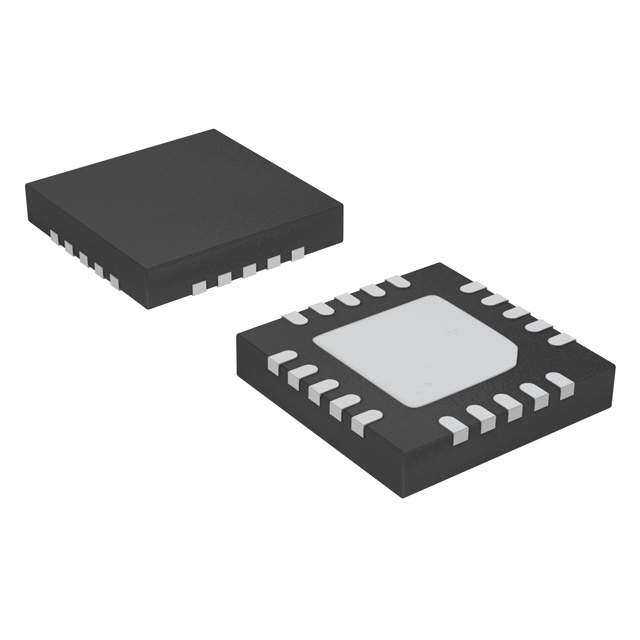
| 供应商器件封装 | 14-VSON (4x3) |
| 其它名称 | 296-27259-2 |
| 包装 | 带卷 (TR) |
| 同步整流器 | 是 |
| 安装类型 | 表面贴装 |
| 封装/外壳 | 14-VFDFN 裸露焊盘 |
| 工作温度 | -40°C ~ 85°C |
| 标准包装 | 3,000 |
| 电压-输入 | 1.8 V ~ 5.5 V |
| 电压-输出 | 3.3V |
| 电流-输出 | 3A |
| 类型 | 降压(降压),升压(升压) |
| 设计资源 | http://www.digikey.com/product-highlights/cn/zh/texas-instruments-webench-design-center/3176 |
| 输出数 | 1 |
| 输出类型 | 固定 |
| 频率-开关 | 2.4MHz |


- 商务部:美国ITC正式对集成电路等产品启动337调查
- 曝三星4nm工艺存在良率问题 高通将骁龙8 Gen1或转产台积电
- 太阳诱电将投资9.5亿元在常州建新厂生产MLCC 预计2023年完工
- 英特尔发布欧洲新工厂建设计划 深化IDM 2.0 战略
- 台积电先进制程称霸业界 有大客户加持明年业绩稳了
- 达到5530亿美元!SIA预计今年全球半导体销售额将创下新高
- 英特尔拟将自动驾驶子公司Mobileye上市 估值或超500亿美元
- 三星加码芯片和SET,合并消费电子和移动部门,撤换高东真等 CEO
- 三星电子宣布重大人事变动 还合并消费电子和移动部门
- 海关总署:前11个月进口集成电路产品价值2.52万亿元 增长14.8%


PDF Datasheet 数据手册内容提取
Product Order Technical Tools & Support & Folder Now Documents Software Community TPS63020,TPS63021 SLVS916G–JULY2010–REVISEDMARCH2019 TPS6302x high efficiency single inductor buck-boost converter with 4-A switches 1 Features 3 Description • InputVoltageRange:1.8Vto5.5V The TPS6302x devices provide a power supply 1 solution for products powered by either a two-cell or • AdjustableOutputVoltage:1.2Vto5.5V three-cell alkaline, NiCd or NiMH battery, a one-cell • OutputCurrentforVIN >2.5V,VOUT=3.3V:2A Li-ion or Li-polymer battery, supercapacitors or other • HighEfficiencyOverTheEntireLoadRange supply rails. Output currents up to 3 A are supported. When using batteries, they can be discharged down – OperatingQuiescentCurrent:25 µA to below 2 V. The buck-boost converter is based on a – PowerSaveModewithModeSelection fixed frequency, pulse width modulation (PWM) • AverageCurrentModeBuck-BoostArchitecture controller using synchronous rectification to obtain maximum efficiency. At low load currents, the – AutomaticTransitionBetweenModes converter enters power save mode to maintain high – FixedFrequencyOperationat2.4MHz efficiency over a wide load current range. The power – SynchronizationPossible save mode can be disabled, forcing the converter to • PowerGoodOutput operate at a fixed switching frequency. The maximum average current in the switches is limited to a typical • SafetyandRobustOperationFeatures value of 4 A. The output voltage is programmable – Overtemperature,OvervoltageProtection using an external resistor divider, or is fixed internally – LoadDisconnectDuringShutdown on the chip. The converter can be disabled to minimize battery drain. During shutdown, the load is • CreateaCustomDesignUsingthe disconnectedfromthebattery. – TPS63020withWEBENCHPowerDesigner The TPS6302x devices operate over a free air – TPS63021withWEBENCHPowerDesigner temperature range of –40 °C to 85 °C. The devices are packaged in a 14-pin VSON package measuring 2 Applications 3mm×4mm(DSJ). • Pre-regulationinBattery-poweredDevices(EPOS DeviceInformation(1) (HandheldTerminal,BarCodeScanner),E- Cigarette,SingleBoardComputer,IPNetwork PARTNUMBER OUTPUTVOLTAGE PACKAGE Camera,VideoDoorbell,Radios) TPS63020 Adjustable VSON(14) • VoltageStabilizer(Wiredorwireless TPS63021 3.3V Communication,PLC,LaserSupply) (1) For all available packages, see the orderable addendum at • BackupSupercapacitorSupply(E-Meter, theendofthedatasheet. EnterpriseSSD) SPACE space SimplifiedSchematic EfficiencyvsOutputCurrent L1 1.5 µH 100 90 L1 L2 VIN VOUT 80 1.8 V to 5.5 V 3.3 V VIN VOUT 70 TPS63020 R1 %) 60 C1 1 0(cid:159)(cid:3) C2 y ( 2×10 µF VINA FB R1820 N(cid:159)(cid:3) 3×22 µF R1 30(cid:159)(cid:3) Efficienc 4500 EN 30 PS/SYNC Power 20 VIN = 1.8 V, VOUT = 2.5 V Good VIN = 3.6 V, VOUT = 2.5 V C3 PG 10 VIN = 2.4 V, VOUT = 4.5 V 100 nF Power-save mode enabled VIN = 3.6 V, VOUT = 4.5 V GND PGND 0 100P 1m 10m 100m 1 Output Current (A) D001 1 An IMPORTANT NOTICE at the end of this data sheet addresses availability, warranty, changes, use in safety-critical applications, intellectualpropertymattersandotherimportantdisclaimers.PRODUCTIONDATA.
TPS63020,TPS63021 SLVS916G–JULY2010–REVISEDMARCH2019 www.ti.com Table of Contents 1 Features.................................................................. 1 8.2 TypicalApplication..................................................13 2 Applications........................................................... 1 8.3 SystemExamples...................................................20 3 Description............................................................. 1 9 PowerSupplyRecommendations...................... 22 4 RevisionHistory..................................................... 2 10 Layout................................................................... 22 5 PinConfigurationandFunctions......................... 4 10.1 LayoutGuidelines.................................................22 10.2 LayoutExample....................................................22 6 Specifications......................................................... 5 10.3 ThermalConsiderations........................................23 6.1 AbsoluteMaximumRatings......................................5 11 DeviceandDocumentationSupport................. 24 6.2 ESDRatings..............................................................5 6.3 RecommendedOperatingConditions.......................5 11.1 CustomDesignwithWEBENCHTools.................24 6.4 ThermalInformation..................................................5 11.2 ReceivingNotificationofDocumentationUpdates24 6.5 ElectricalCharacteristics...........................................6 11.3 DeviceSupport......................................................24 6.6 TypicalCharacteristics..............................................7 11.4 DocumentationSupport........................................24 11.5 RelatedLinks........................................................24 7 DetailedDescription.............................................. 8 11.6 CommunityResources..........................................24 7.1 Overview...................................................................8 11.7 Trademarks...........................................................25 7.2 FunctionalBlockDiagram.........................................8 11.8 ElectrostaticDischargeCaution............................25 7.3 FeatureDescription...................................................9 11.9 Glossary................................................................25 7.4 DeviceFunctionalModes........................................10 12 Mechanical,Packaging,andOrderable 8 ApplicationandImplementation........................ 13 Information........................................................... 25 8.1 ApplicationInformation............................................13 4 Revision History ChangesfromRevisionF(March2019)toRevisionG Page • ChangedtheSimplifiedSchematic,removedtheconnectionfromVINAtoVIN .................................................................. 1 • ChangedFigure7,removedtheconnectionfromVINAtoVIN .......................................................................................... 13 • ChangedFigure28,removedtheconnectionfromVINAtoVIN ........................................................................................ 20 ChangesfromRevisionE(May2017)toRevisionF Page • UpdatedFeaturesandApplicationsonthe1stpage............................................................................................................. 1 • ChangedtheBodySizecolumnTo:OutputVoltageintheDeviceInformationtable........................................................... 1 • ChangedthePinConfigurationimage .................................................................................................................................. 4 • ChangedChapterorderinApplicationInformation............................................................................................................. 13 • Updatedoutputcapacitorselectionsection......................................................................................................................... 15 • AddedTableofTypicalCharacteristicsCurves. ................................................................................................................. 16 • ChangedFigure24andFigure25....................................................................................................................................... 18 • AddedFigure26andFigure27........................................................................................................................................... 19 • ChangedFigure28 .............................................................................................................................................................. 20 • AddedsystemexamplesSupercapacitorBackupPowerSupplyWithActiveCellBalancingandLow-PowerTECDriver 21 ChangesfromRevisionD(October2015)toRevisionE Page • AddedVoltageAC-spectoAbsoluteMaximumRatingstableforL1,L2. ............................................................................. 5 ChangesfromRevisionC(February2013)toRevisionD Page • AddedHandlingRatingtable,FeatureDescriptionsection,DeviceFunctionalModes,Applicationand Implementationsection,PowerSupplyRecommendationssection,Layoutsection,DeviceandDocumentation Supportsection,andMechanical,Packaging,andOrderableInformationsection................................................................ 1 2 SubmitDocumentationFeedback Copyright©2010–2019,TexasInstrumentsIncorporated ProductFolderLinks:TPS63020 TPS63021
TPS63020,TPS63021 www.ti.com SLVS916G–JULY2010–REVISEDMARCH2019 ChangesfromRevisionB(August2012)toRevisionC Page • ChangedFigure7schematictoshowcorrectcomponentvalues....................................................................................... 13 • ChangedFigure28schematictoshowcorrectcomponentvalues..................................................................................... 20 ChangesfromRevisionA(December2011)toRevisionB Page • ChangedtheDutycycleinstepdownconversionvalues,addedMIN=20%,deletedTYP=30%andMAX=40%..........6 ChangesfromOriginal(April2010)toRevisionA Page • UpdatedFigure31-PCBLayoutSuggestion...................................................................................................................... 22 Copyright©2010–2019,TexasInstrumentsIncorporated SubmitDocumentationFeedback 3 ProductFolderLinks:TPS63020 TPS63021
TPS63020,TPS63021 SLVS916G–JULY2010–REVISEDMARCH2019 www.ti.com 5 Pin Configuration and Functions DSJPackage 14-PinVSONWithExposedThermalPad TopView D D D D N N N N G G G G P P P P VINA 1 14 PG GND 2 13 PS/SYNC FB 3 12 EN Thermal Pad VOUT 4 11 VIN VOUT 5 10 VIN L2 6 9 L1 L2 7 8 L1 Not to scaleD D D D N N N N G G G G P P P P PinFunctions PIN I/O DESCRIPTION NAME NO. EN 12 I Enableinput(1enabled,0disabled),mustnotbeleftopen FB 3 I Voltagefeedbackofadjustableversions,mustbeconnectedtoVOUTonfixedoutputvoltage versions GND 2 – Control/logicground L1 8,9 I Connectionforinductor L2 6,7 I Connectionforinductor PG 14 O Outputpowergood(1good,0failure;opendrain),canbeleftopen PGND – Powerground PS/SYNC 13 I Enable/disablepowersavemode(1disabled,0enabled,clocksignalforsynchronization),must notbeleftopen VIN 10,11 I Supplyvoltageforpowerstage VINA 1 I Supplyvoltageforcontrolstage VOUT 4,5 O Buck-boostconverteroutput Exposed – TheexposedthermalpadisconnectedtoPGND. ThermalPad 4 SubmitDocumentationFeedback Copyright©2010–2019,TexasInstrumentsIncorporated ProductFolderLinks:TPS63020 TPS63021
TPS63020,TPS63021 www.ti.com SLVS916G–JULY2010–REVISEDMARCH2019 6 Specifications 6.1 Absolute Maximum Ratings overoperatingfree-airtemperaturerange(unlessotherwisenoted)(1) MIN MAX UNIT VIN,VINA,VOUT,PS/SYNC,EN,FB,PG –0.3 7 V Voltage(2) L1,L2(DC) –0.3 7 V L1,L2(AC,lessthan10ns)(3) –3 10 V Operatingjunctiontemperature,T –40 150 °C J Storagetemperature,T –65 150 °C stg (1) Stressesbeyondthoselistedunderabsolutemaximumratingsmaycausepermanentdamagetothedevice.Thesearestressratings only,andfunctionaloperationofthedeviceattheseoranyotherconditionsbeyondthoseindicatedunderrecommendedoperating conditionsisnotimplied.Exposuretoabsolute-maximum-ratedconditionsforextendedperiodsmyaffectdevicereliability. (2) Allvoltagesarewithrespecttonetworkgroundterminal. (3) Normalswitchingoperation 6.2 ESD Ratings VALUE UNIT Humanbodymodel(HBM),perANSI/ESDA/JEDECJS-001,allpins(1) ±3000 V(ESD) Electrostaticdischarge Chargeddevicemodel(CDM),perJEDECspecificationJESD22-C101, ±1500 V allpins(2) (1) JEDECdocumentJEP155statesthat500-VHBMallowssafemanufacturingwithastandardESDcontrolprocess. (2) JEDECdocumentJEP157statesthat250-VCDMallowssafemanufacturingwithastandardESDcontrolprocess. 6.3 Recommended Operating Conditions MIN NOM MAX UNIT SupplyvoltageatVIN,VINA 1.8 5.5 V Operatingfreeairtemperature,T –40 85 °C A Operatingjunctiontemperature,T –40 125 °C J 6.4 Thermal Information TPS6302x THERMALMETRIC(1) DSJ(VSON) UNIT 14PINS R Junction-to-ambientthermalresistance 41.8 °C/W θJA R Junction-to-case(top)thermalresistance 47 °C/W θJC(top) R Junction-to-boardthermalresistance 17 °C/W θJB ψ Junction-to-topcharacterizationparameter 0.9 °C/W JT ψ Junction-to-boardcharacterizationparameter 16.8 °C/W JB R Junction-to-case(bottom)thermalresistance 3.6 °C/W θJC(bot) (1) Formoreinformationabouttraditionalandnewthermalmetrics,seetheSemiconductorandICPackageThermalMetricsapplication report. Copyright©2010–2019,TexasInstrumentsIncorporated SubmitDocumentationFeedback 5 ProductFolderLinks:TPS63020 TPS63021
TPS63020,TPS63021 SLVS916G–JULY2010–REVISEDMARCH2019 www.ti.com 6.5 Electrical Characteristics overrecommendedfree-airtemperaturerangeandoverrecommendedinputvoltagerange(typicalatanambienttemperature rangeof25°C)(unlessotherwisenoted) PARAMETER TESTCONDITIONS MIN TYP MAX UNIT DC/DCSTAGE Inputvoltage 1.8 5.5 V V Minimuminputvoltageforstartup 0°C≤T ≤85°C 1.5 1.8 1.9 V IN A Minimuminputvoltageforstartup 1.5 1.8 2.0 V V TPS63020outputvoltage 1.2 5.5 V OUT Dutycycleinstepdownconversion 20% V TPS63020feedbackvoltage 495 500 505 mV FB PS/SYNC=V IN TPS63021outputvoltage 3.267 3.3 3.333 V V TPS63020feedbackvoltageregulation PS/SYNC=GNDreferencedto500mV 0.6% 5% FB TPS63021outputvoltageregulation PS/SYNC=GNDreferencedto3.3V 0.6% 5% Maximumlineregulation 0.5% Maximumloadregulation 0.5% f Oscillatorfrequency 2200 2400 2600 kHz Frequencyrangeforsynchronization 2200 2400 2600 kHz I Averageswitchcurrentlimit V =V =3.6V,T =25°C 3500 4000 4500 mA SW IN INA A Highsideswitchonresistance V =V =3.6V 50 mΩ IN INA Lowsideswitchonresistance V =V =3.6V 50 mΩ IN INA Quiescent VINandVINA I =0mA,V =V =V =3.6V, 25 50 μA I OUT EN IN INA q current VOUT VOUT=3.3V 5 10 μA TPS63021FBinputimpedance V =HIGH 1 MΩ EN I Shutdowncurrent V =0V,V =V =3.6V 0.1 1 μA S EN IN INA CONTROLSTAGE Undervoltagelockoutthreshold V voltagedecreasing 1.4 1.5 1.6 V INA UVLO Undervoltagelockouthysteresis 200 mV V EN,PS/SYNCinputlowvoltage 0.4 V IL V EN,PS/SYNCinputhighvoltage 1.2 V IH EN,PS/SYNCinputcurrent ClampedtoGNDorVINA 0.01 0.1 μA PGoutputlowvoltage V =3.3V,I =10μA 0.04 0.4 V OUT PGL PGoutputleakagecurrent 0.01 0.1 μA Outputovervoltageprotection 5.5 7 V Overtemperatureprotection 140 °C Overtemperaturehysteresis 20 °C 6 SubmitDocumentationFeedback Copyright©2010–2019,TexasInstrumentsIncorporated ProductFolderLinks:TPS63020 TPS63021
TPS63020,TPS63021 www.ti.com SLVS916G–JULY2010–REVISEDMARCH2019 6.6 Typical Characteristics 4 4 TPS63020 TPS63021 3.5 3.5 3 3 A) A) nt ( nt ( urre 2.5 urre 2.5 C C put 2 put 2 ut ut O O m m u 1.5 u 1.5 m m xi xi a a M M 1 1 0.5 0.5 VOUT = 2.5V VOUT = 4.5V VOUT = 3.3V 0 0 1.8 2.2 2.6 3 3.4 3.8 4.2 4.6 5 5.4 1.8 2.2 2.6 3 3.4 3.8 4.2 4.6 5 5.4 Input Voltage (V) Input Voltage (V) Figure1.MaximumOutputCurrentvsInputVoltage, Figure2.MaximumOutputCurrentvsInputVoltage, TPS63020,V =2.5V/4.5V TPS63021,V =3.3V OUT OUT Copyright©2010–2019,TexasInstrumentsIncorporated SubmitDocumentationFeedback 7 ProductFolderLinks:TPS63020 TPS63021
TPS63020,TPS63021 SLVS916G–JULY2010–REVISEDMARCH2019 www.ti.com 7 Detailed Description 7.1 Overview The control circuit of the device is based on an average current mode topology. The controller also uses input and output voltage feed forward. Changes of input and output voltage are monitored and immediately can change the duty cycle in the modulator to achieve a fast response to those errors. The voltage error amplifier gets its feedback input from the FB pin. At adjustable output voltages, a resistive voltage divider must be connected to that pin. At fixed output voltages, FB must be connected to the output voltage to directly sense the voltage. Fixed output voltage versions use a trimmed internal resistive divider. The feedback voltage will be comparedwiththeinternalreferencevoltagetogenerateastableandaccurateoutputvoltage. The device uses 4 internal N-channel MOSFETs to maintain synchronous power conversion at all possible operating conditions. This enables the device to keep high efficiency over a wide input voltage and output power range. To avoid ground shift problems due to the high currents in the switches, two separate ground pins GND and PGND are used. The reference for all control functions is the GND pin. The power switches are connected to PGND. Both grounds must be connected on the PCB at only one point, ideally close to the GND pin. Due to the 4-switch topology, the load is always disconnected from the input during shutdown of the converter. To protect thedevicefromoverheatinganinternaltemperaturesensorisimplemented. 7.2 Functional Block Diagram L1 L2 VIN VOUT Current Sensor VINA PGND PGND VIN Gate VOUT Control _ VINA Modulator + FB + _ PG Oscillator + VREF - Device PS/SYNC Control EN Temperature Control PGND GND PGND Copyright © 2017,Texas Instruments Incorporated Figure3. FunctionalBlockDiagram(TPS63020) 8 SubmitDocumentationFeedback Copyright©2010–2019,TexasInstrumentsIncorporated ProductFolderLinks:TPS63020 TPS63021
TPS63020,TPS63021 www.ti.com SLVS916G–JULY2010–REVISEDMARCH2019 Functional Block Diagram (continued) L1 L2 VIN VOUT Current Sensor VINA PGND PGND VIN Gate VOUT FB Control _ VINA Modulator + + _ PG Oscillator + - Device VREF PS/SYNC Control EN Temperature Control PGND GND PGND Copyright © 2017,Texas Instruments Incorporated Figure4. FunctionalBlockDiagram(TPS63021) 7.3 Feature Description 7.3.1 DynamicVoltagePositioning As detailed in Figure 6, the output voltage is typically 3% above the nominal output voltage at light load currents, as the device is in power save mode. This gives additional headroom for the voltage drop during a load transient from light load to full load. This allows the converter to operate with a small output capacitor and still have a low absolutevoltagedropduringheavyloadtransientchanges. 7.3.2 DynamicCurrentLimit To protect the device and the application, the average inductor current is limited internally on the IC. At nominal operating conditions, this current limit is constant. The current limit value can be found in the electrical characteristicstable.IfthesupplyvoltageatVINdropsbelow2.3V,thecurrentlimitisreduced.Thiscanhappen when the input power source becomes weak. Increasing output impedance, when the batteries are almost discharged, or an additional heavy pulse load is connected to the battery can cause the VIN voltage to drop. The dynamic current limit has its lowest value when reaching the minimum recommended supply voltage at VIN. At this voltage, the device is forced into burst mode operation trying to stay active as long as possible even with a weakinputpowersource. If the die temperature increases above the recommended maximum temperature, the dynamic current limit becomes active. Similar to the behavior when the input voltage at VIN drops, the current limit is reduced with temperatureincreasing. Copyright©2010–2019,TexasInstrumentsIncorporated SubmitDocumentationFeedback 9 ProductFolderLinks:TPS63020 TPS63021
TPS63020,TPS63021 SLVS916G–JULY2010–REVISEDMARCH2019 www.ti.com Feature Description (continued) 7.3.3 DeviceEnable The device is put into operation when EN is set high. It is put into a shutdown mode when EN is set to GND. In shutdown mode, the regulator stops switching, all internal control circuitry is switched off, and the load is disconnected from the input. This means that the output voltage can drop below the input voltage during shutdown. During start-up of the converter, the duty cycle and the peak current are limited in order to avoid high peakcurrentsflowingfromtheinput. 7.3.4 PowerGood The device has a built in power good function to indicate whether the output voltage is regulated properly. As soon as the average inductor current limit is reached the power good output gets low impedance. The output is open drain and can be left open if not needed. By connecting a pull up resistor to the supply voltage of the externallyconnectedlogic,itispossibletoadjustthevoltagelevelwithintheabsolutemaximumratings. Because it is monitoring the status of the current control loop, the power good output provides the earliest indication possible for an output voltage break down and leaves the connected application a maximum time to safelyreact. 7.3.5 OvervoltageProtection If, for any reason, the output voltage is not fed back properly to the input of the voltage amplifier, control of the output voltage will not work anymore. Therefore overvoltage protection is implemented to avoid the output voltage exceeding critical values for the device and possibly for the system it is supplying. The implemented overvoltage protection circuit monitors the output voltage internally as well. In case it reaches the overvoltage thresholdthevoltageamplifierregulatestheoutputvoltagetothisvalue. 7.3.6 UndervoltageLockout An undervoltage lockout function prevents device start-up if the supply voltage on VINA is lower than approximately its threshold (see Electrical Characteristics). When in operation, the device automatically enters the shutdown mode if the voltage at VINA drops below the undervoltage lockout threshold. The device automaticallyrestartsiftheinputvoltagerecoverstotheminimumoperatinginputvoltage. 7.3.7 OvertemperatureProtection The device has a built-in temperature sensor which monitors the internal IC temperature. If the temperature exceeds the programmed threshold (see Electrical Characteristics) the device stops operating. As soon as the IC temperature has decreased below the programmed threshold, it starts operating again. There is a built-in hysteresistoavoidunstableoperationatICtemperaturesattheovertemperaturethreshold. 7.4 Device Functional Modes 7.4.1 SoftstartandShortCircuitProtection After being enabled, the device starts operating. The average current limit ramps up from an initial 400 mA following the output voltage increasing. At an output voltage of about 1.2 V, the current limit is at its nominal value. If the output voltage does not increase, the current limit will not increase. There is no timer implemented. Thus, the output voltage overshoot at startup, as well as the inrush current, is kept at a minimum. The device ramps up the output voltage in a controlled manner even if a large capacitor is connected at the output. When the output voltage does not increase above 1.2 V, the device assumes a short circuit at the output, and keeps thecurrentlimitlowtoprotectitselfandtheapplication.Atashortontheoutputduringoperation,thecurrentlimit alsoisdecreasedaccordingly. 7.4.2 Buck-BoostOperation To regulate the output voltage at all possible input voltage conditions, the device automatically switches from step down operation to boost operation and back as required by the configuration. It always uses one active switch, one rectifying switch, one switch permanently on, and one switch permanently off. Therefore, it operates as a step down converter (buck) when the input voltage is higher than the output voltage, and as a boost converter when the input voltage is lower than the output voltage. There is no mode of operation in which all 4 10 SubmitDocumentationFeedback Copyright©2010–2019,TexasInstrumentsIncorporated ProductFolderLinks:TPS63020 TPS63021
TPS63020,TPS63021 www.ti.com SLVS916G–JULY2010–REVISEDMARCH2019 Device Functional Modes (continued) switches are permanently switching. Controlling the switches this way allows the converter to maintain high efficiency at the most important point of operation, when input voltage is close to the output voltage. The RMS currentthroughtheswitchesandtheinductoriskeptataminimum,tominimizeswitchingandconductionlosses. For the remaining 2 switches, one is kept permanently on and the other is kept permanently off, thus causing no switchinglosses. 7.4.3 ControlLoop The controller circuit of the device is based on an average current mode topology. The average inductor current is regulated by a fast current regulator loop which is controlled by a voltage control loop. Figure 5 shows the controlloop. The non inverting input of the transconductance amplifier, gmv, is assumed to be constant. The output of gmv defines the average inductor current. The inductor current is reconstructed by measuring the current through the high side buck MOSFET. This current corresponds exactly to the inductor current in boost mode. In buck mode the current is measured during the on time of the same MOSFET. During the off time, the current is reconstructed internally starting from the peak value at the end of the on time cycle. The average current and the feedback from the error amplifier gmv forms the correction signal gmc. This correction signal is compared to the buck and the boost sawtooth ramp giving the PWM signal. Depending on which of the two ramps the gmc output crosses either the Buck or the Boost stage is initiated. When the input voltage is close to the output voltage, one buck cycle is always followed by a boost cycle. In this condition, no more than three cycles in a row of the same mode are allowed. This control method in the buck-boost region ensures a robust control and the highest efficiency. The Buck-Boost Overlap ControlTM makes sure that the classical buck-boost function, which would cause two switches to be on every half a cycle, is avoided. Thanks to this block whenever all switches becomes active during one clock cycle, the two ramps are shifted away from each other, on the other hand when there is no switching activities because there is a gap between the ramps, the ramps are moved closer together. As a result the number of classical buck-boost cycles or no switching is reduced to a minimum and high efficiency values hasbeenachieved. TM Figure5. AverageCurrentModeControl Copyright©2010–2019,TexasInstrumentsIncorporated SubmitDocumentationFeedback 11 ProductFolderLinks:TPS63020 TPS63021
TPS63020,TPS63021 SLVS916G–JULY2010–REVISEDMARCH2019 www.ti.com Device Functional Modes (continued) 7.4.4 PowerSaveModeandSynchronization The PS/SYNC pin can be used to select different operation modes. Power save mode is used to improve efficiency at light load. To enable power save mode, PS/SYNC must be set low. If PS/SYNC is set low then power save mode is entered when the average inductor current gets lower than about 100 mA. At this point the converter operates with reduced switching frequency and with a minimum quiescent current to maintain high efficiency.SeeFigure6fordetailedoperationofthepowersavemode. During the power save mode, the output voltage is monitored with a comparator by the threshold comp low and comp high. When the device enters power save mode, the converter stops operating and the output voltage drops. The slope of the output voltage depends on the load and the value of output capacitance. As the output voltage falls below the comp low threshold set to 2.5% typical above V , the device ramps up the output OUT voltage again, by starting operation using a programmed average inductor current higher than required by the current load condition. Operation can last one or several pulses. The converter continues these pulses until the comp high threshold, set to typically 3.5% above V nominal, is reached and the average inductance current OUT getslowerthanabout100mA.Whentheloadincreasesabovetheminimumforcedinductorcurrentofabout100 mA,thedevicewillautomaticallyswitchtopulsewidthmodulation(PWM)mode. The power save mode can be disabled by programming high at the PS/SYNC. Connecting a clock signal at PS/SYNCforcesthedevicetosynchronizetotheconnectedclockfrequency. Synchronization is done by a phase-locked loop (PLL), so synchronizing to lower and higher frequencies compared to the internal clock works without any issues. The PLL can also tolerate missing clock pulses without theconvertermalfunctioning.ThePS/SYNCinputsupportsstandardlogicthresholds. Heavy Load transient step Power save mode at light load current 3.5% Comparator High 3% 2.5% Comparator low Vo PWM mode Absolute Voltage drop with positioning Figure6. PowerSaveModeThresholdsandDynamicVoltagePositioning 12 SubmitDocumentationFeedback Copyright©2010–2019,TexasInstrumentsIncorporated ProductFolderLinks:TPS63020 TPS63021
TPS63020,TPS63021 www.ti.com SLVS916G–JULY2010–REVISEDMARCH2019 8 Application and Implementation NOTE Information in the following applications sections is not part of the TI component specification, and TI does not warrant its accuracy or completeness. TI’s customers are responsible for determining suitability of components for their purposes. Customers should validateandtesttheirdesignimplementationtoconfirmsystemfunctionality. 8.1 Application Information The TPS6302x are high efficiency, low quiescent current, non-inverting buck-boost converters suitable for applications that need a regulated output voltage from an input supply that can be higher, lower or equal to the output voltage. Output currents can go as high as 2 A in boost mode and as high as 4 A in buck mode. The averagecurrentintheswitchesislimitedtoatypicalvalueof4A. 8.2 Typical Application L1 1.5 µH L1 L2 V V IN OUT 2.5 V to 5.5 V 3.3 V at 1.5 A VIN VOUT TPS63020 R1 C1 1 M(cid:159)(cid:3) C2 2×10 µF 3×22 µF FB R3 R2 1 M(cid:159)(cid:3) VINA 180 k(cid:159)(cid:3) EN PS/SYNC Power Good PG C3 100 nF GND PGND Figure7. ApplicationCircuit 8.2.1 DesignRequirements The design guideline provides a component selection to operate the device within the recommended operating conditions,seeTable1forpossibleinductorandcapacitorcombinations. ForthefixedoutputvoltageoptionthefeedbackpinneedstobeconnectedtotheVOUTpin. Table1.MatrixofOutputCapacitorandInductorCombinations NominalInductor NominalOutputCapacitorValue[µF](2) Value[µH](1) 2×22 3×22 4×22 ≥100 1.0 + + + 1.5 + +(3) + + 2.2 + + (1) Inductortoleranceandcurrentderatingisanticipated.Theeffectiveinductancecanvaryby20%and–30%. (2) CapacitancetoleranceandDCbiasvoltagederatingisanticipated.Theeffectivecapacitancecanvaryby20%and–50%. (3) Typicalapplication.Othercheckmarksindicatepossiblefiltercombinations. Copyright©2010–2019,TexasInstrumentsIncorporated SubmitDocumentationFeedback 13 ProductFolderLinks:TPS63020 TPS63021
TPS63020,TPS63021 SLVS916G–JULY2010–REVISEDMARCH2019 www.ti.com 8.2.2 DetailedDesignProcedure The TPS6302x series of buck-boost converter has internal loop compensation. Therefore, the external inductor and output capacitors have to be selected to work with the internal compensation. When selecting the external components, a low limit for the inductor value exists to avoid sub-harmonic oscillation which could be caused by a far too fast ramp up of the inductor current. For the TPS6302x series the inductor value should be kept at or above1µH. In particular either 1 µH or 1.5 µH is recommended working at an output current between 1.5 A and 2 A. If operatingwithalowerloadcurrentitisalsopossibletouse2.2 µH. Selecting a larger output capacitor value is less critical because the corner frequency moves to lower frequencies. 8.2.2.1 CustomDesignwithWEBENCHTools ClickheretocreateacustomdesignusingtheTPS63020devicewiththe WEBENCH® PowerDesigner. 1. StartbyenteringyourV ,V andI requirements. IN OUT OUT 2. Optimize your design for key parameters like efficiency, footprint or cost using the optimizer dial and comparethisdesignwithotherpossiblesolutionsfromTexasInstruments. 3. WEBENCH Power Designer provides you with a customized schematic along with a list of materials with real timepricingandcomponentavailability. 4. Inmostcases,youwillalsobeableto: – Runelectricalsimulationstoseeimportantwaveformsandcircuitperformance, – Runthermalsimulationstounderstandthethermalperformanceofyourboard, – ExportyourcustomizedschematicandlayoutintopopularCADformats, – PrintPDFreportsforthedesign,andshareyourdesignwithcolleagues. 5. GetmoreinformationaboutWEBENCHtoolsatwww.ti.com/webench. 8.2.2.2 InductorSelection The inductor selection is affected by several parameters such as inductor ripple current, output voltage ripple, transitionpointintoPowerSaveMode,andefficiency.SeeTable2 fortypicalinductors. For high efficiencies, the inductor should have a low DC resistance to minimize conduction losses. Especially at high-switching frequencies, the core material has a high impact on efficiency. When using small chip inductors, the efficiency is reduced mainly due to higher inductor core losses. This needs to be considered when selecting the appropriate inductor. The inductor value determines the inductor ripple current. The larger the inductor value, the smaller the inductor ripple current and the lower the conduction losses of the converter. Conversely, larger inductor values cause a slower load transient response. To avoid saturation of the inductor, the peak current for the inductor in steady state operation is calculated using Equation 2. Only the equation which defines the switch current in boost mode is shown, because this provides the highest value of current and represents the critical currentvalueforselectingtherightinductor. V -V OUT IN DutyCycleBoost D= V OUT (1) Iout Vin ´ D I = + PEAK η ´ (1 - D) 2 ´ f ´ L (2) where: • D=DutyCycleinBoostmode • f=Converterswitchingfrequency(typical2.5MHz) • L=Inductorvalue • η=Estimatedconverterefficiency(usethenumberfromtheefficiencycurvesor0.9asanassumption) NOTE Thecalculationmustbedonefortheminimuminputvoltageinboostmode. 14 SubmitDocumentationFeedback Copyright©2010–2019,TexasInstrumentsIncorporated ProductFolderLinks:TPS63020 TPS63021
TPS63020,TPS63021 www.ti.com SLVS916G–JULY2010–REVISEDMARCH2019 Calculating the maximum inductor current using the actual operating conditions gives the minimum saturation current of the inductor needed. It is recommended to choose an inductor with a saturation current 20% higher thanthevaluecalculatedusingEquation2.PossibleinductorsarelistedinTable2. Table2.ListofRecommendedInductors (1) Inductor SaturationCurrent[A] DCR[mΩ] PartNumber Manufacturer Size(LxWxH Value[µH] mm) 1.5 5.1 15 XFL4020-152ME Coilcraft 4x4x2.1 1.5 5.4 24 FDV0530S-H-1R5M muRata 5x5x3 (1) SeeThird-partyProductsDisclaimer 8.2.2.3 OutputCapacitorSelection For the output capacitor, use of small ceramic capacitors placed as close as possible to the VOUT and PGND pins of the IC is recommended. The recommended nominal output capacitors are three times 22 µF. If, for any reason, the application requires the use of large capacitors which can not be placed close to the IC, use a smaller ceramic capacitor in parallel to the large capacitor. The small capacitor should be placed as close as possibletotheVOUTandPGNDpinsoftheIC. There are no additional requirements regarding minimum ESR. There is also no upper limit for the output capacitance value. Larger capacitors will cause lower output voltage ripple as well as lower output voltage drop duringloadtransients. 8.2.2.4 InputCapacitorSelection A 10 µF input capacitor is recommended to improve line transient behavior of the regulator and EMI behavior of the total power supply circuit. An X5R or X7R ceramic capacitor placed as close as possible to the VIN and PGND pins of the IC is recommended. This capacitance can be increased without limit. If the input supply is located more than a few inches from the TPS6302x converter additional bulk capacitance may be required in addition to the ceramic bypass capacitors. An electrolytic or tantalum capacitor with a value of 47 µF is a typical choice. 8.2.2.5 BypassCapacitor Tomakesurethattheinternalcontrolcircuitsaresuppliedwithastablelownoisesupplyvoltage,acapacitorcan be connected between VINA and GND. Using a ceramic capacitor with a value of 0.1 µF is recommended. The valueofthiscapacitorshouldnotbehigherthan0.22µF. 8.2.3 SettingTheOutputVoltage When the adjustable output voltage version TPS63020 is used, the output voltage is set by an external resistor divider. The resistor divider must be connected between VOUT, FB and GND. The feedback voltage is 500 mV nominal.Thelow-sideresistorR2(betweenFBandGND)shouldbekeptintherangeof200kΩ.UseEquation3 tocalculatethehigh-sideresistorR1(betweenVOUTandFB). æV ö R1 = R2× ç OUT -1÷ V è FB ø (3) whereV =500mV. FB Table3.ResistorSelectionForTypicalOutputVoltages V R1 R2 OUT 2.5V 750kΩ 180kΩ 3.3V 1MΩ 180kΩ 3.6V 1.1MΩ 180kΩ 4.5V 1.43MΩ 180kΩ 5V 1.6MΩ 180kΩ Copyright©2010–2019,TexasInstrumentsIncorporated SubmitDocumentationFeedback 15 ProductFolderLinks:TPS63020 TPS63021
TPS63020,TPS63021 SLVS916G–JULY2010–REVISEDMARCH2019 www.ti.com 8.2.4 ApplicationCurves Table4.ComponentsforApplicationCharacteristicCurvesforV =3.3V(1)(2) OUT Reference Description PartNumber Manufacturer U1 HighEfficiencySingleInductorBuck-Boost TPS63020orTPS63021 TexasInstruments ConverterWith4-ASwitches L1 1.5μH,4mmx4mmx2mm XFL4020-152ML Coilcraft C1 2×10μF6.3V,0603,X5Rceramic GRM188R60J106ME84D muRata C2 3×22μF6.3V,0603,X5Rceramic GRM188R60J226MEAOL muRata C3 0.1μF,X5RorX7Rceramic Standard Standard R1 1MΩatTPS63020,0ΩatTPS63021 Standard Standard R2 180kΩatTPS63020,notusedatTPS63021 Standard Standard R3 1MΩ Standard Standard (1) SeeThird-PartyProductsDiscalimer (2) ForotheroutputvoltagesrefertoTable3forresistorvalues. Table5.TypicalCharacteristicsCurves Parameter Conditions Figure Efficiency EfficiencyvsOutputCurrent,TPS63020(Powersavemode V =1.8V,2.4V,3.6V,V =2.5V,4.5V, IN OUT Figure8 enabled) PS/SYNC=Low V =1.8V,2.4V,3.6V,V =2.5V,4.5V, EfficiencyvsOutputCurrent,TPS63020(PWMonly) IN OUT Figure9 PS/SYNC=High EfficiencyvsOutputCurrent,TPS63021(Powersavemode V =2.4V,3.6V,V =3.3V,PS/SYNC= IN OUT Figure10 enabled) Low V =2.4V,3.6V,V =3.3V,PS/SYNC= EfficiencyvsOutputCurrent,TPS63021(PWMonly) IN OUT Figure11 High EfficiencyvsInputVoltage,TPS63020(Powersavemode V =2.5V,Load=10mA,500mA,1A,2A, OUT Figure12 enabled) PS/SYNC=Low EfficiencyvsInputVoltage,TPS63020(Powersavemode V =4.5V,Load=10mA,500mA,1A,2A, OUT Figure13 enabled) PS/SYNC=Low V =2.5V,Load=10mA,500mA,1A,2A, EfficiencyvsInputVoltage,TPS63020(PWMonly) OUT Figure14 PS/SYNC=Low V =2.5V,Load=10mA,500mA,1A,2A, EfficiencyvsInputVoltage,TPS63020(PWMonly) OUT Figure15 PS/SYNC=Low EfficiencyvsInputVoltage,TPS63021(Powersavemode V =3.3V,Load=10mA,500mA,1A,2A, OUT Figure16 enabled) PS/SYNC=Low V =3.3V,Load=10mA,500mA,1A,2A, EfficiencyvsInputVoltage,TPS63021(PWMonly) OUT Figure17 PS/SYNC=Low RegulationAccuracy LoadRegulation,PWMBoostOperation,TPS63020 V =3.6V,V =4.5V,PS/SYNC=High Figure18 IN OUT LoadRegulation,PWMBuckOperation,TPS63020 V =3.6V,V =2.5V,PS/SYNC=High Figure19 IN OUT LoadRegulation,PWMOperation,TPS63021 V =3.6V,V =3.3V,PS/SYNC=High Figure20 IN OUT V =2.4V,V =3.3V,Load=500mAto LoadTransient,TPS63021 IN OUT Figure21 1.5A V =4.2V,V =3.3V,Load=500mAto LoadTransient,TPS63021 IN OUT Figure22 1.5A LineTransient,TPS63021 V =3.0Vto3.7V,V =3.3V,Load=1.5A Figure23 IN OUT Startup Start-upBehaviorfromRisingEnable,TPS63021 V =2.4V,V =3.3V,Load=2.2Ω Figure24 IN OUT Start-upBehaviorfromRisingEnable,TPS63021 V =4.2V,V =3.3V,Load=2.2Ω Figure25 IN OUT Start-upBehaviorfromRisingEnable,TPS63021 V =2.4V,V =3.3V,Load=2.2Ω Figure26 IN OUT Start-upBehaviorfromRisingEnable,TPS63021 V =4.2V,V =3.3V,Load=2.2Ω Figure27 IN OUT 16 SubmitDocumentationFeedback Copyright©2010–2019,TexasInstrumentsIncorporated ProductFolderLinks:TPS63020 TPS63021
TPS63020,TPS63021 www.ti.com SLVS916G–JULY2010–REVISEDMARCH2019 100 100 90 90 80 80 70 70 %) 60 %) 60 ncy ( 50 ncy ( 50 e e Effici 40 Effici 40 30 30 VIN = 1.8V, VOUT = 2.5V VIN = 1.8V, VOUT = 2.5V 20 VIN = 3.6V, VOUT = 2.5V 20 VIN = 3.6V, VOUT = 2.5V VIN = 2.4V, VOUT = 4.5V VIN = 2.4V, VOUT = 4.5V 10 VIN = 3.6V, VOUT = 4.5V 10 VIN = 3.6V, VOUT = 4.5V TPS63020, Power Save Enabled TPS63020, Power Save Disabled 0 0 100µ 1m 10m 100m 1 4 100µ 1m 10m 100m 1 4 Output Current (A) Output Current (A) Figure8.EfficiencyvsOutputCurrent,TPS63020,Power Figure9.EfficiencyvsOutputCurrent,TPS63020,Power SaveEnabled SaveDisabled 100 100 90 90 80 80 70 70 %) 60 %) 60 ncy ( 50 ncy ( 50 e e Effici 40 Effici 40 30 30 20 20 VIN = 2.4V VIN = 2.4V 10 VIN = 3.6V 10 VIN = 3.6V TPS63021, Power Save Enabled TPS63021, Power Save Disabled 0 0 100µ 1m 10m 100m 1 4 100µ 1m 10m 100m 1 4 Output Current (A) Output Current (A) Figure10.EfficiencyvsOutputCurrent,TPS63021,Power Figure11.EfficiencyvsOutputCurrent,TPS63021,Power SaveEnabled SaveDisabled 100 100 90 90 80 80 70 70 %) 60 %) 60 ncy ( 50 ncy ( 50 e e Effici 40 Effici 40 30 30 IOUT = 10mA IOUT = 10mA 20 IOUT = 500mA 20 IOUT = 500mA IOUT = 1A IOUT = 1A 10 IOUT = 2A 10 IOUT = 2A TPS63020, VOUT = 2.5V, Power Save Enabled TPS63020, VOUT = 4.5V, Power Save Enabled 0 0 1.8 2.2 2.6 3 3.4 3.8 4.2 4.6 5 5.4 1.8 2.2 2.6 3 3.4 3.8 4.2 4.6 5 5.4 Input Voltage (V) Input Voltage (V) Figure12.EfficiencyvsInputVoltage,TPS63020,V = Figure13.EfficiencyvsInputVoltage,TPS63020,V = OUT OUT 2.5V,PowerSaveEnabled 4.5V,PowerSaveEnabled Copyright©2010–2019,TexasInstrumentsIncorporated SubmitDocumentationFeedback 17 ProductFolderLinks:TPS63020 TPS63021
TPS63020,TPS63021 SLVS916G–JULY2010–REVISEDMARCH2019 www.ti.com 100 100 90 90 80 80 70 70 %) 60 %) 60 ncy ( 50 ncy ( 50 e e Effici 40 Effici 40 30 30 IOUT = 10mA IOUT = 10mA 20 IOUT = 500mA 20 IOUT = 500mA IOUT = 1A IOUT = 1A 10 IOUT = 2A 10 IOUT = 2A TPS63020, VOUT = 2.5V, Power Save Disabled TPS63020, VOUT = 4.5V, Power Save Disabled 0 0 1.8 2.2 2.6 3 3.4 3.8 4.2 4.6 5 5.4 1.8 2.2 2.6 3 3.4 3.8 4.2 4.6 5 5.4 Input Voltage (V) Input Voltage (V) Figure14.EfficiencyvsInputVoltage,TPS63020,V = Figure15.EfficiencyvsInputVoltage,TPS63020,V = OUT OUT 2.5V,PowerSaveDisabled 4.5V,PowerSaveDisabled 100 100 90 90 80 80 70 70 %) 60 %) 60 ncy ( 50 ncy ( 50 e e Effici 40 Effici 40 30 30 IOUT = 10mA IOUT = 10mA 20 IOUT = 500mA 20 IOUT = 500mA IOUT = 1A IOUT = 1A 10 IOUT = 2A 10 IOUT = 2A TPS63021, Power Save Enabled TPS63021, Power Save Disabled 0 0 1.8 2.2 2.6 3 3.4 3.8 4.2 4.6 5 5.4 1.8 2.2 2.6 3 3.4 3.8 4.2 4.6 5 5.4 Input Voltage (V) Input Voltage (V) Figure16.EfficiencyvsInputVoltage,TPS63021,Power Figure17.EfficiencyvsInputVoltage,TPS63021,Power SaveEnabled SaveDisabled 4.6 2.6 VIN = 3.6V VIN = 3.6V 4.55 2.55 V) V) e ( e ( g g a a olt 4.5 olt 2.5 V V ut ut p p ut ut O O 4.45 2.45 TPS63020, Power Save Disabled TPS63020, Power Save Disabled 4.4 2.4 100µ 1m 10m 100m 1 5 100µ 1m 10m 100m 1 5 Output Current (A) Output Current (A) Figure18.OutputVoltagevsOutputCurrent,TPS63020, Figure19.OutputVoltagevsOutputCurrent,TPS63020, PowerSaveDisabled PowerSaveEnabled 18 SubmitDocumentationFeedback Copyright©2010–2019,TexasInstrumentsIncorporated ProductFolderLinks:TPS63020 TPS63021
TPS63020,TPS63021 www.ti.com SLVS916G–JULY2010–REVISEDMARCH2019 3.4 VIN = 3.6V Output Voltage 3.35 50 mV/div, AC V) e ( g a olt 3.3 V ut p ut O Output Current 500 mA/div, DC 3.25 TPS63021, Power Save Disabled TPS63021 VIN= 2.4 V, IOUT= 500 mAto 1500 mA 3.2 100µ 1m 10m 100m 1 5 Time 2 ms/div Output Current (A) Figure20.OutputVoltagevsOutputCurrent,TPS63021, PowerSaveDisabled Figure21.LoadTransientResponse,TPS63021 Output Voltage 50 mV/div, AC Output Voltage 50 mV/div, AC Output Current 500 mA/div, DC Input Voltage 500 mV/div, AC TPS63021 VIN= 4.2 V, IOUT= 500 mAto 1500 mA TPS63021 VIN= 3.0 V to 3.7 V, IOUT= 1500 mA Time 2 ms/div Time 2 ms/div Figure22.LoadTransientResponse,TPS63021 Figure23.LineTransientResponse,TPS63021 Enable Enable Output Voltage 2V/div, DC Output Voltage 2V/div, DC 1 V/div, DC 1 V/div, DC Inductor Current Inductor Current 1A/div, DC 1A/div, DC Voltage at L1 Voltage at L2 5 V/div, DC 5 V/div, DC TPS63020 VIN=2.4V, VOUT= 3.3 V, RL=2.2W TPS63020 VIN= 4 .2 V, VOUT= 3.3 V, RL=2.2W Time 100ms/div Time 100ms/div Figure25.Start-upBehaviorfromRisingEnable, Figure24.Start-upBehaviorfromRisingEnable, TPS63020 TPS63020 Copyright©2010–2019,TexasInstrumentsIncorporated SubmitDocumentationFeedback 19 ProductFolderLinks:TPS63020 TPS63021
TPS63020,TPS63021 SLVS916G–JULY2010–REVISEDMARCH2019 www.ti.com Enable Enable Output Voltage 2V/div, DC Output Voltage 2V/div, DC 1 V/div, DC 1 V/div, DC Inductor Current Inductor Current 1A/div, DC 1A/div, DC Voltage at L2 Voltage at L2 2 V/div, DC 2 V/div, DC TPS63020 VIN= 2.4 V, VOUT= 3.3 V, RL=2.2W TPS63020 VIN= 4 .2 V, VOUT= 3.3 V, RL=2.2W Time 100ms/div Time 400ms/div Figure27.Start-upBehaviorfromRisingEnable, Figure26.Start-upBehaviorfromRisingEnable, TPS63020 TPS63020 8.3 System Examples 8.3.1 ImprovedTransientResponsefor2ALoadCurrent CapacitorC4andresistorR4areaddedforimprovedloadtransientperformance. L1 1 µH L1 L2 V V IN OUT 2.5 V to 5.5 V 3.3 V at 2 A VIN VOUT R3 TPS63020 R1 68 k(cid:159)(cid:3) C1 1 M(cid:159)(cid:3) C2 2×10 µF 4×22 µF C4 R3 FB 4.7 pF 1 M(cid:159)(cid:3) VINA R2 EN 180 k(cid:159)(cid:3) PS/SYNC Power Good C3 PG 100 nF GND PGND Figure28. ApplicationCircuitfor2ALoadCurrent 20 SubmitDocumentationFeedback Copyright©2010–2019,TexasInstrumentsIncorporated ProductFolderLinks:TPS63020 TPS63021
TPS63020,TPS63021 www.ti.com SLVS916G–JULY2010–REVISEDMARCH2019 System Examples (continued) 8.3.2 SupercapacitorBackupPowerSupplyWithActiveCellBalancing The TPS63020 can be used to charge backup capacitors to a user defined voltage level while the main power supply is supplying a system, and discharge these capacitors into the system when the main power supply is interrupted. With this design, the system voltage during backup operation keeps constant independent of the voltagereductiononthebackupcapacitors.FormoredetailsseePMP9766TestResults. Normal operation Reverse MMaaiinn ppoowweerr SSyysstteemm blocking Pre-charge Charge operation operation TPS63020 + Backup operation Active Cell Backup Balancing + Capacitor Figure29. SimplifiedBlockDiagramofaBackupPowerSystem 8.3.3 Low-PowerTECDriver Controlling the operating temperature of electronic circuits helps attain the best system performance. For passive control, that is, with heat sinks is not giving the right performance, active cooling using a thermoelectric cooler (TEC) might be able to solve the thermal issue. Figure 30 shows an example driving such a TEC element with theTPS63020.Forthedesigndetails,pleaserefertotheLow-powerTECdriver applicationreport. TEC V IN TPS63020 V CTRL Figure30. Low-PowerTECDriverSchematic Copyright©2010–2019,TexasInstrumentsIncorporated SubmitDocumentationFeedback 21 ProductFolderLinks:TPS63020 TPS63021
TPS63020,TPS63021 SLVS916G–JULY2010–REVISEDMARCH2019 www.ti.com 9 Power Supply Recommendations The TPS6302x devices have no special requirements for its input power supply. The input power supply's output currentneedstoberatedaccordingtothesupplyvoltage,outputvoltageandoutputcurrentoftheTPS6302x. 10 Layout 10.1 Layout Guidelines For all switching power supplies, the layout is an important step in the design, especially at high peak currents and high switching frequencies. If the layout is not carefully done, the regulator could show stability problems as well as EMI problems. Therefore, use wide and short traces for the main current path and for the power ground tracks. The input capacitor, output capacitor, and the inductor should be placed as close as possible to the IC. Use a common ground node for power ground and a different one for control ground to minimize the effects of groundnoise.ConnectthesegroundnodesatanyplaceclosetooneofthegroundpinsoftheIC. The feedback divider should be placed as close as possible to the control ground pin of the IC. To lay out the control ground, short traces are recommended as well, separation from the power ground traces. This avoids ground shift problems, which can occur due to superimposition of power ground current and control ground current. 10.2 Layout Example L1 GND GND C1 C2 U1 VIN VOUT R1 R2 GND C3 NCG ENP Y S S/ P Figure31. PCBLayoutSuggestion 22 SubmitDocumentationFeedback Copyright©2010–2019,TexasInstrumentsIncorporated ProductFolderLinks:TPS63020 TPS63021
TPS63020,TPS63021 www.ti.com SLVS916G–JULY2010–REVISEDMARCH2019 10.3 Thermal Considerations Implementation of integrated circuits in low-profile and fine-pitch surface-mount packages typically requires special attention to power dissipation. Many system-dependent issues such as thermal coupling, airflow, added heat sinks and convection surfaces, and the presence of other heat-generating components affect the power- dissipationlimitsofagivencomponent. Threebasicapproachesforenhancingthermalperformancearelistedbelow: • ImprovingthepowerdissipationcapabilityofthePCBdesign • ImprovingthethermalcouplingofthecomponenttothePCBbysolderingtheexposedthermalpad • Introducingairflowinthesystem For more details on how to use the thermal parameters, see the application notes: Thermal Characteristics ApplicationNote,SZZA017 andSemiconductorandICPackageThermalMetricsApplicationNote,SPRA953. Copyright©2010–2019,TexasInstrumentsIncorporated SubmitDocumentationFeedback 23 ProductFolderLinks:TPS63020 TPS63021
TPS63020,TPS63021 SLVS916G–JULY2010–REVISEDMARCH2019 www.ti.com 11 Device and Documentation Support 11.1 Custom Design with WEBENCH Tools ClickheretocreateacustomdesignusingtheTPS63021devicewiththe WEBENCH® PowerDesigner. 1. StartbyenteringyourV ,V andI requirements. IN OUT OUT 2. Optimize your design for key parameters like efficiency, footprint and cost using the optimizer dial and comparethisdesignwithotherpossiblesolutionsfromTexasInstruments. 3. WEBENCH Power Designer provides you with a customized schematic along with a list of materials with real timepricingandcomponentavailability. 4. Inmostcases,youwillalsobeableto: – Runelectricalsimulationstoseeimportantwaveformsandcircuitperformance, – Runthermalsimulationstounderstandthethermalperformanceofyourboard, – ExportyourcustomizedschematicandlayoutintopopularCADformats, – PrintPDFreportsforthedesign,andshareyourdesignwithcolleagues. 5. GetmoreinformationaboutWEBENCHtoolsatwww.ti.com/webench. 11.2 Receiving Notification of Documentation Updates To receive notification of documentation updates, navigate to the device product folder on ti.com. In the upper right corner, click on Alert me to register and receive a weekly digest of any product information that has changed.Forchangedetails,reviewtherevisionhistoryincludedinanyreviseddocument. 11.3 Device Support 11.3.1 Third-PartyProductsDisclaimer TI'S PUBLICATION OF INFORMATION REGARDING THIRD-PARTY PRODUCTS OR SERVICES DOES NOT CONSTITUTE AN ENDORSEMENT REGARDING THE SUITABILITY OF SUCH PRODUCTS OR SERVICES OR A WARRANTY, REPRESENTATION OR ENDORSEMENT OF SUCH PRODUCTS OR SERVICES, EITHER ALONEORINCOMBINATIONWITHANYTIPRODUCTORSERVICE. 11.4 Documentation Support 11.4.1 RelatedDocumentation Forrelateddocumentationseethefollowing: • ThermalCharacteristicsApplicationNote,SZZA017 • ICPackageThermalMetricsApplicationNote,SPRA953 11.5 Related Links The table below lists quick access links. Categories include technical documents, support and community resources,toolsandsoftware,andquickaccesstosampleorbuy. Table6.RelatedLinks TECHNICAL TOOLS& SUPPORT& PARTS PRODUCTFOLDER SAMPLE&BUY DOCUMENTS SOFTWARE COMMUNITY TPS63020 Clickhere Clickhere Clickhere Clickhere Clickhere TPS63021 Clickhere Clickhere Clickhere Clickhere Clickhere 11.6 Community Resources The following links connect to TI community resources. Linked contents are provided "AS IS" by the respective contributors. They do not constitute TI specifications and do not necessarily reflect TI's views; see TI's Terms of Use. TIE2E™OnlineCommunity TI'sEngineer-to-Engineer(E2E)Community.Createdtofostercollaboration 24 SubmitDocumentationFeedback Copyright©2010–2019,TexasInstrumentsIncorporated ProductFolderLinks:TPS63020 TPS63021
TPS63020,TPS63021 www.ti.com SLVS916G–JULY2010–REVISEDMARCH2019 Community Resources (continued) amongengineers.Ate2e.ti.com,youcanaskquestions,shareknowledge,exploreideasandhelp solveproblemswithfellowengineers. DesignSupport TI'sDesignSupport QuicklyfindhelpfulE2Eforumsalongwithdesignsupporttoolsand contactinformationfortechnicalsupport. 11.7 Trademarks E2EisatrademarkofTexasInstruments. WEBENCHisaregisteredtrademarkofTexasInstruments. Allothertrademarksarethepropertyoftheirrespectiveowners. 11.8 Electrostatic Discharge Caution Thesedeviceshavelimitedbuilt-inESDprotection.Theleadsshouldbeshortedtogetherorthedeviceplacedinconductivefoam duringstorageorhandlingtopreventelectrostaticdamagetotheMOSgates. 11.9 Glossary SLYZ022—TIGlossary. Thisglossarylistsandexplainsterms,acronyms,anddefinitions. 12 Mechanical, Packaging, and Orderable Information The following pages include mechanical, packaging, and orderable information. This information is the most current data available for the designated devices. This data is subject to change without notice and revision of thisdocument.Forbrowser-basedversionsofthisdatasheet,refertotheleft-handnavigation. Copyright©2010–2019,TexasInstrumentsIncorporated SubmitDocumentationFeedback 25 ProductFolderLinks:TPS63020 TPS63021
PACKAGE OPTION ADDENDUM www.ti.com 19-Mar-2019 PACKAGING INFORMATION Orderable Device Status Package Type Package Pins Package Eco Plan Lead/Ball Finish MSL Peak Temp Op Temp (°C) Device Marking Samples (1) Drawing Qty (2) (6) (3) (4/5) TPS63020DSJR ACTIVE VSON DSJ 14 3000 Green (RoHS CU NIPDAU Level-1-260C-UNLIM -40 to 85 PS63020 & no Sb/Br) TPS63020DSJT ACTIVE VSON DSJ 14 250 Green (RoHS CU NIPDAU Level-1-260C-UNLIM -40 to 85 PS63020 & no Sb/Br) TPS63021DSJR ACTIVE VSON DSJ 14 3000 Green (RoHS CU NIPDAU Level-1-260C-UNLIM -40 to 85 PS63021 & no Sb/Br) TPS63021DSJT ACTIVE VSON DSJ 14 250 Green (RoHS CU NIPDAU Level-1-260C-UNLIM -40 to 85 PS63021 & no Sb/Br) (1) The marketing status values are defined as follows: ACTIVE: Product device recommended for new designs. LIFEBUY: TI has announced that the device will be discontinued, and a lifetime-buy period is in effect. NRND: Not recommended for new designs. Device is in production to support existing customers, but TI does not recommend using this part in a new design. PREVIEW: Device has been announced but is not in production. Samples may or may not be available. OBSOLETE: TI has discontinued the production of the device. (2) RoHS: TI defines "RoHS" to mean semiconductor products that are compliant with the current EU RoHS requirements for all 10 RoHS substances, including the requirement that RoHS substance do not exceed 0.1% by weight in homogeneous materials. Where designed to be soldered at high temperatures, "RoHS" products are suitable for use in specified lead-free processes. TI may reference these types of products as "Pb-Free". RoHS Exempt: TI defines "RoHS Exempt" to mean products that contain lead but are compliant with EU RoHS pursuant to a specific EU RoHS exemption. Green: TI defines "Green" to mean the content of Chlorine (Cl) and Bromine (Br) based flame retardants meet JS709B low halogen requirements of <=1000ppm threshold. Antimony trioxide based flame retardants must also meet the <=1000ppm threshold requirement. (3) MSL, Peak Temp. - The Moisture Sensitivity Level rating according to the JEDEC industry standard classifications, and peak solder temperature. (4) There may be additional marking, which relates to the logo, the lot trace code information, or the environmental category on the device. (5) Multiple Device Markings will be inside parentheses. Only one Device Marking contained in parentheses and separated by a "~" will appear on a device. If a line is indented then it is a continuation of the previous line and the two combined represent the entire Device Marking for that device. (6) Lead/Ball Finish - Orderable Devices may have multiple material finish options. Finish options are separated by a vertical ruled line. Lead/Ball Finish values may wrap to two lines if the finish value exceeds the maximum column width. Important Information and Disclaimer:The information provided on this page represents TI's knowledge and belief as of the date that it is provided. TI bases its knowledge and belief on information provided by third parties, and makes no representation or warranty as to the accuracy of such information. Efforts are underway to better integrate information from third parties. TI has taken and Addendum-Page 1
PACKAGE OPTION ADDENDUM www.ti.com 19-Mar-2019 continues to take reasonable steps to provide representative and accurate information but may not have conducted destructive testing or chemical analysis on incoming materials and chemicals. TI and TI suppliers consider certain information to be proprietary, and thus CAS numbers and other limited information may not be available for release. In no event shall TI's liability arising out of such information exceed the total purchase price of the TI part(s) at issue in this document sold by TI to Customer on an annual basis. OTHER QUALIFIED VERSIONS OF TPS63020 : •Automotive: TPS63020-Q1 NOTE: Qualified Version Definitions: •Automotive - Q100 devices qualified for high-reliability automotive applications targeting zero defects Addendum-Page 2
PACKAGE MATERIALS INFORMATION www.ti.com 19-Mar-2019 TAPE AND REEL INFORMATION *Alldimensionsarenominal Device Package Package Pins SPQ Reel Reel A0 B0 K0 P1 W Pin1 Type Drawing Diameter Width (mm) (mm) (mm) (mm) (mm) Quadrant (mm) W1(mm) TPS63020DSJR VSON DSJ 14 3000 330.0 12.4 3.3 4.3 1.1 8.0 12.0 Q1 TPS63020DSJT VSON DSJ 14 250 180.0 12.5 3.3 4.3 1.1 8.0 12.0 Q1 TPS63021DSJR VSON DSJ 14 3000 330.0 12.4 3.3 4.3 1.1 8.0 12.0 Q1 TPS63021DSJR VSON DSJ 14 3000 330.0 12.4 3.3 4.3 1.1 8.0 12.0 Q1 TPS63021DSJT VSON DSJ 14 250 180.0 12.5 3.3 4.3 1.1 8.0 12.0 Q1 TPS63021DSJT VSON DSJ 14 250 180.0 12.4 3.3 4.3 1.1 8.0 12.0 Q1 PackMaterials-Page1
PACKAGE MATERIALS INFORMATION www.ti.com 19-Mar-2019 *Alldimensionsarenominal Device PackageType PackageDrawing Pins SPQ Length(mm) Width(mm) Height(mm) TPS63020DSJR VSON DSJ 14 3000 338.0 355.0 50.0 TPS63020DSJT VSON DSJ 14 250 205.0 200.0 33.0 TPS63021DSJR VSON DSJ 14 3000 367.0 367.0 35.0 TPS63021DSJR VSON DSJ 14 3000 338.0 355.0 50.0 TPS63021DSJT VSON DSJ 14 250 205.0 200.0 33.0 TPS63021DSJT VSON DSJ 14 250 210.0 185.0 35.0 PackMaterials-Page2
None
None
www.ti.com
IMPORTANTNOTICEANDDISCLAIMER TIPROVIDESTECHNICALANDRELIABILITYDATA(INCLUDINGDATASHEETS),DESIGNRESOURCES(INCLUDINGREFERENCE DESIGNS),APPLICATIONOROTHERDESIGNADVICE,WEBTOOLS,SAFETYINFORMATION,ANDOTHERRESOURCES“ASIS” ANDWITHALLFAULTS,ANDDISCLAIMSALLWARRANTIES,EXPRESSANDIMPLIED,INCLUDINGWITHOUTLIMITATIONANY IMPLIEDWARRANTIESOFMERCHANTABILITY,FITNESSFORAPARTICULARPURPOSEORNON-INFRINGEMENTOFTHIRD PARTYINTELLECTUALPROPERTYRIGHTS. TheseresourcesareintendedforskilleddevelopersdesigningwithTIproducts.Youaresolelyresponsiblefor(1)selectingtheappropriate TIproductsforyourapplication,(2)designing,validatingandtestingyourapplication,and(3)ensuringyourapplicationmeetsapplicable standards,andanyothersafety,security,orotherrequirements.Theseresourcesaresubjecttochangewithoutnotice.TIgrantsyou permissiontousetheseresourcesonlyfordevelopmentofanapplicationthatusestheTIproductsdescribedintheresource.Other reproductionanddisplayoftheseresourcesisprohibited.NolicenseisgrantedtoanyotherTIintellectualpropertyrightortoanythird partyintellectualpropertyright.TIdisclaimsresponsibilityfor,andyouwillfullyindemnifyTIanditsrepresentativesagainst,anyclaims, damages,costs,losses,andliabilitiesarisingoutofyouruseoftheseresources. TI’sproductsareprovidedsubjecttoTI’sTermsofSale(www.ti.com/legal/termsofsale.html)orotherapplicabletermsavailableeitheron ti.comorprovidedinconjunctionwithsuchTIproducts.TI’sprovisionoftheseresourcesdoesnotexpandorotherwisealterTI’sapplicable warrantiesorwarrantydisclaimersforTIproducts. MailingAddress:TexasInstruments,PostOfficeBox655303,Dallas,Texas75265 Copyright©2019,TexasInstrumentsIncorporated