ICGOO在线商城 > TPS62651YFFR
 Datasheet下载
- 型号: TPS62651YFFR
- 制造商: Texas Instruments
- 库位|库存: xxxx|xxxx
- 要求:
| 数量阶梯 | 香港交货 | 国内含税 |
| +xxxx | $xxxx | ¥xxxx |
查看当月历史价格
查看今年历史价格
TPS62651YFFR产品简介:
ICGOO电子元器件商城为您提供TPS62651YFFR由Texas Instruments设计生产,在icgoo商城现货销售,并且可以通过原厂、代理商等渠道进行代购。 提供TPS62651YFFR价格参考¥4.30-¥9.69以及Texas InstrumentsTPS62651YFFR封装/规格参数等产品信息。 你可以下载TPS62651YFFR参考资料、Datasheet数据手册功能说明书, 资料中有TPS62651YFFR详细功能的应用电路图电压和使用方法及教程。
| 参数 | 数值 |
| 产品目录 | 集成电路 (IC) |
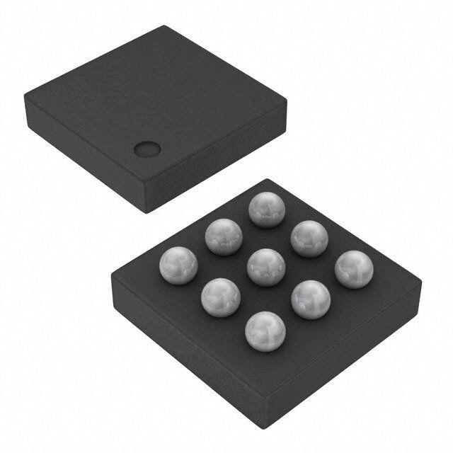
| 描述 | IC REG BUCK SYNC ADJ 0.8A 9DSBGA |
| 产品分类 | |
| 品牌 | Texas Instruments |
| 数据手册 | |
| 产品图片 |
|
| 产品型号 | TPS62651YFFR |
| PWM类型 | 电压模式 |
| rohs | 无铅 / 符合限制有害物质指令(RoHS)规范要求 |
| 产品系列 | - |
| 供应商器件封装 | 9-DSBGA(1.2x1.3) |
| 其它名称 | 296-28260-1 |
| 包装 | 剪切带 (CT) |
| 同步整流器 | 是 |
| 安装类型 | 表面贴装 |
| 封装/外壳 | 9-UFBGA,DSBGA |
| 工作温度 | -40°C ~ 85°C |
| 标准包装 | 1 |
| 电压-输入 | 2.3 V ~ 5.5 V |
| 电压-输出 | 0.75 V ~ 1.44 V |
| 电流-输出 | 800mA |
| 类型 | 降压(降压) |
| 输出数 | 1 |
| 输出类型 | 可调式 |
| 频率-开关 | 6MHz |


- 商务部:美国ITC正式对集成电路等产品启动337调查
- 曝三星4nm工艺存在良率问题 高通将骁龙8 Gen1或转产台积电
- 太阳诱电将投资9.5亿元在常州建新厂生产MLCC 预计2023年完工
- 英特尔发布欧洲新工厂建设计划 深化IDM 2.0 战略
- 台积电先进制程称霸业界 有大客户加持明年业绩稳了
- 达到5530亿美元!SIA预计今年全球半导体销售额将创下新高
- 英特尔拟将自动驾驶子公司Mobileye上市 估值或超500亿美元
- 三星加码芯片和SET,合并消费电子和移动部门,撤换高东真等 CEO
- 三星电子宣布重大人事变动 还合并消费电子和移动部门
- 海关总署:前11个月进口集成电路产品价值2.52万亿元 增长14.8%


PDF Datasheet 数据手册内容提取
TPS62650 CSP-9 TPS62651 www.ti.com SLVS808B–AUGUST2009–REVISEDJULY2011 800-mA, 6-MHz HIGH-EFFICIENCY STEP-DOWN CONVERTER 2 TM WITH I C COMPATIBLE INTERFACE IN CHIP SCALE PACKAGING CheckforSamples:TPS62650,TPS62651 FEATURES DESCRIPTION 1 • 86%Efficiencyat6MHzOperation The TPS6265x device is a high-frequency 2 synchronous step-down dc-dc converter optimized for • 38μAQuiescentCurrent battery-powered portable applications. Intended for • WideVINRangeFrom2.3Vto5.5V low-power applications, the TPS6265x supports up to • 6MHzRegulatedFrequencyOperation 800mA load current and allows the use of small, low costinductorsandcapacitors. • Best-In-ClassLoadandLineTransient • ±2%PWMDCVoltageAccuracy The device is ideal for mobile phones and similar portable applications powered by a single-cell Li-Ion • AutomaticPFM/PWMModeSwitching battery. With an output voltage range adjustable via • LowRippleLight-LoadPFM I2C interface down to 0.75V, the device supports • I2CCompatibleInterfaceupto3.4Mbps low-voltage DSPs and processors core power suppliesinsmart-phonesandhandheldcomputers. • Pin-SelectableOutputVoltage(VSEL) • InternalSoft-Start,<150-μsStart-UpTime The TPS6265x operates at a regulated 6MHz switching frequency and enters the efficiency • CurrentOverloadandThermalShutdown optimized power-save mode operation at light load Protection currents to maintain high efficiency over the entire • ThreeSurface-MountExternalComponents load current range. In the shutdown mode, the Required(OneMLCCInductor,TwoCeramic currentconsumptionisreducedtolessthan3.5μA. Capacitors) The serial interface is compatible with Standard, • CompleteSub1-mmComponentProfile Fast/Fast Plus and High-Speed mode I2C Solution specification allowing transfers at up to 3.4 Mbps. • TotalSolutionSize<13mm2 This communication interface is used for dynamic voltage scaling with voltage steps down to 12.5mV, • Availableina9-PinNanoFree™(CSP) for setting the output voltage or reprogramming the Packaging mode of operation (PFM/PWM or Forced PWM) for instance. APPLICATIONS The TPS6265x is available in an 9-pin chip-scale • SmartReflex™CompliantPowerSupply package(CSP). • OMAP™ApplicationProcessorCoreSupply • CellPhones,Smart-Phones • MicroDC-DCConverterModules spacer TPS62650 100 VI VIN FB 90 VO= 1.2V VPFI=M 2/P.7WVM Operation C1 SW VO 80 2.3 V .. 5.5 V 4.7mF 0.4L71mH C2 % 70 GND 4.7mF −y 60 c VO= FloVoOr= Roof EVNSEL Efficien 345000 VI= 4.2VVPFIM= /3P.6WVM Operation VI= 3.6V I2CBus SDA 20 PFM/PWM Operation Forced PWM Operation up to 3.4 Mbips SCL 10 0 0.1 1 10 100 1000 I −Load Current−mA O Figure1.TypicalApplication Figure2.EfficiencyvsLoadControl 1 Pleasebeawarethatanimportantnoticeconcerningavailability,standardwarranty,anduseincriticalapplicationsofTexas Instrumentssemiconductorproductsanddisclaimerstheretoappearsattheendofthisdatasheet. NanoFree,SmartReflex,OMAParetrademarksofTexasInstruments. 2 PRODUCTIONDATAinformationiscurrentasofpublicationdate. Copyright©2009–2011,TexasInstrumentsIncorporated Products conform to specifications per the terms of the Texas Instruments standard warranty. Production processing does not necessarilyincludetestingofallparameters.
TPS62650 TPS62651 SLVS808B–AUGUST2009–REVISEDJULY2011 www.ti.com Thesedeviceshavelimitedbuilt-inESDprotection.Theleadsshouldbeshortedtogetherorthedeviceplacedinconductivefoam duringstorageorhandlingtopreventelectrostaticdamagetotheMOSgates. ORDERINGINFORMATION NUPMABRETR(1) OUTPRUATNVGOEL(2T)AGE OUTPDUETFVAOULLTTAGE(2) I2CADDRESSBITS(2) PACKAGE(3) ORDERING PMAACRKKAINGGE VSEL0 VSEL1 A2 A1 (CC) TPS62650(4) 0.75Vto1.4375V 1.05V 1.2V 0 1 YFF-9 TPS62650YFF GJ TPS62651(4) 0.75Vto1.4375V 0.95V 1.1V 1 1 YFF-9 TPS62651YFF GK (1) Alldevicesarespecifiedforoperationinthecommercialtemperaturerange,–40°Cto85°C. (2) Forcustomizedoutputvoltagelimits(withina0.75Vto1.5375Vrange),defaultoutputvoltageandI2Caddress,contactthefactory. Internaltappointsareavailabletofacilitatedefaultoutputvoltagesettingsinmultiplesof50mV. (3) Forthemostcurrentpackageandorderinginformation,seethePackageOptionAddendumattheendofthisdocument,orseetheTI websiteatwww.ti.com. (4) ThefollowingregistersbitsaresetbyinternalhardwarelogicandnotuserprogrammablethroughI2C: (a)VSEL0[7]=1 (b)VSEL1[7]=1 (c)CONTROL1[3:2]=00 ABSOLUTE MAXIMUM RATINGS overoperatingfree-airtemperaturerange(unlessotherwisenoted)(1) VALUE UNIT MIN MAX atVIN,SW(2) –0.3 7 V InputVoltage atFB (2) –0.3 3.6 V atEN,VSEL,SCL,SDA (2) –0.3 V +0.3 V I Powerdissipation Internallylimited Operatingjunctiontemperature,T (3) –40 85 °C A MaximumoperatingjunctionTemperature,T 150 °C J Storagetemperaturerange,T –65 150 °C stg Humanbodymodel 2 kV ESDrating(4) Chargedevicemodel 1 kV Machinemodel 200 V (1) Stressesbeyondthoselistedunderabsolutemaximumratingsmaycausepermanentdamagetothedevice.Thesearestressratings onlyandfunctionaloperationofthedeviceattheseoranyotherconditionsbeyondthoseindicatedunderrecommendedoperating conditionsisnotimplied.Exposuretoabsolute-maximum-ratedconditionsforextendedperiodsmayaffectdevicereliability. (2) Allvoltagevaluesarewithrespecttonetworkgroundterminal. (3) Inapplicationswherehighpowerdissipationand/orpoorpackagethermalresistanceispresent,themaximumambienttemperaturemay havetobederated.Maximumambienttemperature(T )isdependentonthemaximumoperatingjunctiontemperature(T ),the A(max) J(max) maximumpowerdissipationofthedeviceintheapplication(P ),andthejunction-to-ambientthermalresistanceofthepart/package D(max) intheapplication(θ ),asgivenbythefollowingequation:T =T –(θ XP ).Toachieveoptimumperformance,itis JA A(max) J(max) JA D(max) recommendedtooperatethedevicewithamaximumjunctiontemperatureof105°C. (4) Thehumanbodymodelisa100-pFcapacitordischargedthrougha1.5-kΩresistorintoeachpin.Themachinemodelisa200-pF capacitordischargeddirectlyintoeachpin. DISSIPATION RATINGS(1) PACKAGE R (2) R (2) POWERRATING DERATINGFACTOR θJA θJB T ≤25°C ABOVET =25°C A A YFF 105°C/W 35°C/W 950mW 8mW/°C (1) MaximumpowerdissipationisafunctionofT(max),θ andT .Themaximumallowablepowerdissipationatanyallowableambient J JA A temperatureisP =[T(max)–T ]/θ . D J A JA (2) Thisthermaldataismeasuredwithhigh-Kboard(4layersboardaccordingtoJESD51-7JEDECstandard). 2 Copyright©2009–2011,TexasInstrumentsIncorporated
TPS62650 TPS62651 www.ti.com SLVS808B–AUGUST2009–REVISEDJULY2011 ELECTRICAL CHARACTERISTICS MinimumandmaximumvaluesareatV =2.3Vto5.5V,V =1.2V,EN=1.8V,EN_DCDCbit=1,AUTOmodeand I O T =-40°Cto85°C;CircuitofParameterMeasurementInformationsection(unlessotherwisenoted).Typicalvaluesareat A V =3.6V,V =1.2V,EN=1.8V,EN_DCDCbit=1,AUTOmodeandT =25°C(unlessotherwisenoted). I O A PARAMETER TESTCONDITIONS MIN TYP MAX UNIT SUPPLYCURRENT VI Inputvoltagerange 2.3 5.5 V VI=3.6V,IO=0mA,-40°C≤TJ≤85°C.Devicenotswitching 38 58 μA IQ Operatingquiescentcurrent VI=3.6V,IO=0mA.PWMmode 5.35 mA VI=3.6V,EN=GND,EN_DCDCbit=X,-40°C≤TJ≤85°C 0.5 3.5 μA I(SD) Shutdowncurrent VI=3.6V,EN=VI,EN_DCDCbit=0,-40°C≤TJ≤85°C 0.5 3.5 μA UVLO Undervoltagelockoutthreshold 2.05 2.15 V ENABLE,VSEL,SDA,SCL VIH High-levelinputvoltage 0.9 V VIL Low-levelinputvoltage 0.4 V Ilkg Inputleakagecurrent InputtiedtoGNDorVI,-40°C≤TJ≤85°C 0.01 0.7 μA POWERSWITCH VI=V(GS)=3.6V 255 rDS(on) P-channelMOSFETonresistance mΩ VI=V(GS)=2.5V 335 Ilkg P-channelleakagecurrent,PMOS V(DS)=5.5V,-40°C≤TJ≤85°C 1 μA VI=V(GS)=3.6V 140 rDS(on) N-channelMOSFETonresistance mΩ VI=V(GS)=2.5V 200 Ilkg N-channelleakagecurrent,NMOS V(DS)=5.5V,-40°C≤TJ≤85°C 1 μA Dischargeresistorforpower-down rDIS sequence 15 50 Ω P-MOScurrentlimit 2.3V≤VI≤4.8V.Openloop 1350 1500 1700 mA Inputcurrentlimitundershort-circuit conditions VO=0V 11 mA Thermalshutdown 140 °C Thermalshutdownhysteresis 15 °C OSCILLATOR fSW Oscillatorfrequency IO=0mA.PWMmode 5.4 6 6.6 MHz OUTPUT 2.3V≤VI≤5.5V,0mA≤IO(DC)≤800mA VO=0.75V,1.05V,1.20V,1.4375V(TPS62650) –2% 2% VO=0.75V,0.95V,1.10V,1.4375V(TPS62651) RegulatedDCoutput PWMoperation voltageaccuracy 2.3V≤VI≤5.5V,0mA≤IO(DC)≤800mA VO=0.75V,1.05V,1.20V,1.4375V(TPS62650) –2% 3% VO TPS62650/1 VO=0.75V,0.95V,1.10V,1.4375V(TPS62651) PFM/PWMOperation RegulatedDCoutput VI=3.6V,VO=1.20V,IO(DC)=50mA -0.5% +0.5% voltagetemperaturedrift -40°C≤TJ≤105°C.PWMoperation Lineregulation VI=VO+0.5V(min2.3V)to5.5V,IO(DC)=200mA 0.13 %/V Loadregulation IO(DC)=0mAto800mA –0.00046 %/mA Feedbackinputresistance 480 kΩ VPOFM=1o.p0e5raVti,oVnSEL=GND,IO(DC)=1mA 16 mVPP ΔVO Power-savemoderipplevoltage VPOFM=1o.p2e0raVti,oVnSEL=VI,IO(DC)=1mA 16 mVPP DAC TPS62650 Resolution 6 Bits TPS62651 Differentialnonlinearity Specifiedmonotonicbydesign ±0.4 LSB Copyright©2009–2011,TexasInstrumentsIncorporated 3
TPS62650 TPS62651 SLVS808B–AUGUST2009–REVISEDJULY2011 www.ti.com ELECTRICAL CHARACTERISTICS (continued) MinimumandmaximumvaluesareatV =2.3Vto5.5V,V =1.2V,EN=1.8V,EN_DCDCbit=1,AUTOmodeand I O T =-40°Cto85°C;CircuitofParameterMeasurementInformationsection(unlessotherwisenoted).Typicalvaluesareat A V =3.6V,V =1.2V,EN=1.8V,EN_DCDCbit=1,AUTOmodeandT =25°C(unlessotherwisenoted). I O A PARAMETER TESTCONDITIONS MIN TYP MAX UNIT TIMING SetupTimeBetween RisingENandStartof TPS62650/1 50 μs I2CStream Outputvoltagesettling Frommintomaxoutputvoltage, VO time TPS62650/1 IO(DC)=500mA,VSEL=VI,PWMoperation 12 μs TimefromactiveENtoVO 125 VO=1.2V,IO=0mA,PWMoperation Start-uptime TPS62650/1 μs TimefromactiveENtoVO 120 VO=1.05V,IO=0mA,PFMoperation I2C INTERFACE TIMING CHARACTERISTICS(1) PARAMETER TESTCONDITIONS MIN MAX UNIT Standardmode 100 kHz Fastmode 400 kHz Fastmodeplus 1 MHz f SCLClockFrequency High-speedmode(writeoperation),C –100pFmax 3.4 MHz (SCL) B High-speedmode(readoperation),C –100pFmax 3.4 MHz B High-speedmode(writeoperation),C –400pFmax 1.7 MHz B High-speedmode(readoperation),C –400pFmax 1.7 MHz B Standardmode 4.7 μs BusFreeTimeBetweenaSTOPand t Fastmode 1.3 μs BUF STARTCondition Fastmodeplus 0.5 μs Standardmode 4 μs HoldTime(Repeated)START Fastmode 600 ns t ,t HD STA Condition Fastmodeplus 260 ns High-speedmode 160 ns Standardmode 4.7 μs Fastmode 1.3 μs t LOWPeriodoftheSCLClock Fastmodeplus 0.5 μs LOW High-speedmode,C –100pFmax 160 ns B High-speedmode,C –400pFmax 320 ns B Standardmode 4 μs Fastmode 600 ns t HIGHPeriodoftheSCLClock Fastmodeplus 260 ns HIGH High-speedmode,C –100pFmax 60 ns B High-speedmode,C –400pFmax 120 ns B Standardmode 4.7 μs SetupTimeforaRepeatedSTART Fastmode 600 ns t ,t SU STA Condition Fastmodeplus 260 ns High-speedmode 160 ns Standardmode 250 ns Fastmode 100 ns t ,t DataSetupTime SU DAT Fastmodeplus 50 ns High-speedmode 10 ns (1) Specifiedbydesign.Nottestedinproduction. 4 Copyright©2009–2011,TexasInstrumentsIncorporated
TPS62650 TPS62651 www.ti.com SLVS808B–AUGUST2009–REVISEDJULY2011 I2C INTERFACE TIMING CHARACTERISTICS(1) (continued) PARAMETER TESTCONDITIONS MIN MAX UNIT Standardmode 0 3.45 μs Fastmode 0 0.9 μs t ,t DataHoldTime Fastmodeplus 0 μs HD DAT High-speedmode,C –100pFmax 0 70 ns B High-speedmode,C –400pFmax 0 150 ns B Standardmode 20+0.1C 1000 ns B Fastmode 20+0.1C 300 ns B t RiseTimeofSCLSignal Fastmodeplus 120 ns RCL High-speedmode,C –100pFmax 10 40 ns B High-speedmode,C –400pFmax 20 80 ns B Standardmode 20+0.1C 1000 ns B Fastmode 20+0.1C 300 ns RiseTimeofSCLSignalAftera B t RepeatedSTARTConditionandAfter Fastmodeplus 120 ns RCL1 anAcknowledgeBIT High-speedmode,C –100pFmax 10 80 ns B High-speedmode,C –400pFmax 20 160 ns B Standardmode 20+0.1C 300 ns B Fastmode 20+0.1C 300 ns B t FallTimeofSCLSignal Fastmodeplus 120 ns FCL High-speedmode,C –100pFmax 10 40 ns B High-speedmode,C –400pFmax 20 80 ns B Standardmode 20+0.1C 1000 ns B Fastmode 20+0.1C 300 ns B t RiseTimeofSDASignal Fastmodeplus 120 ns RDA High-speedmode,C –100pFmax 10 80 ns B High-speedmode,C –400pFmax 20 160 ns B Standardmode 20+0.1C 300 ns B Fastmode 20+0.1C 300 ns B t FallTimeofSDASignal Fastmodeplus 120 ns FDA High-speedmode,C –100pFmax 10 80 ns B High-speedmode,C –400pFmax 20 160 ns B Standardmode 4 μs Fastmode 600 ns t t SetupTimeofSTOPCondition SU, STO Fastmodeplus 260 ns High-Speedmode 160 ns Standardmode 400 pF Fastmode 400 pF C CapacitiveLoadforSDAandSCL B Fastmodeplus 550 pF High-Speedmode 400 pF Copyright©2009–2011,TexasInstrumentsIncorporated 5
TPS62650 TPS62651 SLVS808B–AUGUST2009–REVISEDJULY2011 www.ti.com I2C TIMING DIAGRAMS SDA tf tLOW tr tsu;DAT tf thd;STA tr tBUF SCL thd;STA tsu;STA tsu;STO S thd;DAT HIGH Sr P S Figure3. SerialInterfaceTimingDiagramforStandard-,Fast-,Fast-ModePlus Sr Sr P tfDA trDA SDAH thd;DAT tsu;STO tsu;STA thd;STA tsu;DAT SCLH tfCL trCL1 trCL trCL1 See Note A tHIGH tLOW tLOW tHIGH See Note A = MCS Current Source Pull-Up = R(P) Resistor Pull-Up Note A: First rising edge of the SCLH signal after Sr and after each acknowledge bit. Figure4. SerialInterfaceTimingDiagramforHS-Mode 6 Copyright©2009–2011,TexasInstrumentsIncorporated
TPS62650 TPS62651 www.ti.com SLVS808B–AUGUST2009–REVISEDJULY2011 PIN ASSIGNMENTS TPS6265x TPS6265x CSP−9 CSP−9 (TOPVIEW) (BOTTOM VIEW) A1 A2 A3 A3 A2 A1 B1 B2 B3 B3 B2 B1 C1 C2 C3 C3 C2 C1 TERMINALFUNCTIONS TERMINAL I/O DESCRIPTION NAME NO. VIN A2 I Thisistheinputvoltagepinofthedevice.Connectdirectlytotheinputbypasscapacitor. Thisistheenablepinofthedevice.Connectthispintogroundforcesthedeviceinto shutdownmode.PullingthispintoV enablesthedevice.Ontherisingedgeoftheenable EN B3 I I pin,alltheregistersareresetwiththeirdefaultvalues.Thispinmustnotbeleftfloatingand mustbeterminated. VSELsignalisprimarilyusedtoscaletheoutputvoltageandtosettheTPS6265xoperation betweenactivemode(VSEL=HIGH)andsleepmode(VSEL=LOW).Themodeofoperation VSEL A1 I canalsobeadaptedbyI2Csettings.Thispinmustnotbeleftfloatingandmustbe terminated. SDA A3 I/O Serialinterfaceaddress/dataline. SCL B2 I Serialinterfaceclockline. FB C1 I Outputfeedbacksenseinput.ConnectFBtotheconverteroutput. GND C2,C3 Ground. Thisistheswitchpinoftheconverterandconnectedtothedrainoftheinternalpower SW B1 I/O MOSFETs. FUNCTIONAL BLOCK DIAGRAM EN VIN Undervoltage VIN Lockout Bias Supply Soft-Start Negative Inductor Current Detect Bandgap VREF=0.75V Power Save Mode Switching Logic Thermal Current Limit Shutdown Detect Frequency Control FB - Gate Driver SW Anti Shoot-Through + SDA I2C I/F CLoongtircol 6-Bit SCL Registers DAC VDAC GGGNNNDDD VSEL Copyright©2009–2011,TexasInstrumentsIncorporated 7
TPS62650 TPS62651 SLVS808B–AUGUST2009–REVISEDJULY2011 www.ti.com PARAMETER MEASUREMENT INFORMATION TPS62650 V VIN FB I V C1 SW O L1 GND C2 GND EN V = Roof O VSEL VO= Floor L= muRata LQM21PN1R0NGR C1 = muRata GRM155R60J475M (4.7mF, 6.3V, 0402, X5R) I2CBus SDA C2 = muRata GRM155R60J475M (4.7mF, 6.3V, 0402, X5R) up to 3.4 Mbps SCL Note:The internal registers are set to their default values TYPICAL CHARACTERISTICS Table of Graphs FIGURE vsOutputcurrent 5,6,7,8 η Efficiency vsInputvoltage 9 Peak-to-peakoutputripple vsOutputCurrent 10,11,12,13 voltage vsOutputcurrent 14,15,16,17 V DCoutputvoltage O vsAmbienttemperature 18,19 Measuredoutputvoltage vsDACtargetoutputvoltage 20 PFM/PWMBoundaries 21 I Quiescentcurrent vsInputvoltage 22 Q I Shutdowncurrent vsInputvoltage 23 SD f Switchingfrequency vsInputvoltage 24 S P-channelMOSFETr vsInputvoltage 25 DS(on) r DS(on) N-channelMOSFETr vsInputvoltage 26 DS(on) Loadtransientresponse 27-38 LinetransientPWMoperation 39 Combinedlineandloadtransient 40 response PWMoperation 41 Power-savemodeoperation 42 Dynamicvoltagemanagement 43,44 Outputvoltagerampcontrol 45 Start-up 46,47 8 Copyright©2009–2011,TexasInstrumentsIncorporated
TPS62650 TPS62651 www.ti.com SLVS808B–AUGUST2009–REVISEDJULY2011 TYPICAL CHARACTERISTICS (continued) EFFICIENCY EFFICIENCY vs vs OUTPUTCURRENT OUTPUTCURRENT 100 100 VI= 2.7 V VO= 1.20 V VO= 1.05 V VI= 2.7 V 90 PFM/PWM 90 PFM/PWM 80 80 70 VI= 3.6 V 70 VI= 3.6 V % 60 PFM/PWM % 60 PFM/PWM ncy - 50 ncy - 50 VI= 4.2 V cie VI= 4.2 V cie PFM/PWM Effi 40 PFM/PWM Effi 40 30 30 V = 3.6 V I 20 Forced PWM 20 10 10 0 0 0.1 1 10 100 1000 0.1 1 10 100 1000 IO- Output Current - mA IO- Output Current - mA Figure5. Figure6. EFFICIENCY EFFICIENCY vs vs OUTPUTCURRENT OUTPUTCURRENT 100 100 V = 1.4375 V V = 0.75 V O O 90 90 V = 2.7 V I 80 80 PFM/PWM V = 2.7 V 70 I 70 PFM/PWM V = 3.6 V % 60 V = 3.6 V % 60 I y - PFIM/PWM y - PFM/PWM nc 50 nc 50 e e Effici 40 PVFIM= /4P.W2 VM Effici 40 VI= 4.2 V PFM/PWM 30 30 20 20 10 10 0 0 0.1 1 10 100 1000 0.1 1 10 100 1000 IO- Output Current - mA IO- Output Current - mA Figure7. Figure8. Copyright©2009–2011,TexasInstrumentsIncorporated 9
TPS62650 TPS62651 SLVS808B–AUGUST2009–REVISEDJULY2011 www.ti.com TYPICAL CHARACTERISTICS (continued) EFFICIENCY PEAK-TO-PEAKOUTPUTRIPPLEVOLTAGE vs vs INPUTVOLTAGE OUTPUTCURRENT 100 24 98 VO= 1.2 V V 22 VO= 1.2 V PFM/PWM m 96 e - 20 94 g a 92 olt 18 VI= 4.8 V V % 90 IO= 100 mA ple 16 VI= 3.6 V ciency - 888468 IO= 300 mAIO= 10 mA utput Rip 1124 VI= 2.5 V Effi 82 k O 10 a 80 e 8 P 78 IO= 1 mA k-to- 6 76 a e 4 74 - P O 2 72 V 70 0 2.3 2.7 3.1 3.5 3.9 4.3 4.7 5.1 5.5 0 100 200 300 400 500 600 700 800 VI- Input Voltage - V IO- Load Current - mA Figure9. Figure10. PEAK-TO-PEAKOUTPUTRIPPLEVOLTAGE PEAK-TO-PEAKOUTPUTRIPPLEVOLTAGE vs vs OUTPUTCURRENT OUTPUTCURRENT 24 24 mV 22 VO= 1.05 V mV 22 VO= 0.75 V e - 20 e - 20 g g olta 18 VI= 4.8 V olta 18 VI= 4.8 V V V ple 16 VI= 3.6 V ple 16 VI= 3.6 V p p put Ri 1124 VI= 2.5 V put Ri 1124 VI= 2.5 V ut ut O 10 O 10 k k a a e 8 e 8 P P o- o- k-t 6 k-t 6 a a e 4 e 4 P P - - O 2 O 2 V V 0 0 0 100 200 300 400 500 600 700 800 0 100 200 300 400 500 600 700 800 I - Load Current - mA I - Load Current - mA O O Figure11. Figure12. 10 Copyright©2009–2011,TexasInstrumentsIncorporated
TPS62650 TPS62651 www.ti.com SLVS808B–AUGUST2009–REVISEDJULY2011 TYPICAL CHARACTERISTICS (continued) PEAK-TO-PEAKOUTPUTRIPPLEVOLTAGE DCOUTPUTVOLTAGE vs vs OUTPUTCURRENT OUTPUTCURRENT 24 1.224 V = 1.2 V mV 22 VO= 1.4375 V O e - 20 g olta 18 VI= 4.8 V 1.212 VI= 4.8 V VI= 3.6 V ple V 16 VI= 3.6 V e - V PFM/PWM PWM Operation p g k Output Ri 111024 VI= 2.5 V Output Volta 1.2 VI= 2.5 V VI= 3.6 V ea 8 - PFM/PWM PFM/PWM P O o- V k-t 6 1.188 a e 4 P - O 2 V 0 1.176 0 100 200 300 400 500 600 700 800 0.1 1 10 100 1000 I - Load Current - mA I - Output Current - mA O O Figure13. Figure14. DCOUTPUTVOLTAGE DCOUTPUTVOLTAGE vs vs OUTPUTCURRENT OUTPUTCURRENT 1.071 0.765 VO= 1.05 V VO= 0.75 V V = 4.8 V I V = 3.6 V PFM/PWM I 1.061 VI= 4.8 V 0.758 PFM/PWM e - V PFM/PWM PVFIM= /3P.W6 VM e - V g g a a olt olt ut V 1.05 ut V 0.75 VI= 2.5 V p p PFM/PWM ut V = 2.5 V ut O I O - PFM/PWM - O O V V 1.04 0.743 1.029 0.735 0.1 1 10 100 1000 0.1 1 10 100 1000 I - Output Current - mA I - Output Current - mA O O Figure15. Figure16. Copyright©2009–2011,TexasInstrumentsIncorporated 11
TPS62650 TPS62651 SLVS808B–AUGUST2009–REVISEDJULY2011 www.ti.com TYPICAL CHARACTERISTICS (continued) DCOUTPUTVOLTAGE DCOUTPUTVOLTAGE vs vs OUTPUTCURRENT AMBIENTTEMPERATURE 1.466 1.212 V = 1.4375 V V = 1.2 V, O O I = 250 mA, 1.209 O PWM Operation ge - V 1.452 PVFIM= /4P.W8 VM PWVMI =O p3e.6r aVtion ge - V 11..220036 VI= 4.2 V VI= 3.6 V ut Volta 1.438 ut Volta 1.2 p p Out V = 2.5 V Out 1.197 VI= 2.7 V V- O PFIM/PWM VI= 3.6 V V- O 1.423 PFM/PWM 1.194 1.191 1.409 1.188 0.1 1 10 100 1000 -40 -20 0 20 40 60 80 100 IO- Output Current - mA TA-Ambient Temperature - °C Figure17. Figure18. DCOUTPUTVOLTAGE MEASUREDOUTPUTVOLTAGE vs vs AMBIENTTEMPERATURE DACTARGETOUTPUTVOLTAGE 1.061 4 VO= 1.05 V, VI= 3.6 V, TA= 85°C 1.058 VI= 4.2 V IO= 250 mA, 3 IO= 100 mA, PWM Operation V PWM Operation m ge - V 11..005535 VI= 3.6 V VI= 2.7 V Voltage -oltage - 2 TA= 25°C olta put ut V 1 Output V 1.10.4075 ured Outget Outp 0 V- O MeasC Tar -1 1.045 A D -2 T = -40°C 1.042 A 1.04 -3 -40 -20 0 20 40 60 80 100 0.75 0.85 0.95 1.05 1.15 1.25 1.35 1.45 T -Ambient Temperature - °C V - DAC Target Output Voltage - V A O Figure19. Figure20. 12 Copyright©2009–2011,TexasInstrumentsIncorporated
TPS62650 TPS62651 www.ti.com SLVS808B–AUGUST2009–REVISEDJULY2011 TYPICAL CHARACTERISTICS (continued) QUIESCENTCURRENT vs PFM/PWMBOUNDARIES INPUTVOLTAGE 220 55 220100 VO = 1.2 V Always PWM 50 TA= 85oC 190 180 45 A 116700 Am 40 TA= 25oC m 150 − − 140 nt 35 e nt 130 PFM to PWM rr ad Curre 11120910000 Mode Change scent Cu 2350 T = -40oC Lo 80 The switching mode uie 20 A − 70 Q changes at these borders IO 60 − 15 50 Q I 40 PWM to PFM 10 30 Mode Change 20 5 10 Always PFM 0 0 2.5 2.7 2.93.13.33.5 3.7 3.9 4.14.34.54.7 4.9 5.15.35.5 2.5 2.7 2.9 3.13.3 3.5 3.73.9 4.14.34.54.7 4.9 5.1 5.35.5 VI−Input Voltage−V VI−Input Voltage−V Figure21. Figure22. SHUTDOWNCURRENT SWITCHINGFREQUENCY vs vs INPUTVOLTAGE INPUTVOLTAGE 2500 7 T = 85oC A I = 50 mA 2250 O 6.5 2000 A z n H 6 rrent−11570500 ncy - M 5.5 IIOO== 135000 mmAA u e I = 400 mA C u O wn 1250 req 5 IO= 500 mA do g F IO= 600 mA hut1000 T = 25oC hin 4.5 IO= 700 mA S A c − 750 wit IO= 800 mA SD) - S 4 I( 500 fs 3.5 250 T = -40oC A 0 3 2.5 2.7 2.9 3.13.33.53.7 3.94.1 4.34.5 4.74.9 5.15.35.5 2.3 2.7 3.1 3.5 3.9 4.3 4.7 5.1 5.5 VI−Input Voltage−V VI- Input Voltage - V Figure23. Figure24. Copyright©2009–2011,TexasInstrumentsIncorporated 13
TPS62650 TPS62651 SLVS808B–AUGUST2009–REVISEDJULY2011 www.ti.com TYPICAL CHARACTERISTICS (continued) r P-MOSFET r N-MOSFET DS(on) DS(on) vs vs INPUTVOLTAGE INPUTVOLTAGE 450 300 Wm 425 PWM Mode Operation Wm PWM Mode Operation e - 400 e - 275 c c n n 250 sta 375 TA= 85°C sta TA= 85°C esi 350 esi 225 R R n- 325 TA= 25°C n- O O 200 T = 25°C e 300 e A c c ur ur 175 o 275 o S S n- 250 n- 150 ai ai c Dr 225 c Dr 125 ati 200 ati St St 100 - S(on) 115705 TA= -40°C - S(on) 75 TA= -40°C D D r 125 r 50 2.5 2.9 3.3 3.7 4.1 4.5 4.9 5.3 2.5 2.9 3.3 3.7 4.1 4.5 4.9 5.3 V - Input Voltage - V V - Input Voltage - V I I Figure25. Figure26. LOADTRANSIENT:50mA/400mA/50mA LOADTRANSIENT:50mA/400mA PWMOPERATION PWMOPERATION V = 3.6 V I v v di di VO= 1.35 V A/ A/ IOm IOm 0 0 0 0 2 2 et et s s Off Off V V 0- 0- 2 2 VO1. VO1. - - v v di di mV/ VI= 3.6 V mV/ 0 VO= 1.20 V 0 2 2 t−Time = 5ms/div t−Time = 1ms/div Figure27. Figure28. 14 Copyright©2009–2011,TexasInstrumentsIncorporated
TPS62650 TPS62651 www.ti.com SLVS808B–AUGUST2009–REVISEDJULY2011 TYPICAL CHARACTERISTICS (continued) LOADTRANSIENT:400mA/50mA LOADTRANSIENT:50mA/400mA/50mA PWMOPERATION PFM/PWMOPERATION V = 3.6 V I div VO= 1.20 V div IOmA/ IOmA/ 0 0 0 0 2 2 et et s s Off Off V V 0- 0- 2 2 VO1.- VO1.- v v di di V/ V/ VI= 3.6 V m m V = 1.20 V 0 0 O 2 2 t−Time = 1ms/div t−Time = 10ms/div Figure29. Figure30. LOADTRANSIENT:50mA/400mA LOADTRANSIENT:400mA/50mA PFM/PWMOPERATION PFM/PWMOPERATION v VI= 3.6 V v VI= 3.6 V A/di VO= 1.20 V A/di VO= 1.20 V IOm IOm 0 0 0 0 2 2 et et s s Off Off V V 0- 0- 2 2 VO1. VO1. - - v v di di V/ V/ m m 0 0 2 2 t−Time = 1ms/div t−Time = 1ms/div Figure31. Figure32. Copyright©2009–2011,TexasInstrumentsIncorporated 15
TPS62650 TPS62651 SLVS808B–AUGUST2009–REVISEDJULY2011 www.ti.com TYPICAL CHARACTERISTICS (continued) LOADTRANSIENT:400mA/750mA/400mA LOADTRANSIENT:400mA/750mA PWMOPERATION PWMOPERATION et et s s V = 3.6 V Off Off VI = 1.20 V A A O m m 0 0 0 0 O4 O4 I - I - v v di di A/ A/ m m 0 0 0 0 2 2 et et s s Off Off V V 0- 0- 2 2 VO1. VO1. - - v v V/di VI= 3.6 V V/di m V = 1.20 V m 0 O 0 2 2 t−Time = 5ms/div t−Time = 1ms/div Figure33. Figure34. LOADTRANSIENT:750mA/400mA LOADTRANSIENT:5mA/100mA/5mA PWMOPERATION PFM/PWMOPERATION set V = 3.6 V VI= 3.6 V Off VI = 1.20 V VO= 1.05 V A O m v 0 di O40 OA/ I - Im v 0 di 5 A/ m 0 0 2 et et s s Off Off V V 0- 5- 2 0 VO1. VO1. - - v v di di V/ V/ m m 0 0 2 1 t−Time = 1ms/div t−Time = 250ms/div Figure35. Figure36. 16 Copyright©2009–2011,TexasInstrumentsIncorporated
TPS62650 TPS62651 www.ti.com SLVS808B–AUGUST2009–REVISEDJULY2011 TYPICAL CHARACTERISTICS (continued) LOADTRANSIENT:5mA/100mA LOADTRANSIENT:100mA/5mA PFM/PWMOPERATION PFM/PWMOPERATION VI= 3.6 V VI= 3.6 V div VO= 1.05 V div VO= 1.05 V IOmA/ IOmA/ 0 0 0 0 1 1 v v di di A/ A/ ILm ILm 0 0 0 0 2 2 et et s s Off Off V V 5- 5- 0 0 VO1. VO1. - - v v di di V/ V/ m m 0 0 1 t−Time = 2.5ms/div 1 t−Time = 2.5ms/div Figure37. Figure38. COMBINEDLINE/LOADTRANSIENT LINETRANSIENT (3.3VTO3.9V,400mATO800mA) PWMOPERATION PWMOPERATION set VO= 1.20 V, IO= 50mA set Off PWM Mode Off IO V V 500 mA/div 3- 3- 3. 3. VI- VI- V/div V/div 500 mVVI /div m m 0 0 0 0 5 5 et et s s Off Off V V 0- 0- 2 2 VO1. VO1. - - V = 1.20 V v v O di di PWM Mode V/ V/ m m 10 t−Time = 50ms/div 20 t−Time = 25ms/div Figure39. Figure40. Copyright©2009–2011,TexasInstrumentsIncorporated 17
TPS62650 TPS62651 SLVS808B–AUGUST2009–REVISEDJULY2011 www.ti.com TYPICAL CHARACTERISTICS (continued) PWMOPERATION POWERSAVEMODEOPERATION v di A/ IL100 m VI= 3.6 V, VO= 1.20 V A/div IO= 200 mA IL0 m 0 v 1 Wdi SV/ 2 et s set Off V Off 20-V VO-1.20- VO-div1. VI= 3.6 V div mV/ VO= 1.20 V mV/ 10 IO= 30 mA 0 1 t−Time = 40 ns/div t−Time = 500 ns/div Figure41. Figure42. DYNAMICVOLTAGEMANAGEMENT DYNAMICVOLTAGEMANAGEMENT VI= 3.6 V ELdiv ELdiv VO= 1.05 V (PFM)/ 1.20 V (PWM) VS2V/ VO= 1.20 V VS2V/ VO= 1.20 V Offset Offset V V VO1.05-- PWM VO= 1.05 V VO1.05-- PWM V/div PFM V/div PFM VO= 1.05 V m m 50 50 v v di di ILmA/ ILmA/ 200 VVIO== 3 1.6.0 V5 V (PFM)/ 1.20 V (PWM) RL= 5W 200 RL= 270W t−Time = 5ms/div t−Time = 25ms/div Figure43. Figure44. 18 Copyright©2009–2011,TexasInstrumentsIncorporated
TPS62650 TPS62651 www.ti.com SLVS808B–AUGUST2009–REVISEDJULY2011 TYPICAL CHARACTERISTICS (continued) OUTPUTVOLTAGE RAMPCONTROL STARTUP ELdiv Ndiv SV/ EV/ V2 VI= 3.6 V 2 VI= 3.6 V VIOO== 0 0 m.7A5 V/ 1.4375 V (PWM) VO= 1.05 V (PFM) div IO= 0 mA OV/ VO= 1.4375 V V0 m 0 5 et s Off V 5- Slew Rate = 4.8 mV/ms 7 VOmV/div0.- IL0 mA/div 0 VO= 0.75 V 10 0 2 t−Time = 50ms/div t−Time = 20ms/div Figure45. Figure46. STARTUP v Ndi EV/ 2 V = 3.6 V I V = 1.20 V (PWM) O R = 5W L v di OV/ Vm 0 0 5 v di A/ ILm 0 0 2 t−Time = 20ms/div Figure47. Copyright©2009–2011,TexasInstrumentsIncorporated 19
TPS62650 TPS62651 SLVS808B–AUGUST2009–REVISEDJULY2011 www.ti.com DETAILED DESCRIPTION Operation The TPS6265x is a synchronous step-down converter typically operates at a regulated 6-MHz frequency pulse width modulation (PWM) at moderate to heavy load currents. At light load currents, the TPS6265x converter operates in power-save mode with pulse frequency modulation (PFM) and automatic transition into PWM operationwhentheloadcurrentincreases. The TPS6265x integrates an I2C compatible interface allowing transfers up to 3.4 Mbps. This communication interface can be used for dynamic voltage scaling with voltage steps down to 12.5 mV, for reprogramming the mode of operation (PFM or forced PWM) or disable/enabling the output voltage for instance. For more details, seetheI2Cinterfaceandregisterdescriptionsection. The converter uses a unique frequency locked ring oscillating modulator to achieve best-in-class load and line response and allows the use of tiny inductors and small ceramic input and output capacitors. At the beginning of each switching cycle, the P-channel MOSFET switch is turned on and the inductor current ramps up rising the outputvoltageuntilthemaincomparatortrips,thenthecontrollogicturnsofftheswitch. Onekeyadvantageofthenon-lineararchitectureisthatthereisnotraditionalfeed-backloop.Theloopresponse to change in V is essentially instantaneous, which explains its extraordinary transient response. The absence of O a traditional, high-gain compensated linear loop means that the TPS6265x is inherently stable over a range of smallLandC . O Although this type of operation normally results in a switching frequency that varies with input voltage and load current, an internal frequency lock loop (FLL) holds the switching frequency constant over a large range of operatingconditions. Combined with best in class load and line transient response characteristics, the low quiescent current of the device (ca. 38μA) allows to maintain high efficiency at light load, while preserving fast transient response for applicationsrequiringtightoutputregulation. SWITCHING FREQUENCY The magnitude of the internal ramp, which is generated from the duty cycle, reduces for duty cycles either set of 50%. Thus, there is less overdrive on the main comparator inputs which tends to slow the conversion down. The intrinsic maximum operating frequency of the converter is about 10MHz to 12MHz, which is controlled to circa. 6MHzbyafrequencylockedloop. When high or low duty cycles are encountered, the loop runs out of range and the conversion frequency falls below6MHz.Thetendencyisfortheconvertertooperatemoretowardsa"constantinductorpeakcurrent"rather than a "constant frequency". In addition to this behavior which is observed at high duty cycles, it is also noted at lowdutycycles. When the converter is required to operate towards the 6MHz nominal at extreme duty cycles, the application can be assisted by decreasing the ratio of inductance (L) to the output capacitor's equivalent serial inductance (ESL). This increases the ESL step seen at the main comparator's feed-back input thus decreasing its propagation delay,henceincreasingtheswitchingfrequency. POWER-SAVE MODE If the load current decreases, the converter will enter Power Save Mode operation automatically. During power-savemodetheconverteroperatesindiscontinouscurrent(DCM)single-pulsePFMmode,whichproduces lowoutputripplecomparedwithotherPFMarchitectures. When in power-save mode, the converter resumes its operation when the output voltage trips below the nominal voltage. It ramps up the output voltage with a minimum of one pulse and goes into power-save mode when the inductor current has returned to a zero steady state. The PFN on-time varies inversely proportional to the input voltageandproportionaltotheoutputvoltagegivingtheregulatedswitchingfrequencywhenissteady-state. PFM mode is left and PWM operation is entered as the output current can no longer be supported in PFM mode. As a consequence, the DC output voltage is typically positioned ca 0.5% above the nominal output voltage and thetransitionbetweenPFMandPWMisseamless. 20 Copyright©2009–2011,TexasInstrumentsIncorporated
TPS62650 TPS62651 www.ti.com SLVS808B–AUGUST2009–REVISEDJULY2011 PFM Mode at Light Load PFM Ripple Nominal DC Output Voltage PWM Mode at Heavy Load Figure48. OperationinPFMModeandTransfertoPWMMode MODE SELECTION Depending on the settings of CONTROL1 register the device can be operated in either the regulated frequency PWM mode or in the automatic PWM and power-save mode. In this mode, the converter operates in a regulated frequency PWM mode at moderate to heavy loads and in the PFM mode during light loads, which maintains high efficiencyoverawideloadcurrentrange.Formoredetails,seetheCONTROL1registerdescription. The regulated frequency PWM mode has the tightest regulation and the best line/load transient performance. Furthermore, this mode of operation allows simple filtering of the switching frequency for noise-sensitive applications.InforcedPWMmode,theefficiencyislowercomparedtothepower-savemodeduringlightloads. It is possible to switch from power-save mode (PFM) to forced PWM mode during operation either via the VSEL signal or by re-programming the CONTROL1 register. This allows adjustments to the converters operation to matchthespecificsystemrequirementsleadingtomoreefficientandflexiblepowermanagement. ENABLE The device starts operation when EN pin is set high and starts up with the soft start. This signal is gated by the EN_DCDCbitdefinedinregisterVSEL0andVSEL1.OnrisingedgeoftheENpin,alltheregistersareresetwith their default values. Enabling the converter's operation via the EN_DCDC bit does not affect internal register settings. This allows the output voltage to be programmed to other values than the default voltage before starting uptheconverter.Formoredetails,seetheVSEL0/1registerdescription. Pulling the EN pin, VSEL0[6] bit or VSEL1[6] bit low forces the device into shutdown, with a shutdown current as defined in the electrical characteristics table. In this mode, the P and N-channel MOSFETs are turned off, the internal resistor feedback divider is disconnected, and the entire internal-control circuitry is switched off. For properoperation,theENpinmustbeterminatedandmustnotbeleftfloating. In addition, depending on the setting of CONTROL2[6] bit, the device can actively discharge the output capacitor when it turns off. The integrated discharge resistor has a typical resistance of 15 Ω. The required time to dischargetheoutputcapacitoratV dependsonloadcurrentandtheoutputcapacitancevalue. O SOFT START The TPS6265x has an internal soft-start circuit that limits the inrush current during start-up. This limits input voltagedropswhenabatteryorahigh-impedancepowersourceisconnectedtotheinputoftheconverter. The soft-start system progressively increases the on-time from a minimum pulse-width of 35ns as a function of the output voltage. This mode of operation continues for c.a. 100μs after enable. Should the output voltage not havereacheditstargetvaluebythistime,suchasinthecaseofheavyload,thesoft-starttransitionstoasecond modeofoperation. The converter will then operate in a current limit mode, specifically the P-MOS current limit is set to half the nominal limit and the N-channel MOSET remains on until the inductor current has reset. After a further 100 μs, the device ramps up to full current limit operation providing that the output voltage has risen above 0.5V (approximately).Therefore,thestart-uptimedependsontheoutputcapacitorandloadcurrent. Copyright©2009–2011,TexasInstrumentsIncorporated 21
TPS62650 TPS62651 SLVS808B–AUGUST2009–REVISEDJULY2011 www.ti.com UNDERVOLTAGE LOCKOUT The undervoltage lockout circuit prevents the device from misoperation at low input voltages. It prevents the converter from turning on the switch or rectifier MOSFET under undefined conditions. The TPS6265x device have a UVLO threshold set to 2.05V (typical). Fully functional operation is permitted down to 2.15 V input voltage. SHORT-CIRCUIT PROTECTION The TPS6265x integrates a P-channel MOSFET current limit to protect the device against heavy load or short circuits. When the current in the P-channel MOSFET reaches its current limit, the P-channel MOSFET is turned off and the N-channel MOSFET is turned on. The regulator continues to limit the current on a cycle-by-cycle basis. As soon as the output voltage falls below ca. 0.4V, the converter current limit is reduced to half of the nominal value and the PWROK bit is reset. Because the short-circuit protection is enabled during start-up, the device does not deliver more than half of its nominal current limit until the output voltage exceeds approximately 0.5V. Thisneedstobeconsideredwhenaloadactingasacurrentsinkisconnectedtotheoutputoftheconverter. THERMAL SHUTDOWN As soon as the junction temperature, T , exceeds typically 140°C, the device goes into thermal shutdown. In this J mode, the P- and N-channel MOSFETs are turned off. The device continues its operation when the junction temperatureagainfallsbelowtypically130°C. VOLTAGE AND MODE SELECTION The TPS6265x features a pin-selectable output voltage. VSEL is primarily used to scale the output voltage between active (VSEL = HIGH) and sleep mode (VSEL = LOW). For maximum flexibility, it is possible to reprogram the operating mode of the converter (e.g. forced PWM, or auto transition PFM/PWM) associated with VSELsignalviatheI2Cinterface VSELoutputvoltageandmodeselectionisdefinedasfollowing: VSEL = LOW: –– DC/DC output voltage determined by VSEL0 register value. DC/DC mode of operation is determinedbyMODE0bitinCONTROL1register. VSEL = HIGH: –– DC/DC output voltage determined by VSEL1 register value. DC/DC mode of operation is determinedbyMODE1bitinCONTROL1register. The application processor programs via I2C the output voltages associated with the two states of VSEL signal: floor (VSEL0) and roof (VSEL1) values. The application processor also writes the DEFSLEW value in the CONTROL2registertocontroltheoutputvoltageramprate. These two registers can be continuously updated via I2C to provide the appropriate output voltage according to the VSEL input. The voltage changes with the selected ramp rate immediately after writing to the VSEL0 or VSEL1register. Table1showstheoutputvoltagestatesdependingonVSEL0,VSEL1registers,andVSELsignal. Table1.DynamicVoltageScalingFunctionalOverview VSELPIN VSEL0REGISTER VSEL1REGISTER OUTPUTVOLTAGE Low Noaction Noaction Floor Low Writenewvalue Noaction Changetonewvalue Low Noaction Write Nochangestaysatfloorvoltage High Noaction Noaction Roof High Writenewvalue Noaction Nochangestaysatroofvoltage High Noaction Writenewvalue Changetonewvalue 22 Copyright©2009–2011,TexasInstrumentsIncorporated
TPS62650 TPS62651 www.ti.com SLVS808B–AUGUST2009–REVISEDJULY2011 InPFMmode,whentheoutputvoltageisprogrammedtoalowervaluebytogglingVSELsignalfromhightolow, PWROK is defined as low, while the output capacitor is discharged by the load until the converter starts pulsing to maintain the voltage within regulation. In multiple-step mode, PWROK is defined as low while the output voltageisrampingupordown. Output Voltage Output Voltage V(ROOF) Change Initiated Change Initiated V(ROOF) V V (FLOOR) (FLOOR) PWROK PWROK Figure49. PWROKFunctionalBehavior VOLTAGERAMPCONTROL TheTPS6265xoffersavoltagerampratecontrolthatcanoperateintwodifferentmodes: • Multiple-StepMode • Single-StepMode ThemodeisselectedviaDEFSLEWcontrolbitsintheCONTROL2register. Single-StepVoltageScalingMode(default),DEFSLEW[2:0]=[111] In single-step mode, the TPS6265x ramps the output voltage with maximum slew-rate when transitioning betweenthefloorandtheroofvoltages(switchtoahighervoltage). When switching between the roof and the floor voltages (transition to a lower voltage), the ramp rate control is dependent on the mode selection (see CONTROL1 register) associated with the target register (Forced PWM or autotransitionPFM/PWM). Table 2 shows the ramp rate control when transitioning to a lower voltage with DEFSLEW set to immediate transition. Table2.RampRateControlvs.TargetMode ModeAssociatedwithTargetVoltage OutputVoltageRampRate ForcedPWM Immediate DC/DCconverterstopsswitching. PFM/PWM Timetorampdowndependsonoutputcapacitanceandloadcurrent For instance, when the output is programmed to transition to a lower voltage with PFM operation enabled, the TPS6265x ramps down the output voltage without controlling the ramp rate or having intermediate micro-steps. The required time to ramp down the voltage depends on the capacitance present at the output of the TPS6265x and on the load current. From an overall system perspective, this is the most efficient way to perform dynamic voltagescaling. Multiple-StepVoltageScalingMode,DEFSLEW[2:0]=[000]to[110] In multiple-step mode the TPS6265x controls the output voltage ramp rate regardless of the load current and mode of operation (e.g. Forced PWM or PFM/PWM). The voltage ramp control is done by adjusting the time betweenthevoltagemicro-steps. Copyright©2009–2011,TexasInstrumentsIncorporated 23
TPS62650 TPS62651 SLVS808B–AUGUST2009–REVISEDJULY2011 www.ti.com THEORY OF OPERATION Serial Interface Description I2C is a 2-wire serial interface developed by Philips Semiconductor (see I2C-Bus Specification, Version 2.1, January 2000). The bus consists of a data line (SDA) and a clock line (SCL) with pull-up structures. When the bus is idle, both SDA and SCL lines are pulled high. All the I2C compatible devices connect to the I2C bus through open drain I/O pins, SDA and SCL. A master device, usually a microcontroller or a digital signal processor, controls the bus. The master is responsible for generating the SCL signal and device addresses. The master also generates specific conditions that indicate the START and STOP of data transfer. A slave device receivesand/ortransmitsdataonthebusundercontrolofthemasterdevice. The TPS6265x device works as a slave and supports the following data transfer modes, as defined in the I2C-BusSpecification:standardmode(100kbps),fastmode(400kbps),fastmodeplus(1Mbps)andhigh-speed mode (up to 3.4 Mbps). The interface adds flexibility to the power supply solution, enabling most functions to be programmed to new values depending on the instantaneous application requirements. Register contents remain intactaslongassupplyvoltageremainsabove2.1V(typical). The data transfer protocol for standard, fast and fast plus modes is exactly the same, therefore, they are referred to as F/S-mode in this document. The protocol for high-speed mode is different from the F/S-mode, and it is referred to as HS-mode. The TPS6265x device supports 7-bit addressing; 10-bit addressing and general call addressarenotsupported. The TPS6265x device has a 7-bit address with two bits factory programmable allowing up to four dc/dc converterstobeconnectedtothesamebus.The4MSBsare1001andtheLSBis0. Standard-,Fast-andFast-ModePlusProtocol The master initiates data transfer by generating a start condition. The start condition is when a high-to-low transitionoccursontheSDAlinewhileSCLishigh,seeFigure50.AllI2C-compatibledevicesshouldrecognizea startcondition. The master then generates the SCL pulses, and transmits the 7-bit address and the read/write direction bit R/W on the SDA line. During all transmissions, the master ensures that data is valid. A valid data condition requires the SDA line to be stable during the entire high period of the clock pulse, see Figure 51. All devices recognize the address sent by the master and compare it to their internal fixed addresses. Only the slave device with a matching address generates an acknowledge, see Figure 52, by pulling the SDA line low during the entire high period of the ninth SCL cycle. Upon detecting this acknowledge, the master knows that the communication link withaslavehasbeenestablished. The master generates further SCL cycles to either transmit data to the slave (R/W bit 1) or receive data from the slave (R/W bit 0). In either case, the receiver needs to acknowledge the data sent by the transmitter. An acknowledge signal can either be generated by the master or by the slave, depending on which one is the receiver. 9-bit valid data sequences consisting of 8-bit data and 1-bit acknowledge can continue as long as necessary. To signal the end of the data transfer, the master generates a stop condition by pulling the SDA line from low to high while the SCL line is high, see Figure 50. This releases the bus and stops the communication link with the addressed slave. All I2C compatible devices must recognize the stop condition. Upon the receipt of a stop condition, all devices know that the bus is released, and they wait for a start condition followed by a matching address Attemptingtoreaddatafromregisteraddressesnotlistedinthissectionresultsin00hbeingreadout. 24 Copyright©2009–2011,TexasInstrumentsIncorporated
TPS62650 TPS62651 www.ti.com SLVS808B–AUGUST2009–REVISEDJULY2011 H/S-ModeProtocol Whenthebusisidle,bothSDAandSCLlinesarepulledhighbythepull-updevices. The master generates a start condition followed by a valid serial byte containing HS master code 00001XXX. This transmission is made in F/S-mode at no more than 400 Kbps. No device is allowed to acknowledge the HS mastercode,butalldevicesmustrecognizeitandswitchtheirinternalsettingtosupport3.4-Mbpsoperation. Themasterthengeneratesarepeatedstartcondition(arepeatedstartconditionhasthesametimingasthestart condition). After this repeated start condition, the protocol is the same as F/S-mode, except that transmission speeds up to 3.4 Mbps are allowed. A stop condition ends the HS-mode and switches all the internal settings of the slave devices to support the F/S-mode. Instead of using a stop condition, repeated start conditions are used tosecurethebusinHS-mode. AttemptingtoreaddatafromregisteraddressesnotlistedinthissectionresultsinFFhbeingreadout. DATA CLK S P Start Stop Condition Condition Figure50. STARTandSTOPConditions DATA CLK Data Line Stable; Change of Data Allowed Data Valid Figure51. BitTransferontheSerialInterface Data Output by Transmitter Not Acknowledge Data Output by Receiver Acknowledge SCL From 1 2 8 9 Master S Clock Pulse for START Acknowledgement Condition Figure52. AcknowledgeontheI2CBus Copyright©2009–2011,TexasInstrumentsIncorporated 25
TPS62650 TPS62651 SLVS808B–AUGUST2009–REVISEDJULY2011 www.ti.com Recognize START or Recognize STOP or REPEATED START REPEATED START Condition Condition Generate ACKNOWLEDGE Signal P SDA MSB Acknowledgement Sr Signal From Slave Address R/W SCL 1 2 7 8 9 1 2 3 − 8 9 S Sr ACK ACK or or Sr P Clock Line Held Low While Interrupts are Serviced START or STOP or Repeated START Repeated START Condition Condition Figure53. BusProtocol TPS6265XI2CUpdateSequence The TPS6265x requires a start condition, a valid I2C address, a register address byte, and a data byte for a single update. After the receipt of each byte, TPS6265x device acknowledges by pulling the SDA line low during thehighperiodofasingleclockpulse.AvalidI2CaddressselectstheTPS6265x.TPS6265xperformsanupdate onthefallingedgeoftheLSBbyte. When the TPS6265x is in hardware shutdown (EN pin tied to ground) the device can not be updated via the I2C interface.Conversely,theI2Cinterfaceisfullyfunctionalduringsoftwareshutdown(EN_DCDCbit=0). 1 7 1 1 8 1 8 1 1 S SlaveAddress R/W A RegisterAddress A Data A P “0”Write FromMastertoTPS6265x A=Acknowledge S=STARTcondition P=STOPcondition FromTPS6265xtoMaster Figure54. "Write" DataTransferFormatinStandard,Fast-andFast-PlusModes 1 7 1 1 8 1 1 7 1 1 8 1 1 S SlaveAddress R/W A RegisterAddress A Sr SlaveAddress R/W A Data A P “0”Write “1”Read A =Acknowledge FromMastertoTPS6265x A =NotAcknowledge S =STARTcondition Sr =REPEATEDSTARTcondition FromTPS6265xtoMaster P =STOPcondition Figure55. "Read" DataTransferFormatinStandard,Fast-andFast-PlusModes 26 Copyright©2009–2011,TexasInstrumentsIncorporated
TPS62650 TPS62651 www.ti.com SLVS808B–AUGUST2009–REVISEDJULY2011 F/S Mode HS Mode F/S Mode S HS-MASTER CODE A Sr SLAVEADDRESS R/W A REGISTERADDRESS A DATA A/A P Data Transferred HS Mode Continues (n x Bytes +Acknowledge) Sr SlaveAddress Figure56. DataTransferFormatinH/S-Mode SlaveAddressByte MSB LSB X 1 0 0 1 A2 A1 0 The slave address byte is the first byte received following the START condition from the master device. The first four bits (MSBs) of the address are factory preset to 1001. The next two bits (A2, A1) of the address are device option dependent. The LSB bit (A0) is also factory preset to 0. Up to 4 TPS6265x type of devices can be connectedtothesameI2C-Bus.Seetheorderinginformationtableformoredetails. RegisterAddressByte MSB LSB 0 0 0 0 0 0 D1 D0 Following the successful acknowledgment of the slave address, the bus master sends a byte to the TPS6265x, whichcontainstheaddressoftheregistertobeaccessed.TheTPS6265xcontainsfour8-bitregistersaccessible viaabidirectionalI2C-businterface.Allinternalregistershavereadandwriteaccess. Copyright©2009–2011,TexasInstrumentsIncorporated 27
TPS62650 TPS62651 SLVS808B–AUGUST2009–REVISEDJULY2011 www.ti.com REGISTER DESCRIPTION VSEL0REGISTERDESCRIPTION Memorylocation:0x00 Description EN_DCDC FREE VSM0[5:0] Bits D7 D6 D5 D4 D3 D2 D1 D0 Memorytype R/W R/W R/W R/W R/W R/W R/W R/W Defaultvalue 1 0 X X X X X X Bit Description EN_DCDC Enable/DisableDC/DCoperation. ThisbitgatestheexternalENpincontrolsignal.ThisbitismirroredinVSEL1register. 0:DeviceinshutdownregardlessoftheENsignal. 1:DeviceenabledwhenENishigh,disabledwhenENislow. VSM0[5:0] Outputvoltageselectionbits(floorvoltage).(1) 6-bitunsignedbinarylinearcoding. Outputvoltage=Minimumoutputvoltage+(VSM0[5:0]x12.5mV) (1) Registervalueissetaccordingtothedefaultoutputvoltage,seeorderinginformationtable. VSEL1REGISTERDESCRIPTION Memorylocation:0x01 Description EN_DCDC FREE VSM1[5:0] Bits D7 D6 D5 D4 D3 D2 D1 D0 Memorytype R/W R/W R/W R/W R/W R/W R/W R/W Defaultvalue 1 0 X X X X X X Bit Description EN_DCDC Enable/DisableDC/DCoperation. ThisbitgatestheexternalENpincontrolsignal.ThisbitismirroredinVSEL0register. 0:DeviceinshutdownregardlessoftheENsignal. 1:DeviceenabledwhenENishigh,disabledwhenENislow. VSM1[5:0] Outputvoltageselectionbits(roofvoltage).(1) 6-bitunsignedbinarylinearcoding. Outputvoltage=Minimumoutputvoltage+(VSM1[5:0]x12.5mV) (1) Registervalueissetaccordingtothedefaultoutputvoltage,seeorderinginformationtable. 28 Copyright©2009–2011,TexasInstrumentsIncorporated
TPS62650 TPS62651 www.ti.com SLVS808B–AUGUST2009–REVISEDJULY2011 CONTROL1REGISTERDESCRIPTION Memorylocation:0x02 Description RESERVED RESERVED FREE FREE MODE_CTRL[1:0] MODE1 MODE0 Bits D7 D6 D5 D4 D3 D2 D1 D0 Memorytype R R R/W R/W R/W R/W R/W R/W Defaultvalue 0 0 0 0 0 0 0 0 Bit Description MODE_CTRL[1:0] Modecontrolbits.(1) 00:OperationfollowsMODE0,MODE1. 01:PFM/PWMoperationindependentofVSELsignal. 10:ForcedPWMoperationindependentofVSELsignal. 11:PFM/PWMoperationindependentofVSELsignal. MODE1 VSELhigh(roofvoltage)operatingmodeselectionbit. 0:ForcedPWM. 1:PFM/PWMautomatictransition. MODE0 VSELlow(floorvoltage)operatingmodeselectionbit. 0,1:PFM/PWMautomatictransition(noeffect). (1) Seetheorderinginformationtabletoverifythevalidityofthisoption. CONTROL2REGISTERDESCRIPTION Memorylocation:0x03 Description FREE OUTPUT_DISCHARGE PWROK FREE FREE DEFSLEW Bits D7 D6 D5 D4 D3 D2 D1 D0 Memorytype R/W R/W R/W R/W R/W R/W R/W R/W Defaultvalue 0 1 0 0 0 1 1 1 Bit Description OUTPUT_ Outputcapacitorauto-dischargecontrolbit. DISCHARGE 0:Theoutputcapacitorisnotactivelydischargedwhentheconverterisdisabled. 1:Theoutputcapacitorisdischargedthroughaninternalresistorwhentheconverterisdisabled. PWROK Powergoodbit. 0:Theoutputvoltageisnotwithinitsregulationlimits. 1:Theoutputvoltageisinregulation. DEFSLEW Outputvoltageslew-ratecontrolbits. 000:0.15mV/μs 001:0.3mV/μs 010:0.6mV/μs 011:1.2mV/μs 100:2.4mV/μs 101:4.8mV/μs 110:9.6mV/μs 111:Immediate Copyright©2009–2011,TexasInstrumentsIncorporated 29
TPS62650 TPS62651 SLVS808B–AUGUST2009–REVISEDJULY2011 www.ti.com APPLICATION INFORMATION INDUCTOR SELECTION The TPS6265x series of step-down converters have been optimized to operate with an effective inductance value in the range of 0.3μH to 1.3μH and with output capacitors in the range of 4.7μF to 10μF. The internal compensation is optimized to operate with an output filter of L = 0.47μH and C = 4.7μF. Larger or smaller O inductorvaluescanbeusedtooptimizetheperformanceofthedeviceforspecificoperationconditions.Formore details,refertothesection"checkingloopstability". The inductor value affects its peak-to-peak ripple current, the PWM-to-PFM transition point, the output voltage ripple and the efficiency. The selected inductor has to be rated for its dc resistance and saturation current. The inductorripplecurrent(ΔI )decreaseswithhigherinductanceandincreaseswithhigherV orV . L I O V V -V DI DI = O x I O DI =I + L L VI Lxfsw L(MAX) O(MAX) 2 with:f =switchingfrequency(6MHztypical) SW L=inductorvalue ΔI =peak-to-peakinductorripplecurrent L I =maximuminductorcurrent (1) L(MAX) In high-frequency converter applications, the efficiency is essentially affected by the inductor AC resistance (i.e. quality factor) and to a smaller extent by the inductor DCR value. To achieve high efficiency operation, care should be taken in selecting inductors featuring a quality factor above 25 at the switching frequency. Increasing the inductor value produces lower RMS currents, but degrades transient response. For a given physical inductor size,increasedinductanceusuallyresultsinaninductorwithlowersaturationcurrent. The total losses of the coil consist of both the losses in the DC resistance (R ) and the following (DC) frequency-dependentcomponents: • Thelossesinthecorematerial(magnetichysteresisloss,especiallyathighswitchingfrequencies) • Additionallossesintheconductorfromtheskineffect(currentdisplacementathighfrequencies) • Magneticfieldlossesoftheneighboringwindings(proximityeffect) • Radiationlosses ThefollowinginductorseriesfromdifferentsuppliershavebeenusedwiththeTPS6265xconverters. Table3.ListofInductors MANUFACTURER SERIES DIMENSIONS LQM21PN1R0NGR 2.0x1.2x1.0max.height LQM21PNR54MG0 2.0x1.2x1.0max.height MURATA LQM21PNR47MG0 2.0x1.2x1.0max.height LQM2MPN1R0NG0 2.0x1.6x1.0max.height TOKO MDT2012-CX1R0A 2.0x1.2x1.0max.height FDK MIPS2012D1R0-X2 2.0x1.2x1.0max.height 30 Copyright©2009–2011,TexasInstrumentsIncorporated
TPS62650 TPS62651 www.ti.com SLVS808B–AUGUST2009–REVISEDJULY2011 OUTPUT CAPACITOR SELECTION The advanced fast-response voltage mode control scheme of the TPS6265x allows the use of tiny ceramic capacitors. Ceramic capacitors with low ESR values have the lowest output voltage ripple and are recommended. For best performance, the device should be operated with a minimum effective output capacitance of 1.6μF. The output capacitor requires either an X7R or X5R dielectric. Y5V and Z5U dielectric capacitors,asidefromtheirwidevariationincapacitanceovertemperature,becomeresistiveathighfrequencies. Atnominalloadcurrent,thedeviceoperatesinPWMmodeandtheoveralloutputvoltagerippleisthesumofthe voltage step caused by the output capacitor ESL and the ripple current flowing through the output capacitor impedance. At light loads, the output capacitor limits the output ripple voltage and provides holdup during large load transitions. A 4.7μF capacitor typically provides sufficient bulk capacitance to stabilize the output during large loadtransitions.Thetypicaloutputvoltagerippleis1.5%ofthenominaloutputvoltageV . O TheoutputvoltagerippleduringPFMmodeoperationcanbekeptsmall.ThePFMpulseistimecontrolled,which allows to modify the charge transferred to the output capacitor by the value of the inductor. The resulting PFM outputvoltagerippleandPFMfrequencydependinfirstorderonthesizeoftheoutputcapacitorandtheinductor value. The PFM frequency decreases with smaller inductor values and increases with larger once. Increasing the outputcapacitorvalueandtheeffectiveinductancewillminimizetheoutputripplevoltage. INPUT CAPACITOR SELECTION Because of the nature of the buck converter having a pulsating input current, a low ESR input capacitor is required to prevent large voltage transients that can cause misbehavior of the device or interferences with other circuits in the system. For most applications, a 2.2μF or 4.7μF capacitor is sufficient. If the application exhibits a noisy or erratic switching frequency, the remedy will probably be found by experimenting with the value of the inputcapacitor. Take care when using only ceramic input capacitors. When a ceramic capacitor is used at the input and the power is being supplied through long wires, such as from a wall adapter, a load step at the output can induce ringing at the VIN pin. This ringing can couple to the output and be mistaken as loop instability or could even damage the part. Additional "bulk" capacitance (electrolytic or tantalum) should in this circumstance be placed between C and the power source lead to reduce ringing than can occur between the inductance of the power I sourceleadsandC. I CHECKING LOOP STABILITY Thefirststepofcircuitandstabilityevaluationistolookfromasteady-stateperspectiveatthefollowingsignals: • Switchingnode,SW • Inductorcurrent,I L • Outputripplevoltage,V O(AC) These are the basic signals that need to be measured when evaluating a switching converter. When the switching waveform shows large duty cycle jitter or the output voltage or inductor current shows oscillations, the regulationloopmaybeunstable.Thisisoftenaresultofboardlayoutand/orL-Ccombination. As a next step in the evaluation of the regulation loop, the load transient response is tested. The time between the application of the load transient and the turn on of the P-channel MOSFET, the output capacitor must supply all of the current required by the load. V immediately shifts by an amount equal to ΔI x ESR, where ESR O (LOAD) is the effective series resistance of C . ΔI begins to charge or discharge C generating a feedback error O (LOAD) O signal used by the regulator to return V to its steady-state value. The results are most easily interpreted when O thedeviceoperatesinPWMmode. During this recovery time, V can be monitored for settling time, overshoot or ringing that helps judge the O converter’sstability.Withoutanyringing,theloophasusuallymorethan45° ofphasemargin. Because the damping factor of the circuitry is directly related to several resistive parameters (e.g., MOSFET r ) that are temperature dependant, the loop stability analysis has to be done over the input voltage range, DS(on) loadcurrentrange,andtemperaturerange. Copyright©2009–2011,TexasInstrumentsIncorporated 31
TPS62650 TPS62651 SLVS808B–AUGUST2009–REVISEDJULY2011 www.ti.com LAYOUT CONSIDERATIONS As for all switching power supplies, the layout is an important step in the design. High-speed operation of the TPS6265x devices demand careful attention to PCB layout. Care must be taken in board layout to get the specified performance. If the layout is not carefully done, the regulator could show poor line and/or load regulation, stability and switching frequency issues as well as EMI problems. It is critical to provide a low inductance,impedancegroundpath.Therefore,usewideandshorttracesforthemaincurrentpaths. The input capacitor should be placed as close as possible to the IC pins as well as the inductor and output capacitor. In order to get an optimum ESL step, the output voltage feedback point (FB) should be taken in the output capacitor path, approximately 1mm away for it. The feed-back line should be routed away from noisy componentsandtraces(e.g.SWline). T U GND O V C2 1 L 1 A B C C V IN L E S A: EN V B: SCL C: SDA Figure57. SuggestedLayout(Top) 32 Copyright©2009–2011,TexasInstrumentsIncorporated
TPS62650 TPS62651 www.ti.com SLVS808B–AUGUST2009–REVISEDJULY2011 Thermal Information Implementation of integrated circuits in low-profile and fine-pitch surface-mount packages typically requires special attention to power dissipation. Many system-dependant issues such as thermal coupling, airflow, added heat sinks, and convection surfaces, and the presence of other heat-generating components, affect the power-dissipationlimitsofagivencomponent. Threebasicapproachesforenhancingthermalperformancearelistedbelow: • ImprovingthepowerdissipationcapabilityofthePCBdesign • ImprovingthethermalcouplingofthecomponenttothePCB • Introducingairflowinthesystem Themaximumrecommendedjunctiontemperature(T )oftheTPS6265xdeviceis105°C.Thethermalresistance J of the 9-pin CSP package (YFF) is R = 105°C/W. The regulator operation is specified to a maximum ambient θJA temperatureT of85°C.Therefore,themaximumpowerdissipationisabout200mW. A T MAX - T 105oC - 85oC P MAX = J A = = 190 mW D R 105oC/W qJA (2) PACKAGE SUMMARY CHIPSCALEPACKAGE CHIPSCALEPACKAGE (BOTTOMVIEW) (TOPVIEW) A3 A2 A1 YMSCC D B3 B2 B1 LLLL C3 C2 C1 A1 E Code: • YM-YearMonthdatecode • S-assemblysitecode • CC-Chipcode • LLLL-Lottracecode Copyright©2009–2011,TexasInstrumentsIncorporated 33
PACKAGE OPTION ADDENDUM www.ti.com 20-Jul-2019 PACKAGING INFORMATION Orderable Device Status Package Type Package Pins Package Eco Plan Lead/Ball Finish MSL Peak Temp Op Temp (°C) Device Marking Samples (1) Drawing Qty (2) (6) (3) (4/5) TPS62650YFFR ACTIVE DSBGA YFF 9 3000 Green (RoHS SNAGCU Level-1-260C-UNLIM -40 to 85 GJ & no Sb/Br) TPS62650YFFT ACTIVE DSBGA YFF 9 250 Green (RoHS SNAGCU Level-1-260C-UNLIM -40 to 85 GJ & no Sb/Br) TPS62651YFFR ACTIVE DSBGA YFF 9 3000 Green (RoHS SNAGCU Level-1-260C-UNLIM -40 to 85 GK & no Sb/Br) TPS62651YFFT ACTIVE DSBGA YFF 9 250 Green (RoHS SNAGCU Level-1-260C-UNLIM -40 to 85 GK & no Sb/Br) (1) The marketing status values are defined as follows: ACTIVE: Product device recommended for new designs. LIFEBUY: TI has announced that the device will be discontinued, and a lifetime-buy period is in effect. NRND: Not recommended for new designs. Device is in production to support existing customers, but TI does not recommend using this part in a new design. PREVIEW: Device has been announced but is not in production. Samples may or may not be available. OBSOLETE: TI has discontinued the production of the device. (2) RoHS: TI defines "RoHS" to mean semiconductor products that are compliant with the current EU RoHS requirements for all 10 RoHS substances, including the requirement that RoHS substance do not exceed 0.1% by weight in homogeneous materials. Where designed to be soldered at high temperatures, "RoHS" products are suitable for use in specified lead-free processes. TI may reference these types of products as "Pb-Free". RoHS Exempt: TI defines "RoHS Exempt" to mean products that contain lead but are compliant with EU RoHS pursuant to a specific EU RoHS exemption. Green: TI defines "Green" to mean the content of Chlorine (Cl) and Bromine (Br) based flame retardants meet JS709B low halogen requirements of <=1000ppm threshold. Antimony trioxide based flame retardants must also meet the <=1000ppm threshold requirement. (3) MSL, Peak Temp. - The Moisture Sensitivity Level rating according to the JEDEC industry standard classifications, and peak solder temperature. (4) There may be additional marking, which relates to the logo, the lot trace code information, or the environmental category on the device. (5) Multiple Device Markings will be inside parentheses. Only one Device Marking contained in parentheses and separated by a "~" will appear on a device. If a line is indented then it is a continuation of the previous line and the two combined represent the entire Device Marking for that device. (6) Lead/Ball Finish - Orderable Devices may have multiple material finish options. Finish options are separated by a vertical ruled line. Lead/Ball Finish values may wrap to two lines if the finish value exceeds the maximum column width. Important Information and Disclaimer:The information provided on this page represents TI's knowledge and belief as of the date that it is provided. TI bases its knowledge and belief on information provided by third parties, and makes no representation or warranty as to the accuracy of such information. Efforts are underway to better integrate information from third parties. TI has taken and Addendum-Page 1
PACKAGE OPTION ADDENDUM www.ti.com 20-Jul-2019 continues to take reasonable steps to provide representative and accurate information but may not have conducted destructive testing or chemical analysis on incoming materials and chemicals. TI and TI suppliers consider certain information to be proprietary, and thus CAS numbers and other limited information may not be available for release. In no event shall TI's liability arising out of such information exceed the total purchase price of the TI part(s) at issue in this document sold by TI to Customer on an annual basis. OTHER QUALIFIED VERSIONS OF TPS62650 : •Automotive: TPS62650-Q1 NOTE: Qualified Version Definitions: •Automotive - Q100 devices qualified for high-reliability automotive applications targeting zero defects Addendum-Page 2
PACKAGE MATERIALS INFORMATION www.ti.com 20-Jul-2019 TAPE AND REEL INFORMATION *Alldimensionsarenominal Device Package Package Pins SPQ Reel Reel A0 B0 K0 P1 W Pin1 Type Drawing Diameter Width (mm) (mm) (mm) (mm) (mm) Quadrant (mm) W1(mm) TPS62650YFFR DSBGA YFF 9 3000 180.0 8.4 1.45 1.45 0.8 4.0 8.0 Q1 TPS62650YFFT DSBGA YFF 9 250 180.0 8.4 1.45 1.45 0.8 4.0 8.0 Q1 TPS62651YFFR DSBGA YFF 9 3000 180.0 8.4 1.45 1.45 0.8 4.0 8.0 Q1 TPS62651YFFT DSBGA YFF 9 250 180.0 8.4 1.45 1.45 0.8 4.0 8.0 Q1 PackMaterials-Page1
PACKAGE MATERIALS INFORMATION www.ti.com 20-Jul-2019 *Alldimensionsarenominal Device PackageType PackageDrawing Pins SPQ Length(mm) Width(mm) Height(mm) TPS62650YFFR DSBGA YFF 9 3000 182.0 182.0 20.0 TPS62650YFFT DSBGA YFF 9 250 182.0 182.0 20.0 TPS62651YFFR DSBGA YFF 9 3000 182.0 182.0 20.0 TPS62651YFFT DSBGA YFF 9 250 182.0 182.0 20.0 PackMaterials-Page2
PACKAGE OUTLINE YFF0009 DSBGA - 0.625 mm max height SCALE 10.000 DIE SIZE BALL GRID ARRAY B E A BALL A1 CORNER D 0.625 MAX C SEATING PLANE 0.30 0.12 BALL TYP 0.05 C 0.8 TYP C B SYMM 0.8 D: Max = 1.352 mm, Min =1 .292 mm TYP 0.4 TYP E: Max = 1.326 mm, Min =1 .266 mm A 9X 0.3 1 2 3 0.2 SYMM 0.015 C A B 0.4 TYP 4219552/A 05/2016 NOTES: 1. All linear dimensions are in millimeters. Any dimensions in parenthesis are for reference only. Dimensioning and tolerancing per ASME Y14.5M. 2. This drawing is subject to change without notice. www.ti.com
EXAMPLE BOARD LAYOUT YFF0009 DSBGA - 0.625 mm max height DIE SIZE BALL GRID ARRAY (0.4) TYP 9X ( 0.23) 1 2 3 A (0.4) TYP SYMM B C SYMM LAND PATTERN EXAMPLE SCALE:30X 0.05 MAX ( 0.23) 0.05 MIN METAL UNDER METAL SOLDER MASK SOLDER MASK ( 0.23) OPENING SOLDER MASK OPENING NON-SOLDER MASK SOLDER MASK DEFINED DEFINED (PREFERRED) SOLDER MASK DETAILS NOT TO SCALE 4219552/A 05/2016 NOTES: (continued) 3. Final dimensions may vary due to manufacturing tolerance considerations and also routing constraints. For more information, see Texas Instruments literature number SNVA009 (www.ti.com/lit/snva009). www.ti.com
EXAMPLE STENCIL DESIGN YFF0009 DSBGA - 0.625 mm max height DIE SIZE BALL GRID ARRAY (0.4) TYP (R0.05) TYP 9X ( 0.25) 1 2 3 A (0.4) TYP SYMM B METAL TYP C SYMM SOLDER PASTE EXAMPLE BASED ON 0.1 mm THICK STENCIL SCALE:30X 4219552/A 05/2016 NOTES: (continued) 4. Laser cutting apertures with trapezoidal walls and rounded corners may offer better paste release. www.ti.com
IMPORTANTNOTICEANDDISCLAIMER TI PROVIDES TECHNICAL AND RELIABILITY DATA (INCLUDING DATASHEETS), DESIGN RESOURCES (INCLUDING REFERENCE DESIGNS), APPLICATION OR OTHER DESIGN ADVICE, WEB TOOLS, SAFETY INFORMATION, AND OTHER RESOURCES “AS IS” AND WITH ALL FAULTS, AND DISCLAIMS ALL WARRANTIES, EXPRESS AND IMPLIED, INCLUDING WITHOUT LIMITATION ANY IMPLIED WARRANTIES OF MERCHANTABILITY, FITNESS FOR A PARTICULAR PURPOSE OR NON-INFRINGEMENT OF THIRD PARTY INTELLECTUAL PROPERTY RIGHTS. These resources are intended for skilled developers designing with TI products. You are solely responsible for (1) selecting the appropriate TI products for your application, (2) designing, validating and testing your application, and (3) ensuring your application meets applicable standards, and any other safety, security, or other requirements. These resources are subject to change without notice. TI grants you permission to use these resources only for development of an application that uses the TI products described in the resource. Other reproduction and display of these resources is prohibited. No license is granted to any other TI intellectual property right or to any third party intellectual property right. TI disclaims responsibility for, and you will fully indemnify TI and its representatives against, any claims, damages, costs, losses, and liabilities arising out of your use of these resources. TI’s products are provided subject to TI’s Terms of Sale (www.ti.com/legal/termsofsale.html) or other applicable terms available either on ti.com or provided in conjunction with such TI products. TI’s provision of these resources does not expand or otherwise alter TI’s applicable warranties or warranty disclaimers for TI products. Mailing Address: Texas Instruments, Post Office Box 655303, Dallas, Texas 75265 Copyright © 2020, Texas Instruments Incorporated