ICGOO在线商城 > 集成电路(IC) > PMIC - 稳压器 - DC DC 开关稳压器 > TPS62560DRVT

 Datasheet下载
- 型号: TPS62560DRVT
- 制造商: Texas Instruments
- 库位|库存: xxxx|xxxx
- 要求:
| 数量阶梯 | 香港交货 | 国内含税 |
| +xxxx | $xxxx | ¥xxxx |
查看当月历史价格
查看今年历史价格
TPS62560DRVT产品简介:
ICGOO电子元器件商城为您提供TPS62560DRVT由Texas Instruments设计生产,在icgoo商城现货销售,并且可以通过原厂、代理商等渠道进行代购。 TPS62560DRVT价格参考。Texas InstrumentsTPS62560DRVT封装/规格:PMIC - 稳压器 - DC DC 开关稳压器, 可调式 降压 开关稳压器 IC 正 0.85V 1 输出 600mA 6-WDFN 裸露焊盘。您可以下载TPS62560DRVT参考资料、Datasheet数据手册功能说明书,资料中有TPS62560DRVT 详细功能的应用电路图电压和使用方法及教程。
| 参数 | 数值 |
| 产品目录 | 集成电路 (IC)半导体 |
| 描述 | IC REG BUCK SYNC ADJ 0.6A 6SON稳压器—开关式稳压器 2.25MHz 600mA Step- Down Cnvrtr |
| DevelopmentKit | TPS62560EVM-330 |
| 产品分类 | |
| 品牌 | Texas Instruments |
| 产品手册 | |
| 产品图片 |
|
| rohs | 符合RoHS无铅 / 符合限制有害物质指令(RoHS)规范要求 |
| 产品系列 | 电源管理 IC,稳压器—开关式稳压器,Texas Instruments TPS62560DRVT- |
| 数据手册 | |
| 产品型号 | TPS62560DRVT |
| PCN封装 | |
| PCN设计/规格 | |
| PWM类型 | 电压模式 |
| 产品目录页面 | |
| 产品种类 | 稳压器—开关式稳压器 |
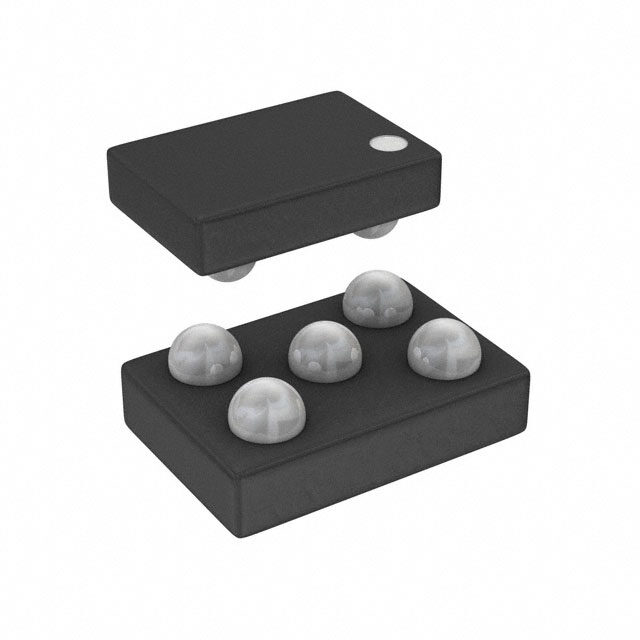
| 供应商器件封装 | 6-SON(2x2) |
| 其它名称 | 296-23105-6 |
| 包装 | Digi-Reel® |
| 单位重量 | 9.700 mg |
| 同步整流器 | 是 |
| 商标 | Texas Instruments |
| 安装类型 | 表面贴装 |
| 安装风格 | SMD/SMT |
| 封装 | Reel |
| 封装/外壳 | 6-WDFN 裸露焊盘 |
| 封装/箱体 | WSON-6 |
| 工作温度 | -40°C ~ 85°C |
| 工作温度范围 | - 40 C to + 85 C |
| 工厂包装数量 | 250 |
| 开关频率 | 2.25 MHz |
| 拓扑结构 | Buck |
| 最大输入电压 | 5.5 V |
| 最小工作温度 | - 40 C |
| 标准包装 | 1 |
| 电压-输入 | 2.5 V ~ 5.5 V |
| 电压-输出 | 0.85 V ~ 5.5 V |
| 电流-输出 | 600mA |
| 类型 | 降压(降压) |
| 系列 | TPS62560 |
| 输出数 | 1 |
| 输出电压 | Adj |
| 输出电流 | 600 mA |
| 输出端数量 | 1 Output |
| 输出类型 | 可调式 |
| 配用 | /product-detail/zh/TPS62560EVM-330/TPS62560EVM-330-ND/1908092 |
| 频率-开关 | 2.25MHz |


- 商务部:美国ITC正式对集成电路等产品启动337调查
- 曝三星4nm工艺存在良率问题 高通将骁龙8 Gen1或转产台积电
- 太阳诱电将投资9.5亿元在常州建新厂生产MLCC 预计2023年完工
- 英特尔发布欧洲新工厂建设计划 深化IDM 2.0 战略
- 台积电先进制程称霸业界 有大客户加持明年业绩稳了
- 达到5530亿美元!SIA预计今年全球半导体销售额将创下新高
- 英特尔拟将自动驾驶子公司Mobileye上市 估值或超500亿美元
- 三星加码芯片和SET,合并消费电子和移动部门,撤换高东真等 CEO
- 三星电子宣布重大人事变动 还合并消费电子和移动部门
- 海关总署:前11个月进口集成电路产品价值2.52万亿元 增长14.8%


PDF Datasheet 数据手册内容提取
Product Sample & Technical Tools & Support & Folder Buy Documents Software Community TPS62561 TPS62560,TPS62562 SLVS815D–JANUARY2008–REVISEDOCTOBER2016 TPS6256x 2.25-MHz, 600-mA Step-Down Converter in TSOT and 2 × 2 × 0.8-mm QFN Package 1 Features 3 Description • OutputCurrentupto600mA The TPS62560 device is a high efficiency 1 synchronous step down converter, optimized for • InputVoltageRangefrom2.5Vto5.5V battery powered portable applications. It provides up • OutputVoltageAccuracyinPWMMode±2.5% to 600-mA output current from batteries, such as • Typical15-μAQuiescentCurrent single Li-Ion or other common chemistry AA and AAA cells. • 100%DutyCycleforLowestDropout • SoftStart With an input voltage range of 2.5 V to 5.5 V, the device is targeted to power a large variety of portable • AvailableinaSmallSOT,and handheldequipmentorPOLapplications. 2mm×2mm× 0.8mmSONPackage The TPS62560 family operates at 2.25-MHz fixed • ForImprovedFeaturesSet,SeetheTPS62290 switching frequency and enters a Power Save Mode device(SLVS764) operation at light load currents to maintain a high efficiencyovertheentireloadcurrentrange. 2 Applications The Power Save Mode is optimized for low output • PDAs,PocketPCs,PortableMediaPlayers voltage ripple. For low noise applications, the device • Low-PowerDSPSupply can be forced into fixed frequency PWM mode by • Point-of-Load(POL)Applications pulling the MODE pin high. In the shutdown mode the current consumption is reduced to less than 1 µA. The TPS62560 allows the use of small inductors and capacitorstoachieveasmallsolutionsize. TPS62560 and TPS62562 are available in a 2-mm × 2-mm,6-pinSONpackage,whereastheTPS62561is availableina5-pinSOTpackage. DeviceInformation(1) PARTNUMBER PACKAGE BODYSIZE(NOM) TPS62560, SON(6) 2.00mm×2.00mm TPS62562 TPS62561 SOT(5) 2.90mm×1.60mm (1) For all available packages, see the orderable addendum at theendofthedatasheet. TypicalApplicationSchematic EfficiencyvsOutputCurrent VIN= 2.5 V to 5.5 V TPS62560DRV 2.2LmH Up to 600 mA 100 VIN SW VOUT CIN EN R1 C221 pF COUT 90 VIN= 2.7 V 4.7mF 10mF 80 V = 3 V GND FB IN V = 3.6 V R2 % 70 IN MODE – y 60 VIN= 4.5 V c Copyright © 2016,Texas Instruments Incorporated n e 50 ci Effi 40 – h 30 VOUT= 1.8 V MODE = GND 20 L= 2.2mH DCR 110 mR 10 0 0.01 0.1 1 10 100 1000 I –Output Current–mA OUT 1 An IMPORTANT NOTICE at the end of this data sheet addresses availability, warranty, changes, use in safety-critical applications, intellectualpropertymattersandotherimportantdisclaimers.PRODUCTIONDATA.
TPS62561 TPS62560,TPS62562 SLVS815D–JANUARY2008–REVISEDOCTOBER2016 www.ti.com Table of Contents 1 Features.................................................................. 1 9 ApplicationandImplementation........................ 11 2 Applications........................................................... 1 9.1 ApplicationInformation............................................11 3 Description............................................................. 1 9.2 TypicalApplication .................................................11 4 RevisionHistory..................................................... 2 9.3 SystemExamples ..................................................18 5 DeviceComparisonTable..................................... 4 10 PowerSupplyRecommendations..................... 18 6 PinConfigurationandFunctions......................... 4 11 Layout................................................................... 19 11.1 LayoutGuidelines.................................................19 7 Specifications......................................................... 5 11.2 LayoutExamples...................................................19 7.1 AbsoluteMaximumRatings......................................5 12 DeviceandDocumentationSupport................. 21 7.2 ESDRatings..............................................................5 7.3 RecommendedOperatingConditions.......................5 12.1 DeviceSupport ....................................................21 7.4 ThermalInformation..................................................5 12.2 RelatedLinks........................................................21 7.5 ElectricalCharacteristics...........................................6 12.3 ReceivingNotificationofDocumentationUpdates21 7.6 TypicalCharacteristics..............................................7 12.4 CommunityResources..........................................21 12.5 Trademarks...........................................................21 8 DetailedDescription.............................................. 8 12.6 ElectrostaticDischargeCaution............................21 8.1 Overview...................................................................8 12.7 Glossary................................................................21 8.2 FunctionalBlockDiagram.........................................8 13 Mechanical,Packaging,andOrderable 8.3 FeatureDescription...................................................9 Information........................................................... 22 8.4 DeviceFunctionalModes........................................10 4 Revision History NOTE:Pagenumbersforpreviousrevisionsmaydifferfrompagenumbersinthecurrentversion. ChangesfromRevisionC(December2009)toRevisionD Page • AddedESDRatingstable,FeatureDescriptionsection,DeviceFunctionalModes,ApplicationandImplementation section,PowerSupplyRecommendationssection,Layoutsection,DeviceandDocumentationSupportsection,and Mechanical,Packaging,andOrderableInformationsection.................................................................................................. 1 • RemovedOrderingInformationtable .................................................................................................................................... 1 • ChangedtextstringFrom".....upto1000-mAoutputcurrent.."To".....upto600-mAoutputcurrent.."inDescription.........1 • CorrectedtypographicalerrorsinFigure32;from"V =2Vto6V"to"V =2.5Vto5.5V"............................................. 18 IN IN ChangesfromRevisionB(March2009)toRevisionC Page • DeletedHighEfficiencyStepDownConverter....................................................................................................................... 1 • Deleted"Wide"fromFeaturesbullet...................................................................................................................................... 1 • Deleted"forLi-IonBatteriesWithExtendedVoltageRange"fromFeatures ........................................................................ 1 • Deleted"AdjustableandFixedOutput-VoltageOptions"fromFeatures................................................................................ 1 • Deleted"2.25MHzFixedFrequencyOperation"fromFeatures............................................................................................ 1 • Deleted"PowerSaveModeatLightLoadCurrents"fromFeatures ..................................................................................... 1 • Deleted"VoltagePositioningatLightLoads"fromFeatures.................................................................................................. 1 • Deleted"Allows<1-mmSolutionHeight"fromFeatures....................................................................................................... 1 • ChangedDescriptiontobetterreflectdevicecapabilitiesanddifferencestoTPS62260....................................................... 1 ChangesfromRevisionA(July2008)toRevisionB Page • AddedTPS62562devicenumber........................................................................................................................................... 1 2 SubmitDocumentationFeedback Copyright©2008–2016,TexasInstrumentsIncorporated ProductFolderLinks:TPS62561TPS62560 TPS62562
TPS62561 TPS62560,TPS62562 www.ti.com SLVS815D–JANUARY2008–REVISEDOCTOBER2016 ChangesfromOriginal(January2008)toRevisionA Page • Changedatalllevels.RevisionAisacompleterewriteofthisdatasheet............................................................................ 1 Copyright©2008–2016,TexasInstrumentsIncorporated SubmitDocumentationFeedback 3 ProductFolderLinks:TPS62561TPS62560 TPS62562
TPS62561 TPS62560,TPS62562 SLVS815D–JANUARY2008–REVISEDOCTOBER2016 www.ti.com 5 Device Comparison Table PartNumber Package ModePin OutputVoltage(1) DeviceMarking(2) TPS62560 SON(6) yes Adjustable CEY TPS62561 SOT(5) forcedPWMonly Adjustable CVO TPS62562 SON(6) yes 1.8Vfixed NXT (1) ContactTIforotherfixedoutputvoltageoptions (2) Forthemostcurrentpackageandorderinginformation,seeMechanical,Packaging,andOrderableInformation,orseetheTIwebsiteat www.ti.com 6 Pin Configuration and Functions DDCPackage 5-PinSOT DRVPackage TopView 6-PinSON TopView VIN 1 5 SW SW 1 6 GND Thermal MODE 2 5 V GND 2 Pad IN FB 3 4 EN EN 3 4 FB PinFunctions PIN No. No. I/O DESCRIPTION NAME QFN-6 TSOT23-5 Thisistheenablepinofthedevice.Pullingthispintolowforcesthedeviceinto EN 4 3 I shutdownmode.Pullingthispintohighenablesthedevice.Thispinmustbeterminated. Feedbackpinfortheinternalregulationloop.Connecttheexternalresistordividertothis FB 3 4 I pin.Inthefixed-output-voltageoption,connectthisterminaldirectlytotheoutput capacitor. GND 6 2 — GNDsupplypin ThispinisonlyavailableasaQFNpackageoption.MODEpin=highforcesthedevice MODE 2 N/A I tooperateinthefixed-frequencyPWMmode.MODEpin=lowenablesthepower-save modewithautomatictransitionfromPFMmodetofixed-frequencyPWMmode. ThisistheswitchpinandisconnectedtotheinternalMOSFETswitches.Connectthe SW 1 5 O externalinductorbetweenthispinandtheoutputcapacitor. V 5 1 — V power-supplypin IN IN Exposed Mustbesolderedtoachieveappropriatepowerdissipation.Shouldbeconnectedto Thermal — N/A — GND. Pad 4 SubmitDocumentationFeedback Copyright©2008–2016,TexasInstrumentsIncorporated ProductFolderLinks:TPS62561TPS62560 TPS62562
TPS62561 TPS62560,TPS62562 www.ti.com SLVS815D–JANUARY2008–REVISEDOCTOBER2016 7 Specifications 7.1 Absolute Maximum Ratings overoperatingfree-airtemperaturerange(unlessotherwisenoted)(1) MIN MAX UNIT Inputvoltagerange(2) –0.3 7 VoltagerangeatEN,MODE –0.3 V +0.3,≤7 V IN VoltageonSW –0.3 7 Peakoutputcurrent Internallylimited A T Maximumoperatingjunctiontemperature –40 125 °C J T Storagetemperature –65 150 °C stg (1) Stressesbeyondthoselistedunderabsolutemaximumratingsmaycausepermanentdamagetothedevice.Thesearestressratings onlyandfunctionaloperationofthedeviceattheseoranyotherconditionsbeyondthoseindicatedunderrecommendedoperating conditionsisnotimplied.Exposuretoabsolute-maximum-ratedconditionsforextendedperiodsmayaffectdevicereliability. (2) Allvoltagevaluesarewithrespecttothenetworkgroundterminal. 7.2 ESD Ratings VALUE UNIT Human-bodymodel(HBM),perANSI/ESDA/JEDECJS-001(2) ±2000 V(ESD) Electrostaticdischarge(1) CCh1a0r1g(e3)d-devicemodel(CDM),perJEDECspecificationJESD22- ±1000 V Machinemodel ±200 (1) Thehuman-bodymodelisa100-pFcapacitordischargedthrougha1.5-kΩresistorintoeachterminal.Themachinemodelisa200-pF capacitordischargeddirectlyintoeachterminal. (2) JEDECdocumentJEP155statesthat500-VHBMallowssafemanufacturingwithastandardESDcontrolprocess.Manufacturingwith lessthan500-VHBMispossiblewiththenecessaryprecautions. (3) JEDECdocumentJEP157statesthat250-VCDMallowssafemanufacturingwithastandardESDcontrolprocess.Manufacturingwith lessthan250-VCDMispossiblewiththenecessaryprecautions. 7.3 Recommended Operating Conditions MIN MAX UNIT V Supplyvoltage 2.5 5.5 V IN V Outputvoltagerangeforadjustablevoltage 0.85 V V OUT IN T Operatingambienttemperature –40 85 °C A T Operatingjunctiontemperature –40 125 °C J 7.4 Thermal Information TPS62560, TPS62561 TPS62562 THERMALMETRIC(1) UNIT DRV(SON) DDC(SOT) 6PINS 5PINS R Junction-to-ambientthermalresistance 67.8 226.9 °C/W θJA R Junction-to-case(top)thermalresistance 88.5 40.7 °C/W θJC(top) R Junction-to-boardthermalresistance 37.2 48.8 °C/W θJB ψ Junction-to-topcharacterizationparameter 2.0 0.5 °C/W JT ψ Junction-to-boardcharacterizationparameter 37.6 48.1 °C/W JB R Junction-to-case(bottom)thermalresistance 7.9 n/a °C/W θJC(bot) (1) Formoreinformationabouttraditionalandnewthermalmetrics,seetheSemiconductorandICPackageThermalMetricsapplication report,SPRA953. Copyright©2008–2016,TexasInstrumentsIncorporated SubmitDocumentationFeedback 5 ProductFolderLinks:TPS62561TPS62560 TPS62562
TPS62561 TPS62560,TPS62562 SLVS815D–JANUARY2008–REVISEDOCTOBER2016 www.ti.com 7.5 Electrical Characteristics Overfulloperatingambienttemperaturerange,typicalvaluesareatT =25°C.Unlessotherwisenoted,specificationsapply A forconditionV =EN=3.6V.ExternalcomponentsC =4.7μF0603,C =10μF0603,L=2.2μH IN IN OUT PARAMETER TESTCONDITIONS MIN TYP MAX UNIT SUPPLY VIN Inputvoltagerange 2.5 5.5 V IOUT Outputcurrent VIN2.5Vto5.5V 600 mA IOUT=0mA,PFMmodeenabled 15 (MODE=GND),devicenotswitching IOUT=0mA,PFMmodeenabled μA IQ Operatingquiescentcurrent ((1M)ODE=GND),deviceswitching,VOUT=1.8V,See 18.5 IOUT=0mA,switchingwithnoload (MODE=VIN),PWMoperation,VOUT=1.8V, 3.8 mA VIN=3V ISD Shutdowncurrent EN=GND 0.5 μA Falling 1.85 UVLO Undervoltagelockoutthreshold V Rising 1.95 ENABLE,MODE VIH High-levelinputvoltage,EN,MODE 2V≤VIN≤5.5V 1 VIN V VIL Low-levelinputvoltage,EN,MODE 2V≤VIN≤5.5V 0 0.4 V IIN Inputbiascurrent,EN,MODE EN,MODE=GNDorVIN 0.01 1 μA POWERSWITCH HighsideMOSFETon-resistance 252 492 RDS(on) VIN=VGS=3.6V,TA=25°C mΩ LowsideMOSFETon-resistance 194 391 Forwardcurrentlimit,highandlowside ILIMF MOSFET VIN=VGS=3.6V 0.8 1 1.2 A Thermalshutdown Increasingjunctiontemperature 140 TSD °C Thermal-shutdownhysteresis Decreasingjunctiontemperature 20 OSCILLATOR fSW Oscillatorfrequency 2V≤VIN≤5.5V 2.25 MHz OUTPUT VOUT Adjustable-outputvoltagerange 0.85 VIN V VOUT TPS62562fixedoutputvoltage VIN≥1.8V 1.8 V Vref Referencevoltage 600 mV MODE=VIN,PWMoperation,forfixed-output- Feedbackvoltage,PWMmode voltageversionsVFB=VOUT, –2.5% 0% 2.5% 2.5V≤VIN ≤5.5V,0mA≤IOUT≤600mA(2) VFB MODE=GND,deviceinPFMmode,voltage Feedbackvoltage,PFMmode positioningactive(1) 1% Loadregulation PWMmode –1 %/A tStartUp Start-uptime TimefromactiveENtoreach95%ofVOUTnominal 500 μs tRamp VOUTramp-uptime Timetorampfrom5%to95%ofVOUT 250 μs Ilkg LeakagecurrentintoSWterminal VIN=3.6V,VIN=VOUT=VSW,EN=GND(3) 0.5 1 μA (1) InPFMmode,theinternalreferencevoltageissettotyp.1.01×V .Seethesection. ref (2) ForV =V +0.6V IN OUT (3) Infixed-output-voltageversions,theinternalresistordividernetworkisdisconnectedfromtheFBterminal. 6 SubmitDocumentationFeedback Copyright©2008–2016,TexasInstrumentsIncorporated ProductFolderLinks:TPS62561TPS62560 TPS62562
TPS62561 TPS62560,TPS62562 www.ti.com SLVS815D–JANUARY2008–REVISEDOCTOBER2016 7.6 Typical Characteristics 0.8 20 EN = GND MMOODDEE == GGNNDD, EENN == VVIN, 0.7 IN Am 18 DDeevviiccee NNoott SSwwiittcchhiinngg TTAA== 8855°oCC − N 0.6 A ent Into VI 0.5 TA = 85oC Current–m 16 TTAA== 2255o°CC urr 0.4 nt 14 C e wn 0.3 esc - ShutdoD 0.2 TA = 25oC TA = -40oC I–QuiQ 1102 TTAA== –-4400o°CC IS 0.1 0 8 2.5 3 3.5 4 4.5 5 5.5 8222 22..55 33 33..55 44 44..55 55 55..55 66 V −Input Voltage−V VV –−InInppuutt V Vooltltaaggee–−VV IN IINN Figure1.ShutdownCurrentintoVINvsInputVoltage Figure2.QuiescentCurrentvsInputVoltage W 0.8 W 0.4 − High-Side Switching − Low-Side Switching nce 0.7 nce0.35 State Resista 00..56 TA = 85oC State Resista0.02.53 TA = 85oC On- TA = 25oC On- TA = 25oC urce 0.4 urce 0.2 So 0.3 So0.15 n- n- Drai 0.2 Drai 0.1 Static 0.1 TA =−40oC Static 0.05 TA =–40oC − − RDS(on) 02 2.5 3 3.5 4 4.5 5 RDS(on) 02 2.5 3 3.5 4 4.5 5 VIN−Input Voltage−V VIN−Input Voltage−V G012 Figure4.StaticDrain-SourceON-StateResistancevsInput Figure3.StaticDrain-SourceON-StateResistance Voltage Copyright©2008–2016,TexasInstrumentsIncorporated SubmitDocumentationFeedback 7 ProductFolderLinks:TPS62561TPS62560 TPS62562
TPS62561 TPS62560,TPS62562 SLVS815D–JANUARY2008–REVISEDOCTOBER2016 www.ti.com 8 Detailed Description 8.1 Overview The TPS62560/62 step-down converters operate with typically 2.25-MHz fixed-frequency pulse-width modulation (PWM) at moderate to heavy load currents. At light load currents, the converter can automatically enter power- save mode, and then operates in PFM mode. However, the TPS62561 operates with fixed-frequency PWM only, alsoatlightloadconditions. During PWM operation, the converter uses a unique fast-response voltage-mode control scheme with input- voltage feed-forward to achieve good line and load regulation, allowing the use of small ceramic input and output capacitors. At the beginning of each clock cycle initiated by the clock signal, the high-side MOSFET switch is turned on. The current flows from the input capacitor via the high-side MOSFET switch through the inductor to the output capacitor and load. During this phase, the current ramps up until the PWM comparator trips and the control logic turns off the switch. The current-limit comparator also turns off the switch in case the current limit of thehigh-sideMOSFETswitchisexceeded.Afteradeadtime,whichpreventsshoot-throughcurrent,thelow-side MOSFET rectifier is turned on and the inductor current ramps down. The current flows from the inductor to the outputcapacitorandtotheload.Itreturnsbacktotheinductorthroughthelow-sideMOSFETrectifier. The next cycle is initiated by the clock signal again turning off the low-side MOSFET rectifier and turning on the onthehigh-sideMOSFETswitch. 8.2 Functional Block Diagram V IN Current- Limit Comparator V Thermal Undervoltage IN Shutdown Lockout1.8V Limit EN High Side PFM Comparator Reference +1%Voltage positioning 0.6V VREF FB VREF+1% Only in 2x2SON Gate Driver MODE MODE Control ShootA-Tnhtir-ough ErrorAmplifier Stage Softstart SW1 VOUTRAMP VREF CONTROL Integrator FB FB PWM Zero-Pole Comp. Amp. Limit RI1 GND Low Side RI..N RI3 Sawtooth 2.25-MHz CLiumrrite Cnto-mparator Generator Oscillator Int.Resistor Network GND Copyright © 2016,Texas Instruments Incorporated 8 SubmitDocumentationFeedback Copyright©2008–2016,TexasInstrumentsIncorporated ProductFolderLinks:TPS62561TPS62560 TPS62562
TPS62561 TPS62560,TPS62562 www.ti.com SLVS815D–JANUARY2008–REVISEDOCTOBER2016 8.3 Feature Description 8.3.1 DynamicVoltagePositioning This feature reduces the voltage under/overshoots at load steps from light to heavy load and vice versa. It is active in power-save mode and regulates the output voltage 1% higher than the nominal value. This provides moreheadroomforboththevoltagedropataloadstep,andthevoltageincreaseataloadthrow-off. Output voltage Vout +1% Voltage Positioning PFM Comparator threshold Light load PFM Mode Vout (PWM) moderate to heavy load PWM Mode Figure5. PowerSaveModeOperationWithAutomaticModeTransition 8.3.2 UndervoltageLockout The undervoltage lockout circuit prevents the device from malfunctioning at low input voltages and from excessive discharge of the battery and disables the output stage of the converter. The undervoltage lockout thresholdistypically1.85VwithfallingV . IN 8.3.3 ModeSelection TheMODEterminalallowsmodeselectionbetweenforced-PWMmodeandpower-savemode. Connecting this terminal to GND enables the power-save mode with automatic transition between PWM and PFMmodes.PullingtheMODEterminalhighforcestheconvertertooperateinfixed-frequencyPWMmodeeven at light load currents. This allows simple filtering of the switching frequency for noise-sensitive applications. In thismode,theefficiencyislowercomparedtothepower-savemodeduringlightloads. The state of the MODE terminal can be changed during operation to allow efficient power management by adjustingtheoperationmodeoftheconvertertothespecificsystemrequirements. 8.3.4 Enable The device is enabled by setting the EN terminal to high. During the start-up time t , the internal circuits are Start Up settled and the soft-start circuit is activated. The EN input can be used to control power sequencing in a system with various dc/dc converters. The EN terminal can be connected to the output of another converter, to drive the EN terminal high to achieve a sequencing of the given supply rails. With EN = GND, the device enters shutdown mode, in which all internal circuits are disabled. In fixed-output-voltage versions, the internal resistor divider networkisthendisconnectedfromtheFBterminal. 8.3.5 ThermalShutdown As soon as the junction temperature, T , exceeds 140°C (typical), the device goes into thermal shutdown. In this J mode, the high-side and low-side MOSFETs are turned off. The device continues its operation when the junction temperaturefallsbelowthethermalshutdownhysteresis. Copyright©2008–2016,TexasInstrumentsIncorporated SubmitDocumentationFeedback 9 ProductFolderLinks:TPS62561TPS62560 TPS62562
TPS62561 TPS62560,TPS62562 SLVS815D–JANUARY2008–REVISEDOCTOBER2016 www.ti.com 8.4 Device Functional Modes 8.4.1 Soft-Start The TPS62560 has an internal soft-start circuit that controls the ramp-up of the output voltage. The output voltage ramps up from 5% to 95% of its nominal value typically within 250 μs. This limits the inrush current into theconverterduringramp-upandpreventspossibleinputvoltagedropswhenabatteryorhigh-impedancepower sourceisused.Thesoft-startcircuitisenabledwithinthestart-uptimet . StartUp 8.4.2 Power-SaveMode The power-save mode is enabled with the MODE terminal set to the low level. If the load current decreases, the converter enters the power-save mode of operation automatically. During power-save mode, the converter skips switching and operates with reduced frequency in PFM mode with a minimum quiescent current to maintain high efficiency. The converter positions the output voltage typically 1% above the nominal output voltage. This voltage positioningfeatureminimizesvoltagedropscausedbyasuddenloadstep. The transition from PWM mode to PFM mode occurs once the inductor current in the low-side MOSFET switch becomeszero,whichindicatesdiscontinuousconductionmode. During the power-save mode, the output voltage is monitored with a PFM comparator. As the output voltage falls below the PFM comparator threshold of V nominal + 1%, the device starts a PFM current pulse. The high- OUT side MOSFET switch turns on, and the inductor current ramps up. After the on-time expires, the switch is turned offandthelow-sideMOSFETswitchisturnedonuntiltheinductorcurrentbecomeszero. The converter effectively delivers a current to the output capacitor and the load. If the load is below the delivered current, the output voltage rises. If the output voltage is equal to or higher than the PFM comparator threshold, thedevicestopsswitchingandentersasleepmodewithtypical15-μAcurrentconsumption. If the output voltage is still below the PFM comparator threshold, a sequence of further PFM current pulses is generated until the PFM comparator threshold is reached. The converter starts switching again once the output voltagedropsbelowthePFMcomparatorthreshold. With a fast single-threshold comparator, the output-voltage ripple during PFM-mode operation can be kept small. The PFM pulse is time controlled, which allows modifying the charge transferred to the output capacitor by the valueoftheinductor.TheresultingPFMoutput-voltagerippleandPFMfrequencydependprimarilyonthesizeof theoutputcapacitorandtheinductorvalue.Increasingoutputcapacitorvaluesandinductorvaluesminimizesthe outputripple.ThePFMfrequencydecreaseswithsmallerinductorvaluesandincreaseswithlargervalues. The PFM mode is left and PWM mode entered in case the output current can no longer be supported in PFM mode.Thepower-savemodecanbedisabledbysettingtheMODEterminaltohigh.Theconverterthenoperates inthefixed-frequencyPWMmode. 8.4.2.1 100%Duty-CycleLow-DropoutOperation The device starts to enter 100% duty-cycle mode once the input voltage comes close to the nominal output voltage.Inordertomaintaintheoutputvoltage,thehigh-sideMOSFETswitchisturnedon100%foroneormore cycles. With further decreasing V , the high-side MOSFET switch is turned on completely. In this case, the converter IN offers a low input-to-output voltage difference. This is particularly useful in battery-powered applications to achievelongestoperationtimebytakingfulladvantageofthewholebattery-voltagerange. The minimum input voltage to maintain regulation depends on the load current and output voltage; and, can be calculatedas: sp V min=V max+I max×(R max+R ) IN OUT OUT DS(on) L where • I max=maximumoutputcurrentplusinductorripplecurrent OUT • R max=maximumP-channelswitchR DS(on) DS(on) • R =dcresistanceoftheinductor L • V max=nominaloutputvoltageplusmaximumoutputvoltagetolerance (1) OUT 10 SubmitDocumentationFeedback Copyright©2008–2016,TexasInstrumentsIncorporated ProductFolderLinks:TPS62561TPS62560 TPS62562
TPS62561 TPS62560,TPS62562 www.ti.com SLVS815D–JANUARY2008–REVISEDOCTOBER2016 Device Functional Modes (continued) 8.4.2.2 Short-CircuitProtection The high-side and low-side MOSFET switches are short-circuit protected with maximum switch current = I . LIMF The current in the switches is monitored by current-limit comparators. Once the current in the high-side MOSFET switch exceeds the threshold of its current-limit comparator, it turns off and the low-side MOSFET switch is activated to ramp down the current in the inductor and high-side MOSFET switch. The high-side MOSFET switch can only turn on again after the current in the low-side MOSFET switch has decreased below the threshold of its current-limitcomparator. 9 Application and Implementation NOTE Information in the following applications sections is not part of the TI component specification, and TI does not warrant its accuracy or completeness. TI’s customers are responsible for determining suitability of components for their purposes. Customers should validateandtesttheirdesignimplementationtoconfirmsystemfunctionality. 9.1 Application Information TheTPS6256xdevicesarehigh-efficiencysynchronousstep-downDC–DCconverterfeaturingpower-savemode or2.25-MHzfixedfrequencyoperation. 9.2 Typical Application VIN= 2.5 V to 5.5 V TPS62560DRV 2.2LmH Up to 600 mA VIN SW VOUT C CIN EN R1 221 pF COUT 4.7mF 10mF GND FB R 2 MODE Copyright © 2016,Texas Instruments Incorporated Figure6. TPS62560DRVAdjustable 9.2.1 DesignRequirements The TPS6256x is a highly integrated DC/DC converter. The output voltage is set with an external voltage divider for the adjustable output voltage version. The output voltage is fixed to 1.8V for the TPS62562. For proper operation a input- and output capacitor and an inductor is required. Table 2 shows the components used for the applicationcharacteristiccurves. 9.2.2 DetailedDesignProcedure 9.2.2.1 OutputVoltageSetting For adjustable output voltage versions, the output voltage can be calculated by Equation 2 with the internal referencevoltageV =0.6Vtypically. REF æ R ö VOUT =VREF´ç1+R1 ÷ è 2 ø (2) To minimize the current through the feedback divider network, R should be 180 kΩ or 360 kΩ. The sum of R 2 1 and R should not exceed ~1 MΩ, to keep the network robust against noise. An external feed-forward capacitor 2 C is required for optimum load transient response. The value of C should be in the range between 22 pF and 1 1 33pF. Incaseofusingthefixedoutputvoltageversion(TPS62562),V hastobeconnectedtothefeedbackpinFB. out Copyright©2008–2016,TexasInstrumentsIncorporated SubmitDocumentationFeedback 11 ProductFolderLinks:TPS62561TPS62560 TPS62562
TPS62561 TPS62560,TPS62562 SLVS815D–JANUARY2008–REVISEDOCTOBER2016 www.ti.com Typical Application (continued) RoutetheFBlineawayfromnoisesources,suchastheinductorortheSWline. 9.2.2.2 OutputFilterDesign(inductorandOutputCapacitor) The TPS62560 is designed to operate with inductors in the range of 1.5 μH to 4.7 μH and with output capacitors in the range of 4.7 μF to 22 μF. The part is optimized for operation with a 2.2-μH inductor and 10-μF output capacitor. Larger or smaller inductor values can be used to optimize the performance of the device for specific operation conditions. For stable operation, the L and C values of the output filter may not fall below 1 μH effective inductanceand3.5μFeffectivecapacitance. 9.2.2.2.1 InductorSelection The inductor value has a direct effect on the ripple current. The selected inductor must be rated for its dc resistance and saturation current. The inductor ripple current (ΔI ) decreases with higher inductance and L increaseswithhigherV orV . IN OUT The inductor selection also impacts the output voltage ripple in PFM mode. Higher inductor values lead to lower output voltage ripple and higher PFM frequency; lower inductor values lead to a higher output voltage ripple but lowerPFMfrequency. Equation 3 calculates the maximum inductor current in PWM mode under static load conditions. The saturation current of the inductor should be rated higher than the maximum inductor current as calculated with Equation 4. This is recommended because during heavy load transients the inductor current rises above the calculated value. V 1(cid:2) OUT V (cid:1)I (cid:3)V (cid:1) IN L OUT L(cid:1)f (3) (cid:1)I I max(cid:2)I max(cid:1) L L out 2 where • f=Switchingfrequency(2.25MHz,typical) • L=Inductorvalue • ΔI =Peak-to-peakinductorripplecurrent L • I max=Maximuminductorcurrent (4) L A more conservative approach is to select the inductor current rating just for the switch current limit I of the LIMF converter. Accepting larger values of ripple current allows the use of lower inductance values, but results in higher output voltageripple,greatercorelosses,andloweroutputcurrentcapability. The total losses of the coil have a strong impact on the efficiency of the dc/dc conversion and consist of both the lossesinthedcresistance(R )andthefollowingfrequency-dependentcomponents: (DC) • Thelossesinthecorematerial(magnetichysteresisloss,especiallyathighswitchingfrequencies) • Additionallossesintheconductorfromtheskineffect(currentdisplacementathighfrequencies) • Magneticfieldlossesoftheneighboringwindings(proximityeffect) • Radiationlosses 12 SubmitDocumentationFeedback Copyright©2008–2016,TexasInstrumentsIncorporated ProductFolderLinks:TPS62561TPS62560 TPS62562
TPS62561 TPS62560,TPS62562 www.ti.com SLVS815D–JANUARY2008–REVISEDOCTOBER2016 Table1.ListofInductors DIMENSIONS,mm INDUCTANCE,μH INDUCTORTYPE SUPPLIER(1) 2,5×2×1max 2 MIPS2520D2R2 FDK 2,5×2×1,2max 2 MIPSA2520D2R2 FDK 2,5×2×1max 2.2 KSLI-252010AG2R2 HitachiMetals 2,5×2×1,2max 2.2 LQM2HPN2R2MJ0L Murata 3×3×1,5max 2.2 LPS30152R2 Coilcraft (1) SeeThird-PartyProductsDisclaimer 9.2.2.2.2 OutputCapacitorSelection The advanced fast-response voltage-mode control scheme of the TPS62560 allows the use of tiny ceramic capacitors. Ceramic capacitors with low ESR values have the lowest output voltage ripple and are recommended. The output capacitor requires either an X7R or X5R dielectric. Y5V and Z5U dielectric capacitors, asidefromtheirwidevariationincapacitanceovertemperature,becomeresistiveathighfrequencies. At nominal load current, the device operates in PWM mode, and the RMS ripple current is calculated by Equation5: V 1- OUT V 1 I = V ´ IN ´ RMSCOUT OUT L´f 2 3 (5) At nominal load current, the device operates in PWM mode, and the overall output voltage ripple is the sum of thevoltagespikecausedbytheoutputcapacitorESRplusthevoltageripplecausedbycharginganddischarging theoutputcapacitorshowninEquation6: V 1- OUT V æ 1 ö DVOUT = VOUT´ L´fIN ´ç8´C ´f +ESR÷ è OUT ø (6) At light load currents, the converter operates in power-save mode, and the output voltage ripple is dependent on the output capacitor and inductor values. Larger output capacitor and inductor values minimize the voltage ripple inPFMmodeandtightendcoutputaccuracyinPFMmode. 9.2.2.2.3 InputCapacitorSelection An input capacitor is required for best input voltage filtering and minimizing the interference with other circuits caused by high input voltage spikes. For most applications, a 4.7-μF to 10-μF ceramic capacitor is recommended. Because a ceramic capacitor loses up to 80% of its initial capacitance at 5 V, it is recommended that 10-μF input capacitors be used for input voltages > 4.5 V. The input capacitor can be increased without any limit for better input voltage filtering. Take care when using only small ceramic input capacitors. When a ceramic capacitor is used at the input and the power is being supplied through long wires, such as from a wall adapter, a load step at the output or V step on the input can induce ringing at the V terminal. This ringing can couple to IN IN theoutputandbemistakenasloopinstabilityorcouldevendamagethepartbyexceedingthemaximumratings. Table2.ListofCapacitors(1) CAPACITANCE TYPE SIZE SUPPLIER 4.7μF GRM188R60J475K 0603—1,6×0,8×0,8mm Murata 10μF GRM188R60J106M69D 0603—1,6×0,8×0,8mm Murata (1) SeeThird-PartyProductsDisclaimer Copyright©2008–2016,TexasInstrumentsIncorporated SubmitDocumentationFeedback 13 ProductFolderLinks:TPS62561TPS62560 TPS62562
TPS62561 TPS62560,TPS62562 SLVS815D–JANUARY2008–REVISEDOCTOBER2016 www.ti.com 9.2.3 ApplicationCurves 100 100 90 90 V = 2.7 V IN 80 V = 3 V 80 IN V = 2.7 V IN 70 VIN= 3.6 V 70 % % V = 3 V y– 60 VIN= 4.5 V y– 60 IN VIN= 3.6 V c c cien 50 cien 50 VIN= 4.5 V Effi 40 Effi 40 – – h h 30 30 V = 1.8 V OUT 20 MODE = GND 20 VOUT= 1.8 V L= 2.2mH MODE = VIN 10 DCR 110 mR 10 L= 2.2mH 0 0 0.01 0.1 1 10 100 1000 1 10 100 1000 IOUT–Output Current–mA IOUT–Output Current–mA G002 G003 Figure7.EfficiencyvsOutputCurrent Figure8.EfficiencyvsOutputCurrent 100 100 V = 4.2 V IN 90 VIN= 4.2 V 90 V = 3.6 V IN 80 VIN= 3.6 V 80 VIN= 5 V % 70 VIN= 5 V % 70 VIN= 4.5 V – 60 V = 4.5 V – 60 y IN y c c n n cie 50 cie 50 Effi 40 Effi 40 – – h 30 VOUT= 3.3 V h 30 VOUT= 3.3 V MODE = VIN MODE = GND 20 L= 2.2mH 20 L= 2.2mH DCR 110 mW DCR = 110 mH 10 COUT= 10mF 0603 10 COUT= 10mF 0603 0 0 1 10 100 1000 0.01 0.1 1 10 100 1000 I –Output Current–mA OUT I –Output Current–mA OUT Figure9.EfficiencyvsOutputCurrent Figure10.EfficiencyvsOutputCurrent 100 100 90 90 V = 2.7 V IN 80 80 V = 4.5 V IN 70 70 % % V = 3.6 V − 60 − 60 IN ncy VIN = 4.5 V ncy Efficie 4500 VIN = 3.6 V Efficie 4500 VIN= 2.7 V − − h 30 VMOOUDTE= =1 .V2 INV h 30 VMOOUDTE= =1 .G2 NVD 20 L= 2mH 20 L= 2mH MIPSA2520 MIPSA2520 10 COUT= 10mF 0603 10 COUT= 10mF 0603 0 0 1 10 100 1000 0.01 0.1 1 10 100 1000 I −Output Current−mA I −Output Current−mA OUT OUT G004 G005 Figure11.EfficiencyvsOutputCurrent Figure12.EfficiencyvsOutputCurrent 14 SubmitDocumentationFeedback Copyright©2008–2016,TexasInstrumentsIncorporated ProductFolderLinks:TPS62561TPS62560 TPS62562
TPS62561 TPS62560,TPS62562 www.ti.com SLVS815D–JANUARY2008–REVISEDOCTOBER2016 V 3.6V IN V = 3.6 V V 1.8V, I 150mA IN VOUT10 mV/Div LO2U.2TmH, COUOTUT10mF 0603 M2VO/DDiEv VIOOUUTT== 1 10. 8m VA SW 2 V/Div SW 2V/Div PFM Mode Forced PWM Mode I 200 mA/Div COIL I coil 200mA/Div Time Base - 10ms/Div Time Base - 1ms/Div Figure13.TypicalOperation-PWMMode Figure14.ModePinTransitionfromPFMtoFORCEDPWM ModeatLightLoad M2 OV/DDEiv VIN= 3.6 V EN 2 V/Div VIN= 3.6 V VOUT= 1.8 V RLoad= 10Ω IOUT= 10 mA VOUT= 1.8 V I into C IN IN SW MODE = GND 2 V/Div SW 2 V/Div Forced PWM Mode PFM Mode V 2 V/Div OUT I COIL 200 mA/Div I 100 mA/Div IN Time Base - 2.5ms/Div Time Base - 100ms/Div Figure15.ModePinTransitionfromPWMtoPFMMODEat Figure16.Start-UPTiming LightLoad VIN3.6 V VIN3.6 V VOUT1.5 V VOUT50 mV/Div VOUT1.5 V VOUT50 mV/Div IOUT50 mAto 200 mA IOUT200 mAto 400 mA MODE =V IN IOUT200 mA/Div 400 mA I 200 mA/Div 200 mA OUT I 500 mA/Div COIL I 500 mA/Div COIL Time Base - 20ms/Div Time Base - 20ms/Div Figure17.ForcedPWMLoadTransient Figure18.ForcedPWMLoadTransient Copyright©2008–2016,TexasInstrumentsIncorporated SubmitDocumentationFeedback 15 ProductFolderLinks:TPS62561TPS62560 TPS62562
TPS62561 TPS62560,TPS62562 SLVS815D–JANUARY2008–REVISEDOCTOBER2016 www.ti.com SW 2 V/Div SW 2 V/Div V 3.6 V IN V 1.5 V V 3.6 V OUT VOUT50mV/Div VIONUT1.5 V IMOOUTDE15 =0 GmANDto 400 mA IMOOUTD1E5 =0 GmANDto 400 mA VOUT50 mV/Div I 500 mA/Div 400 mA 400 mA OUT I 500 mA/Div OUT 150mA 150mA ICOILl500mA/Div ICOIL500 mA/Div Time Base–500ms/Div Time Base–500ms/Div Figure19.PFMLoadTransient Figure20.PFMLoadTransient SW 2 V/Div SW 2 V/Div VIN3.6 V VIN3.6 V VOUT1.5 V VOUT1.5 V IMOOUTDE1 .=5 GmNADto 50 mA VOUT50 mV/Div IMOOUTD5E0 = m GANtoD1.5mA V 50mV/Div OUT 50 mA 50 mA IOUT50 mA/Div IOUT50 mA/Div 1.5 mA 1.5 mA ICOIL500 mA/Div ICOIL500 mA/Div Time Base–50ms/Div Time Base–50ms/Div Figure21.PFMLoadTransient Figure22.PFMLoadTransient SW 2 V/Div SW 2 V/Div VOUT50 mV/Div VIN3.6 V VIN3.6 V VOUT50 mV/Div VIOUT510.5m VAto 400 mA V 1.8 V OUT OUT MODE = GND I 50mAto 250 mA OUT MODE = GND 250 mA PFM Mode PWM Mode 400 mA IOUT200 mA/Div IOUT500 mA/Div 50 mA 50 mA ICOIL 500 mA/Div ICOIL 500mA/Div Time Base–20ms/Div Time Base–20ms/Div Figure23.PFMLoadTransient Figure24.PFMLoadTransient 16 SubmitDocumentationFeedback Copyright©2008–2016,TexasInstrumentsIncorporated ProductFolderLinks:TPS62561TPS62560 TPS62562
TPS62561 TPS62560,TPS62562 www.ti.com SLVS815D–JANUARY2008–REVISEDOCTOBER2016 SW 2 V/Div V 3.6V to 4.2V IN 500 mV/Div V 3.6 V IN V 1.5 V V 50 mV/Div OUT OUT I 50mAto 400 mA OUT MODE = GND PFM Mode PWM Mode I 500 mA/Div 400 mA OUT V = 1.8 V OUT 50 mA 50 mV/Div I = 50 mA OUT MODE = GND I 500 mA/Div COIL Time Base–20ms/Div Time Base–100ms/Div Figure25.PFMLoadTransient Figure26.PFMLineTransient VIN3.6V to 4.2V VOUT20 mV/Div 500 mV/Div SW 2 V/Div V = 1.8 V OUT 50 mV/Div I = 250 mA OUT MODE = GND I 200 mA/Div COIL Time Base–100ms/Div Time Base–10ms/Div Figure27.PWMLineTransient Figure28.TypicalOperation-PFMMode V 3.6 V; V 1.8 V, I 10mA, IN OUT OUT VOUT20 mV/Div ML=O D4.E7 =m HG, NCDOUT= 10mF 0603, SW 2 V/Div I 200 mA/Div COIL Time Base–2ms/Div Figure29.TypicalOperation-PFMMode Copyright©2008–2016,TexasInstrumentsIncorporated SubmitDocumentationFeedback 17 ProductFolderLinks:TPS62561TPS62560 TPS62562
TPS62561 TPS62560,TPS62562 SLVS815D–JANUARY2008–REVISEDOCTOBER2016 www.ti.com 9.3 System Examples TPS62560DRV L1 VIN= 2.5 V to 5.5 V 2.2mH VOUT= 1.2 V VIN SW R C C 1 1 C IN EN 360 kW 22 pF OUT 4.7mF 10mF FB GND R 2 360 kW MODE S0364_01 Copyright © 2016,Texas Instruments Incorporated Figure30. TPS62560Adjustable1.2-VOutput TPS62560DRV L1 VOUT= 1.5 V V = 2.5 V to 5.5 V 2.2mH Up to 600 mA IN VIN SW R C C 1 1 C IN EN 540 kW 22 pF OUT 4.7mF 10mF FB GND R 2 360 kW MODE S0365-01 Copyright © 2016,Texas Instruments Incorporated Figure31. TPS62560Adjustable1.5-VOutput TPS62562DRV L1 VOUT= 1.8 V V = 2.5 V to 5.5 V 2.2mH Up to 600 mA IN VIN SW C C IN EN OUT 4.7mF 10mF FB GND MODE S0366-01 Copyright © 2016,Texas Instruments Incorporated Figure32. TPS62562Fixed1.8-VOutput 10 Power Supply Recommendations The TPS6226x device has no special requirements for its input power supply. The input power supply output currentmustberatedaccordingtothesupplyvoltage,outputvoltage,andoutputcurrentoftheTPS6226x. 18 SubmitDocumentationFeedback Copyright©2008–2016,TexasInstrumentsIncorporated ProductFolderLinks:TPS62561TPS62560 TPS62562
TPS62561 TPS62560,TPS62562 www.ti.com SLVS815D–JANUARY2008–REVISEDOCTOBER2016 11 Layout 11.1 Layout Guidelines As for all switching power supplies, the layout is an important step in the design. Proper function of the device demands careful attention to PCB layout. Take care in board layout to get the specified performance. If the layout is not carefully done, the regulator could show poor line and/or load regulation, stability issues as well as EMI problems. It is critical to provide a low inductance, impedance ground path. Therefore, use wide and short traces for the main current paths. The input capacitor should be placed as close as possible to the IC pins as wellastheinductorandoutputcapacitor. Connect the GND pin of the device to the exposed thermal pad of the PCB and use this pad as a star point. Use a common power GND node and a different node for the signal GND to minimize the effects of ground noise. Connect these ground nodes together to the exposed thermal pad (star point) underneath the IC. Keep the common path to the GND pin, which returns the small signal components and the high current of the output capacitors as short as possible to avoid ground noise. The FB line should be connected right to the output capacitorandroutedawayfromnoisycomponentsandtraces(forexample,theSWline). 11.2 Layout Examples Figure33. SuggestedLayoutforFixed-Output-VoltageOptions Copyright©2008–2016,TexasInstrumentsIncorporated SubmitDocumentationFeedback 19 ProductFolderLinks:TPS62561TPS62560 TPS62562
TPS62561 TPS62560,TPS62562 SLVS815D–JANUARY2008–REVISEDOCTOBER2016 www.ti.com Layout Examples (continued) GND V OUT 2 C1 R V R1 IN C OUT N L I C U D N G Figure34. SuggestedLayoutforAdjustable-Output-VoltageVersion 20 SubmitDocumentationFeedback Copyright©2008–2016,TexasInstrumentsIncorporated ProductFolderLinks:TPS62561TPS62560 TPS62562
TPS62561 TPS62560,TPS62562 www.ti.com SLVS815D–JANUARY2008–REVISEDOCTOBER2016 12 Device and Documentation Support 12.1 Device Support 12.1.1 Third-PartyProductsDisclaimer TI'S PUBLICATION OF INFORMATION REGARDING THIRD-PARTY PRODUCTS OR SERVICES DOES NOT CONSTITUTE AN ENDORSEMENT REGARDING THE SUITABILITY OF SUCH PRODUCTS OR SERVICES OR A WARRANTY, REPRESENTATION OR ENDORSEMENT OF SUCH PRODUCTS OR SERVICES, EITHER ALONEORINCOMBINATIONWITHANYTIPRODUCTORSERVICE. 12.2 Related Links The table below lists quick access links. Categories include technical documents, support and community resources,toolsandsoftware,andquickaccesstosampleorbuy. Table3.RelatedLinks TECHNICAL TOOLS& SUPPORT& PARTS PRODUCTFOLDER SAMPLE&BUY DOCUMENTS SOFTWARE COMMUNITY TPS62560 Clickhere Clickhere Clickhere Clickhere Clickhere TPS62561 Clickhere Clickhere Clickhere Clickhere Clickhere TPS62562 Clickhere Clickhere Clickhere Clickhere Clickhere 12.3 Receiving Notification of Documentation Updates To receive notification of documentation updates, navigate to the device product folder on ti.com. In the upper right corner, click on Alert me to register and receive a weekly digest of any product information that has changed.Forchangedetails,reviewtherevisionhistoryincludedinanyreviseddocument. 12.4 Community Resources The following links connect to TI community resources. Linked contents are provided "AS IS" by the respective contributors. They do not constitute TI specifications and do not necessarily reflect TI's views; see TI's Terms of Use. TIE2E™OnlineCommunity TI'sEngineer-to-Engineer(E2E)Community.Createdtofostercollaboration amongengineers.Ate2e.ti.com,youcanaskquestions,shareknowledge,exploreideasandhelp solveproblemswithfellowengineers. DesignSupport TI'sDesignSupport QuicklyfindhelpfulE2Eforumsalongwithdesignsupporttoolsand contactinformationfortechnicalsupport. 12.5 Trademarks E2EisatrademarkofTexasInstruments. Allothertrademarksarethepropertyoftheirrespectiveowners. 12.6 Electrostatic Discharge Caution Thesedeviceshavelimitedbuilt-inESDprotection.Theleadsshouldbeshortedtogetherorthedeviceplacedinconductivefoam duringstorageorhandlingtopreventelectrostaticdamagetotheMOSgates. 12.7 Glossary SLYZ022—TIGlossary. Thisglossarylistsandexplainsterms,acronyms,anddefinitions. Copyright©2008–2016,TexasInstrumentsIncorporated SubmitDocumentationFeedback 21 ProductFolderLinks:TPS62561TPS62560 TPS62562
TPS62561 TPS62560,TPS62562 SLVS815D–JANUARY2008–REVISEDOCTOBER2016 www.ti.com 13 Mechanical, Packaging, and Orderable Information The following pages include mechanical, packaging, and orderable information. This information is the most current data available for the designated devices. This data is subject to change without notice and revision of thisdocument.Forbrowser-basedversionsofthisdatasheet,refertotheleft-handnavigation. 22 SubmitDocumentationFeedback Copyright©2008–2016,TexasInstrumentsIncorporated ProductFolderLinks:TPS62561TPS62560 TPS62562
PACKAGE OPTION ADDENDUM www.ti.com 6-Feb-2020 PACKAGING INFORMATION Orderable Device Status Package Type Package Pins Package Eco Plan Lead/Ball Finish MSL Peak Temp Op Temp (°C) Device Marking Samples (1) Drawing Qty (2) (6) (3) (4/5) TPS62560DRVR ACTIVE WSON DRV 6 3000 Green (RoHS NIPDAU Level-1-260C-UNLIM -40 to 85 CEY & no Sb/Br) TPS62560DRVT ACTIVE WSON DRV 6 250 Green (RoHS NIPDAU Level-1-260C-UNLIM -40 to 85 CEY & no Sb/Br) TPS62560DRVTG4 ACTIVE WSON DRV 6 250 Green (RoHS NIPDAU Level-1-260C-UNLIM -40 to 85 CEY & no Sb/Br) TPS62561DDCR ACTIVE SOT-23-THIN DDC 5 3000 Green (RoHS NIPDAU Level-1-260C-UNLIM -40 to 85 CVO & no Sb/Br) TPS62561DDCT ACTIVE SOT-23-THIN DDC 5 250 Green (RoHS NIPDAU Level-1-260C-UNLIM -40 to 85 CVO & no Sb/Br) TPS62562DRVR ACTIVE WSON DRV 6 3000 Green (RoHS NIPDAU Level-1-260C-UNLIM -40 to 85 NXT & no Sb/Br) TPS62562DRVT ACTIVE WSON DRV 6 250 Green (RoHS NIPDAU Level-1-260C-UNLIM -40 to 85 NXT & no Sb/Br) (1) The marketing status values are defined as follows: ACTIVE: Product device recommended for new designs. LIFEBUY: TI has announced that the device will be discontinued, and a lifetime-buy period is in effect. NRND: Not recommended for new designs. Device is in production to support existing customers, but TI does not recommend using this part in a new design. PREVIEW: Device has been announced but is not in production. Samples may or may not be available. OBSOLETE: TI has discontinued the production of the device. (2) RoHS: TI defines "RoHS" to mean semiconductor products that are compliant with the current EU RoHS requirements for all 10 RoHS substances, including the requirement that RoHS substance do not exceed 0.1% by weight in homogeneous materials. Where designed to be soldered at high temperatures, "RoHS" products are suitable for use in specified lead-free processes. TI may reference these types of products as "Pb-Free". RoHS Exempt: TI defines "RoHS Exempt" to mean products that contain lead but are compliant with EU RoHS pursuant to a specific EU RoHS exemption. Green: TI defines "Green" to mean the content of Chlorine (Cl) and Bromine (Br) based flame retardants meet JS709B low halogen requirements of <=1000ppm threshold. Antimony trioxide based flame retardants must also meet the <=1000ppm threshold requirement. (3) MSL, Peak Temp. - The Moisture Sensitivity Level rating according to the JEDEC industry standard classifications, and peak solder temperature. (4) There may be additional marking, which relates to the logo, the lot trace code information, or the environmental category on the device. (5) Multiple Device Markings will be inside parentheses. Only one Device Marking contained in parentheses and separated by a "~" will appear on a device. If a line is indented then it is a continuation of the previous line and the two combined represent the entire Device Marking for that device. Addendum-Page 1
PACKAGE OPTION ADDENDUM www.ti.com 6-Feb-2020 (6) Lead/Ball Finish - Orderable Devices may have multiple material finish options. Finish options are separated by a vertical ruled line. Lead/Ball Finish values may wrap to two lines if the finish value exceeds the maximum column width. Important Information and Disclaimer:The information provided on this page represents TI's knowledge and belief as of the date that it is provided. TI bases its knowledge and belief on information provided by third parties, and makes no representation or warranty as to the accuracy of such information. Efforts are underway to better integrate information from third parties. TI has taken and continues to take reasonable steps to provide representative and accurate information but may not have conducted destructive testing or chemical analysis on incoming materials and chemicals. TI and TI suppliers consider certain information to be proprietary, and thus CAS numbers and other limited information may not be available for release. In no event shall TI's liability arising out of such information exceed the total purchase price of the TI part(s) at issue in this document sold by TI to Customer on an annual basis. Addendum-Page 2
PACKAGE MATERIALS INFORMATION www.ti.com 20-Jul-2019 TAPE AND REEL INFORMATION *Alldimensionsarenominal Device Package Package Pins SPQ Reel Reel A0 B0 K0 P1 W Pin1 Type Drawing Diameter Width (mm) (mm) (mm) (mm) (mm) Quadrant (mm) W1(mm) TPS62560DRVR WSON DRV 6 3000 179.0 8.4 2.2 2.2 1.2 4.0 8.0 Q2 TPS62560DRVT WSON DRV 6 250 179.0 8.4 2.2 2.2 1.2 4.0 8.0 Q2 TPS62561DDCR SOT- DDC 5 3000 179.0 8.4 3.2 3.2 1.4 4.0 8.0 Q3 23-THIN TPS62561DDCT SOT- DDC 5 250 179.0 8.4 3.2 3.2 1.4 4.0 8.0 Q3 23-THIN TPS62562DRVR WSON DRV 6 3000 179.0 8.4 2.2 2.2 1.2 4.0 8.0 Q2 TPS62562DRVT WSON DRV 6 250 179.0 8.4 2.2 2.2 1.2 4.0 8.0 Q2 PackMaterials-Page1
PACKAGE MATERIALS INFORMATION www.ti.com 20-Jul-2019 *Alldimensionsarenominal Device PackageType PackageDrawing Pins SPQ Length(mm) Width(mm) Height(mm) TPS62560DRVR WSON DRV 6 3000 203.0 203.0 35.0 TPS62560DRVT WSON DRV 6 250 203.0 203.0 35.0 TPS62561DDCR SOT-23-THIN DDC 5 3000 203.0 203.0 35.0 TPS62561DDCT SOT-23-THIN DDC 5 250 203.0 203.0 35.0 TPS62562DRVR WSON DRV 6 3000 203.0 203.0 35.0 TPS62562DRVT WSON DRV 6 250 203.0 203.0 35.0 PackMaterials-Page2
GENERIC PACKAGE VIEW DRV 6 WSON - 0.8 mm max height PLASTIC SMALL OUTLINE - NO LEAD Images above are just a representation of the package family, actual package may vary. Refer to the product data sheet for package details. 4206925/F
PACKAGE OUTLINE DRV0006A WSON - 0.8 mm max height SCALE 5.500 PLASTIC SMALL OUTLINE - NO LEAD B 2.1 A 1.9 PIN 1 INDEX AREA 2.1 1.9 0.8 C 0.7 SEATING PLANE 0.08 C (0.2) TYP 1 0.1 0.05 EXPOSED 0.00 THERMAL PAD 3 4 2X 7 1.3 1.6 0.1 6 1 4X 0.65 0.35 6X PIN 1 ID 0.3 0.25 6X (OPTIONAL) 0.2 0.1 C A B 0.05 C 4222173/B 04/2018 NOTES: 1. All linear dimensions are in millimeters. Any dimensions in parenthesis are for reference only. Dimensioning and tolerancing per ASME Y14.5M. 2. This drawing is subject to change without notice. 3. The package thermal pad must be soldered to the printed circuit board for thermal and mechanical performance. www.ti.com
EXAMPLE BOARD LAYOUT DRV0006A WSON - 0.8 mm max height PLASTIC SMALL OUTLINE - NO LEAD 6X (0.45) (1) 1 7 6X (0.3) 6 SYMM (1.6) (1.1) 4X (0.65) 4 3 (R0.05) TYP SYMM ( 0.2) VIA (1.95) TYP LAND PATTERN EXAMPLE SCALE:25X 0.07 MAX 0.07 MIN ALL AROUND ALL AROUND SOLDER MASK METAL METAL UNDER SOLDER MASK OPENING SOLDER MASK OPENING NON SOLDER MASK DEFINED SOLDER MASK (PREFERRED) DEFINED SOLDER MASK DETAILS 4222173/B 04/2018 NOTES: (continued) 4. This package is designed to be soldered to a thermal pad on the board. For more information, see Texas Instruments literature number SLUA271 (www.ti.com/lit/slua271). 5. Vias are optional depending on application, refer to device data sheet. If some or all are implemented, recommended via locations are shown. www.ti.com
EXAMPLE STENCIL DESIGN DRV0006A WSON - 0.8 mm max height PLASTIC SMALL OUTLINE - NO LEAD SYMM 6X (0.45) METAL 1 7 6X (0.3) 6 (0.45) SYMM 4X (0.65) (0.7) 4 3 (R0.05) TYP (1) (1.95) SOLDER PASTE EXAMPLE BASED ON 0.125 mm THICK STENCIL EXPOSED PAD #7 88% PRINTED SOLDER COVERAGE BY AREA UNDER PACKAGE SCALE:30X 4222173/B 04/2018 NOTES: (continued) 6. Laser cutting apertures with trapezoidal walls and rounded corners may offer better paste release. IPC-7525 may have alternate design recommendations. www.ti.com
PACKAGE OUTLINE DRV0006D WSON - 0.8 mm max height SCALE 5.500 PLASTIC SMALL OUTLINE - NO LEAD B 2.1 A 1.9 PIN 1 INDEX AREA 2.1 1.9 0.8 C 0.7 SEATING PLANE 0.08 C (0.2) TYP 1 0.1 0.05 EXPOSED 0.00 THERMAL PAD 3 4 2X 7 1.3 1.6 0.1 6 1 4X 0.65 0.35 6X PIN 1 ID 0.3 0.25 6X (OPTIONAL) 0.2 0.1 C A B 0.05 C 4225563/A 12/2019 NOTES: 1. All linear dimensions are in millimeters. Any dimensions in parenthesis are for reference only. Dimensioning and tolerancing per ASME Y14.5M. 2. This drawing is subject to change without notice. 3. The package thermal pad must be soldered to the printed circuit board for thermal and mechanical performance. www.ti.com
EXAMPLE BOARD LAYOUT DRV0006D WSON - 0.8 mm max height PLASTIC SMALL OUTLINE - NO LEAD 6X (0.45) (1) 1 7 6X (0.3) 6 SYMM (1.6) (1.1) 4X (0.65) 4 3 (R0.05) TYP SYMM ( 0.2) VIA (1.95) TYP LAND PATTERN EXAMPLE EXPOSED METAL SHOWN SCALE:25X 0.07 MAX 0.07 MIN ALL AROUND ALL AROUND EXPOSED EXPOSED METAL METAL SOLDER MASK METAL METAL UNDER SOLDER MASK OPENING SOLDER MASK OPENING NON SOLDER MASK DEFINED SOLDER MASK (PREFERRED) DEFINED SOLDER MASK DETAILS 4225563/A 12/2019 NOTES: (continued) 4. This package is designed to be soldered to a thermal pad on the board. For more information, see Texas Instruments literature number SLUA271 (www.ti.com/lit/slua271). 5. Vias are optional depending on application, refer to device data sheet. If some or all are implemented, recommended via locations are shown. www.ti.com
EXAMPLE STENCIL DESIGN DRV0006D WSON - 0.8 mm max height PLASTIC SMALL OUTLINE - NO LEAD SYMM 6X (0.45) METAL 1 7 6X (0.3) 6 (0.45) SYMM 4X (0.65) (0.7) 4 3 (R0.05) TYP (1) (1.95) SOLDER PASTE EXAMPLE BASED ON 0.125 mm THICK STENCIL EXPOSED PAD #7 88% PRINTED SOLDER COVERAGE BY AREA UNDER PACKAGE SCALE:30X 4225563/A 12/2019 NOTES: (continued) 6. Laser cutting apertures with trapezoidal walls and rounded corners may offer better paste release. IPC-7525 may have alternate design recommendations. www.ti.com
None
IMPORTANTNOTICEANDDISCLAIMER TI PROVIDES TECHNICAL AND RELIABILITY DATA (INCLUDING DATASHEETS), DESIGN RESOURCES (INCLUDING REFERENCE DESIGNS), APPLICATION OR OTHER DESIGN ADVICE, WEB TOOLS, SAFETY INFORMATION, AND OTHER RESOURCES “AS IS” AND WITH ALL FAULTS, AND DISCLAIMS ALL WARRANTIES, EXPRESS AND IMPLIED, INCLUDING WITHOUT LIMITATION ANY IMPLIED WARRANTIES OF MERCHANTABILITY, FITNESS FOR A PARTICULAR PURPOSE OR NON-INFRINGEMENT OF THIRD PARTY INTELLECTUAL PROPERTY RIGHTS. These resources are intended for skilled developers designing with TI products. You are solely responsible for (1) selecting the appropriate TI products for your application, (2) designing, validating and testing your application, and (3) ensuring your application meets applicable standards, and any other safety, security, or other requirements. These resources are subject to change without notice. TI grants you permission to use these resources only for development of an application that uses the TI products described in the resource. Other reproduction and display of these resources is prohibited. No license is granted to any other TI intellectual property right or to any third party intellectual property right. TI disclaims responsibility for, and you will fully indemnify TI and its representatives against, any claims, damages, costs, losses, and liabilities arising out of your use of these resources. TI’s products are provided subject to TI’s Terms of Sale (www.ti.com/legal/termsofsale.html) or other applicable terms available either on ti.com or provided in conjunction with such TI products. TI’s provision of these resources does not expand or otherwise alter TI’s applicable warranties or warranty disclaimers for TI products. Mailing Address: Texas Instruments, Post Office Box 655303, Dallas, Texas 75265 Copyright © 2020, Texas Instruments Incorporated