ICGOO在线商城 > 集成电路(IC) > PMIC - 稳压器 - DC DC 开关稳压器 > TPS62404DRCR
 Datasheet下载
- 型号: TPS62404DRCR
- 制造商: Texas Instruments
- 库位|库存: xxxx|xxxx
- 要求:
| 数量阶梯 | 香港交货 | 国内含税 |
| +xxxx | $xxxx | ¥xxxx |
查看当月历史价格
查看今年历史价格
TPS62404DRCR产品简介:
ICGOO电子元器件商城为您提供TPS62404DRCR由Texas Instruments设计生产,在icgoo商城现货销售,并且可以通过原厂、代理商等渠道进行代购。 TPS62404DRCR价格参考¥4.60-¥10.35。Texas InstrumentsTPS62404DRCR封装/规格:PMIC - 稳压器 - DC DC 开关稳压器, 可编程(固定) 降压 开关稳压器 IC 正 1.2V,1.9V(3.3V) 2 输出 400mA,600mA 10-VFDFN 裸露焊盘。您可以下载TPS62404DRCR参考资料、Datasheet数据手册功能说明书,资料中有TPS62404DRCR 详细功能的应用电路图电压和使用方法及教程。
| 参数 | 数值 |
| 产品目录 | 集成电路 (IC)半导体 |
| 描述 | IC REG BUCK SYNC 3.3V/ADJ 10SON稳压器—开关式稳压器 400mA & 600mA,2.25 MHz Step-Down Cnvrtr |
| 产品分类 | |
| 品牌 | Texas Instruments |
| 产品手册 | |
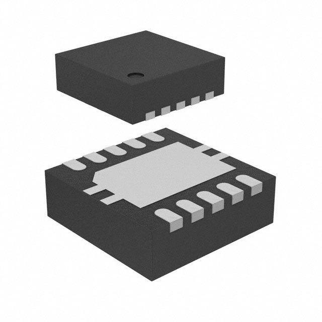
| 产品图片 |
|
| rohs | 符合RoHS无铅 / 符合限制有害物质指令(RoHS)规范要求 |
| 产品系列 | 电源管理 IC,稳压器—开关式稳压器,Texas Instruments TPS62404DRCR- |
| 数据手册 | |
| 产品型号 | TPS62404DRCR |
| PWM类型 | 电压模式 |
| 产品种类 | 稳压器—开关式稳压器 |
| 供应商器件封装 | 10-SON(3x3) |
| 关闭 | Shutdown |
| 其它名称 | 296-27461-1 |
| 制造商产品页 | http://www.ti.com/general/docs/suppproductinfo.tsp?distId=10&orderablePartNumber=TPS62404DRCR |
| 包装 | 剪切带 (CT) |
| 同步整流器 | 是 |
| 商标 | Texas Instruments |
| 安装类型 | 表面贴装 |
| 安装风格 | SMD/SMT |
| 封装 | Reel |
| 封装/外壳 | 10-VFDFN 裸露焊盘 |
| 封装/箱体 | VSON-10 |
| 工作温度 | -40°C ~ 85°C |
| 工作温度范围 | - 40 C to + 85 C |
| 工厂包装数量 | 3000 |
| 开关频率 | 2.25 MHz |
| 拓扑结构 | Buck |
| 最大工作温度 | + 85 C |
| 最大输入电压 | 6 V |
| 最小工作温度 | - 40 C |
| 最小输入电压 | 2.5 V |
| 标准包装 | 1 |
| 电压-输入 | 2.5 V ~ 6 V |
| 电压-输出 | 3.3V,1.2 V ~ 1.9 V |
| 电流-输出 | 400mA,600mA |
| 电源电压-最小 | 2.5 V |
| 电源电流 | 32 uA |
| 类型 | 降压(降压) |
| 系列 | TPS62404 |
| 负载调节 | 0.5 % / A |
| 输入电压 | 2.5 V to 6 V |
| 输出数 | 2 |
| 输出电压 | 1.9 V, 3.3 V |
| 输出电流 | 400 mA, 600 mA |
| 输出端数量 | 2 Output |
| 输出类型 | 固定和可调 |
| 频率-开关 | 2.25MHz |


- 商务部:美国ITC正式对集成电路等产品启动337调查
- 曝三星4nm工艺存在良率问题 高通将骁龙8 Gen1或转产台积电
- 太阳诱电将投资9.5亿元在常州建新厂生产MLCC 预计2023年完工
- 英特尔发布欧洲新工厂建设计划 深化IDM 2.0 战略
- 台积电先进制程称霸业界 有大客户加持明年业绩稳了
- 达到5530亿美元!SIA预计今年全球半导体销售额将创下新高
- 英特尔拟将自动驾驶子公司Mobileye上市 估值或超500亿美元
- 三星加码芯片和SET,合并消费电子和移动部门,撤换高东真等 CEO
- 三星电子宣布重大人事变动 还合并消费电子和移动部门
- 海关总署:前11个月进口集成电路产品价值2.52万亿元 增长14.8%


PDF Datasheet 数据手册内容提取
Product Sample & Technical Tools & Support & Folder Buy Documents Software Community TPS62400,TPS62401 TPS62402,TPS62403,TPS62404 SLVS681F–JUNE2006–REVISEDAUGUST2014 TPS6240x 2.25-MHz 400-mA and 600-mA Dual Step-Down Converter In Small 3-mm x 3-mm VSON Package 1 Features 3 Description • HighEfficiency—Upto95% The TPS6240x family of devices are synchronous 1 dual step-down DC-DC converters optimized for • V RangeFrom2.5Vto6V IN battery-powered portable applications. The devices • 2.25-MHzFixedFrequencyOperation provide two independent output voltage rails powered • OutputCurrentof400mAand600mA by 1-cell Li-Ion or 3-cell NiMH/NiCD batteries. The devices are also suitable to operate from a standard • AdjustableOutputVoltageFrom0.6VtoV IN 3.3-Vor5-Vvoltagerail. • Pin-SelectableOutputVoltageSupportsSimple With an input voltage range from 2.5 V to 6 V, the DynamicVoltageScaling TPS6240x is ideal to power portable applications like • EasyScale™OptionalOne-PinSerialInterface smartphones,PDAs,andotherportableequipment. • PowerSaveModeatLightLoadCurrents With the EasyScale serial interface the output • 180° Out-of-PhaseOperation voltages can be modified during operation. The fixed • OutputVoltageAccuracyinPWMMode±1% output voltage versions TPS62401, TPS62402, • Typical32-μAQuiescentCurrentforBoth TPS62403, and TPS62404 support one-pin controlled simple Dynamic Voltage Scaling for low-power Converters processors. • 100%DutyCycleforLowestDropout The TPS6240x operates at a 2.25-MHz fixed • Availableina10-PinVSON(3mm ×3mm) switching frequency and enters the power save mode operation at light load currents to maintain high 2 Applications efficiency over the entire load current range. For low • CellPhones,SmartPhones noise applications the devices can be forced into • PDAs,PocketPCs fixed frequency PWM mode by pulling the MODE/DATA pin high. In the shutdown mode, the • OMAP™andLow-PowerDSPSupply current consumption is reduced to 1.2 μA, typical. • PortableMediaPlayers The devices allow the use of small inductors and • DigitalRadios capacitorstoachieveasmallsolutionsize. • DigitalCameras The TPS6240x is available in a 10-pin leadless package(3-mm× 3-mmVSON) DeviceInformation(1) PARTNUMBER PACKAGE BODYSIZE(NOM) TPS6240x VSON(10) 3.00mmx3.00mm (1) For all available packages, see the orderable addendum at theendofthedatasheet. SimplifiedSchematic EfficiencyvsOutputCurrent TPS62401 VIN 2.5 V–6 V VIN FB 1 100 10mF 2.2mH Vout1: 1.575 V 90 SW1 400 mA 80 DEF_1 10mF 70 VOUT2= 1.8 V EN_1 VIN= 3.6 V EN_2 SW2 2.2mH Vout2: 1.8 V Efficiency 456000 VOUT1=M 1O.5D7E5/ DVATA= 0 600 mA MODE/ 30 DATA 10mF ADJ2 20 10 GND 0 0.01 0.1 1 10 100 1000 IOUTmA 1 An IMPORTANT NOTICE at the end of this data sheet addresses availability, warranty, changes, use in safety-critical applications, intellectualpropertymattersandotherimportantdisclaimers.PRODUCTIONDATA.
TPS62400,TPS62401 TPS62402,TPS62403,TPS62404 SLVS681F–JUNE2006–REVISEDAUGUST2014 www.ti.com Table of Contents 1 Features.................................................................. 1 8.4 DeviceFunctionalModes........................................13 2 Applications........................................................... 1 8.5 Programming...........................................................14 3 Description............................................................. 1 9 ApplicationandImplementation........................ 22 4 RevisionHistory..................................................... 2 9.1 ApplicationInformation............................................22 9.2 TypicalApplications................................................22 5 DeviceOptions....................................................... 3 10 PowerSupplyRecommendations..................... 32 6 PinConfigurationandFunctions......................... 3 11 Layout................................................................... 33 7 Specifications......................................................... 4 11.1 LayoutGuidelines.................................................33 7.1 AbsoluteMaximumRatings......................................4 11.2 LayoutExample....................................................33 7.2 HandlingRatings.......................................................4 12 DeviceandDocumentationSupport................. 35 7.3 RecommendedOperatingConditions.......................5 7.4 ThermalInformation..................................................5 12.1 DeviceSupport......................................................35 7.5 ElectricalCharacteristics...........................................5 12.2 RelatedLinks........................................................35 7.6 TypicalCharacteristics..............................................7 12.3 Trademarks...........................................................35 12.4 ElectrostaticDischargeCaution............................35 8 DetailedDescription.............................................. 9 12.5 Glossary................................................................35 8.1 Overview...................................................................9 13 Mechanical,Packaging,andOrderable 8.2 FunctionalBlockDiagram.......................................10 Information........................................................... 35 8.3 FeatureDescription.................................................11 4 Revision History ChangesfromRevisionE(April2010)toRevisionF Page • AddedHandlingRatingtable,FeatureDescriptionsection,DeviceFunctionalModes,Applicationand Implementationsection,PowerSupplyRecommendationssection,Layoutsection,DeviceandDocumentation Supportsection,andMechanical,Packaging,andOrderableInformationsection................................................................ 1 ChangesfromRevisionD(February2006)toRevisionE Page • AddedTPS62404device........................................................................................................................................................ 1 • AddedTPS62404devicetoOrderingInformationtable......................................................................................................... 1 • AddedTPS62404devicetoAddressableRegisterstable.................................................................................................... 15 • AddedTPS62404deviceto'SelectableOutputVoltagesforConverter1'table................................................................. 19 • AddedTPS62404deviceto'SelectableOutputVoltagesforConverter2'table................................................................. 21 • AddedTPS62404deviceto'ApplicationInformation'section.............................................................................................. 23 • AddedTPS62404deviceefficiencygraph(Figure22)......................................................................................................... 26 2 SubmitDocumentationFeedback Copyright©2006–2014,TexasInstrumentsIncorporated ProductFolderLinks:TPS62400 TPS62401TPS62402 TPS62403 TPS62404
TPS62400,TPS62401 TPS62402,TPS62403,TPS62404 www.ti.com SLVS681F–JUNE2006–REVISEDAUGUST2014 5 Device Options T PARTNUMBER DEFAULTOUTPUTVOLTAGE(1) OUTPUTCURRENT A OUT1 400mA TPS62400 Adjustable OUT2 600mA Fixed DEF_1=High1.1V OUT1 400mA TPS62401 default DEF_1=Low1.575V OUT2 Fixeddefault1.8V 600mA Fixed DEF_1=High1.8V OUT1 400mA TPS62402 default DEF_1=Low1.2V –40°Cto85°C OUT2 Fixeddefault3.3V 600mA Fixed DEF_1=High1.1V OUT1 400mA TPS62403 default DEF_1=Low1.575V OUT2 Fixeddefault2.8V 600mA Fixed DEF_1=High1.9V OUT1 400mA TPS62404 default DEF_1=Low1.2V OUT2 Fixeddefault3.3V 600mA (1) ContactTIforotherfixedoutputvoltageoptions. 6 Pin Configuration and Functions DRCPackage 10Pins TopView ADJ2 1 10 SW2 MODE/DATA 2 AD 9 EN2 P VIN 3 wer 8 GND o FB1 4 P 7 EN1 DEF_1 5 6 SW1 PinFunctions PIN I/O DESCRIPTION NAME NO. Inputtoadjustoutputvoltageofconverter2.Inadjustableversion(TPS62400)connectaexternal resistordividerbetweenVOUT2,thispinandGNDtosetoutputvoltagebetween0.6VandVIN.At ADJ2 1 I fixedoutputvoltageversion(TPS62401,TPS62402,TPS62403,TPS62404)thispinMUSTbedirectly connectedtotheoutput.IfEasyScaleInterfaceisusedforconverter2,thispinmustbedirectly connectedtotheoutput,too. Thispindefinestheoutputvoltageofconverter1.Thepinactseitherasanaloginputforoutput voltagesettingviaexternalresistors(TPS62400),ordigitalinputtoselectbetweentwofixeddefault outputvoltages(TPS62401,TPS62402,TPS62403,TPS62404). DEF_1 5 I FortheTPS62400,anexternalresistornetworkneedstobeconnectedtothispintoadjustthedefault outputvoltage. Usingthefixedoutputvoltagedeviceoptionsthispinselectsbetweentwofixeddefaultoutput voltages,seetableorderinginformation EN1 7 I EnableInputforConverter1,activehigh EN2 9 I EnableInputforConverter2,activehigh Directfeedbackvoltagesenseinputofconverter1,connectdirectlytoVout1.Aninternalfeed FB1 4 I forwardcapacitorisconnectedbetweenthispinandtheerroramplifier.Incaseoffixedoutputvoltage versionsorwhentheInterfaceisused,thispinisconnectedtoaninternalresistordividernetwork. GND 8 GNDforbothconverters;connectthispintothePowerPAD™ Copyright©2006–2014,TexasInstrumentsIncorporated SubmitDocumentationFeedback 3 ProductFolderLinks:TPS62400 TPS62401TPS62402 TPS62403 TPS62404
TPS62400,TPS62401 TPS62402,TPS62403,TPS62404 SLVS681F–JUNE2006–REVISEDAUGUST2014 www.ti.com PinFunctions(continued) PIN I/O DESCRIPTION NAME NO. ThisPinhas2functions: OperationModeselection:Withlowlevel,PowerSaveModeisenabledwherethedevice 1. operatesinPFMmodeatlightloadsandentersautomaticallyPWMmodeatheavyloads. MODE/DA PullingthisPINtohighforcesthedevicetooperateinPWMmodeoverthewholeloadrange. 2 I/O TA EasyScale™Interfacefunction:Onewireserialinterfacetochangetheoutputvoltageofboth converters.Thepinhasanopendrainoutputtoprovideanacknowledgeconditionif 2. requested.Thecurrentintotheopendrainoutputstagemaynotexceed500μA.Theinterface isactiveifeitherEN1orEN2ishigh. PowerPA ConnecttoGND D™ SW1 6 I/O SwitchPinofConverter1.ConnecttoInductor SW2 10 I/O SwitchPinofConverter2.ConnecttoInductor. VIN 3 Supplyvoltage,connecttoVBAT,2.5Vto6V 7 Specifications 7.1 Absolute Maximum Ratings overoperatingfree-airtemperaturerange(unlessotherwisenoted)(1) MIN MAX UNIT InputvoltagerangeonV (2) –0.3 7 V IN VoltagerangeonEN,MODE/DATA,DEF_1 –0.3 V +0.3,≤ V IN 7 currentintoMODE/DATA ≤0.5 mA VoltageonSW1,SW2 –0.3 7 V VoltageonADJ2,FB1 –0.3 V +0.3,≤ V IN 7 T(max) Maximumoperatingjunctiontemperature 150 °C J T Operatingambienttemperaturerange –40 85 °C A (1) Stressesbeyondthoselistedunderabsolutemaximumratingsmaycausepermanentdamagetothedevice.Thesearestressratings only,andfunctionaloperationofthedeviceattheseoranyotherconditionsbeyondthoseindicatedunderrecommendedoperating conditionsisnotimplied.Exposuretoabsolute–maximum–ratedconditionsforextendedperiodsmayaffectdevicereliability. (2) Allvoltagevaluesarewithrespecttonetworkgroundterminal. 7.2 Handling Ratings MIN MAX UNIT T Storagetemperaturerange –65 150 °C stg Humanbodymodel(HBM),perANSI/ESDA/JEDECJS-001,all 1 pins(2) kV V Electrostaticdischarge(1) Chargeddevicemodel(CDM),perJEDECspecification 0.5 (ESD) JESD22-C101,allpins(3) Machinemodel 200 V (1) Thehumanbodymodelisa100pFcapacitordischargedthrougha1.5kΩresistorintoeachpin.Themachinemodelisa200pF capacitordischargeddirectlyintoeachpin. (2) JEDECdocumentJEP155statesthat500-VHBMallowssafemanufacturingwithastandardESDcontrolprocess. (3) JEDECdocumentJEP157statesthat250-VCDMallowssafemanufacturingwithastandardESDcontrolprocess. 4 SubmitDocumentationFeedback Copyright©2006–2014,TexasInstrumentsIncorporated ProductFolderLinks:TPS62400 TPS62401TPS62402 TPS62403 TPS62404
TPS62400,TPS62401 TPS62402,TPS62403,TPS62404 www.ti.com SLVS681F–JUNE2006–REVISEDAUGUST2014 7.3 Recommended Operating Conditions overoperatingfree-airtemperaturerange(unlessotherwisenoted) MIN NOM MAX UNIT VIN Supplyvoltage 2.5 6 V VOUT Outputvoltagerangeforadjustablevoltage 0.6 VIN V T Operatingambienttemperature -40 85 °C A T Operatingjunctiontemperature -40 125 °C J 7.4 Thermal Information TPS6240x THERMALMETRIC(1) VSON UNIT 10PINS R Junction-to-ambientthermalresistance 45.9 θJA R Junction-to-case(top)thermalresistance 64.3 θJC(top) R Junction-to-boardthermalresistance 20.4 θJB °C/W ψ Junction-to-topcharacterizationparameter 1.3 JT ψ Junction-to-boardcharacterizationparameter 20.6 JB R Junction-to-case(bottom)thermalresistance 2.8 θJC(bot) (1) Formoreinformationabouttraditionalandnewthermalmetrics,seetheICPackageThermalMetricsapplicationreport,SPRA953. 7.5 Electrical Characteristics V =3.6V,V =1.8V,EN=V ,MODE=GND,L=2.2μH,C =20μF,T =–40°Cto85°Ctypicalvaluesareat IN OUT IN OUT A T =25°C(unlessotherwisenoted) A PARAMETER TESTCONDITIONS MIN TYP MAX UNIT SUPPLYCURRENT V Inputvoltagerange 2.5 6.0 V IN Oneconverter,I =0mA.PFMmode 19 29 μA OUT enabled(Mode=0)devicenotswitching, EN1=1OREN2=1 Twoconverter,I =0mA.PFMmode 32 48 μA OUT enabled(Mode=0)devicenotswitching, IQ Operatingquiescentcurrent EN1=1ANDEN2=1 I =0mA,MODE/DATA=GND,forone 23 μA OUT converter,V 1.575V(1) OUT I =0mA,MODE/DATA=V ,forone 3.6 mA OUT IN converter,V 1.575V (1) OUT EN1,EN2=GND,V =3.6V(2) 1.2 3 IN ISD Shutdowncurrent EN1,EN2=GND,VINrampedfrom0Vto 0.1 1 μA 3.6V(3) Falling 1.5 2.35 V Undervoltagelockoutthreshold V UVLO Rising 2.4 ENABLEEN1,EN2 V High-levelinputvoltagerange,EN1, 1.2 V V IH IN EN2 V Low-levelinputvoltagerange,EN1, 0 0.4 V IL EN2 I Inputbiascurrent,EN1,EN2 EN1,EN2=GNDorVIN 0.05 1.0 μA IN (1) Deviceisswitchingwithnoloadontheoutput,L=3.3μH,valueincludeslossesofthecoil (2) Thesevaluesarevalidafterthedevicehasbeenalreadyenabledonetime(EN1orEN2=high)andsupplyvoltageV hasnot IN powereddown. (3) Thesevaluesarevalidwhenthedeviceisdisabled(EN1andEN2low)andsupplyvoltageV ispoweredup.Thevaluesremainvalid IN untilthedevicehasbeenenabledfirsttime(EN1orEN2=high).Afterfirstenable,Note3becomesvalid. Copyright©2006–2014,TexasInstrumentsIncorporated SubmitDocumentationFeedback 5 ProductFolderLinks:TPS62400 TPS62401TPS62402 TPS62403 TPS62404
TPS62400,TPS62401 TPS62402,TPS62403,TPS62404 SLVS681F–JUNE2006–REVISEDAUGUST2014 www.ti.com Electrical Characteristics (continued) V =3.6V,V =1.8V,EN=V ,MODE=GND,L=2.2μH,C =20μF,T =–40°Cto85°Ctypicalvaluesareat IN OUT IN OUT A T =25°C(unlessotherwisenoted) A PARAMETER TESTCONDITIONS MIN TYP MAX UNIT DEF_1INPUT V DEF_1highlevelinputvoltagerange VOUT1=fixedoutputvoltageoption 0.9 V V DEF_1H IN V DEF_1lowlevelinputvoltagerange VOUT1=fixedoutputvoltageoption 0 0.4 V DEF_1L I InputbiascurrentDEF_1 DEF_1GNDorVIN 0.01 1.0 μA IN MODE/DATA V High-levelinputvoltagerange, 1.2 V V IH IN MODE/DATA V Low-levelinputvoltagerange, 0 0.4 V IL MODE/DATA I Inputbiascurrent,MODE/DATA MODE/DATA=GNDorVIN 0.01 1.0 μA IN V Acknowledgeoutputvoltagehigh Opendrain,viaexternalpullupresistor V V OH IN V Acknowledgeoutputvoltagelow Opendrain,sinkcurrent500μA 0 0.4 V OL INTERFACETIMING t Starttime 2 μs Start t Hightimelowbit,logic0detection SignallevelonMODE/DATApinis>1.2V 2 200 μs H_LB 2x t Lowtimelowbit,logic0detection SignallevelonMODE/DATApin<0.4V 400 μs L_LB t H_LB t Lowtimehighbit,logic1detection SignallevelonMODE/DATApin<0.4V 2 200 μs L_HB 2x t Hightimehighbit,logic1detection SignallevelonMODE/DATApinis>1.2V 400 μs H_HB t L_HB T EndofStream T 2 μs EOS EOS Durationofacknowledgecondition t (MODE/DATElinepulledlowbythe V 2.5Vto6V 400 520 μs ACKN IN device) t Acknowledgevalidtime 2 μs valACK t Timeoutforenteringpowersavemode MODE/DATAPinchangesfromhightolow 520 μs timeout POWERSWITCH P-ChannelMOSFETon-resistance, R V =V =3.6V 280 620 mΩ DS(ON) Converter1,2 IN GS I P-Channelleakagecurrent V =6.0V 1 μA LK_PMOS DS N-ChannelMOSFETon-resistance R V =V =3.6V 200 450 mΩ DS(ON) Converter1,2 IN GS IncludesN-Chanelleakagecurrent, ILK_SW1/SW2 LeakagecurrentintoSW1/SW2pin V =open,V =6.0V,EN=GND(4) 6 7.5 μA IN SW ForwardCurrentLimit OUTPUT1 0.68 0.8 0.92 I 2.5V≤V ≤6.0V A LIMF PMOSandNMOS OUTPUT2 IN 0.85 1.0 1.15 T Thermalshutdown Increasingjunctiontemperature 150 °C SD Thermalshutdownhysteresis Decreasingjunctiontemperature 20 °C OSCILLATOR fSW Oscillatorfrequency 2.5V≤VIN≤6V 2.0 2.25 2.5 MHz (4) OnpinsSW1andSW2aninternalresistorof1MΩisconnectedtoGND. 6 SubmitDocumentationFeedback Copyright©2006–2014,TexasInstrumentsIncorporated ProductFolderLinks:TPS62400 TPS62401TPS62402 TPS62403 TPS62404
TPS62400,TPS62401 TPS62402,TPS62403,TPS62404 www.ti.com SLVS681F–JUNE2006–REVISEDAUGUST2014 Electrical Characteristics (continued) V =3.6V,V =1.8V,EN=V ,MODE=GND,L=2.2μH,C =20μF,T =–40°Cto85°Ctypicalvaluesareat IN OUT IN OUT A T =25°C(unlessotherwisenoted) A PARAMETER TESTCONDITIONS MIN TYP MAX UNIT OUTPUT V Adjustableoutputvoltagerange 0.6 V V OUT IN V Referencevoltage 600 mV ref Voltagepositioningactive, MODE/DATA=GND, 1.01 V –1.5% 2.5% OUT(PFM) deviceoperatinginPFMmode, V OUT VIN=2.5Vto5.0V (6) (7) MODE/DATA=GND; DCoutputvoltageaccuracyadjustable andfixedoutputvoltage(5) dVeINvic=e2o.5pVeratotin6g.0iVn(7P)WMMode, –1% 0% 1% V =2.5Vto6.0V,Mode/Data=V , V IN IN OUT(PWM) FixedPWMoperation, –1% 0% 1% 0mA<I <400mA;0mA<I < OUT1 OUT2 600mA(8) DCoutputvoltageloadregulation PWMoperationmode 0.5 %/A t Start-uptime Activationtimetostartswitching(9) 170 μs Startup t V RampUPtime Timetorampfrom5%to95%ofV 750 μs Ramp OUT OUT (5) Outputvoltagespecificationdoesnotincludetoleranceofexternalvoltageprogrammingresistors (6) ConfigurationLtyp2.2μH,C typ20μF,seeparametermeasurementinformation,theoutputvoltagerippleinPFMmodedependson OUT theeffectivecapacitanceoftheoutputcapacitor,largeroutputcapacitorsleadtotighteroutputvoltagetolerance. (7) InPowerSaveMode,PWMoperationistypicallyenteredatI =V /32Ω. PSM IN (8) ForV >2V,V min=V +0.5V OUT IN OUT (9) Thistimeisvalidifoneconverterturnsfromshutdownmode(EN2=0)toactivemode(EN2=1)ANDtheotherconverterisalready enabled(e.g.,EN1=1).Incasebothconvertersareturnedfromshutdownmode(EN1andEN2=low)toactivemode(EN1and/or EN2=1)avalueoftyp80μsforrampupofinternalcircuitsneedstobeadded.Aftert theconverterstartsswitchingandramps Start V . OUT 7.6 Typical Characteristics 2.5 24 2.45 23 2.4 85°C 2.35 22 sc - MHz 2.22.53 -40°C q -Am 21 25°C o d F 2.2 Id 20 25°C -40°C 2.15 19 85°C 2.1 18 2.05 2 17 2.5 3 3.5 4 4.5 5 5.5 6 2.5 3 3.5 4 4.5 5 5.5 6 VIN- V VIN- V Figure1.FOSCvsVIN Figure2.IqForOneConverter,NotSwitching Copyright©2006–2014,TexasInstrumentsIncorporated SubmitDocumentationFeedback 7 ProductFolderLinks:TPS62400 TPS62401TPS62402 TPS62403 TPS62404
TPS62400,TPS62401 TPS62402,TPS62403,TPS62404 SLVS681F–JUNE2006–REVISEDAUGUST2014 www.ti.com Typical Characteristics (continued) 42 0.55 40 0.5 0.45 38 85°C 0.4 A 36 W Iddq -m 34 25°C RDSon - 0.03.53 85°C 25°C 32 -40°C 0.25 30 0.2 -40°C 28 0.15 2.5 3 3.5 4 4.5 5 5.5 6 2.5 3 3.5 4 4.5 5 5.5 6 VIN- V VIN- V Figure3.IqForBothConverters,NotSwitching Figure4.RDSONPMOSvsVIN 0.3 0.25 0.2 85°C W on - 25°C S RD 0.15 -40°C 0.1 0.05 2.5 3 3.5 4 4.5 5 5.5 6 VIN- V Figure5.R NMOSvsV DSON IN 8 SubmitDocumentationFeedback Copyright©2006–2014,TexasInstrumentsIncorporated ProductFolderLinks:TPS62400 TPS62401TPS62402 TPS62403 TPS62404
TPS62400,TPS62401 TPS62402,TPS62403,TPS62404 www.ti.com SLVS681F–JUNE2006–REVISEDAUGUST2014 8 Detailed Description 8.1 Overview The TPS62400 includes two synchronous step-down converters. The converters operate with typically 2.25MHz fixed frequency pulse width modulation (PWM) at moderate to heavy load currents. If Power Safe Mode is enabled, the converters automatically enter Power Save Mode at light load currents and operate in PFM (Pulse FrequencyModulation). During PWM operation the converters use a unique fast response voltage mode controller scheme with input voltage feed-forward to achieve good line and load regulation allowing the use of small ceramic input and output capacitors. At the beginning of each clock cycle initiated by the clock signal, the P-channel MOSFET switch is turnedonandtheinductorcurrentrampsupuntilthecomparatortripsandthecontrollogicturnsofftheswitch. Each converter integrates two current limits, one in the P-channel MOSFET and another one in the N-channel MOSFET. When the current in the P-channel MOSFET reaches its current limit, the P-channel MOSFET is turned off and the N-channel MOSFET is turned on. If the current in the N-channel MOSFET is above the N- MOScurrentlimitthreshold,theN-channelMOSFETremainsonuntilthecurrentdropsbelowitscurrentlimit. The two DC-DC converters operate synchronized to each other. A 180° phase shift between converter 1 and converter2decreasestheinputRMScurrent. Copyright©2006–2014,TexasInstrumentsIncorporated SubmitDocumentationFeedback 9 ProductFolderLinks:TPS62400 TPS62401TPS62402 TPS62403 TPS62404
TPS62400,TPS62401 TPS62402,TPS62403,TPS62404 SLVS681F–JUNE2006–REVISEDAUGUST2014 www.ti.com 8.2 Functional Block Diagram VIN Converter 1 PMOS Current Limit Comparator VIN FB_VOUT Thermal Shutdown Softstart VREF +1% SkipComp. EN1 FB_VOUT VREF- 1% SkipComp. Low Ext.res.network VREF Control Gate Driver ErrorAmp. Stage DEF1 INnet.t wRoerskistor FVBOUT1 Icnotmerpneanlsated PCWomMp. SW1 C 25pF ff MODE RI 1 Register Sawtooth R DEF1_High Generator GND FB1 RI..N I3 DEF1_Low Average Current Detector Note 1 SkipMode Entry NMOS Current Limit Comparator CLK 0° Reference 2.25MHz Load Comparator EasyScale Mode/ Oscillator Interface DATA ACK Undervoltage CLK 180° PMOS Current MOSFET Lockout Limit Comparator Open drain VIN Converter 2 FB_VOUT Int. Resistor VREF +1% Network SkipComp. Register FB_VOUT DEF2 Note 2 VREF- 1% VREF SkipComp. Low Control Gate Driver Cff25pF ErrorAmp. Stage RI 1 Internal compensated PWM RI..N Comp. SW2 MODE FB_VOUT2 ADJ2 Sawtooth Generator GND Thermal Average Shutdown Current Detector SkipMode Entry NMOS Current Softstart CLK 180° Limit Comparator EN2 Load Comparator GND (1) In fixed output voltage version, the PIN DEF_1 is connected to an internal digital input and disconnected from the erroramplifier (2) TosettheoutputvoltageofConverter2viaEasyScale™Interface,ADJ2pinmustbedirectlyconnectedtoVOUT2 10 SubmitDocumentationFeedback Copyright©2006–2014,TexasInstrumentsIncorporated ProductFolderLinks:TPS62400 TPS62401TPS62402 TPS62403 TPS62404
TPS62400,TPS62401 TPS62402,TPS62403,TPS62404 www.ti.com SLVS681F–JUNE2006–REVISEDAUGUST2014 8.3 Feature Description 8.3.1 Converter1 In the adjustable output voltage version TPS62400, the converter 1 default output voltage can be set via an external resistor network on PIN DEF_1, which operates as an analog input. In this case, the output voltage can be set in the range of 0.6V to VIN V. The FB1 Pin must be directly connected to the converter 1 output voltage V .Itfeedsbacktheoutputvoltagedirectlytotheregulationloop. OUT1 The output voltage of converter 1 can also be changed by the EasyScale™ serial Interface. This makes the deviceveryflexibleforoutputvoltageadjustment.Inthiscase,thedeviceusesaninternalresistornetwork. In the fixed default output voltage version TPS62401, the DEF_1 Pin is configured as a digital input. The converter 1 defaults to 1.1V or 1.575V depending on the level of DEF_1 pin. If DEF_1 is low the default is 1.575V; if high, the default is 1.1V. With the EasyScale™ interface, the output voltage for each DEF_1 Pin condition(highorlow)canbechanged. 8.3.2 Converter2 In the adjustable output voltage version TPS62400, the converter 2 output voltage is set by an external resistor dividerconnectedtoADJ2Pinandusesanexternalfeedforwardcapacitorof33pF. In fixed output voltage version TPS62401, the default output voltage is fixed to 1.8V. In this case, the ADJ2 pin mustbeconnecteddirectlytotheconverter2outputvoltageV . OUT2 It is also possible to change the output voltage of converter 2 via the EasyScale™ Interface. In this case, the ADJ2 Pin must be directly connected to converter 2 output voltage V and no external resistors may be OUT2 connected. 8.3.3 DEF_1PinFunction The DEF_1 pin is dedicated to converter 1 and makes the output voltage selection very flexible to support dynamicvoltagemanagement. Dependingonthedeviceversion,thispinworkseitheras: 1. Analoginputforadjustableoutputvoltagesetting(TPS62400): – Connecting an external resistor network to this pin adjusts the default output voltage to any value starting from0.6VtoV IN 2. Digitalinputforfixeddefaultoutputvoltageselection(TPS62401): – In case this pin is tied to low level, the output voltage is set according to the value in register REG_DEF_1_Low. The default voltage will be 1.575V. If tied to high level, the output voltage is set according to the value in register REG_DEF_1_High. The default value in this case is 1.1V. Depending on the level of Pin DEF_1, it selects between the two registers REG_DEF_1_Low and REG_DEF_1_High for output voltage setting. Each register content (and therefore output voltage) can be changed individually via the EasyScale™ interface. This makes the device very flexible in terms of output voltage setting;seeTable4. 8.3.4 ModeSelection The MODE/DATA pin allows mode selection between forced PWM Mode and Power Save Mode for both converters. Furthermore, this pin is a multipurpose pin and provides (besides Mode selection) a one-pin interface to receive serial data from a host to set the output voltage. This is described in the EasyScale™ Interface section. Connecting this pin to GND enables the automatic PWM and power save mode operation. The converters operates in fixed-frequency PWM mode at moderate-to-heavy loads, and in the PFM mode during light loads, maintaininghighefficiencyoverawideloadcurrentrange. Pulling the MODE/DATA pin high forces both converters to operate constantly in the PWM mode, even at light load currents. The advantage is that the converters operate with a fixed frequency, allowing simple filtering of the switching frequency for noise-sensitive applications. In this mode, the efficiency is lower compared to the power save mode during light loads. For additional flexibility, it is possible to switch from power save mode to forced PWMmodeduringoperation.Thisallowsefficientpowermanagementbyadjustingtheoperationoftheconverter tothespecificsystemrequirements. Copyright©2006–2014,TexasInstrumentsIncorporated SubmitDocumentationFeedback 11 ProductFolderLinks:TPS62400 TPS62401TPS62402 TPS62403 TPS62404
TPS62400,TPS62401 TPS62402,TPS62403,TPS62404 SLVS681F–JUNE2006–REVISEDAUGUST2014 www.ti.com Feature Description (continued) In case the operation mode is changed from forced PWM mode (MODE/DATA = high) to Power Save Mode Enable(MODE/DATA=0),thePowerSaveModeisenabledafteradelaytimeoft ,whichismax.520μs. timeout TheforcedPWMModeoperationisenabledimmediatelywithPinMODE/DATAsetto1. 8.3.5 Enable The device has a separate EN pin for each converter to start up each converter independently. If EN1 and EN2 aresettohigh,thecorrespondingconverterstartsupwithsoftstartaspreviouslydescribed. Pulling EN1 and EN2 pin low forces the device into shutdown, with a shutdown quiescent current of typically 1.2μA. In this mode, the P and N-Channel MOSFETs are turned-off and the entire internal control circuitry is switched-off.ForproperoperationtheEN1andEN2pinsmustbeterminatedandmustnotbeleftfloating. 8.3.6 SoftStart The two converters have an internal soft start circuit that limits the inrush current during start-up. During soft start,theoutputvoltagerampupiscontrolledasshowninFigure6. EN 95% 5% VOUT t t Startup RAMP Figure6. SoftStart 8.3.7 Short-CircuitProtection Both outputs are short-circuit protected with maximum output current = I (P-MOS and N-MOS). Once the LIMF PMOS switch reaches its current limit, it is turned off and the NMOS switch is turned on. The PMOS only turns onagain,oncethecurrentintheNMOSdecreasesbelowtheNMOScurrentlimit. 8.3.8 Under-VoltageLockout The under-voltage lockout circuit prevents the device from malfunctioning at low input voltages, and from excessive discharge of the battery, and disables the converters. The under-voltage lockout threshold is typically 1.5V; maximum of 2.35V. In case the default register values are overwritten by the Interface, the new values in the registers REG_DEF_1_High, REG_DEF_1_Low and REG_DEF_2 remain valid as long the supply voltage doesnotfallbelowtheunder-voltagelockoutthreshold,independentofwhethertheconvertersaredisabled. 8.3.9 ThermalShutdown As soon as the junction temperature, T , exceeds 150°C (typical) the device goes into thermal shutdown. In this J mode, the P and N-Channel MOSFETs are turned-off. The device continues its operation when the junction temperaturefallsbelowthethermalshutdownhysteresis. 12 SubmitDocumentationFeedback Copyright©2006–2014,TexasInstrumentsIncorporated ProductFolderLinks:TPS62400 TPS62401TPS62402 TPS62403 TPS62404
TPS62400,TPS62401 TPS62402,TPS62403,TPS62404 www.ti.com SLVS681F–JUNE2006–REVISEDAUGUST2014 8.4 Device Functional Modes 8.4.1 PowerSaveMode The Power Save Mode is enabled with MODE/DATA Pin set to low for both converters. If the load current of a converter decreases, this converter will enter Power Save Mode operation automatically. The transition to Power SaveModeofaconverterisindependentfromtheoperatingconditionoftheotherconverter.DuringPowerSave Mode the converter operates with reduced switching frequency in PFM mode and with a minimum quiescent current to maintain high efficiency. The converter will position the output voltage in PFM mode to typically 1.01×V .Thisvoltagepositioningfeatureminimizesvoltagedropscausedbyasuddenloadstep. OUT In order to optimize the converter efficiency at light load the average inductor current is monitored. The device changes from PWM Mode to Power Save Mode, if in PWM mode the inductor current falls below a certain threshold. The typical output current threshold depends on VIN and can be calculated according to Equation 1 foreachconverter. Equation1:AverageoutputcurrentthresholdtoenterPFMMode VIN I (cid:1) DCDC OUT_PFM_enter 32(cid:1) (1) Equation2:AverageoutputcurrentthresholdtoleavePFMMode VIN I (cid:1) DCDC OUT_PFM_leave 24(cid:1) (2) In order to keep the output voltage ripple in Power Save Mode low, the output voltage is monitored with a single threshold comparator (skip comparator). As the output voltage falls below the skip comparator threshold (skip comp) of 1.01 x VOUTnominal, the corresponding converter starts switching for a minimum time period of typ. 1μs and provides current to the load and the output capacitor. Therefore the output voltage will increase and the device maintains switching until the output voltage trips the skip comparator threshold (skip comp) again. At this moment all switching activity is stopped and the quiescent current is reduced to minimum. The load is supplied by the output capacitor until the output voltage has dropped below the threshold again. Hereupon the device startsswitchingagain. The Power Save Mode is left and PWM Mode entered in case the output current exceeds the current IOUT_PFM_leave or if the output voltage falls below a second comparator threshold, called skip comparator low (Skip Comp Low) threshold. This skip comparator low threshold is set to -2% below nominal Vout, and enables a fasttransitionfromPowerSaveModetoPWMModeduringaloadstep. In Power Save Mode the quiescent current is reduced typically to 19μA for one converter and 32μA for both convertersactive.ThissingleskipcomparatorthresholdmethodinPowerSaveModeresultsinaverylowoutput voltage ripple. The ripple depends on the comparator delay and the size of the output capacitor. Increasing output capacitor values will minimize the output ripple. The Power Save Mode can be disabled through the MODE/DATA pin set to high. Both converters will then operate in fixed PWM mode. Power Save Mode Enable/Disableappliestobothconverters. 8.4.2 DynamicVoltagePositioning This feature reduces the voltage under/overshoots at load steps from light to heavy load and vice versa. It is activated in Power Save Mode operation. It provides more headroom for both the voltage drop at a load step, andthevoltageincreaseataloadthrow-off.Thisimprovesloadtransientbehavior. At light loads, in which the converter operates in PFM Mode, the output voltage is regulated typically 1% higher than the nominal value. In case of a load transient from light load to heavy load, the output voltage drops until it reaches the skip comparator low threshold set to –2% below the nominal value and enters PWM mode. During a load throw off from heavy load to light load, the voltage overshoot is also minimized due to active regulation turningontheN-channelswitch. Copyright©2006–2014,TexasInstrumentsIncorporated SubmitDocumentationFeedback 13 ProductFolderLinks:TPS62400 TPS62401TPS62402 TPS62403 TPS62404
TPS62400,TPS62401 TPS62402,TPS62403,TPS62404 SLVS681F–JUNE2006–REVISEDAUGUST2014 www.ti.com Device Functional Modes (continued) Smooth increased load Fast load transient +1% PFM Mode PFM Mode light load light load V OUT_NOM PWM Mode PWM Mode PWM Mode medium/heavy load medium/heavy load medium/heavy load COMP_LOW threshold -2% Figure7. DynamicVoltagePositioning 8.4.3 100%DutyCycleLowDropoutOperation The converters offer a low input-to-output voltage difference while still maintaining operation with the use of the 100% duty cycle mode. In this mode the P-channel switch is constantly turned on. This is particularly useful in battery-powered applications to achieve longest operation time by taking full advantage of the whole battery voltagerange.Theminimuminputvoltagetomaintainregulationdependsontheloadcurrentandoutputvoltage, andcanbecalculatedas: Vinmin(cid:3)Voutmax(cid:2)Ioutmax(cid:1)(cid:4)RDSonmax(cid:2)RL(cid:5) (3) with: Iout =maximumoutputcurrentplusinductorripplecurrent max RDSon =maximumP-channelswitchRDSon. max R =DCresistanceoftheinductor L Vout =nominaloutputvoltageplusmaximumoutputvoltagetolerance max With decreasing load current, the device automatically switches into pulse skipping operation in which the power stage operates intermittently based on load demand. By running cycles periodically the switching losses are minimizedandthedevicerunswithaminimumquiescentcurrent,maintaininghighefficiency. 8.4.4 180° Out-Of-PhaseOperation In PWM Mode the converters operate with a 180° turn-on phase shift of the PMOS (high side) transistors. This prevents the high-side switches of both converters from being turned on simultaneously, and therefore smooths theinputcurrent.Thisfeaturereducesthesurgecurrentdrawnfromthesupply. 8.5 Programming 8.5.1 EasyScale™:One-PinSerialInterfaceforDynamicOutputVoltageAdjustment 8.5.1.1 General EasyScale is a simple but very flexible one pin interface to configure the output voltage of both DC-DC converters. The interface is based on a master – slave structure, where the master is typically a microcontroller or application processor. Figure 8 and Table 3. give an overview of the protocol. The protocol consists of a device specific address byte and a data byte. The device specific address byte is fixed to 4E hex. The data byte consists of five bits for information, two address bits, and the RFA bit. RFA bit set to high indicates the Request ForAcknowledgecondition.TheAcknowledgeconditionisonlyappliediftheprotocolwasreceivedcorrectly. The advantage of EasyScale™ compared to other one pin interfaces is that its bit detection is in a large extent independent from the bit transmission rate. It can automatically detect bit rates between 1.7kBit/sec and up to 160kBit/sec.Furthermore,theinterfaceissharedwiththeMODE/DATAPinandrequiresnoadditionalpin. 14 SubmitDocumentationFeedback Copyright©2006–2014,TexasInstrumentsIncorporated ProductFolderLinks:TPS62400 TPS62401TPS62402 TPS62403 TPS62404
TPS62400,TPS62401 TPS62402,TPS62403,TPS62404 www.ti.com SLVS681F–JUNE2006–REVISEDAUGUST2014 Programming (continued) 8.5.1.2 Protocol All bits are transmitted MSB first and LSB last. Figure 9 shows the protocol without acknowledge request (bit RFA=0),Figure10withacknowledge(bitRFA=1)request. Prior to both bytes, device address byte and data byte, a start condition needs to be applied. For this, the MODE/DATA pin need be pulled high for at least t before the bit transmission starts with the falling edge. In Start case the MODE/DATA line was already at high level (forced PWM Mode selection), no start condition need be appliedpriorthedeviceaddressbyte. ThetransmissionofeachbyteneedstobeclosedwithanEndOfStreamconditionforatleastT . EOS 8.5.1.3 AddressableRegisters Three registers with a data content of 5 bits can be addressed. With 5 bit data content, 32 different values for each register are available. Table 1 shows the addressable registers to set the output voltage when DEF_1 pin works as digital input. In this case, converter 1 has a related register for each DEF_1 Pin condition, and one register for converter 2. With a high/low condition on pin DEF_1 (TPS62401) either the content of register REG_DEF_1_high/REG_DEF1_low is selected. The output voltage of converter 1 is set according to the values inTable4. Table 2 shows the addressable registers if DEF_1 pin acts as analog input with external resistors connected. In this case one register is available for each converter. The output voltage of converter 1 is set according to the values in Table 5. For converter 2, the available voltages are shown in Table 6. To generate these output voltages a precise internal resistor divider network is used, making external resistors unnecessary (less board space),andprovideshigheroutputvoltageaccuracy.TheInterfaceisactivatedifatleastoneoftheconvertersis enabled(EN1orEN2ishigh).Afterthestartup-timet (170μs)theinterfaceisreadyfordatareception. Start Table1.AddressableRegistersfordefaultFixedOutputVoltageOptions(PINDEF_1=digitalinput) DEVICE REGISTER DESCRIPTION DEF_1 A1 A0 D4 D3 D2 D1 D0 PIN REG_DEF_1_High Converter1outputvoltagesettingfor High 0 1 Outputvoltagesetting,see DEF_1=Highcondition.Thecontentof Table4 theregisterisactivewithDEF1_Pinhigh. TPS62401, TPS62402, REG_DEF_1_Low Converter1outputvoltagesettingfor Low 0 0 Outputvoltagesetting,see TPS62403, DEF_1=Lowcondition. Table4 TPS62404 REG_DEF_2 Converter2outputvoltage Not 1 0 Outputvoltagesetting,see applicable Table6 Don’tuse 1 1 Table2.AddressableRegistersforAdjustableOutputVoltageOptions(PINDEF_1=analoginput) DEVICE REGISTER DESCRIPTION A1 A0 D4 D3 D2 D1 D0 REG_DEF_1_High notavailable REG_DEF_1_Low Converter1outputvoltagesetting 0 0 seeTable5 TPS62400 REG_DEF_2 Converter2outputvoltage 1 0 seeTable6 Don’t’use 1 1 8.5.1.3.1 BitDecoding The bit detection is based on a PWM scheme, where the criterion is the relation between t and t . It can LOW HIGH besimplifiedto: HighBit:t >t ,butwitht atleast2xt ,seeFigure34 High Low High Low LowBit:t >t ,butwitht atleast2xt ,seeFigure34 Low High Low High The bit detection starts with a falling edge on the MODE/DATA pin and ends with the next falling edge. Dependingontherelationbetweent andt a0or1isdetected. Low High Copyright©2006–2014,TexasInstrumentsIncorporated SubmitDocumentationFeedback 15 ProductFolderLinks:TPS62400 TPS62401TPS62402 TPS62403 TPS62404
TPS62400,TPS62401 TPS62402,TPS62403,TPS62404 SLVS681F–JUNE2006–REVISEDAUGUST2014 www.ti.com 8.5.1.3.2 Acknowledge TheAcknowledgeconditionisonlyappliedif: • AcknowledgeisrequestedbyasetRFAbit • Thetransmitteddeviceaddressmatcheswiththedeviceaddressofthedevice • 16bitswerereceivedcorrectly In this case, the device turns on the internal ACKN-MOSFET and pulls the MODE/DATA pin low for the time t , which is 520μs maximum . The Acknowledge condition is valid after an internal delay time t . This ACKN valACK means the internal ACKN-MOSFET is turned on after t , when the last falling edge of the protocol was valACK detected.Themastercontrollerkeepsthelinelowduringthistime. The master device can detect the acknowledge condition with its input by releasing the MODE/DATA pin after t andreadbacka0. valACK In case of an invalid device address, or not-correctly-received protocol, no-acknowledge condition is applied; thus, the internal MOSFET is not turned on and the external pullup resistor pulls MODE/DATA pin high after t .TheMODE/DATApincanbeusedagainaftertheacknowledgeconditionends. valACK NOTE Theacknowledgeconditionmayonlyberequestedincasethemasterdevicehasanopen drainoutput. In case of a push-pull output stage it is recommended to use a series resistor in the MODE/DATA line to limit the currentto500μAincaseofanaccidentallyrequestedacknowledge,toprotecttheinternalACKN-MOSFET. 8.5.1.3.3 MODESelection Because the MODE/DATA pin is used for two functions, interface and a MODE selection, the device needs to determinewhenithastodecodethebitstreamortochangetheoperationmode. The device enters forced PWM mode operation immediately whenever the MODE/DATA pin turns to high level. ThedevicealsostaysinforcedPWMmodeduringtheentireprotocolreceptiontime. WithafallingedgeontheMODE/DATApinthedevicestartsbitdecoding.IftheMODE/DATApinstayslowforat leastt ,thedevicegetsaninternaltimeoutandPowerSaveModeoperationisenabled. timeout A protocol sent within this time is ignored because the falling edge for the Mode change is first interpreted as start of the first bit. In this case it is recommended to send the protocol first, and then change at the end of the protocoltoPowerSaveMode. DATAIN DeviceAddress DATABYTE SSttaarrtt DA7 DA6 DA5 DA4 DA3 DA2 DA1 DA0 EOS Start RFA A1 A0 D4 D3 D2 D1 D0 EOS 0 1 0 0 1 1 1 0 DATAOUT ACK Figure8. EasyScale™ProtocolOverview 16 SubmitDocumentationFeedback Copyright©2006–2014,TexasInstrumentsIncorporated ProductFolderLinks:TPS62400 TPS62401TPS62402 TPS62403 TPS62404
TPS62400,TPS62401 TPS62402,TPS62403,TPS62404 www.ti.com SLVS681F–JUNE2006–REVISEDAUGUST2014 Table3. EasyScale™BitDescription BYTE BIT NAME TRANSMISSION DESCRIPTION NUMBER DIRECTION Device 7 DA7 IN 0MSBdeviceaddress Address 6 DA6 IN 1 Byte 5 DA5 IN 0 4 DA4 IN 0 4Ehex 3 DA3 IN 1 2 DA2 IN 1 1 DA1 IN 1 0 DA0 IN 0LSBdeviceaddress Databyte 7(MSB) RFA IN RequestForAcknowledge,ifhigh,Acknowledgeconditionwillappliedbythedevice 6 A1 AddressBit1 5 A0 AddressBit0 4 D4 DataBit4 3 D3 DataBit3 2 D2 DataBit2 1 D1 DataBit1 0(LSB) D0 DataBit0 ACK OUT Acknowledgeconditionactive0,thisconditionwillonlybeappliedincaseRFAbitis set.Opendrainoutput,Lineneedstobepulledhighbythehostwithapullup resistor. Thisfeaturecanonlybeusedifthemasterhasanopendrainoutputstage.Incase ofapushpulloutputstageAcknowledgeconditionmaynotberequested! tStart Address Byte tStart DATAByte DATAIN Mode, Static Mode, Static High or Low High or Low DA7 DA0 RFA D0 0 0 T 0 1 T EOS EOS Figure9. EasyScale™ProtocolWithoutAcknowledge tStart Address Byte tStart DATAByte Mode, Static DATAIN Mode, Static High or Low High or Low DA7 DA0 RFA D0 0 0 T 1 1 t EOS valACK Acknowledge true, Data Line ACKN pulled down by t device Controller needs to ACKN DATAOUT Pullup Data Line via a Acknowledge resistor to detectACKN false, no pull down Figure10. EasyScale™ProtocolIncludingAcknowledge Copyright©2006–2014,TexasInstrumentsIncorporated SubmitDocumentationFeedback 17 ProductFolderLinks:TPS62400 TPS62401TPS62402 TPS62403 TPS62404
TPS62400,TPS62401 TPS62402,TPS62403,TPS62404 SLVS681F–JUNE2006–REVISEDAUGUST2014 www.ti.com t t t t Low High Low High Low Bit High Bit (Logic 0) (Logic 1) Figure11. EasyScale™– BitCoding MODE/DATA t timeout Power Save Mode Forced PWM MODE Power Save Mode Figure12. MODE/DATAPIN:ModeSelection tStartAddress Byte tStart DATAByte MODE/DATA T T EOS EOS t timeout Power Save Mode Forced PWM MODE Power Save Mode Figure13. MODE/DATAPin:PowerSaveMode/InterfaceCommunication 18 SubmitDocumentationFeedback Copyright©2006–2014,TexasInstrumentsIncorporated ProductFolderLinks:TPS62400 TPS62401TPS62402 TPS62403 TPS62404
TPS62400,TPS62401 TPS62402,TPS62403,TPS62404 www.ti.com SLVS681F–JUNE2006–REVISEDAUGUST2014 Table4.SelectableOutputVoltagesforConverter1, WithPinDEF_1asDigitalInput(TPS62401) TPS62401OUTPUT TPS62401OUTPUT D4 D3 D2 D1 D0 VOLTAGE[V] VOLTAGE[V] REGISTERREG_DEF_1_LOW REGISTERREG_DEF_1_HIGH 0 0.8 0.9 0 0 0 0 0 1 0.825 0.925 0 0 0 0 1 2 0.85 0.95 0 0 0 1 0 3 0.875 0.975 0 0 0 1 1 4 0.9 1.0 0 0 1 0 0 5 0.925 1.025 0 0 1 0 1 6 0.95 1.050 0 0 1 1 0 7 0.975 1.075 0 0 1 1 1 8 1.0 1.1(defaultTPS62401, 0 1 0 0 0 TPS62403) 9 1.025 1.125 0 1 0 0 1 10 1.050 1.150 0 1 0 1 0 11 1.075 1.175 0 1 0 1 1 12 1.1 1.2 0 1 1 0 0 13 1.125 1.225 0 1 1 0 1 14 1.150 1.25 0 1 1 1 0 15 1.175 1.275 0 1 1 1 1 16 1.2(defaultTPS62402,TPS62404) 1.3 1 0 0 0 0 17 1.225 1.325 1 0 0 0 1 18 1.25 1.350 1 0 0 1 0 19 1.275 1.375 1 0 0 1 1 20 1.3 1.4 1 0 1 0 0 21 1.325 1.425 1 0 1 0 1 22 1.350 1.450 1 0 1 1 0 23 1.375 1.475 1 0 1 1 1 24 1.4 1.5 1 1 0 0 0 25 1.425 1.525 1 1 0 0 1 26 1.450 1.55 1 1 0 1 0 27 1.475 1.575 1 1 0 1 1 28 1.5 1.6 1 1 1 0 0 29 1.525 1.7 1 1 1 0 1 30 1.55 1.8(defaultTPS62402) 1 1 1 1 0 31 1.575(defaultTPS62401, 1.9(defaultTPS62404) 1 1 1 1 1 TPS62403) Copyright©2006–2014,TexasInstrumentsIncorporated SubmitDocumentationFeedback 19 ProductFolderLinks:TPS62400 TPS62401TPS62402 TPS62403 TPS62404
TPS62400,TPS62401 TPS62402,TPS62403,TPS62404 SLVS681F–JUNE2006–REVISEDAUGUST2014 www.ti.com Table5.SelectableOutputVoltagesforConverter1, WithDEF1PinasAnalogInput(Adjustable,TPS62400) TPS62400OUTPUTVOLTAGE[V] D4 D3 D2 D1 D0 REGISTERREG_DEF_1_LOW 0 V AdjustablewithResistorNetworkonDEF_1Pin(default 0 0 0 0 0 OUT1 TPS62400) 0.6VwithDEF_1connectedtoV (defaultTPS62400) OUT1 1 0.825 0 0 0 0 1 2 0.85 0 0 0 1 0 3 0.875 0 0 0 1 1 4 0.9 0 0 1 0 0 5 0.925 0 0 1 0 1 6 0.95 0 0 1 1 0 7 0.975 0 0 1 1 1 8 1.0 0 1 0 0 0 9 1.025 0 1 0 0 1 10 1.050 0 1 0 1 0 11 1.075 0 1 0 1 1 12 1.1 0 1 1 0 0 13 1.125 0 1 1 0 1 14 1.150 0 1 1 1 0 15 1.175 0 1 1 1 1 16 1.2 1 0 0 0 0 17 1.225 1 0 0 0 1 18 1.25 1 0 0 1 0 19 1.275 1 0 0 1 1 20 1.3 1 0 1 0 0 21 1.325 1 0 1 0 1 22 1.350 1 0 1 1 0 23 1.375 1 0 1 1 1 24 1.4 1 1 0 0 0 25 1.425 1 1 0 0 1 26 1.450 1 1 0 1 0 27 1.475 1 1 0 1 1 28 1.5 1 1 1 0 0 29 1.525 1 1 1 0 1 30 1.55 1 1 1 1 0 31 1.575 1 1 1 1 1 20 SubmitDocumentationFeedback Copyright©2006–2014,TexasInstrumentsIncorporated ProductFolderLinks:TPS62400 TPS62401TPS62402 TPS62403 TPS62404
TPS62400,TPS62401 TPS62402,TPS62403,TPS62404 www.ti.com SLVS681F–JUNE2006–REVISEDAUGUST2014 Table6.SelectableOutputVoltagesforConverter2, (ADJ2ConnectedtoV ) OUT OUTPUTVOLTAGE[V] D4 D3 D2 D1 D0 FORREGISTERREG_DEF_2 0 V AdjustablewithresistornetworkandC onADJ2pin 0 0 0 0 0 OUT2 ff (defaultTPS62400) 0.6VwithADJ2pindirectlyconnectedtoV (default OUT2 TPS62400) 1 0.85 0 0 0 0 1 2 0.9 0 0 0 1 0 3 0.95 0 0 0 1 1 4 1.0 0 0 1 0 0 5 1.05 0 0 1 0 1 6 1.1 0 0 1 1 0 7 1.15 0 0 1 1 1 8 1.2 0 1 0 0 0 9 1.25 0 1 0 0 1 10 1.3 0 1 0 1 0 11 1.35 0 1 0 1 1 12 1.4 0 1 1 0 0 13 1.45 0 1 1 0 1 14 1.5 0 1 1 1 0 15 1.55 0 1 1 1 1 16 1.6 1 0 0 0 0 17 1.7 1 0 0 0 1 18 1.8(defaultTPS62401) 1 0 0 1 0 19 1.85 1 0 0 1 1 20 2.0 1 0 1 0 0 21 2.1 1 0 1 0 1 22 2.2 1 0 1 1 0 23 2.3 1 0 1 1 1 24 2.4 1 1 0 0 0 25 2.5 1 1 0 0 1 26 2.6 1 1 0 1 0 27 2.7 1 1 0 1 1 28 2.8(defaultTPS62403) 1 1 1 0 0 29 2.85 1 1 1 0 1 30 3.0 1 1 1 1 0 31 3.3(defaultTPS62402,TPS62404) 1 1 1 1 1 Copyright©2006–2014,TexasInstrumentsIncorporated SubmitDocumentationFeedback 21 ProductFolderLinks:TPS62400 TPS62401TPS62402 TPS62403 TPS62404
TPS62400,TPS62401 TPS62402,TPS62403,TPS62404 SLVS681F–JUNE2006–REVISEDAUGUST2014 www.ti.com 9 Application and Implementation 9.1 Application Information The TPS6240x family of devices are synchronous dual step-down DC-DC converters. The devices provide two independent output voltage rails. The following information gives guidance on choosing external components to completetheapplicationdesign. 9.2 Typical Applications 9.2.1 TPS6240x,DualOutputsStepDownConverter TPS62400 VIN 3.3 V– 6 V FB 1 VIN L1 V = 1.5 V OUT1 C SW1 10mINF 2.2mH R11 IOUT1up to 400 mA 270 kW DEF_1 C 22mF R12 OUT1 180 kW EN_1 EN_2 L2 VOUT2= 2.85 V SW2 MODE/ 3.3mH C IOUT2up to 600 mA R21 ff2 DATA 825 kW 33 pF ADJ2 C 22mF OUT2 R22 220 kW GND Figure14. TypicalApplicationCircuit1.5V/2.85VAdjustableOutputs,LowPFMVoltageRippleOptimized TPS62400 VIN 3.3 V–6 V FB 1 VIN L1 V = 1.5 V OUT1 10CmINF SW1 2.2mH R11 IOUT1up to 400 mA 270 kW C 10mF OUT1 DEF_1 R12 180 kW EN_1 L 2 V = 2.85 EN_2 SW2 OUT2 3.3mH R21 Cff2 IOUT2up to 600 mA MODE/ 825 kW33 pF C 10mF DATA OUT2 ADJ2 R22 220 kW GND Figure15. TypicalApplicationCircuit1.5V/2.85VAdjustableOutputs 22 SubmitDocumentationFeedback Copyright©2006–2014,TexasInstrumentsIncorporated ProductFolderLinks:TPS62400 TPS62401TPS62402 TPS62403 TPS62404
TPS62400,TPS62401 TPS62402,TPS62403,TPS62404 www.ti.com SLVS681F–JUNE2006–REVISEDAUGUST2014 Typical Applications (continued) 9.2.1.1 DesignRequirements The step-down converter design can be adapted to different output voltage and load current needs by choosing external components appropriate. The following design procedure is adequate for whole VIN, VOUT and load currentrangeofTPS6240x. 9.2.1.2 DetailedDesignProcedure 9.2.1.2.1 Converter1AdjustableDefaultOutputVoltageSetting:TPS62400 Theoutputvoltagecanbecalculatedto: (cid:4) R (cid:5) 11 VOUT(cid:3)VREF(cid:1) 1(cid:2)R withaninternalreferencevoltageVREFtypical0.6V 12 (4) To keep the operating current to a minimum, it is recommended to select R12 within a range of 180kΩ to 360kΩ. The sum of R and R should not exceed ~1MΩ. For higher output voltages than 3.3V, it is recommended to 12 11 choose lower values than 180kΩ for R12. Route the DEF_1 line away from noise sources, such as the inductor or the SW1 line. The FB1 line needs to be directly connected to the output capacitor. A feed-forward capacitor is notnecessary. 9.2.1.2.2 Converter1FixedDefaultOutputVoltageSetting(TPS62401,TPS62402,TPS62403,TPS62404). TheoutputvoltageV isselectedwithDEF_1pin. OUT1 PinDEF_1=low: TPS62401,TPS62403=1.575V TPS62402,TPS62404=1.2V PinDEF_1=high: TS62401,TPS62403=1.1V T62402:=1.8V T62404:=1.9V 9.2.1.2.3 Converter2AdjustableDefaultOutputVoltageSettingTPS62400: The output voltage of converter 2 can be set by an external resistor network. For converter 2 the same recommendations apply as for converter1. In addition to that, a 33pF feed-forward Capacitor C for good load ff2 transientresponseshouldbeused.Theoutputvoltagecanbecalculatedto: (cid:4) R (cid:5) 21 VOUT(cid:3)VREF(cid:1) 1(cid:2)R withaninternalreferencevoltageVREFtypical0.6V 22 (5) 9.2.1.2.4 Converter2FixedDefaultOutputVoltageSetting ADJ2pinmustbedirectlyconnectedwithV OUT2 TPS62401,V default=1.8V OUT2 TPS62403,V default=2.8V OUT2 TPS62402,TPS62404,V default=3.3V OUT2 9.2.1.2.5 OutputFilterDesign(InductorandOutputCapacitor) The converters are designed to operate with a minimum inductance of 1.75μH and minimum capacitance of 6μF. Thedeviceisoptimizedtooperatewithinductorsof2.2μHto4.7μHandoutputcapacitorsof10μFto22μF. Copyright©2006–2014,TexasInstrumentsIncorporated SubmitDocumentationFeedback 23 ProductFolderLinks:TPS62400 TPS62401TPS62402 TPS62403 TPS62404
TPS62400,TPS62401 TPS62402,TPS62403,TPS62404 SLVS681F–JUNE2006–REVISEDAUGUST2014 www.ti.com Typical Applications (continued) 9.2.1.2.5.1 InductorSelection The selected inductor has to be rated for its DC resistance and saturation current. The DC resistance of the inductor will influence directly the efficiency of the converter. Therefore an inductor with lowest DC resistance shouldbeselectedforhighestefficiency. Equation 6 calculates the maximum inductor current under static load conditions. The saturation current of the inductor should be rated higher than the maximum inductor current as calculated with Equation 7. This is recommendedbecauseduringheavyloadtransienttheinductorcurrentrisesabovethecalculatedvalue. 1(cid:2)Vout (cid:1)I (cid:3)Vout(cid:1) Vin L L(cid:1)ƒ (6) (cid:1)I I (cid:2)I (cid:1) L Lmax outmax 2 (7) with: f=SwitchingFrequency(2.25MHztypical) L=InductorValue ΔI =Peak-to-Peakinductorripplecurrent L I =MaximumInductorcurrent Lmax ThehighestinductorcurrentoccursatmaximumVin. Open core inductors have a soft saturation characteristic and they can usually handle higher inductor currents versusacomparableshieldedinductor. A more conservative approach is to select the inductor current rating just for the maximum switch current of the corresponding converter. Take into consideration that the core material from inductor to inductor differs and this differencehasanimpactontheefficiency. RefertoTable7andthetypicalapplicationcircuitexamplesforpossibleinductors. Table7.ListofInductors DIMENSIONS[mm3] INDUCTORTYPE SUPPLIER 3.2×2.6×1.0 MIPW3226 FDK 3×3×0.9 LPS3010 Coilcraft 2.8×2.6×1.0 VLF3010 TDK 2.8x2.6×1.4 VLF3014 TDK 3×3×1.4 LPS3015 Coilcraft 3.9×3.9×1.7 LPS4018 Coilcraft 9.2.1.2.5.2 OutputCapacitorSelection The advanced fast response voltage mode control scheme of the converters allows the use of tiny ceramic capacitors with a typical value of 10μF to 22μF, without having large output voltage under and overshoots during heavy load transients. Ceramic capacitors with low ESR values results in lowest output voltage ripple, and are therefore recommended. The output capacitor requires either X7R or X5R dielectric. Y5V and Z5U dielectric capacitorsarenotrecommendedduetotheirwidevariationincapacitance. If ceramic output capacitors are used, the capacitor RMS ripple current rating always meets the application requirements.TheRMSripplecurrentiscalculatedas: Vout 1(cid:2) Vin 1 IRMSCout(cid:3)Vout(cid:1) L(cid:1)ƒ (cid:1)2(cid:1)(cid:4)3 (8) 24 SubmitDocumentationFeedback Copyright©2006–2014,TexasInstrumentsIncorporated ProductFolderLinks:TPS62400 TPS62401TPS62402 TPS62403 TPS62404
TPS62400,TPS62401 TPS62402,TPS62403,TPS62404 www.ti.com SLVS681F–JUNE2006–REVISEDAUGUST2014 At nominal load current the inductive converters operate in PWM mode and the overall output voltage ripple is thesumofthevoltagespikecausedbytheoutputcapacitorESR,plusthevoltageripplecausedbychargingand dischargingtheoutputcapacitor: Vout (cid:1)Vout(cid:4)Vout(cid:1)1L(cid:3)(cid:1)Vƒin (cid:1)(cid:5)8(cid:1)Co1ut(cid:1)ƒ(cid:2)ESR(cid:6) (9) WherethehighestoutputvoltagerippleoccursatthehighestinputvoltageVin. At light load currents the converters operate in Power Save Mode and the output voltage ripple is dependent on the output capacitor value. The output voltage ripple is set by the internal comparator delay and the external capacitor. Higher output capacitors like 22μF values minimize the voltage ripple in PFM Mode and tighten DC outputaccuracyinPFMMode. 9.2.1.2.5.3 InputCapacitorSelection Because of the nature of the buck converter having a pulsating input current, a low ESR input capacitor is required to prevent large voltage transients that can cause misbehavior of the device or interference with other circuitsinthesystem.Aninputcapacitorof10μFissufficient. 9.2.1.3 ApplicationCurves V =3.6V,andT =25°C,unlessotherwisenoted. IN A 100 100 VOUT1= 1.1 V VOUT1= 1.575 V 90 90 80 80 70 70 Efficiency % 456000 VINV=IN V5I= NV 3=.6 2 V.7 V VIVNVIN=IN =5 = 3V .26. 7V V Efficiency % 645000 VVININV=I= N5 3=V.6 2 V.7 V VIVNIVN=I N=5 =3V .26. 7V V 30 Power Save Mode Forced PWM Mode 30 Power Save Mode Forced PWM Mode MODE/DATA= 0 MODE/DATA= 1 MODE/DATA= 0 MODE/DATA= 1 20 20 10 10 0 0 0.01 0.1 1 10 100 1000 0.01 0.1 1 10 100 1000 IOUTmA IOUTmA Figure16.EfficiencyTPS62401VOUT1=1.1V Figure17.EfficiencyTPS62401VOUT1=1.575V 100 100 90 VOUT2= 1.8 V 90 VOUT2= 3.3 V 80 80 VIN= 3.6 V VIN= 3.6 V 70 70 VIN= 2.7 V VIN= 2.7 V Efficiency % 456000 VVININ== 5 3V.6 V VINVI=N 5= V3.6 V Efficiency % 456000 VIN= 5 V VIN= 5 V Power Save Mode Forced PWM Mode Power Save Mode Forced PWM Mode 30 MODE/DATA= 0 MODE/DATA= 1 30 MODE/DATA= 0 MODE/DATA= 1 20 20 10 10 0 0 0.01 0.1 1 10 100 1000 0.01 0.1 1 10 100 1000 IOUTmA IOUTmA Figure18.EfficiencyVOUT2=1.8V Figure19.EfficiencyTPS62400VOUT2=3.3V Copyright©2006–2014,TexasInstrumentsIncorporated SubmitDocumentationFeedback 25 ProductFolderLinks:TPS62400 TPS62401TPS62402 TPS62403 TPS62404
TPS62400,TPS62401 TPS62402,TPS62403,TPS62404 SLVS681F–JUNE2006–REVISEDAUGUST2014 www.ti.com 10900 MODE/DVAVVOT2IIA==== 343 L...723o wVVV 19000 VOUVVTIINN2=== 233...836 VVV 80 80 MODE/DATA= low Efficiency - % 234567000000 MODE/DAVTVVOMA2II===OVVV= IIOD343 1==H...E=723 i34g/ D1VVV..hM72.A2 OVVVVVT IIOVDA1==E= =34/ D1..L72.oA8 VVwT VA= Low VVVMIIOO2==D= 34 E1..72VVVM/.D2 IIOVVO 2==AVD= T34 AE1..72/.=D8 VV HAVTigAh= High Efficiency - % 234567000000 VVVMOIIONNUMD==TEO 133/DD..=36VE A 1VVOT/.D5AUVVA7TII=T5NN2 A lVo====w 233 h...836ig VVVh VVVMOIIONNUTEMDD==TPfEOEf 1i33SFc/DD..=i6_36eE2 A1 n1VV/4 TcD.=05Ay A370 V=T5A O hVUi=gT h01,/VOUT2, 10 10 0 0 0.01 0.1 1 10 100 1000 0.01 0.1 1 10 100 1000 IO- Output Current - mA IOUT- mA Figure20.EfficiencyTPS62402VOUT1/VOUT2 Figure21.EfficiencyTPS62403VOUT1/VOUT2 100 100 VOUT1= 1.9 V MODE/DATA= 0 90 95 VOUT= 1.575 V IOUT= 10 mA 80 90 70 VIN= 2.7 V 85 Efficiency % 456000 VVININ== 5 3V.6 V VIVNINV= I5=N V3=. 62 .V7 V Efficiency % 778050 IOUT= 1 mA IOUT= 200 mA 30 Power Save Mode Forced PWM Mode 65 MODE/DATA= 0 MODE/DATA= 1 20 60 10 55 0 50 0.01 0.1 1 10 100 1000 2 3 4 5 6 IOUTmA VIN- V Figure22.EfficiencyTPS62404VOUT1=1.9V, Figure23.EfficiencyvsV DEF_1=HIGH IN 100 1.150 IOUT= 100 mA MVOOUDTE=/D 3A.3T AV= 0 VOUT1= 1.1 V MODE/DATA= low, PFM Mode, voltage positioning active 90 IOUT= 10 mA 1.125 VIN= 4.2 V OPWpeMr aMtoiodne Efficiency % 7800 IOUT= 1 mA VDC - VOUT 1.100 VMVIOINND==E 2/2D..7A7 T VVA= hVVigIINhN, =f=o 3r3c..6e6 d VV PWMV IMNo=d e4.2 V 1.075 60 50 1.050 3 4 5 6 0.01 0.10 1 10 100 1000 VIN- V IOUT- mA Figure24.EFFICIENCYvsVIN Figure25.DCOutputAccuracyVOUT1=1.1V 26 SubmitDocumentationFeedback Copyright©2006–2014,TexasInstrumentsIncorporated ProductFolderLinks:TPS62400 TPS62401TPS62402 TPS62403 TPS62404
TPS62400,TPS62401 TPS62402,TPS62403,TPS62404 www.ti.com SLVS681F–JUNE2006–REVISEDAUGUST2014 3.400 1.854 VOUT2= 3.3V VOUT2= 1.8 V MODE/DATA= low, PFM Mode, voltage positioning active MODE/DATA= low, PFM Mode, voltage positioning active 1.836 3.350 VIN=P W5 MV Mode PWM Mode Operation Operation DC - VOUT 3.300 VINVI=N 3=. 63 .V6 VVIVNIN= =4 .42. 2V V VIN= 5 V DC - VUT11..880108 VIN= 5V IVN=V 2IN.7= V 4.2 VVINVI=N 3=. 63 .V6 VVVIINN== 42..27 VV VIN= 5 V V MODE/DATA= high, forced PWM Mode VO MODE/DATA= high, forced PWM Mode 1.782 3.250 1.764 3.200 1.746 0.01 0.10 1 10 100 1000 IOUT- mA 0.01 0.10 1 10 100 1000 IOUT- mA Figure26.DCOutputAccuracyVOUT2=3.3V Figure27.DCOutputAccuracyVOUT2=1.8V 1.650 1.650 VOUT1= 1.575 V VOUT1= 1.575 V MODE/DATA= low, PFM Mode, voltage positioning active MODE/DATA= low, PFM Mode, voltage positioning active 1.625 1.625 VIN= 4.2 V VIN= 4.2 V PWM Mode 1.600 Operation 1.600 PWM Mode DC - V VIN= 2.7 V VIN= 3.6 V DC - V VIN= 2.7 V VIN= 3.6 V Operation VOUT 1.575 VIN= 2.7 V VIN= 3.6 V VIN= 4.2 V VOUT 1.575 VIN= 2.7 V VIN= 3.6 V VIN= 4.2 V 1.550 MODE/DATA= high, forced PWM Mode 1.550 MODE/DATA= high, forced PWM Mode 1.525 1.525 1.500 1.500 0.01 0.10 1 10 100 1000 0.01 0.10 1 10 100 1000 IOUT- mA IOUT- mA Figure28.DCOutputAccuracyVOUT1=1.575V, Figure29.DCOutputAccuracyVOUT1=1.575V, L=2.2μH,COUT=22μF L=3.3μH,COUT=10μF Power Save Mode Mode/Data = high, Mode/Data = low IOUT= 10mA forced PWM MODE operation IOUT= 10mA VOUT= 1.8V 20mV/Div VOUT= 1.8V 20mV/Div Inductor current 100mA/Div Inductor current 100mA/Div Time base - 10ms/Div Time base - 400 ns/Div Figure30.LightLoadOutputVoltageRippleInPower Figure31.OutputVoltageRippleInForcedPWMMode SaveMode Copyright©2006–2014,TexasInstrumentsIncorporated SubmitDocumentationFeedback 27 ProductFolderLinks:TPS62400 TPS62401TPS62402 TPS62403 TPS62404
TPS62400,TPS62401 TPS62402,TPS62403,TPS62404 SLVS681F–JUNE2006–REVISEDAUGUST2014 www.ti.com PWM MODE OPERATION VOUT= 1.8V Forced PWM MODE/DATA1V/Div IOUT= 400mA Mode VOUTripple 20mV/Div Enable Power Save Mode Entering PFM Mode Voltage positioning active VOUT20mV/Div Inductor current 200mA/Div VOUT= 1.8V IOUT= 20mA Time base - 200 ns/Div Time base - 200ms/Div Figure32.OutputVoltageRippleInPWMMode Figure33.ForcedPWM/PFMModeTransition VOUT= 1.575V MODE/DATA= low VOUT= 1.575V MODE/DATA= high 50mV/Div 50mV/Div PWM Mode operation Voltage positioning in PFM Mode reduces voltage drop PWM Mode operation during load step IOUT200mA/Div IOUT200mA/Div IOUT1 = 360mA IOUT1 = 360mA IOUT= 40mA IOUT= 40mA Time base - 50ms/Div Time base - 50ms/Div Figure34.LoadTransientResponsePFM/PWM Figure35.LoadTransientResponsePWMOperation VIN 3.6V to 4.6V MODE/DATA= high EN1 / EN2 5V/Div VIN 1V/Div VIN = 3.8V IOUT1 max = 400mA VOUT1 500mV/Div VOUT1.575 IOUT200mA SW1 1V/Div VOUT50mV/Div Icoil 500mA/Div Time base - 400ms/Div Time base - 200ms/Div Figure36.LineTransientResponse Figure37.StartupTimingOneConverter 28 SubmitDocumentationFeedback Copyright©2006–2014,TexasInstrumentsIncorporated ProductFolderLinks:TPS62400 TPS62401TPS62402 TPS62403 TPS62404
TPS62400,TPS62401 TPS62402,TPS62403,TPS62404 www.ti.com SLVS681F–JUNE2006–REVISEDAUGUST2014 SW1 5V/Div SW1 5V/Div I 200mA/Div I 200mA/Div coil1 coil1 SW2 5V/Div SW2 5V/Div Icoil2200mA/Div Icoil2200mA/Div VVVIOIOOUNUUT3TT112.=6:: V11IO..,58U7VT52V= 200mA VVVIOIOOUNUUT3TT112.=6:: V13I,O..80UVVT2= 200mA Time base - 100 ns/Div Time base - 100 ns/Div Figure38.TypicalOperationVIN=3.6V, Figure39.TypicalOperationVIN=3.6V, VOUT1=1.575V,VOUT2=1.8V VOUT1=1.8V,VOUT2=3.0V SW1 5V/Div MODE/DATA 2V/Div Icoil1200mA/Div SW2 5V/Div VOUT1: 200mV/Div VOUT1: 1.5V V 3.8V IN ACKN = off Icoil2200mA/Div VVIONU3T1.6: V1.,2V VOUT1: 1.1V IROEUTG1_=D 1E5F0_m1A_Low VOUT2: 1.2V I = I = 200mA OUT1 OUT2 Time base - 100 ns/Div Time base - 100ms/Div Figure40.TypicalOperationVIN=3.6V, Figure41.VOUT1ChangeWithEasyscale V =1.2V,V =1.2V OUT1 OUT2 9.2.2 VariousOutputVoltages TheTPS6240xisabletobesetfordifferentoutputvoltages.Someexamplesareshownbelow. Copyright©2006–2014,TexasInstrumentsIncorporated SubmitDocumentationFeedback 29 ProductFolderLinks:TPS62400 TPS62401TPS62402 TPS62403 TPS62404
TPS62400,TPS62401 TPS62402,TPS62403,TPS62404 SLVS681F–JUNE2006–REVISEDAUGUST2014 www.ti.com TPS62401 VIN 2.5 V–6 V VIN FB 1 2.2mH V = 1.575 V OUT1 10mF SW1 400 mA DEF_1 22mF EN_1 EN_2 2.2mH V = 1.8 V OUT2 SW2 600 mA MODE/ 22mF DATA ADJ2 GND Figure42. TPS62401Fixed1.575V/1.8VOutputs,LowPFMVoltageRippleOptimized TPS62401 VIN 2.5 V–6 V VIN FB 1 2.2mH V = 1.575 V OUT1 10mF SW1 400 mA DEF_1 10mF EN_1 EN_2 2.2mH V = 1.8 V OUT2 SW2 600 mA MODE/ 10mF DATA ADJ2 GND Figure43. TPS62401Fixed1.575V/1.8VOutputs 30 SubmitDocumentationFeedback Copyright©2006–2014,TexasInstrumentsIncorporated ProductFolderLinks:TPS62400 TPS62401TPS62402 TPS62403 TPS62404
TPS62400,TPS62401 TPS62402,TPS62403,TPS62404 www.ti.com SLVS681F–JUNE2006–REVISEDAUGUST2014 TPS62401 VIN 2.5 V–6 V VIN FB 1 2.2mH V = 1.1 V OUT1 10mF SW1 400 mA DEF_1 22mF EN_1 EN_2 2.2mH V = 1.8 V SW2 OUT2 600 mA MODE/ DATA 22mF ADJ2 GND Figure44. TPS62401Fixed1.1V/1.8VOutputs,LowPFMRippleVoltageOptimized TPS62403 VIN 2.5 V–6 V VIN FB 1 2.2µH 10mF SW1 Vout 1: 1.575 V 400 mA DEF_1 10µF EN_1 3.3µH Vout 2: 2.8 V EN_2 SW2 600 mA MODE/ 10µF ADJ2 DATA GND Figure45. TPS624031.575V/2.8VOutputs 9.2.2.1 DesignRequirements TheTPS6240xstep-downconverterissettodifferentoutputvoltages. 9.2.2.2 DetailedDesignProcedure SeeTPS6240x,DualOutputsStepDownConverter. Copyright©2006–2014,TexasInstrumentsIncorporated SubmitDocumentationFeedback 31 ProductFolderLinks:TPS62400 TPS62401TPS62402 TPS62403 TPS62404
TPS62400,TPS62401 TPS62402,TPS62403,TPS62404 SLVS681F–JUNE2006–REVISEDAUGUST2014 www.ti.com 9.2.3 DynamicVoltageScalingonConverter1byDEF_1Pin TPS62401/03 VIN 2.5 V–6 V VIN FB1 Processor L1 Vout1 400mA: 10µF SW1 VCore DEF_1=0:1.575V DEF_1=1:1.1V 10µF EN_1 DEF_1 VCore_Sel L2 Vout2 600mA: EN_2 SW2 TPS62401:1.8V VI/O TPS62403:2.8V MODE/ 10µF DATA ADJ2 GND Figure46. DynamicVoltageScalingonConverter1byDEF_1Pin 9.2.3.1 DesignRequirements Controltheoutputvoltageoftheconverter1throughDEF_1pinbyanexternalprocessor. 9.2.3.2 DetailedDesignProcedure Connect the DEF_1 pin to the V pin of an external processor, as shown in Figure 46. The processor Core_Sel determinesthelogicstatusoftheDEF_1pinwhichsetstheoutputvoltageoftheconverter1. 9.2.4 ApplicationCurves DEF_1 pin VIN = 3.6V, MODE/DAT= low 2V/Div IOUT1 = 40mA VOUT1 = 1.575V VOUT1 VOUT1 = 1.1V 500mV/Div Icoil 500mA/Div Time base - 100ms/Div Figure47.TPS62401DEF1_PINFunctionForOutputVoltageSelection 10 Power Supply Recommendations The TPS6240x device family has no special requirements for its input power supply. The input power supply’s output current needs to be rated according to the supply voltage, output voltage and output current of the TPS6240x. 32 SubmitDocumentationFeedback Copyright©2006–2014,TexasInstrumentsIncorporated ProductFolderLinks:TPS62400 TPS62401TPS62402 TPS62403 TPS62404
TPS62400,TPS62401 TPS62402,TPS62403,TPS62404 www.ti.com SLVS681F–JUNE2006–REVISEDAUGUST2014 11 Layout 11.1 Layout Guidelines As for all switching power supplies, the layout is an important step in the design. Proper function of the device demands careful attention to PCB layout. Care must be taken in board layout to get the specified performance. If the layout is not carefully done, the regulator could show poor line and/or load regulation, stability issues as well as EMI problems. It is critical to provide a low-inductance, impedance ground path. Therefore, use wide and shorttracesforthemaincurrentpathsasindicatedinboldinFigure48. The input capacitor should be placed as close as possible to the IC pins VIN and GND, the inductor and output capacitorascloseaspossibletothepinsSW1andGND. Connect the GND Pin of the device to the PowerPAD of the PCB and use this Pad as a star point. For each converter use a common Power GND node and a different node for the signal GND to minimize the effects of ground noise. Connect these ground nodes together to the PowerPAD (star point) underneath the IC. Keep the common path to the GND PIN, which returns the small signal components and the high current of the output capacitors, as short as possible to avoid ground noise. The output voltage sense lines (FB 1, DEF_1, ADJ2) shouldbeconnectedrighttotheoutputcapacitorandroutedawayfromnoisycomponentsandtraces(e.g.,SW1 and SW2 lines). If the EasyScale™ interface is operated with high transmission rates, the MODE/DATA trace must be routed away from the ADJ2 line to avoid capacitive coupling into the ADJ2 pin. A GND guard ring betweentheMODE/DATApinandADJ2pinavoidspotentialnoisecoupling. 11.2 Layout Example TPS62400 VIN 3 V–6 V VIN EN_1 C IN EN_2 10mF MODE/ DATA FB 1 L2 L1 SW2 SW1 C 3.3mH 3.3mH ff2 R21 R11 33 pF COUT2 COUT1 ADJ2 DEF_1 R22 R12 PowerPAD GND Figure48. LayoutDiagram Copyright©2006–2014,TexasInstrumentsIncorporated SubmitDocumentationFeedback 33 ProductFolderLinks:TPS62400 TPS62401TPS62402 TPS62403 TPS62404
TPS62400,TPS62401 TPS62402,TPS62403,TPS62404 SLVS681F–JUNE2006–REVISEDAUGUST2014 www.ti.com Layout Example (continued) C OUT1 C IN GND Pin connected with Power Pad C OUT2 Figure49. PCBLayout 34 SubmitDocumentationFeedback Copyright©2006–2014,TexasInstrumentsIncorporated ProductFolderLinks:TPS62400 TPS62401TPS62402 TPS62403 TPS62404
TPS62400,TPS62401 TPS62402,TPS62403,TPS62404 www.ti.com SLVS681F–JUNE2006–REVISEDAUGUST2014 12 Device and Documentation Support 12.1 Device Support 12.1.1 Third-PartyProductsDisclaimer TI'S PUBLICATION OF INFORMATION REGARDING THIRD-PARTY PRODUCTS OR SERVICES DOES NOT CONSTITUTE AN ENDORSEMENT REGARDING THE SUITABILITY OF SUCH PRODUCTS OR SERVICES OR A WARRANTY, REPRESENTATION OR ENDORSEMENT OF SUCH PRODUCTS OR SERVICES, EITHER ALONEORINCOMBINATIONWITHANYTIPRODUCTORSERVICE. 12.2 Related Links The table below lists quick access links. Categories include technical documents, support and community resources,toolsandsoftware,andquickaccesstosampleorbuy. Table8.RelatedLinks TECHNICAL TOOLS& SUPPORT& PARTS PRODUCTFOLDER SAMPLE&BUY DOCUMENTS SOFTWARE COMMUNITY TPS62400 Clickhere Clickhere Clickhere Clickhere Clickhere TPS62401 Clickhere Clickhere Clickhere Clickhere Clickhere TPS62402 Clickhere Clickhere Clickhere Clickhere Clickhere TPS62403 Clickhere Clickhere Clickhere Clickhere Clickhere TPS62404 Clickhere Clickhere Clickhere Clickhere Clickhere 12.3 Trademarks EasyScale,OMAP,PowerPADaretrademarksofTexasInstruments. Allothertrademarksarethepropertyoftheirrespectiveowners. 12.4 Electrostatic Discharge Caution Thesedeviceshavelimitedbuilt-inESDprotection.Theleadsshouldbeshortedtogetherorthedeviceplacedinconductivefoam duringstorageorhandlingtopreventelectrostaticdamagetotheMOSgates. 12.5 Glossary SLYZ022—TIGlossary. Thisglossarylistsandexplainsterms,acronyms,anddefinitions. 13 Mechanical, Packaging, and Orderable Information The following pages include mechanical, packaging, and orderable information. This information is the most current data available for the designated devices. This data is subject to change without notice and revision of thisdocument.Forbrowser-basedversionsofthisdatasheet,refertotheleft-handnavigation. Copyright©2006–2014,TexasInstrumentsIncorporated SubmitDocumentationFeedback 35 ProductFolderLinks:TPS62400 TPS62401TPS62402 TPS62403 TPS62404
PACKAGE OPTION ADDENDUM www.ti.com 6-Feb-2020 PACKAGING INFORMATION Orderable Device Status Package Type Package Pins Package Eco Plan Lead/Ball Finish MSL Peak Temp Op Temp (°C) Device Marking Samples (1) Drawing Qty (2) (6) (3) (4/5) TPS62400DRCR ACTIVE VSON DRC 10 3000 Green (RoHS NIPDAU Level-2-260C-1 YEAR -40 to 85 BQE & no Sb/Br) TPS62400DRCRG4 ACTIVE VSON DRC 10 3000 Green (RoHS NIPDAU Level-2-260C-1 YEAR -40 to 85 BQE & no Sb/Br) TPS62400DRCT ACTIVE VSON DRC 10 250 Green (RoHS NIPDAU Level-2-260C-1 YEAR -40 to 85 BQE & no Sb/Br) TPS62400DRCTG4 ACTIVE VSON DRC 10 250 Green (RoHS NIPDAU Level-2-260C-1 YEAR -40 to 85 BQE & no Sb/Br) TPS62401DRCR ACTIVE VSON DRC 10 3000 Green (RoHS NIPDAU Level-2-260C-1 YEAR -40 to 85 BRN & no Sb/Br) TPS62401DRCT ACTIVE VSON DRC 10 250 Green (RoHS NIPDAU Level-2-260C-1 YEAR -40 to 85 BRN & no Sb/Br) TPS62402DRCR ACTIVE VSON DRC 10 3000 Green (RoHS NIPDAU Level-2-260C-1 YEAR -40 to 85 BYH & no Sb/Br) TPS62402DRCT ACTIVE VSON DRC 10 250 Green (RoHS NIPDAU Level-2-260C-1 YEAR -40 to 85 BYH & no Sb/Br) TPS62402DRCTG4 ACTIVE VSON DRC 10 250 Green (RoHS NIPDAU Level-2-260C-1 YEAR -40 to 85 BYH & no Sb/Br) TPS62403DRCT ACTIVE VSON DRC 10 250 Green (RoHS NIPDAU Level-2-260C-1 YEAR -40 to 85 BYI & no Sb/Br) 65024 TPS62404DRCR ACTIVE VSON DRC 10 3000 Green (RoHS NIPDAU Level-2-260C-1 YEAR -40 to 85 PTVI & no Sb/Br) TPS62404DRCT ACTIVE VSON DRC 10 250 Green (RoHS NIPDAU Level-2-260C-1 YEAR -40 to 85 PTVI & no Sb/Br) (1) The marketing status values are defined as follows: ACTIVE: Product device recommended for new designs. LIFEBUY: TI has announced that the device will be discontinued, and a lifetime-buy period is in effect. NRND: Not recommended for new designs. Device is in production to support existing customers, but TI does not recommend using this part in a new design. PREVIEW: Device has been announced but is not in production. Samples may or may not be available. OBSOLETE: TI has discontinued the production of the device. (2) RoHS: TI defines "RoHS" to mean semiconductor products that are compliant with the current EU RoHS requirements for all 10 RoHS substances, including the requirement that RoHS substance do not exceed 0.1% by weight in homogeneous materials. Where designed to be soldered at high temperatures, "RoHS" products are suitable for use in specified lead-free processes. TI may reference these types of products as "Pb-Free". RoHS Exempt: TI defines "RoHS Exempt" to mean products that contain lead but are compliant with EU RoHS pursuant to a specific EU RoHS exemption. Addendum-Page 1
PACKAGE OPTION ADDENDUM www.ti.com 6-Feb-2020 Green: TI defines "Green" to mean the content of Chlorine (Cl) and Bromine (Br) based flame retardants meet JS709B low halogen requirements of <=1000ppm threshold. Antimony trioxide based flame retardants must also meet the <=1000ppm threshold requirement. (3) MSL, Peak Temp. - The Moisture Sensitivity Level rating according to the JEDEC industry standard classifications, and peak solder temperature. (4) There may be additional marking, which relates to the logo, the lot trace code information, or the environmental category on the device. (5) Multiple Device Markings will be inside parentheses. Only one Device Marking contained in parentheses and separated by a "~" will appear on a device. If a line is indented then it is a continuation of the previous line and the two combined represent the entire Device Marking for that device. (6) Lead/Ball Finish - Orderable Devices may have multiple material finish options. Finish options are separated by a vertical ruled line. Lead/Ball Finish values may wrap to two lines if the finish value exceeds the maximum column width. Important Information and Disclaimer:The information provided on this page represents TI's knowledge and belief as of the date that it is provided. TI bases its knowledge and belief on information provided by third parties, and makes no representation or warranty as to the accuracy of such information. Efforts are underway to better integrate information from third parties. TI has taken and continues to take reasonable steps to provide representative and accurate information but may not have conducted destructive testing or chemical analysis on incoming materials and chemicals. TI and TI suppliers consider certain information to be proprietary, and thus CAS numbers and other limited information may not be available for release. In no event shall TI's liability arising out of such information exceed the total purchase price of the TI part(s) at issue in this document sold by TI to Customer on an annual basis. OTHER QUALIFIED VERSIONS OF TPS62400, TPS62402, TPS62404 : •Automotive: TPS62400-Q1, TPS62402-Q1, TPS62404-Q1 NOTE: Qualified Version Definitions: •Automotive - Q100 devices qualified for high-reliability automotive applications targeting zero defects Addendum-Page 2
PACKAGE MATERIALS INFORMATION www.ti.com 20-Jul-2019 TAPE AND REEL INFORMATION *Alldimensionsarenominal Device Package Package Pins SPQ Reel Reel A0 B0 K0 P1 W Pin1 Type Drawing Diameter Width (mm) (mm) (mm) (mm) (mm) Quadrant (mm) W1(mm) TPS62400DRCR VSON DRC 10 3000 330.0 12.4 3.3 3.3 1.1 8.0 12.0 Q2 TPS62400DRCR VSON DRC 10 3000 330.0 12.4 3.3 3.3 1.1 8.0 12.0 Q2 TPS62400DRCT VSON DRC 10 250 180.0 12.4 3.3 3.3 1.1 8.0 12.0 Q2 TPS62400DRCT VSON DRC 10 250 180.0 12.4 3.3 3.3 1.1 8.0 12.0 Q2 TPS62401DRCR VSON DRC 10 3000 330.0 12.4 3.3 3.3 1.1 8.0 12.0 Q2 TPS62401DRCR VSON DRC 10 3000 330.0 12.4 3.3 3.3 1.1 8.0 12.0 Q2 TPS62401DRCT VSON DRC 10 250 180.0 12.4 3.3 3.3 1.1 8.0 12.0 Q2 TPS62401DRCT VSON DRC 10 250 180.0 12.4 3.3 3.3 1.1 8.0 12.0 Q2 TPS62402DRCR VSON DRC 10 3000 330.0 12.4 3.3 3.3 1.1 8.0 12.0 Q2 TPS62402DRCT VSON DRC 10 250 180.0 12.4 3.3 3.3 1.1 8.0 12.0 Q2 TPS62402DRCT VSON DRC 10 250 180.0 12.4 3.3 3.3 1.1 8.0 12.0 Q2 TPS62403DRCT VSON DRC 10 250 180.0 12.4 3.3 3.3 1.1 8.0 12.0 Q2 TPS62404DRCR VSON DRC 10 3000 330.0 12.4 3.3 3.3 1.1 8.0 12.0 Q2 TPS62404DRCT VSON DRC 10 250 180.0 12.4 3.3 3.3 1.1 8.0 12.0 Q2 PackMaterials-Page1
PACKAGE MATERIALS INFORMATION www.ti.com 20-Jul-2019 *Alldimensionsarenominal Device PackageType PackageDrawing Pins SPQ Length(mm) Width(mm) Height(mm) TPS62400DRCR VSON DRC 10 3000 367.0 367.0 35.0 TPS62400DRCR VSON DRC 10 3000 367.0 367.0 35.0 TPS62400DRCT VSON DRC 10 250 210.0 185.0 35.0 TPS62400DRCT VSON DRC 10 250 210.0 185.0 35.0 TPS62401DRCR VSON DRC 10 3000 367.0 367.0 35.0 TPS62401DRCR VSON DRC 10 3000 367.0 367.0 35.0 TPS62401DRCT VSON DRC 10 250 210.0 185.0 35.0 TPS62401DRCT VSON DRC 10 250 210.0 185.0 35.0 TPS62402DRCR VSON DRC 10 3000 367.0 367.0 35.0 TPS62402DRCT VSON DRC 10 250 210.0 185.0 35.0 TPS62402DRCT VSON DRC 10 250 210.0 185.0 35.0 TPS62403DRCT VSON DRC 10 250 210.0 185.0 35.0 TPS62404DRCR VSON DRC 10 3000 367.0 367.0 35.0 TPS62404DRCT VSON DRC 10 250 210.0 185.0 35.0 PackMaterials-Page2
GENERIC PACKAGE VIEW DRC 10 VSON - 1 mm max height PLASTIC SMALL OUTLINE - NO LEAD Images above are just a representation of the package family, actual package may vary. Refer to the product data sheet for package details. 4204102-3/M
PACKAGE OUTLINE DRC0010J VSON - 1 mm max height SCALE 4.000 PLASTIC SMALL OUTLINE - NO LEAD 3.1 B A 2.9 PIN 1 INDEX AREA 3.1 2.9 1.0 C 0.8 SEATING PLANE 0.05 0.00 0.08 C 1.65 0.1 2X (0.5) (0.2) TYP EXPOSED 4X (0.25) THERMAL PAD 5 6 2X 11 SYMM 2 2.4 0.1 10 1 8X 0.5 0.30 10X 0.18 PIN 1 ID SYMM 0.1 C A B (OPTIONAL) 0.5 0.05 C 10X 0.3 4218878/B 07/2018 NOTES: 1. All linear dimensions are in millimeters. Any dimensions in parenthesis are for reference only. Dimensioning and tolerancing per ASME Y14.5M. 2. This drawing is subject to change without notice. 3. The package thermal pad must be soldered to the printed circuit board for optimal thermal and mechanical performance. www.ti.com
EXAMPLE BOARD LAYOUT DRC0010J VSON - 1 mm max height PLASTIC SMALL OUTLINE - NO LEAD (1.65) (0.5) 10X (0.6) 1 10 10X (0.24) 11 SYMM (2.4) (3.4) (0.95) 8X (0.5) 6 5 (R0.05) TYP ( 0.2) VIA TYP (0.25) (0.575) SYMM (2.8) LAND PATTERN EXAMPLE EXPOSED METAL SHOWN SCALE:20X 0.07 MIN 0.07 MAX EXPOSED METAL ALL AROUND ALL AROUND EXPOSED METAL SOLDER MASK METAL METAL UNDER SOLDER MASK OPENING SOLDER MASK OPENING NON SOLDER MASK SOLDER MASK DEFINED DEFINED (PREFERRED) SOLDER MASK DETAILS 4218878/B 07/2018 NOTES: (continued) 4. This package is designed to be soldered to a thermal pad on the board. For more information, see Texas Instruments literature number SLUA271 (www.ti.com/lit/slua271). 5. Vias are optional depending on application, refer to device data sheet. If any vias are implemented, refer to their locations shown on this view. It is recommended that vias under paste be filled, plugged or tented. www.ti.com
EXAMPLE STENCIL DESIGN DRC0010J VSON - 1 mm max height PLASTIC SMALL OUTLINE - NO LEAD 2X (1.5) (0.5) SYMM EXPOSED METAL 11 TYP 10X (0.6) 1 10 (1.53) 10X (0.24) 2X (1.06) SYMM (0.63) 8X (0.5) 6 5 (R0.05) TYP 4X (0.34) 4X (0.25) (2.8) SOLDER PASTE EXAMPLE BASED ON 0.125 mm THICK STENCIL EXPOSED PAD 11: 80% PRINTED SOLDER COVERAGE BY AREA SCALE:25X 4218878/B 07/2018 NOTES: (continued) 6. Laser cutting apertures with trapezoidal walls and rounded corners may offer better paste release. IPC-7525 may have alternate design recommendations. www.ti.com
IMPORTANTNOTICEANDDISCLAIMER TI PROVIDES TECHNICAL AND RELIABILITY DATA (INCLUDING DATASHEETS), DESIGN RESOURCES (INCLUDING REFERENCE DESIGNS), APPLICATION OR OTHER DESIGN ADVICE, WEB TOOLS, SAFETY INFORMATION, AND OTHER RESOURCES “AS IS” AND WITH ALL FAULTS, AND DISCLAIMS ALL WARRANTIES, EXPRESS AND IMPLIED, INCLUDING WITHOUT LIMITATION ANY IMPLIED WARRANTIES OF MERCHANTABILITY, FITNESS FOR A PARTICULAR PURPOSE OR NON-INFRINGEMENT OF THIRD PARTY INTELLECTUAL PROPERTY RIGHTS. These resources are intended for skilled developers designing with TI products. You are solely responsible for (1) selecting the appropriate TI products for your application, (2) designing, validating and testing your application, and (3) ensuring your application meets applicable standards, and any other safety, security, or other requirements. These resources are subject to change without notice. TI grants you permission to use these resources only for development of an application that uses the TI products described in the resource. Other reproduction and display of these resources is prohibited. No license is granted to any other TI intellectual property right or to any third party intellectual property right. TI disclaims responsibility for, and you will fully indemnify TI and its representatives against, any claims, damages, costs, losses, and liabilities arising out of your use of these resources. TI’s products are provided subject to TI’s Terms of Sale (www.ti.com/legal/termsofsale.html) or other applicable terms available either on ti.com or provided in conjunction with such TI products. TI’s provision of these resources does not expand or otherwise alter TI’s applicable warranties or warranty disclaimers for TI products. Mailing Address: Texas Instruments, Post Office Box 655303, Dallas, Texas 75265 Copyright © 2020, Texas Instruments Incorporated