ICGOO在线商城 > 集成电路(IC) > PMIC - 稳压器 - DC DC 开关稳压器 > TPS62362YZHR

 Datasheet下载
- 型号: TPS62362YZHR
- 制造商: Texas Instruments
- 库位|库存: xxxx|xxxx
- 要求:
| 数量阶梯 | 香港交货 | 国内含税 |
| +xxxx | $xxxx | ¥xxxx |
查看当月历史价格
查看今年历史价格
TPS62362YZHR产品简介:
ICGOO电子元器件商城为您提供TPS62362YZHR由Texas Instruments设计生产,在icgoo商城现货销售,并且可以通过原厂、代理商等渠道进行代购。 TPS62362YZHR价格参考。Texas InstrumentsTPS62362YZHR封装/规格:PMIC - 稳压器 - DC DC 开关稳压器, 可调节(可编程) 降压 开关稳压器 IC 正 0.77V(1V,1.1V,1.2V,1.23V) 1 输出 2.5A 16-UFBGA,DSBGA。您可以下载TPS62362YZHR参考资料、Datasheet数据手册功能说明书,资料中有TPS62362YZHR 详细功能的应用电路图电压和使用方法及教程。
| 参数 | 数值 |
| 产品目录 | 集成电路 (IC) |
| 描述 | IC REG BCK SYNC ADJ 2.5A 16DSBGA |
| 产品分类 | |
| 品牌 | Texas Instruments |
| 数据手册 | |
| 产品图片 |
|
| 产品型号 | TPS62362YZHR |
| PWM类型 | 混合物 |
| rohs | 无铅 / 符合限制有害物质指令(RoHS)规范要求 |
| 产品系列 | DCS-Control™ |
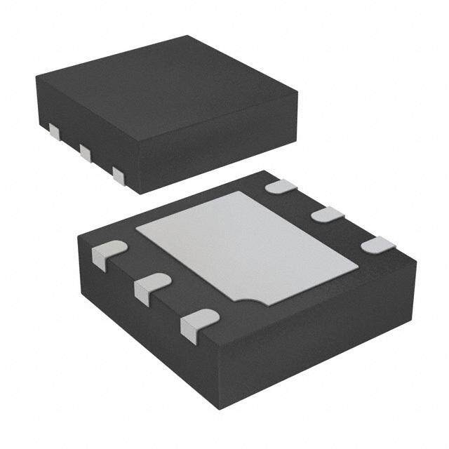
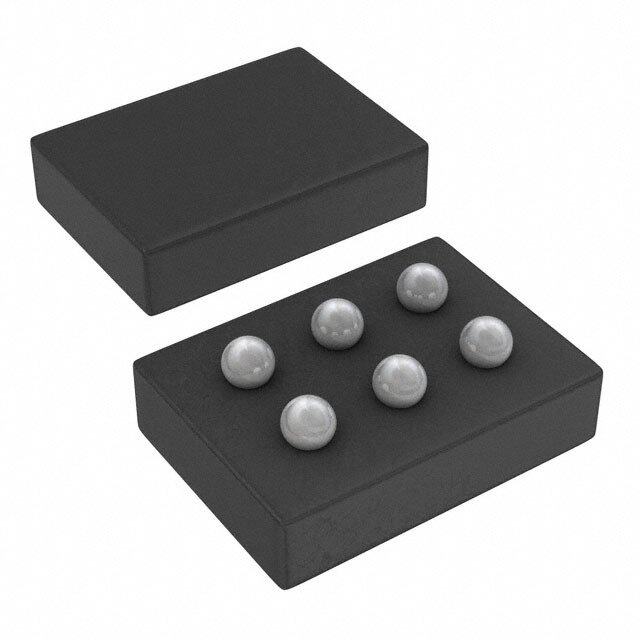
| 供应商器件封装 | 16-DSBGA(2x2) |
| 其它名称 | 296-29401-1 |
| 包装 | 剪切带 (CT) |
| 同步整流器 | 是 |
| 安装类型 | 表面贴装 |
| 封装/外壳 | 16-UFBGA,DSBGA |
| 工作温度 | -40°C ~ 85°C |
| 标准包装 | 1 |
| 电压-输入 | 2.5 V ~ 5.5 V |
| 电压-输出 | 0.77 V ~ 1.4 V |
| 电流-输出 | 2.5A |
| 类型 | 降压(降压) |
| 输出数 | 1 |
| 输出类型 | 可调式 |
| 配用 | /product-detail/zh/TPS62362EVM-655/TPS62362EVM-655-ND/2768994 |
| 频率-开关 | 2.5MHz |


PDF Datasheet 数据手册内容提取
TPS62360, TPS62361B TPS62362, TPS62363 www.ti.com SLVSAU9C–MAY2011–REVISEDNOVEMBER2012 2 3A Processor Supply with I C Compatible Interface and Remote Sense CheckforSamples:TPS62360,TPS62361B,TPS62362,TPS62363 FEATURES DESCRIPTION 1 • 3APeakOutputCurrent The TPS6236x are a family of high-frequency 2 synchronous step down dc-dc converter optimized for • HighestEfficiency: battery-powered portable applications for a small – LowRDS,on SwitchandActiveRectifier solution size. With an input voltage range of 2.5V to – PowerSaveModeforLightLoads 5.5V, common battery technologies are supported. The device provides up to 3A peak load current, • I2CHighSpeedCompatibleInterface operatingat2.5MHztypicalswitchingfrequency. • ProgrammableOutputVoltageforDigital The devices convert to an output voltage range of VoltageScaling 0.77V to 1.4V (TPS62360/62) and 0.5V to 1.77V – TPS62360/62:0.77Vto1.4V,10mVSteps (TPS62361B/63), programmable via I2C interface in – TPS62361B/63:0.5Vto1.77V,10mVSteps 10mV steps. Dedicated inputs allow fast voltage • ExcellentDC/ACOutputVoltageRegulation transition to address processor performance operatingpoints. – DifferentialLoadSensing The TPS6236x supports low-voltage DSPs and – PreciseDCOutputVoltageAccuracy processor cores in smart-phones and handheld – DCS-Control™ArchitectureforFastand computers including latest submicron processes. PreciseTransientRegulation Dedicated hardware input pins allow simple • MultipleRobustOperation/Protection transitions to performance operating points and Features: retentionmodesofprocessors. – SoftStart The devices focus on a high output voltage accuracy. – ProgrammableSlewRateatVoltage The differential sensing and the DCS-Control™ architecture achieve precise static and dynamic, Transition transientoutputvoltageregulation. – OverTemperatureProtection The TPS6236x devices offer high efficiency step – InputUnderVoltageDetectionandLockout down conversion. The area of highest efficiency is • Availablein16-Bump,2mmx2mm NanoFree™ extended towards low output currents to increase the Package efficiency while the processor is operating in retention • LowExternalDeviceCount: <25mm2Solution mode, as well as towards highest output currents Size increasingthebatteryon-time. The robust architecture and multiple safety features APPLICATIONS allowperfectsystemintegration. • DynamicVoltageScaleCompliantProcessors The 2mm x 2mm package and the low number of andDSPs,Memory required external components lead to a tiny solution • SmartReflex™CompliantPowerSupply sizeoflessthan25mm2. • CellPhones,SmartPhones,FeaturePhones 1mm • Tablets,Netbooks,Clamshells TPS6236x 2.5V .. 5.5V 0.47uH / 1µH VIN SW AVIN SW EN COUT 10µF 0.1µF SENSE+ LOAD VDD SENSE- SCL SDA 0.1µF PGND VSEL0 PGND VSEL1 AGND PGND 1 Pleasebeawarethatanimportantnoticeconcerningavailability,standardwarranty,anduseincriticalapplicationsof TexasInstrumentssemiconductorproductsanddisclaimerstheretoappearsattheendofthisdatasheet. DCS-Control,NanoFree,SmartReflexaretrademarksofTexasInstruments. 2 PRODUCTIONDATAinformationiscurrentasofpublicationdate. Copyright©2011–2012,TexasInstrumentsIncorporated Products conform to specifications per the terms of the Texas Instruments standard warranty. Production processing does not necessarilyincludetestingofallparameters.
TPS62360, TPS62361B TPS62362, TPS62363 SLVSAU9C–MAY2011–REVISEDNOVEMBER2012 www.ti.com Thesedeviceshavelimitedbuilt-inESDprotection.Theleadsshouldbeshortedtogetherorthedeviceplacedinconductivefoam duringstorageorhandlingtopreventelectrostaticdamagetotheMOSgates. ORDERINGINFORMATION PARTNUMBER PACKAGEMARKING PACKAGE DEVICESPECIFICFEATURES(1) OutputVoltageRange OutputVoltagePresets TPS62360(2) SeePACKAGE CSP-16 V =0.77Vto1.4V,10mVSteps 1.40V,1.00V,1.40V,1.10V OUT SUMMARYSection TPS62361B(2) SeePACKAGE CSP-16 V =0.5Vto1.77V,10mVSteps 0.96V,1.40V,1.16V,1.16V OUT SUMMARYSection TPS62362(2) SeePACKAGE CSP-16 V =0.77Vto1.4V,10mVSteps 1.23V,1.00V,1.20V,1.10V OUT SUMMARYSection TPS62363(2) SeePACKAGE CSP-16 V =0.5Vto1.77V,10mVSteps 1.20V,1.36V,1.50V,1.00V OUT SUMMARYSection (1) Contactthefactorytocheckavailabilityofotheroutputvoltageorfeatureversions. (2) TheYZHpackageisavailableintapeandreel.AddRsuffix(e.g.TPS62360YZHR)toorderquantitiesof3000partsperreel,Tsuffixfor 250partsperreel(e.g.TPS62360YZHT).Forthemostcurrentpackageandorderinginformation,seethePackageOptionAddendumat theendofthisdocument,orvisitthedeviceproductfolderonti.com. ABSOLUTE MAXIMUM RATINGS overoperatingfree-airtemperaturerange(unlessotherwisenoted)(1) VALUE UNIT MIN MAX VIN,AVIN,SWpin –0.3 7 V EN,VSEL0,VSEL1,SENSE+ –0.3 (V +0.3V) V AVIN Voltagerange(2) SENSE– –0.3 0.3 V SCL,SDA –0.3 (V +0.3V) V DD VDD –0.3 3.6 V ContinuousRMSVIN/SWcurrentperPin(3) 1275 mA Operatingjunctiontemperature,T –40 150 °C J Temperaturerange Storagetemperature,T –65 150 °C stg Machinemodel 200 V ESDrating(4) Chargedevicemodel 500 V Humanbodymodel 2 kV (1) Stressesbeyondthoselistedunderabsolutemaximumratingsmaycausepermanentdamagetothedevice.Thesearestressratings only,andfunctionaloperationofthedeviceattheseoranyotherconditionsbeyondthoseindicatedunderrecommendedoperating conditionsisnotimplied.Exposuretoabsolute–maximum–ratedconditionsforextendedperiodsmayaffectdevicereliability. (2) Allvoltagevaluesarewithrespecttonetworkgroundterminal. (3) InordertobeconsistentwiththeTIreliabilityrequirementforthesiliconchips(100KPower-On-Hoursat105°Cjunctiontemperature), thecurrentshouldnotcontinuouslyexceed1275mAintheVINpinand2550mAintheSWpinssoastopreventelectromigrationfailure inthesolder.SeeTHERMALANDDEVICELIFETIMEINFORMATION. (4) Thehumanbodymodelisa100-pFcapacitordischargedthrougha1.5-kΩresistorintoeachpin.Themachinemodelisa200-pF capacitordischargeddirectlyintoeachpin. 2 SubmitDocumentationFeedback Copyright©2011–2012,TexasInstrumentsIncorporated ProductFolderLinks:TPS62360 TPS62361BTPS62362 TPS62363
TPS62360, TPS62361B TPS62362, TPS62363 www.ti.com SLVSAU9C–MAY2011–REVISEDNOVEMBER2012 THERMAL INFORMATION TPS6236x THERMALMETRIC(1) YZH UNITS 16PINS θ Junction-to-ambientthermalresistance(2) 94.8 JA θ Junction-to-case(top)thermalresistance(3) 25 JCtop θ Junction-to-boardthermalresistance(4) 60 JB °C/W ψ Junction-to-topcharacterizationparameter(5) 3.2 JT ψ Junction-to-boardcharacterizationparameter(6) 57 JB θ Junction-to-case(bottom)thermalresistance(7) n/a JCbot (1) Formoreinformationabouttraditionalandnewthermalmetrics,seetheICPackageThermalMetricsapplicationreport,SPRA953. (2) Thejunction-to-ambientthermalresistanceundernaturalconvectionisobtainedinasimulationonaJEDEC-standard,high-Kboard,as specifiedinJESD51-7,inanenvironmentdescribedinJESD51-2a. (3) Thejunction-to-case(top)thermalresistanceisobtainedbysimulatingacoldplatetestonthepackagetop.NospecificJEDEC- standardtestexists,butaclosedescriptioncanbefoundintheANSISEMIstandardG30-88. (4) Thejunction-to-boardthermalresistanceisobtainedbysimulatinginanenvironmentwitharingcoldplatefixturetocontrolthePCB temperature,asdescribedinJESD51-8. (5) Thejunction-to-topcharacterizationparameter,ψ ,estimatesthejunctiontemperatureofadeviceinarealsystemandisextracted JT fromthesimulationdataforobtainingθ ,usingaproceduredescribedinJESD51-2a(sections6and7). JA (6) Thejunction-to-boardcharacterizationparameter,ψ ,estimatesthejunctiontemperatureofadeviceinarealsystemandisextracted JB fromthesimulationdataforobtainingθ ,usingaproceduredescribedinJESD51-2a(sections6and7). JA (7) Thejunction-to-case(bottom)thermalresistanceisobtainedbysimulatingacoldplatetestontheexposed(power)pad.Nospecific JEDECstandardtestexists,butaclosedescriptioncanbefoundintheANSISEMIstandardG30-88. Spacer RECOMMENDED OPERATING CONDITIONS MIN TYP MAX UNIT V Inputvoltagerange,V I ≤2.5A 2.5 5.5 V IN IN OUT I >2.5A 3 5.5 V OUT I Continuousoutputcurrent(1) 2.5 A OUT,avg t RisingandfallingsignaltransitiontimeatEN,VSELx 30 mV/µs rf T Operatingambienttemperature(2) –40 85 °C A T Operatingjunctiontemperature –40 125 °C J (1) TheTPS6236xdeviceisdesignedtoprovide3Aaccordingtotypicalapplicationprocessorloadprofiles.Drawingmorethan2.5A permanentlymightimpactthedevicelifetime.SeeTHERMALANDDEVICELIFETIMEINFORMATIONfordetails. (2) Inapplicationswherehighpowerdissipationand/orpoorpackagethermalresistanceispresent,themaximumambienttemperaturemay havetobederated.Maximumambienttemperature[T ]isdependentonthemaximumoperatingjunctiontemperature[T ],the A(max) J(max) maximumpowerdissipationofthedeviceintheapplication[P ],andthejunction-to-ambientthermalresistanceofthepart/package D(max) intheapplication(θ ),asgivenbythefollowingequation:T =T –(θ ×P ) JA A(max) J(max) JA D(max) ELECTRICAL CHARACTERISTICS UnlessotherwisenotedthespecificationappliesforVIN=3.6Voveranoperatingambienttemp.–40°C≤T ≤85°C;Circuit A ofParameterMeasurementInformationsection(unlessotherwisenoted).TypicalvaluesareforT =25°C. A PARAMETER TESTCONDITIONS MIN TYP MAX UNIT INPUT V InputvoltagerangeatVIN,AVIN 2.5 5.5 V IN V I2Candregisterssupplyvoltagerange 1.15 3.6 V DD I ShutdowncurrentintoAVIN EN=LOW,V =0V 0.65 5 µA SD(AVIN) DD EN=LOW, TA=25°C 0.5 1 µA I ShutdowncurrentintoVIN SD(VIN) VDD=0V TA=85°C 1 3 µA I ShutdowncurrentintoVDD EN=LOW,I2Cbusidle 0.01 µA SD(VDD) Copyright©2011–2012,TexasInstrumentsIncorporated SubmitDocumentationFeedback 3 ProductFolderLinks:TPS62360 TPS62361BTPS62362 TPS62363
TPS62360, TPS62361B TPS62362, TPS62363 SLVSAU9C–MAY2011–REVISEDNOVEMBER2012 www.ti.com ELECTRICAL CHARACTERISTICS (continued) UnlessotherwisenotedthespecificationappliesforVIN=3.6Voveranoperatingambienttemp.–40°C≤T ≤85°C;Circuit A ofParameterMeasurementInformationsection(unlessotherwisenoted).TypicalvaluesareforT =25°C. A PARAMETER TESTCONDITIONS MIN TYP MAX UNIT PFMmode 56 µA EN=HIGH, I Operatingquiescentcurrentinto(AVIN I =0mA, ForcedPWM Q +VIN) nOoUtTswitching mode 180 µA (TestMode) Inputvoltagefalling,EN=High 2.3 2.45 V V UndervoltagelockoutatAVIN UVLO Inputvoltagerising,EN=Low 1.3 V Undervoltagelockouthysteresisat V Inputvoltagerising 110 mV UVLO,HYST(AVIN) AVIN V UndervoltagelockoutatVDD Inputvoltagefalling 0.7 0.92 1.1 V DD,UVLO Undervoltagelockouthysteresisat V Inputvoltagerising 50 mV UVLO,HYST(VDD) VDD I2Cnotactive 0 µA I InputcurrentatVDD VDD I2Cactive(r/w) 0.02 1 mA LOGICINTERFACE High-levelinputvoltageatEN,VSEL0, V 1.2 V IH VSEL1 Low-levelinputvoltageatEN,VSEL0, V 0.4 V IL VSEL1 V High-levelinputvoltageatSCL,SDA 0.7xV V IH,I2C DD V Low-levelinputvoltageatSCL,SDA 0.3xV V IL,I2C DD LogicinputleakagecurrentatEN, Internalpulldownresistors I 0.05 µA LKG VSEL0,VSEL1,SDA,SCL disabled PulldownresistanceatEN,VSEL0, Internalpulldownresistors R 300 kΩ PD VSEL1 enabled Fastmode 400 kHz I2Cclockfrequency Highspeedmode 3.4 MHz POWERSWITCH HighsideMOSFETswitch V =3.6V 25 44 75 mΩ IN R DS(on) LowsideMOSFETswitch V =3.6V 25 32 50 mΩ IN HighsideMOSFETforwardcurrentlimit V =3.6V 3.0 3.6 4.3 A IN LowsideMOSFETforwardcurrentlimit V =3.6V 2.6 3 3.8 A I IN LIMF LowsideMOSFETnegativecurrent V =3.6V,PWMmode 2.2 2.5 2.9 A limit IN f Nominalswitchingfrequency PWMmode 2.5 MHz SW T Dietemperatureearlywarning 120 °C JEW T Thermalshutdown 150 °C JSD T Thermalshutdownhysteresis 20 °C JSD,HYST t Minimumontime 120 ns ON,min OUTPUT 10mV TPS62360/62 0.77 1.4 V Outputvoltagerange V OUT increments TPS62361B/63 0.5 1.77 TPS62360/62: Noload,Forced V =2.5V.. PWM, IN 5.5V V =[0.77V, -0.5% +0.5% OUT V =0.77V.. 1.3V] OUT 1.4V T =85°C J Outputvoltageaccuracy TPS62361B/63: Noload,Forced V =2.7V.. IN PWM, 5.5V -1% ±0.5% +1% T =-40.. V =0.5V.. J OUT 150°C 1.77V 4 SubmitDocumentationFeedback Copyright©2011–2012,TexasInstrumentsIncorporated ProductFolderLinks:TPS62360 TPS62361BTPS62362 TPS62363
TPS62360, TPS62361B TPS62362, TPS62363 www.ti.com SLVSAU9C–MAY2011–REVISEDNOVEMBER2012 ELECTRICAL CHARACTERISTICS (continued) UnlessotherwisenotedthespecificationappliesforVIN=3.6Voveranoperatingambienttemp.–40°C≤T ≤85°C;Circuit A ofParameterMeasurementInformationsection(unlessotherwisenoted).TypicalvaluesareforT =25°C. A PARAMETER TESTCONDITIONS MIN TYP MAX UNIT Lineregulation I =1A,forcedPWM <0.1 %/V OUT Loadregulation V =1.2V,forcedPWM <0.05 %/A OUT TimefromactiveENto V =1.4V, t Start-uptime OUT 1 ms Start C <100µF,RMP[2:0]=000, OUT I =0mA OUT InputresistancebetweenSense+, R 2.2 MΩ Sense Sense– RMP[2:0]=000 32 RMP[2:0]=001 16 RMP[2:0]=010 8 RMP[2:0]=011 4 Ramptimer mV/µs RMP[2:0]=100 2 RMP[2:0]=101 1 RMP[2:0]=110 0.5 RMP[2:0]=111 0.25 Copyright©2011–2012,TexasInstrumentsIncorporated SubmitDocumentationFeedback 5 ProductFolderLinks:TPS62360 TPS62361BTPS62362 TPS62363
TPS62360, TPS62361B TPS62362, TPS62363 SLVSAU9C–MAY2011–REVISEDNOVEMBER2012 www.ti.com I2C INTERFACE TIMING REQUIREMENTS(1)(2) PARAMETER TESTCONDITIONS MIN MAX UNIT Standardmode 100 kHz Fastmode 400 kHz High-speedmode(writeoperation),C –100pF B 3.4 MHz max f(SCL) SCLclockfrequency High-speedmode(readoperation),CB–100pF 3.4 MHz max High-speedmode(writeoperation),C –400pF B 1.7 MHz max High-speedmode(readoperation),C –400pF B 1.7 MHz max BusfreetimebetweenaSTOPand Standardmode 4.7 μs t BUF STARTcondition Fastmode 1.3 μs Standardmode 4 μs t ,t Holdtime(repeated)STARTcondition Fastmode 600 ns HD STA High-speedmode 160 ns Standardmode 4.7 μs Fastmode 1.3 μs t LowperiodoftheSCLclock LOW High-speedmode,C –100pFmax 160 ns B High-speedmode,C –400pFmax 320 ns B Standardmode 4 μs Fastmode 600 ns t HighperiodoftheSCLclock HIGH High-speedmode,C –100pFmax 60 ns B High-speedmode,C –400pFmax 120 ns B Standardmode 4.7 μs SetuptimeforarepeatedSTART t ,t Fastmode 600 ns SU STA condition High-speedmode 160 ns Standardmode 250 ns t ,t Datasetuptime Fastmode 100 ns SU DAT High-speedmode 10 ns Standardmode 0 3.45 μs Fastmode 0 0.9 μs t ,t Dataholdtime HD DAT High-speedmode,C –100pFmax 0 70 ns B High-speedmode,C –400pFmax 0 150 ns B Standardmode 20+0.1C 1000 ns B Fastmode 20+0.1C 300 ns B t RisetimeofSCLsignal RCL High-speedmode,C –100pFmax 10 40 ns B High-speedmode,C –400pFmax 20 80 ns B Standardmode 20+0.1C 1000 ns B RisetimeofSCLsignalafterarepeated Fastmode 20+0.1C 300 ns B t STARTconditionandafteran RCL1 acknowledgebit High-speedmode,CB–100pFmax 10 80 ns High-speedmode,C –400pFmax 20 160 ns B Standardmode 20+0.1C 300 ns B Fastmode 20+0.1C 300 ns B t FalltimeofSCLsignal FCL High-speedmode,C –100pFmax 10 40 ns B High-speedmode,C –400pFmax 20 80 ns B (1) S/M=standardmode;F/M=fastmode (2) Specifiedbydesign.Nottestedinproduction. 6 SubmitDocumentationFeedback Copyright©2011–2012,TexasInstrumentsIncorporated ProductFolderLinks:TPS62360 TPS62361BTPS62362 TPS62363
TPS62360, TPS62361B TPS62362, TPS62363 www.ti.com SLVSAU9C–MAY2011–REVISEDNOVEMBER2012 I2C INTERFACE TIMING REQUIREMENTS(1)(2) (continued) PARAMETER TESTCONDITIONS MIN MAX UNIT Standardmode 20+0.1C 1000 ns B Fastmode 20+0.1C 300 ns B t RisetimeofSDAsignal RDA High-speedmode,C –100pFmax 10 80 ns B High-speedmode,C –400pFmax 20 160 ns B Standardmode 20+0.1C 300 ns B Fastmode 20+0.1C 300 ns B t FalltimeofSDAsignal FDA High-speedmode,C –100pFmax 10 80 ns B High-speedmode,C –400pFmax 20 160 ns B Standardmode 4 μs t ,t SetuptimeforSTOPcondition Fastmode 600 ns SU STO High-speedmode 160 ns C CapacitiveloadforSDAandSCL 400 pF B I2C TIMING DIAGRAMS SDA t tf t t su;DAT t thd;STA thd;STA tr tBUF LOW r f SCL t t t hd;STA hd;DAT su;STO HIGH S Sr P S Figure1. SerialInterfaceTimingforF/SMode Sr P t t fDA rDA SDAH t hd;DAT t t t t su;STA hd;STA su;DAT su;STO SCLH Sr t t fCL t t fCL1 fCL rCL1 t t t t See NoteA HIGH LOW LOW HIGH See NoteA = MCS Current Source Pull-Up = R(P)Resistor Pull-Up NoteA: First rising edge of the SCLH signal after Sr and after each acknowledge bit. Figure2. SerialInterfaceTimingforH/SMode Copyright©2011–2012,TexasInstrumentsIncorporated SubmitDocumentationFeedback 7 ProductFolderLinks:TPS62360 TPS62361BTPS62362 TPS62363
TPS62360, TPS62361B TPS62362, TPS62363 SLVSAU9C–MAY2011–REVISEDNOVEMBER2012 www.ti.com DEVICE INFORMATION PIN ASSIGNMENTS (TOP VIEW) (BOTTOM VIEW) AVIN AGND VSEL1 VIN A1 A2 A3 A4 A4 A3 A2 A1 SENSE+ EN SW SW B1 B2 B3 B4 B4 B3 B2 B1 SENSE- VSEL0 PGND PGND C1 C2 C3 C4 C4 C3 C2 C1 VDD SDA SCL PGND D1 D2 D3 D4 D4 D3 D2 D1 PINFUNCTIONS PIN I/O DESCRIPTION NAME NO. AVIN A1 I AnalogSupplyVoltageInput. AGND A2 – AnalogGroundConnection. EN B2 I DeviceEnableLogicInput.LogicHIGHenablesthedevice,logicLOWdisablesthedeviceandturnsitinto shutdown.ThepinmustbeterminatedtoeitherHIGHorLOWiftheinternalpulldownresistorisdeactivated. VDD D1 I I2CLogicandRegisterssupplyvoltage.Forresettingtheinternalregisters,thisconnectionmustbepulledbelow itsUVLOlevel. SCL D3 I/O I2Cclocksignal. SDA D2 I/O I2Cdatasignal. VSEL0 C2 I OutputSettingsSelectionLogicInputs.Predefinedregistersettingscanbechosenforsettingoutputvoltageand VSEL1 A3 I mode.ThepinsmustbeterminatedtologicHIGHorLOWiftheinternalpulldownresistorsaredeactivated. B3 – SW Inductorconnection B4 SENSE+ B1 I PositiveOutputVoltageRemoteSense.Mustbeconnectedclosesttotheloadsupplynode. SENSE– C1 I NegativeOutputVoltageRemoteSense.Mustbeconnectedclosesttotheloadgroundnode. VIN A4 I PowerSupplyVoltageInput. C3 – PGND C4 PowerGroundConnection. D4 8 SubmitDocumentationFeedback Copyright©2011–2012,TexasInstrumentsIncorporated ProductFolderLinks:TPS62360 TPS62361BTPS62362 TPS62363
TPS62360, TPS62361B TPS62362, TPS62363 www.ti.com SLVSAU9C–MAY2011–REVISEDNOVEMBER2012 FUNCTIONAL BLOCK DIAGRAM ramp direct control & compensation Softstart comparator error DifSfeernesnetial SENSE+ AVIN amplifier Analog SENSE- AGND Circuit Supply Thermal Shutdown DCS-CONTROLTM REF EN RDIS- CHARGE VDD I2C High Side SCL Interface Current Limit SDA VIN Bandgap CLoongtricol DGriavteer HPig-hM SOiSde SW2 Under Voltage Shutdown LNow-M SOidSe PGND3 VSEL0 Low Side VSEL1 Current Limit Copyright©2011–2012,TexasInstrumentsIncorporated SubmitDocumentationFeedback 9 ProductFolderLinks:TPS62360 TPS62361BTPS62362 TPS62363
TPS62360, TPS62361B TPS62362, TPS62363 SLVSAU9C–MAY2011–REVISEDNOVEMBER2012 www.ti.com TYPICAL CHARACTERISTICS TableofGraphs FIGURE V =1.5V Figure3 OUT V =1.4V Figure4 OUT V =1.2V Figure5 OUT vs.OutputCurrent(PowerSaveandForced V =1.1V Figure6 PWMMode) OUT V =1.0V Figure7 OUT η Efficiency V =0.9V Figure8 OUT V =0.6V Figure9 OUT I =3000mA Figure10 OUT vs.InputVoltage(PowerSaveandForcedPWM IOUT=1000mA Figure11 Mode) I =100mA Figure12 OUT I =10mA Figure13 OUT V =1.5V,T = OUT A Figure14 25°C V =1.2V,T = OUT A Figure15 vs.OutputCurrent(PowerSaveandForced 25°C V DCOutputVoltage O PWMMode) V =0.9V,T = OUT A Figure16 25°C V =0.6V,T = OUT A Figure17 25°C V =0.5V,I = OUT OUT Figure18 0mA IntoNoLoad V =1.5V,I = OUT OUT Figure19 0mA Startup V =0.5V,I = OUT OUT Figure20 1000mA IntoLoad V =1.5V,I = OUT OUT Figure21 1000mA I =10mA Figure22 OUT I =200mA Figure23 OUT SwitchingWaveforms I =1000mA Figure24 OUT I =3000mA Figure25 OUT I =0mA Figure26 OUT OutputVoltageRampControl Transition0.6V..1.5V I =1000mA Figure27 OUT I =5mAto200mA Figure28 OUT I =5mAto1000mA Figure29 OUT LoadTransientResponse IOUT=200mAto Figure30 1000mA I =1000mAto OUT Figure31 3000mA LineTransientResponse V =3.2to4.2V Figure32 IN I , ShutdownCurrentatAVINand T =[-40°C,25°C, SD(VIN) vs.InputVoltage A Figure33 I VIN 125°C] SD(AVIN) T =[-40°C,25°C, A 125°C], Figure34 autoPFM/PWM I QuiescentCurrent vs.InputVoltage Q T =[-40°C,25°C, A 125°C] Figure35 forcedPWM f SwitchingFrequency vs.OutputCurrent V =1.2V Figure36 SW OUT I CurrentLimit vs.InputVoltage Figure37 LIM 10 SubmitDocumentationFeedback Copyright©2011–2012,TexasInstrumentsIncorporated ProductFolderLinks:TPS62360 TPS62361BTPS62362 TPS62363
TPS62360, TPS62361B TPS62362, TPS62363 www.ti.com SLVSAU9C–MAY2011–REVISEDNOVEMBER2012 TYPICAL CHARACTERISTICS (continued) EFFICIENCY EFFICIENCY vs vs OUTPUTCURRENT OUTPUTCURRENT V =1.5V V =1.4V OUT OUT 100 100 90 90 80 80 70 70 %) 60 %) 60 ncy ( 50 TVPOUST6 =2 316.51VB ncy ( 50 TVPOUST6 =2 316.4xV cie TA = 25°C cie TA = 25°C Effi 40 Effi 40 30 30 Forced PWM, VIN = 2.8V Forced PWM, VIN = 2.8V 20 Forced PWM, VIN = 3.6V 20 Forced PWM, VIN = 3.6V Forced PWM, VIN = 4.2V Forced PWM, VIN = 4.2V Auto PFM/PWM, VIN = 2.8V Auto PFM/PWM, VIN = 2.8V 10 Auto PFM/PWM, VIN = 3.6V 10 Auto PFM/PWM, VIN = 3.6V Auto PFM/PWM, VIN = 4.2V Auto PFM/PWM, VIN = 4.2V 0 0 1m 10m 100m 1 3 1m 10m 100m 1 3 Output Current (A) Output Current (A) G001 G002 Figure3. Figure4. EFFICIENCY EFFICIENCY vs vs OUTPUTCURRENT OUTPUTCURRENT V =1.2V V =1.1V OUT OUT 100 100 90 90 80 80 70 70 %) 60 %) 60 ncy ( 50 TVPOUST6 =2 316.2xV ncy ( 50 TVPOUST6 =2 316.1xV cie TA = 25°C cie TA = 25°C Effi 40 Effi 40 30 30 Forced PWM, VIN = 2.8V Forced PWM, VIN = 2.8V 20 Forced PWM, VIN = 3.6V 20 Forced PWM, VIN = 3.6V Forced PWM, VIN = 4.2V Forced PWM, VIN = 4.2V Auto PFM/PWM, VIN = 2.8V Auto PFM/PWM, VIN = 2.8V 10 Auto PFM/PWM, VIN = 3.6V 10 Auto PFM/PWM, VIN = 3.6V Auto PFM/PWM, VIN = 4.2V Auto PFM/PWM, VIN = 4.2V 0 0 1m 10m 100m 1 3 1m 10m 100m 1 3 Output Current (A) Output Current (A) G003 G004 Figure5. Figure6. Copyright©2011–2012,TexasInstrumentsIncorporated SubmitDocumentationFeedback 11 ProductFolderLinks:TPS62360 TPS62361BTPS62362 TPS62363
TPS62360, TPS62361B TPS62362, TPS62363 SLVSAU9C–MAY2011–REVISEDNOVEMBER2012 www.ti.com TYPICAL CHARACTERISTICS (continued) EFFICIENCY EFFICIENCY vs vs OUTPUTCURRENT OUTPUTCURRENT V =1.0V V =0.9V OUT OUT 100 100 90 90 80 80 70 70 %) 60 %) 60 ncy ( 50 TVPOUST6 =2 316.0xV ncy ( 50 TVPOUST6 =2 306.9xV cie TA = 25°C cie TA = 25°C Effi 40 Effi 40 30 30 Forced PWM, VIN = 2.8V Forced PWM, VIN = 2.8V 20 Forced PWM, VIN = 3.6V 20 Forced PWM, VIN = 3.6V Forced PWM, VIN = 4.2V Forced PWM, VIN = 4.2V Auto PFM/PWM, VIN = 2.8V Auto PFM/PWM, VIN = 2.8V 10 Auto PFM/PWM, VIN = 3.6V 10 Auto PFM/PWM, VIN = 3.6V Auto PFM/PWM, VIN = 4.2V Auto PFM/PWM, VIN = 4.2V 0 0 1m 10m 100m 1 3 1m 10m 100m 1 3 Output Current (A) Output Current (A) G005 G006 Figure7. Figure8. EFFICIENCY EFFICIENCY vs vs OUTPUTCURRENT INPUTVOLTAGE V =0.6V I =3A OUT OUT 100 100 90 90 80 80 70 70 %) 60 %) 60 ncy ( 50 TVPOUST6 =2 306.61VB ncy ( 50 cie TA = 25°C cie Effi 40 Effi 40 30 30 Forced PWM, VIN = 2.8V 20 Forced PWM, VIN = 3.6V 20 Forced PWM, VIN = 4.2V Auto PFM/PWM, VIN = 2.8V TPS6236x Auto PFM/PWM, VOUT = 1.0V 10 Auto PFM/PWM, VIN = 3.6V 10 IOUT = 3A Auto PFM/PWM, VOUT = 1.1V Auto PFM/PWM, VIN = 4.2V TA = 25°C Auto PFM/PWM, VOUT = 1.4V 0 0 1m 10m 100m 1 3 2.5 3.0 3.5 4.0 4.5 5.0 5.5 Output Current (A) Input Voltage (V) G007 G008 Figure9. Figure10. 12 SubmitDocumentationFeedback Copyright©2011–2012,TexasInstrumentsIncorporated ProductFolderLinks:TPS62360 TPS62361BTPS62362 TPS62363
TPS62360, TPS62361B TPS62362, TPS62363 www.ti.com SLVSAU9C–MAY2011–REVISEDNOVEMBER2012 TYPICAL CHARACTERISTICS (continued) EFFICIENCY EFFICIENCY vs vs INPUTVOLTAGE INPUTVOLTAGE I =1A I =100mA OUT OUT 100 100 90 90 80 80 70 70 %) 60 %) 60 y ( y ( nc 50 nc 50 e e ci ci Effi 40 Effi 40 30 30 Forced PWM, VOUT = 1.0V 20 20 Forced PWM, VOUT = 1.1V Forced PWM, VOUT = 1.4V TPS6236x Auto PFM/PWM, VOUT = 1.0V TPS6236x Auto PFM/PWM, VOUT = 1.0V 10 IOUT = 1A Auto PFM/PWM, VOUT = 1.1V 10 IOUT = 100mA Auto PFM/PWM, VOUT = 1.1V TA = 25°C Auto PFM/PWM, VOUT = 1.4V TA = 25°C Auto PFM/PWM, VOUT = 1.4V 0 0 2.5 3.0 3.5 4.0 4.5 5.0 5.5 2.5 3.0 3.5 4.0 4.5 5.0 5.5 Input Voltage (V) Input Voltage (V) G009 G010 Figure11. Figure12. EFFICIENCY DCOUTPUTVOLTAGE vs vs INPUTVOLTAGE OUTPUTCURRENT I =10mA V =1.5V OUT OUT 100 1.55 TPS62361B 90 1.54 VOUT = 1.5V TA = 25°C 80 1.53 70 1.52 Efficiency (%) 456000 FFFAAAooouuurrrtttcccoooeee PPPdddFFF PPPMMMWWW///PPPMMMWWW,,, MMMVVVOOO,,, UUUVVVTTTOOO ===UUU TTT111 ===...014 111VVV...014VVV Output Voltage (V) 111...455901 C D 30 1.48 Forced PWM, VIN = 2.8V 20 1.47 Forced PWM, VIN = 3.6V Forced PWM, VIN = 4.2V TPS6236x Auto PFM/PWM, VIN = 2.8V 10 IOUT = 10mA 1.46 Auto PFM/PWM, VIN = 3.6V TA = 25°C Auto PFM/PWM, VIN = 4.2V 0 1.45 2.5 3.0 3.5 4.0 4.5 5.0 5.5 1m 10m 100m 1 3 Input Voltage (V) Output Current (A) G011 G012 Figure13. Figure14. Copyright©2011–2012,TexasInstrumentsIncorporated SubmitDocumentationFeedback 13 ProductFolderLinks:TPS62360 TPS62361BTPS62362 TPS62363
TPS62360, TPS62361B TPS62362, TPS62363 SLVSAU9C–MAY2011–REVISEDNOVEMBER2012 www.ti.com TYPICAL CHARACTERISTICS (continued) DCOUTPUTVOLTAGE DCOUTPUTVOLTAGE vs vs OUTPUTCURRENT OUTPUTCURRENT V =1.2V V =0.9V OUT OUT 1.25 0.95 TPS6236x TPS6236x 1.24 VOUT = 1.2V 0.94 VOUT = 0.9V TA = 25°C TA = 25°C 1.23 0.93 1.22 0.92 V) V) ge ( 1.21 ge ( 0.91 a a olt olt V 1.20 V 0.90 ut ut p p Out 1.19 Out 0.89 C C D D 1.18 0.88 Forced PWM, VIN = 2.8V Forced PWM, VIN = 2.8V 1.17 Forced PWM, VIN = 3.6V 0.87 Forced PWM, VIN = 3.6V Forced PWM, VIN = 4.2V Forced PWM, VIN = 4.2V Auto PFM/PWM, VIN = 2.8V Auto PFM/PWM, VIN = 2.8V 1.16 Auto PFM/PWM, VIN = 3.6V 0.86 Auto PFM/PWM, VIN = 3.6V Auto PFM/PWM, VIN = 4.2V Auto PFM/PWM, VIN = 4.2V 1.15 0.85 1m 10m 100m 1 3 1m 10m 100m 1 3 Output Current (A) Output Current (A) G013 G014 Figure15. Figure16. DCOUTPUTVOLTAGE vs OUTPUTCURRENT STARTUPINTONOLOAD V =0.6V V =0.5V OUT OUT 0.65 TPS62361B TPS62361B RAMP[2:0] = 000 (32mV/μs) 0.64 VTAO U=T 2=5 0°C.6V IVOUT== 3 0.6AV VOUT200mV/Div IN 0.63 VOUT= 0.5V 0.62 V) ge ( 0.61 a olt V 0.60 ut p Out 0.59 C D Inductor Current 200mA/Div 0.58 Forced PWM, VIN = 2.8V 0.57 Forced PWM, VIN = 3.6V EN 2V/DIV Forced PWM, VIN = 4.2V Auto PFM/PWM, VIN = 2.8V 0.56 Auto PFM/PWM, VIN = 3.6V Auto PFM/PWM, VIN = 4.2V 0.55 1m 10m 100m 1 3 Time Base - 20μs/Div Output Current (A) G015 G017 Figure17. Figure18. 14 SubmitDocumentationFeedback Copyright©2011–2012,TexasInstrumentsIncorporated ProductFolderLinks:TPS62360 TPS62361BTPS62362 TPS62363
TPS62360, TPS62361B TPS62362, TPS62363 www.ti.com SLVSAU9C–MAY2011–REVISEDNOVEMBER2012 TYPICAL CHARACTERISTICS (continued) STARTUPINTONOLOAD STARTUPINTOLOAD V =1.5V V =0.5V OUT OUT TPS62361B TPS62361B RAMP[2:0] = 000 (32mV/μs) RAMP[2:0] = 000 (32mV/μs) I = 0A I = 1A OUT V 1V/Div OUT V 200mV/Div V = 3.6V OUT V = 3.6V OUT IN IN V = 1.5V V = 0.5V OUT OUT Inductor Current 500mA/Div Inductor Current 500mA/Div EN 2V/DIV EN 2V/DIV Time Base - 20μs/Div Time Base - 20μs/Div G018 G019 Figure19. Figure20. STARTUPINTOLOAD SWITCHINGWAVEFORMS V =1.5V I =10mA OUT OUT TPS62361B RAMP[2:0] = 000 (32mV/μs) I = 1A LOAD V = 3.6V IN V = 1.5V OUT VOUT1V/Div VOUT10mV/Div w/ 1.2V Offset Inductor Current 200mA/Div Inductor Current 1A/Div EN 2V/DIV SW Pin 2V/Div TPS62361B V = 3.6V IN IOUT= 10mA VOUT= 1.2V Time Base - 20μs/Div Time Base - 4μs/Div G020 G021 Figure21. Figure22. Copyright©2011–2012,TexasInstrumentsIncorporated SubmitDocumentationFeedback 15 ProductFolderLinks:TPS62360 TPS62361BTPS62362 TPS62363
TPS62360, TPS62361B TPS62362, TPS62363 SLVSAU9C–MAY2011–REVISEDNOVEMBER2012 www.ti.com TYPICAL CHARACTERISTICS (continued) SWITCHINGWAVEFORMS SWITCHINGWAVEFORMS I =200mA I =1A OUT OUT TPS62361B TPS62361B I = 200mA I = 1A OUT OUT V = 3.6V V = 3.6V IN IN VOUT= 1.2V VOUT10mV/Div w/ 1.2V Offset VOUT= 1.2V VOUT10mV/Div w/ 1.2V Offset Inductor Current 200mA/Div w/ 200mAOffset Inductor Current 200mA/Div w/ 1AOffset SW Pin 2V/Div SW Pin 2V/Div Time Base - 250ns/Div Time Base - 250ns/Div G022 G023 Figure23. Figure24. SWITCHINGWAVEFORMS OUTPUTVOLTAGERAMPCONTROL I =3A NOLOAD OUT TPS62361B TPS62361B IOUT= 3A RAMP[2:0] = 000 (32mV/μs) VOUT1V/Div w/ 0.6V Offset V = 3.6V IN V = 1.2V OUT V 10mV/Div w/ 1.2V Offset OUT Inductor Current 200mA/Div w/ 3AOffset I = 0A OUT V = 3.6V IN V = 0.6V to 1.5V OUT Inductor Current 500mA/Div V 2V/Div SEL0 SW Pin 2V/Div Time Base - 250ns/Div Time Base - 20μs/Div G024 G025 Figure25. Figure26. 16 SubmitDocumentationFeedback Copyright©2011–2012,TexasInstrumentsIncorporated ProductFolderLinks:TPS62360 TPS62361BTPS62362 TPS62363
TPS62360, TPS62361B TPS62362, TPS62363 www.ti.com SLVSAU9C–MAY2011–REVISEDNOVEMBER2012 TYPICAL CHARACTERISTICS (continued) OUTPUTVOLTAGERAMPCONTROL LOADTRANSIENTRESPONSE I =1A I RANGE:5mAto200mA OUT OUT TPS62361B TPS62361B V = 3.6V IN RAMP[2:0] = 000 (32mV/μs) VOUT1V/Div w/ 0.6V Offset CLOAD= 22μF VOUT= 1.2V V 20mV/Div w/ 1.2V Offset OUT Inductor Current 500mA/Div I = 1A OUT Inductor Current 200mA/Div V = 3.6V IN V = 0.6V to 1.5V OUT V 2V/Div SEL0 I 100mA/Div OUT Time Base - 20μs/Div Time Base - 100μs/Div G026 G027 Figure27. Figure28. LOADTRANSIENTRESPONSE LOADTRANSIENTRESPONSE I RANGE:5mAto1A I RANGE:200mAto1A OUT OUT TPS62361B TPS62361B C = 22μF C = 22μF LOAD LOAD V = 3.6V V = 3.6V IN IN V = 1.2V V = 1.2V OUT OUT V 50mV/Div w/ 1.2V Offset V 50mV/Div w/ 1.2V Offset OUT OUT Inductor Current 500mA/Div Inductor Current 500mA/Div I 1A/Div I 1A/Div OUT OUT Time Base - 100μs/Div Time Base - 100μs/Div G028 G029 Figure29. Figure30. Copyright©2011–2012,TexasInstrumentsIncorporated SubmitDocumentationFeedback 17 ProductFolderLinks:TPS62360 TPS62361BTPS62362 TPS62363
TPS62360, TPS62361B TPS62362, TPS62363 SLVSAU9C–MAY2011–REVISEDNOVEMBER2012 www.ti.com TYPICAL CHARACTERISTICS (continued) LOADTRANSIENTRESPONSE LINETRANSIENTRESPONSE I RANGE:1Ato3A V RANGE:4.2Vto3.2V OUT IN TPS62361B TPS62361B VOUT= 1.2V CLOAD= 22μF CLOAD= 22μF CIN= 100nF IOUT= 300mA V = 3.6V IN V = 1.2V OUT V 1V/Div w/ 4.2V Offset IN V 50mV/Div w/ 1.2V Offset OUT V 20mV/Div w/ 1.2V Offset OUT Inductor Current 1A/Div Inductor Current 200mA/Div I 2A/Div OUT Time Base - 100μs/Div Time Base - 20μs/Div G030 G031 Figure31. Figure32. SHUTDOWNCURRENT QUIESCENTCURRENT vs vs INPUTVOLTAGE INPUTVOLTAGE 10 150 TPS6236x MODE0 = 0 (Auto PFM/PWM) 130 EN = HIGH 1 110 A) A) µ µ ent ( ent ( 90 Curr 0.1 TPS6236x Curr wn EN = LOW ent 70 o c d s hut uie S Q 50 0.01 AVIN, TA = −40°C VIN, TA = −40°C 30 TA = −40°C, Auto PFM/PWM AVIN, TA = 25°C VIN, TA = 25°C TA = 25°C, Auto PFM/PWM AVIN, TA = 125°C VIN, TA = 125°C TA = 125°C, Auto PFM/PWM 0.001 10 2.5 3.0 3.5 4.0 4.5 5.0 5.5 2.5 3.0 3.5 4.0 4.5 5.0 5.5 Input Voltage (V) Input Voltage (V) G034 G035 Figure33. Figure34. 18 SubmitDocumentationFeedback Copyright©2011–2012,TexasInstrumentsIncorporated ProductFolderLinks:TPS62360 TPS62361BTPS62362 TPS62363
TPS62360, TPS62361B TPS62362, TPS62363 www.ti.com SLVSAU9C–MAY2011–REVISEDNOVEMBER2012 TYPICAL CHARACTERISTICS (continued) QUIESCENTCURRENT SWITCHINGFREQUENCY vs vs INPUTVOLTAGE OUTPUTCURRENT 300 10000 TPS6236x MODE0 = 1 (Forced PWM) EN = HIGH 250 1000 z) Current (µA) 125000 equency (kH 100 TVPOUST6 =2 316.2xV escent hing Fr 10 VIN = 3.6V Qui 100 witc S 1 50 TA = −40°C, Forced PWM TA = 25°C, Forced PWM Auto PFM/PWM TA = 125°C, Forced PWM Forced PWM 0 0.1 2.5 3.0 3.5 4.0 4.5 5.0 5.5 0.1 1 10 100 1000 3000 Input Voltage (V) Output Current (mA) G036 G037 Figure35. Figure36. FETCURRENTLIMIT vs INPUTVOLTAGE 4.0 3.8 3.6 3.4 A) mit ( 3.2 Li nt 3.0 e urr T C 2.8 E F 2.6 2.4 High Side PMOS Current Limit 2.2 TPS6236x Low Side NMOS Current Limit TA = 25°C Negative NMOS Current Limit 2.0 2.5 3.0 3.5 4.0 4.5 5.0 5.5 Input Voltage (V) G038 Figure37. Copyright©2011–2012,TexasInstrumentsIncorporated SubmitDocumentationFeedback 19 ProductFolderLinks:TPS62360 TPS62361BTPS62362 TPS62363
TPS62360, TPS62361B TPS62362, TPS62363 SLVSAU9C–MAY2011–REVISEDNOVEMBER2012 www.ti.com PARAMETER MEASUREMENT INFORMATION TPS6236x L V V VIN SW OUT IN AVIN SW EN C 4 C2 C1 VDD SENSE+ SENSE- SCL V SDA DD C3 VVSSEELL10 AGND PPPGGGNNNDDD Table1.ListofComponents REFERENCE DESCRIPTION MANUFACTURER TPS6236x 3AProcessorSupplywithI2C TexasInstruments CompatibleInterfaceandRemote Sense L 1μH,4mmx4mmx2.1mm Coilcraft(XFL4020-102ME1.0) C ,C 10μF,Ceramic,6.3V,X5R Murata(GRM188R60J106ME84D) 2 4 C ,C 0.1μF,Ceramic,10V,X5R Standard 1 3 20 SubmitDocumentationFeedback Copyright©2011–2012,TexasInstrumentsIncorporated ProductFolderLinks:TPS62360 TPS62361BTPS62362 TPS62363
TPS62360, TPS62361B TPS62362, TPS62363 www.ti.com SLVSAU9C–MAY2011–REVISEDNOVEMBER2012 DETAILED DESCRIPTION The TPS6236x are a family of high-frequency synchronous step down dc-dc converter optimized for battery- powered portable applications. With an input voltage range of 2.5V to 5.5V, common battery technologies are supported. Thedeviceprovidesupto3Apeakloadcurrent,operatingat2.5MHztypicalswitchingfrequency. The devices convert to an output voltage range of 0.77V to 1.4V (TPS62360 / TPS62362) and 0.5V to 1.77V (TPS62361B/TPS62363),programmableviaI2Cinterfacein10mVsteps. The TPS6236x supports low-voltage DSPs and processor cores in smart-phones and handheld computers, including latest submicron processes and their retention modes and addresses digital voltage scaling technologiessuchasSmartReflex™. Output Voltages and Modes can be fully programmed via I2C. To address different performance operating points and/or startup conditions, the device offers four output voltage / mode presets which can be chosen via dedicatedhardwareinputpinsallowingsimpleandzerolatencyoutputvoltagetransition. The devices focus on a high output voltage accuracy. The fully differential sensing and the DCS-Control™ architecture achieve precise static and dynamic, transient output voltage regulation. This accounts for stable processor operation. Output voltage security margins can be kept small, resulting in an increased overall system efficiency. The TPS6236x devices offer high efficiency step down conversion. The area of highest efficiency is extended towards low output currents to increase the efficiency while the processor is operating in retention mode, as well astowardshighestoutputcurrentsreducingthepowerloss.Thisaddressesthepowerprofileofprocessors.High efficiencyconversionisrequiredforlowoutputcurrentstosupporttheretentionmodesofprocessors,resultingin an increased battery on-time. To address the processor maximum performance operating points with highest outputcurrents,highefficiencyconversionisenabledaswelltosavethebatteryon-timeandreduceinputpower. Therobustarchitectureandmultiplesafetyfeaturesallowperfectsystemintegration. The 2mm x 2mm package and the low number of required external components lead to a tiny solution size of approximatelylessthan25mm2. OPERATION The TPS6236x synchronous switched mode power converters are based on DCS-Control™, an advanced regulation topology, that combines the advantages of hysteretic, voltage mode and current mode control architectures. Whileacomparatorstageprovidesexcellentloadtransientresponse,anadditionalvoltageloopensureshighDC accuracy as well. The TPS6236x compensates ground shifts at the load by the differentially sensing the output voltageatthepointofload. The internal ramp generator adds information about the load current and fast output voltage changes. The internallycompensatedregulationnetworkachievesfastandstableoperationwithlowESRcapacitors. The DCS-Control™ topology supports PWM (Pulse Width Modulation) mode for medium and heavy load conditions and a Power Save Mode at light loads. During PWM it operates at its nominal switching frequency in continuous conduction mode. This frequency is typically about 2.5MHz with a controlled frequency variation dependingontheinputvoltage.Astheloadcurrentdecreases,theconverterentersPowerSaveModetosustain high efficiency down to light loads. The transition from PWM to Power Save Mode is seamless and avoids output voltagetransients. An internal current limit supports nominal output currents of up to 3A. The TPS6236x family offers both excellent DC voltage and superior load transient regulation, combined with very low output voltage ripple, minimizing interferencewithRFcircuits. ENABLING AND DISABLING THE DEVICE The device is enabled by setting the EN input to a logic high. Accordingly, a logic low disables the device. If the deviceisenabled,theinternalpowerstagewillstartswitchingandregulatetheoutputvoltagetotheprogrammed threshold.TheENinputmustbeterminatedunlesstheinternalpulldownresistorisactivated. Copyright©2011–2012,TexasInstrumentsIncorporated SubmitDocumentationFeedback 21 ProductFolderLinks:TPS62360 TPS62361BTPS62362 TPS62363
TPS62360, TPS62361B TPS62362, TPS62363 SLVSAU9C–MAY2011–REVISEDNOVEMBER2012 www.ti.com TheI2CinterfaceisoperablewhenVDDandAVINarepresent,regardlessofthestateoftheENpin. If the device is disabled by pulling the EN to a logic low, the output capacitor can actively be discharged. Per default, this feature is disabled. Programming the EN_DISC bit to a logic high will discharge the output capacitor viaatyp.300Ω pathontheSENSE+pin. SOFT START The device incorporates an internal soft start circuitry that controls the ramp up of the output voltage after enabling the device. This circuitry eliminates inrush current to avoid excessive voltage drops of primary cells and rechargeablebatterieswithhighinternalimpedance. During soft start, the output voltage is monotonically ramped up to the minimum programmable output voltage. After reaching this threshold, the output voltage is further increased following the slope as programmed in the ramp rate settings (see RAMP RATE CONTROLLING) until reaching the programmed output voltage. Once the nominalvoltageisreached,regularoperationasdescribedabovewillcontinue. Thedeviceisabletostartintoaprebiasedoutputcapacitoraswell. PROGRAMMING THE OUTPUT The TPS6236x devices offer four similar registers to program the output. Two dedicated hardware input pins, VSEL0 and VSEL1, are implemented for choosing the active register. The logic state of VSEL0 and VSEL1 select the register whose settings are present at the output. The VSEL0 and VSEL1 pins must be terminated unlesstheinternalpull-downresistorsareactivated. Theregistershaveacertaininitialdefaultvalue(seeTable2)andcanbereadjustedviaI2Cduringoperation. Thisallowsasimpletransitionbetweenseveraloutputoptionsbytriggeringthededicatedinputpins.Atthesame timesincethepresetscanbereadjustedduringoperation,thisoffershighestflexibility. Table2.OutputPresets INPUTPINS DEFAULTOPERATIONMODE DEFAULTOUTPUTVOLTAGE[V] VSEL VSEL PRESET I2CREGISTER TPS62360,TPS62361B, TPS62360 TPS62361B TPS62362 TPS62363 1 0 TPS62362,TPS62363 0 0 SET0 0x00h–seeTable13,Table14, PowerSaveMode 1.40 0.96 1.23 1.20 Table15,Table16 0 1 SET1 0x01h–seeTable17,Table18, PowerSaveMode 1.00 1.40 1.00 1.36 Table19,Table20 1 0 SET2 0x02h–seeTable21,Table22, PowerSaveMode 1.40 1.16 1.20 1.50 Table23,Table24 1 1 SET3 0x03h–seeTable25,Table26, PowerSaveMode 1.10 1.16 1.10 1.00 Table27,Table28 ViatheI2Cinterfaceand/orthefourpresetoptions,thefollowingoutputparameterscanbechanged: • Outputvoltagefrom0.77Vto1.4V(TPS62360/62)and0.5Vto1.77V(TPS62361B/63)with10mVgranularity • Modeofoperation:PowerSaveModeorforcedPWMmode The slope for transition between different output voltages (Ramp Rate) can be changed via I2C as well. The slopeappliesforallpresetsglobally.SeeRAMPRATECONTROLLING forfurtherdetails. Since the output parameters can be changed by dedicated pins for selecting presets and by I2C, the following usescenariosarefeasible: • Control the device via dedicated pins only, after programming the presets, to choose and change within the programmedsettings • Program via I2C only. The dedicated input pins have fixed connections. Changes are conducted by changing thepresetvaluesoftheactiveregister. • Dedicated input pins and I2C mixed operation. The non active presets might be changed. The dedicated input pins are used for the transition to the new output condition. Changes within an active preset via I2C are feasibleaswell. 22 SubmitDocumentationFeedback Copyright©2011–2012,TexasInstrumentsIncorporated ProductFolderLinks:TPS62360 TPS62361BTPS62362 TPS62363
TPS62360, TPS62361B TPS62362, TPS62363 www.ti.com SLVSAU9C–MAY2011–REVISEDNOVEMBER2012 DYNAMIC VOLTAGE SCALING The output voltage can be adjusted dynamically. Each of the four output registers can be programmed individually by setting OV[5:0] (TPS62360/62) and OV[6:0] (TPS62361B/63) respectively in the SET0, SET1, SET2andSET3registers. Table3.TPS62360,TPS62362OutputVoltageSettings forRegistersSET0,SET1,SET2andSET3 REGISTERS:SET0,SET1,SET2,SET3 OV[D5:D0] OUTPUTVOLTAGE 000000 770mV 000001 780mV 000010 790mV 000011 800mV … … 111101 1380mV 111110 1390mV 111111 1400mV Table4.TPS62361B,TPS62363OutputVoltage SettingsforRegistersSET0,SET1,SET2andSET3 REGISTERS:SET0,SET1,SET2,SET3 OV[D6:D0] OUTPUTVOLTAGE 0000000 500mV 0000001 510mV 0000010 520mV 0000011 530mV … … 1111101 1750mV 1111110 1760mV 1111111 1770mV If the output voltage is changed at the active register (selected by VSEL0 and VSEL1), these changes will apply aftertheI2Ccommandissent. POWER SAVE MODE AND FORCED PWM MODE The TPS6236x devices feature a Power Save Mode to gain efficiency at light output current conditions. The device automatically transitions in both directions between pulse width modulation (PWM) operation at high load and pulse frequency modulation (PFM) operation at light load current. This maintains high efficiency at both light and heavy load currents. In PFM Mode, the device generates single switching pulses when required to maintain theprogrammedoutputvoltage. The transition into and out of Power Save Mode happens within the entire regulation scheme and is seamless in bothdirections. Theoutputcurrent,atwhichthedevicetransitionsfromPWMtoPFMoperationcanbeestimatedasfollows: V -V V 1 I = IN OUT OUT OUT,TRANS 2 V ( f L) IN (1) With: V =Inputvoltage IN V =OutputVoltage OUT ƒ=Switchingfrequency,typ.2.5MHz L=Inductorvalue Copyright©2011–2012,TexasInstrumentsIncorporated SubmitDocumentationFeedback 23 ProductFolderLinks:TPS62360 TPS62361BTPS62362 TPS62363
TPS62360, TPS62361B TPS62362, TPS62363 SLVSAU9C–MAY2011–REVISEDNOVEMBER2012 www.ti.com The TPS6236x is optimized for low output voltage ripple. Therefore, the peak inductor current in PFM mode is keptsmallandcanbecalculatedasfollows: t I = ON´(V -V ) L,PFM,peak IN OUT L (2) And: V t = OUT ´350ns+20ns ON V IN (3) With: V =InputVoltage IN V =OutputVoltage OUT t =On-timeoftheHighSideFET,fromEquation3 ON L=Inductorvalue The TPS6236x offers a forced PWM mode as well. In this mode, the converter is forced in PWM mode even at light load currents. This comes with the benefit that the converter is operating with lower output voltage ripple. ComparedtothePFMmode,theefficiencyislowerduringlightloadcurrents. According to the output voltage, the Power Save Mode / forced PWM Mode can be programmed individually for each preset via I2C by setting the MODE0 – MODE3 bit D7. Table 2 shows the factory presets after enabling the I2C.Foradditionalflexibility,thePowerSaveModecanbechangedatapresetthatiscurrentlyactive. RAMP RATE CONTROLLING If the output voltage is changed, the TPS6236x can actively control the voltage ramp rate during the transition. Aninternaloscillatorisembeddedforhightimingprecision. Figure 38 and Figure 39 show the operation principle. If the output voltage changes, the device will change the outputvoltagethroughdiscretestepswithaprogrammableramprateresultinginacorrespondingtransitiontime. Therampup/downslopecanbeprogrammedviaI2Cinterface(seeTable5). Table5.RampRates RAMPRATE RMP[2:0] [mV/µs] [µs/10mV] 000 32 0.3125 001 16 0.625 010 8 1.25 011 4 2.5 100 2 5 101 1 10 110 0.5 20 111 0.25 40 For a transition of the output voltage from V to V and vice versa, the resulting ramp up/down slope can OUT,A OUT,B becalculatedas ΔV mV 1 OUT = 32 Δt μs (RMP[2-0]) 2 2 (4) IfthedeviceisoperatinginforcedPWMMode,thedeviceactivelycontrolsboththerampupanddownslope. IfPowerSaveModeisactivated,therampupphasefollowstheprogrammedslope. To force the output voltage to follow the ramp down slope in Power Save Mode, the RAMP_PFM bit needs to be set.ThiswillforcetheconvertertofollowtherampdownslopeduringPFMoperationaswell. 24 SubmitDocumentationFeedback Copyright©2011–2012,TexasInstrumentsIncorporated ProductFolderLinks:TPS62360 TPS62361BTPS62362 TPS62363
TPS62360, TPS62361B TPS62362, TPS62363 www.ti.com SLVSAU9C–MAY2011–REVISEDNOVEMBER2012 If the RAMP_PFM bit is not set in Power Save Mode, the slope can be less at low output currents since the device does not actively source energy back from the output capacitor to the input or it might be sharper at high outputcurrentssincetheoutputcapacitorisdischargedquickly. Output Output Voltage Voltage V V OUT,B OUT,B ΔVOUT 10 mV ΔVOUT 20 mV V V OUT,A 10 mV/Ramp Rate OUT,A 20 mV/Ramp Rate Δt time Δt time (TPS62360 /TPS62362) (TPS62361B /TPS62363) Figure38. RampUp Output Output Voltage Voltage 10 mV/Ramp Rate 20 mV/Ramp Rate V V OUT,A OUT,B ΔV 10 mV ΔV OUT OUT 20 mV V V OUT,B OUT,A Δt time Δt time (TPS62360 /TPS62362) (TPS62361B /TPS62363) Figure39. RampDown The TPS62360 and TPS62362 ramp the output voltage taking 10mV steps, while the TPS62361B and TPS62363 ramp taking 20mV steps with a final 10mV step if required. The resulting slope remains equal for both devices. Whiletheoutputvoltagesetpointischangedinadigitalstairstepfashion,theconnectedoutputcapacitorflattens thestepstocreatealinearchangeintheoutputvoltage. SAFE OPERATION AND PROTECTION FEATURES InductorCurrentLimit The inductor current limiting prevents the device from drawing high inductor current and excessive current from the battery. Excessive current might occur with a shorted/saturated inductor or a heavy load/shorted output circuitcondition. The incorporated inductor peak current limit measures the current while the high side power MOSFET is turned on. Once the current limit is tripped, the high side MOSFET is turned off and the low side MOSFET is turned on torampdowntheinductorcurrent.Thispreventshighcurrentstobedrawnfromthebattery. Once the low side MOSFET is on, the low side forward current limit keeps the low side MOSFET on until the currentthroughitdecreasesbelowthelowsideforwardcurrentlimitthreshold. Thenegativecurrentlimitactsifcurrentisflowingbacktothebatteryfromtheoutput.ItworksdifferentlyinPWM and PFM operation. In PWM operation, the negative current limit prevents excessive current from flowing back through the inductor to the battery, preventing abnormal voltage conditions at the switching node. In PFM operation,azerocurrentlimitsanypowerflowbacktothebatterybypreventingnegativeinductorcurrent. Copyright©2011–2012,TexasInstrumentsIncorporated SubmitDocumentationFeedback 25 ProductFolderLinks:TPS62360 TPS62361BTPS62362 TPS62363
TPS62360, TPS62361B TPS62362, TPS62363 SLVSAU9C–MAY2011–REVISEDNOVEMBER2012 www.ti.com DieTemperatureMonitoringandOverTemperatureProtection TheTPS6236xofferstwostagesofdietemperaturemonitoringandprotection. The Early Warning Monitoring Feature monitors the device temperature and provides the host an indication that the die temperature is in the higher range. If the device's junction temperature, T , exceeds 120°C typical, the J TJEW bit is set high. To avoid the thermal shutdown being triggered, the current drawn from the TPS6236x shouldbereducedatthisearlystage. The Over Temperature Protection feature disables the device if the temperature increases due to heavy load and/or high ambient temperature. It monitors the device die temperature and, if required, triggers the device into shutdownuntilthedietemperaturefallssufficiently. If the junction temperature, T , exceeds 150°C typical, the device goes into thermal shutdown. In this mode, the J power stage is turned off. During thermal shutdown, the I2C interface remains operable. All register values are kept. For the thermal shutdown, a hysteresis of 20°C typical is implemented allowing the device to cool after the shutdown is triggered. Once the junction temperature T cools down to 130°C typical, the device resumes J operation. If a thermal shutdown has occurred, the TJTS bit is latched and remains a logic high as long as VDD and AVIN arepresentanduntilthebitisresetbythehost. InputUnderVoltageProtection The input under voltage protection is implemented in order to prevent operation of the device for low input voltage conditions. If the device is enabled, it prevents the device from switching if AVIN falls below the under voltage lockout threshold. If the AVIN under voltage protection threshold is tripped, the device will go into under voltageshutdowninstantaneously,turningthepowerstageoffandresettingallinternalregisters.Theinputunder voltage protection is also implemented on the VDD input. If the VDD under voltage protection threshold is tripped,thedevicewillresetallinternalregisters. AundervoltagelockouthysteresisofV atAVINandV atVDDisimplemented. UVLO,HYST(AVIN) UVLO,HYST(VDD) The I2C compatible interface remains fully functional if AVIN and VDD are present. If the under voltage lockout of AVIN or VDD is triggered during operation, all internal registers are reset to their default values. Figure 40 shows theUVLOblockdiagram. AVIN AVIN external low Under Voltage? Device Shutdown ohmic connection VIN ≥1 Register Reset, VDD VDD I2C I/F Disabled Under Voltage? Figure40. UVLOStateChart By connecting VIN and AVIN to the same potential, VIN is included in the under voltage monitoring. If a low pass input filter is applied at AVIN (not mandatory for the TPS6236x), the delay and shift in the voltage level can be calculated by taking the typical quiescent current I at AVIN. As an example, for I and 10Ω series resistance, Q Q thisresultsinaminimalstaticshiftofapprox.560µV. VINandAVINmustbeconnectedtothesamesourceforproperdeviceoperation. 26 SubmitDocumentationFeedback Copyright©2011–2012,TexasInstrumentsIncorporated ProductFolderLinks:TPS62360 TPS62361BTPS62362 TPS62363
TPS62360, TPS62361B TPS62362, TPS62363 www.ti.com SLVSAU9C–MAY2011–REVISEDNOVEMBER2012 APPLICATION INFORMATION I2C INTERFACE SerialInterfaceDescription I2C is a 2-wire serial interface developed by Philips Semiconductor (see I2C-Bus Specification, Version 2.1, January 2000). The bus consists of a data line (SDA) and a clock line (SCL) with pull-up structures. When the bus is idle, both SDA and SCL lines are pulled high. All the I2C compatible devices connect to the I2C bus through open drain I/O pins, SDA and SCL. A master device, usually a micro controller or a digital signal processor, controls the bus. The master is responsible for generating the SCL signal and device addresses. The master also generates specific conditions that indicate the START and STOP of data transfer. A slave device receivesand/ortransmitsdataonthebusundercontrolofthemasterdevice. The TPS6236x device works as a slave and supports the following data transfer modes, as defined in the I2C- BusSpecification: • Standardmode(100kbps) • Fastmode(400kbps) • Fastmodeplus(1Mbps) • High-speedmode(3.4Mbps) The interface adds flexibility to the power supply solution, enabling most functions to be programmed to new values depending on the instantaneous application requirements. Register contents remain intact as long as VDDandAVINarepresentinthespecifiedrange.TrippingtheundervoltagelockoutofAVINorVDDdeletesthe registersandestablishesthedefaultvaluesoncethesupplyispresentagain. The data transfer protocol for standard and fast modes is exactly the same; therefore, they are referred to as F/S-mode in this document. The protocol for high-speed mode is different from F/S-mode, and it is referred to as HS-mode. The TPS6236x device supports 7-bit addressing. 10-bit addressing and general call addressing are notsupported. Table6showstheTPS6236xdevicesandtheirassignedI2Caddresses. Table6.I2CAddress I2CADDRESS DEVICEOPTION HEXADECIMAL BINARYCODED CODED TPS62360 (0x60) (1100000) HEX 2 TPS62361B (0x60) (1100000) HEX 2 TPS62362 (0x60) (1100000) HEX 2 TPS62363 (0x60) (1100000) HEX 2 F/S-ModeProtocol The master initiates data transfer by generating a start condition. The start condition is when a high-to-low transition occurs on the SDA line while SCL is high, as shown in Figure 41. All I2C-compatible devices should recognizeastartcondition. SDA SCL S P STARTcondition STOPcondition Figure41. STARTandSTOPConditions Copyright©2011–2012,TexasInstrumentsIncorporated SubmitDocumentationFeedback 27 ProductFolderLinks:TPS62360 TPS62361BTPS62362 TPS62363
TPS62360, TPS62361B TPS62362, TPS62363 SLVSAU9C–MAY2011–REVISEDNOVEMBER2012 www.ti.com The master then generates the SCL pulses, and transmits the 7-bit address and the read/write direction bit R/W on the SDA line. During all transmissions, the master ensures that data is valid. A valid data condition requires the SDA line to be stable during the entire high period of the clock pulse (see Figure 42). All devices recognize the address sent by the master and compare it to their internal fixed addresses. Only the slave device with a matching address generates an acknowledge (see Figure 43) by pulling the SDA line low during the entire high periodoftheninthSCLcycle.Upondetectingthisacknowledge,themasterknowsthatcommunicationlinkwitha slavehasbeenestablished. SDA SCL Data line stable; Change of data valid data allowed Figure42. BitTransferontheSerialInterface The master generates further SCL cycles to either transmit data to the slave (R/W bit 1) or receive data from the slave (R/W bit 0). In either case, the receiver needs to acknowledge the data sent by the transmitter. So an acknowledge signal can either be generated by the master or by the slave, depending on which one is the receiver. 9-bit valid data sequences consisting of 8-bit data and 1-bit acknowledge can continue as long as necessary. To signal the end of the data transfer, the master generates a stop condition by pulling the SDA line from low to high while the SCL line is high (see Figure 41). This releases the bus and stops the communication link with the addressed slave. All I2C compatible devices must recognize the stop condition. Upon the receipt of a stop condition, all devices know that the bus is released, and they wait for a start condition followed by a matching address. Attemptingtoreaddatafromregisteraddressesnotlistedinthissectionwillresultin00hbeingreadout. Data Output byTransmitter Data Output by Receiver NotAcknowledge Acknowledge SCL 1 2 8 9 S STARTcondition Clock Pulse for Acknowledgment Figure43. AcknowledgeontheI2CBus Recognize RecognizeSTARTor repeated START repeated START or STOP Condition Condition GenerateACKNOWLEDGE Signal P SDA Acknowledgment Sr Signal From Slave S Sr SCL Sorr 1 2 7 8 AC9K 1 2-8 AC9K Por Address STARTor Clock Line Held Low While repeated START repeated START Interrupts are Serviced or STOP Condition Condition Figure44. BusProtocol 28 SubmitDocumentationFeedback Copyright©2011–2012,TexasInstrumentsIncorporated ProductFolderLinks:TPS62360 TPS62361BTPS62362 TPS62363
TPS62360, TPS62361B TPS62362, TPS62363 www.ti.com SLVSAU9C–MAY2011–REVISEDNOVEMBER2012 HS-ModeProtocol Whenthebusisidle,bothSDAandSCLlinesarepulledhighbythepull-updevices. The master generates a start condition followed by a valid serial byte containing HS master code 00001XXX. This transmission is made in F/S-mode at no more than 400 Kbps. No device is allowed to acknowledge the HS mastercode,butalldevicesmustrecognizeitandswitchtheirinternalsettingtosupport3.4Mbpsoperation. Themasterthengeneratesarepeatedstartcondition(arepeatedstartconditionhasthesametimingasthestart condition). After this repeated start condition, the protocol is the same as F/S-mode, except that transmission speeds up to 3.4Mbps are allowed. A stop condition ends the HS-mode and switches all the internal settings of the slave devices to support the F/S-mode. Instead of using a stop condition, repeated start conditions should be usedtosecurethebusinHS-mode. Attemptingtoreaddatafromregisteraddressesnotlistedinthissectionwillresultin00hbeingreadout. I2C UPDATE SEQUENCE The TPS6236x requires a start condition, a valid I2C address, a register address byte, and a data byte for a single update. After the receipt of each byte, the TPS6236x device acknowledges by pulling the SDA line low during the high period of a single clock pulse. A valid I2C address selects the TPS6236x. The TPS6236x performsanupdateonthefallingedgeoftheacknowledgesignalthatfollowstheLSBbyte. 1 7 1 1 8 1 8 1 1 S SSllaavveeAAddddrreessss R/W A RegisterAddress A Data A/A P “0”Write A = Acknowledge (SDAlow) From Master to Device A = Acknowledge (SDAhigh) S = STARTcondition From Device to Master Sr= REPEATED STARTcondition P = STOPcondition Figure45. WriteDataTransferFormatinF/S-Mode 1 7 1 1 8 1 1 7 1 1 8 1 1 S SlaveAddress R/W A RegisterAddress A Sr SlaveAddress R/W A Data A/A P “0”Write “1”Read A = Acknowledge (SDAlow) From Master to Device A = Acknowledge (SDAhigh) S = STARTcondition From Device to Master Sr= REPEATED STARTcondition P = STOPcondition Figure46. ReadDataTransferFormatinF/S-Mode F/S Mode H/S Mode F/S Mode 1 8 1 1 7 1 1 8 1 8 1 1 S HS-Master Code A SSrr SSllaavveeAAddddrreessss R/W A RegisterAddress A Data A/A P DataTransferred (n x Bytes +Acknowledge) H/S Mode continues A = Acknowledge (SDAlow) From Master to Device A = Acknowledge (SDAhigh) Sr SlaveAddress S = STARTcondition From Device to Master Sr= REPEATED STARTcondition P = STOPcondition Figure47. DataTransferFormatinH/S-Mode Copyright©2011–2012,TexasInstrumentsIncorporated SubmitDocumentationFeedback 29 ProductFolderLinks:TPS62360 TPS62361BTPS62362 TPS62363
TPS62360, TPS62361B TPS62362, TPS62363 SLVSAU9C–MAY2011–REVISEDNOVEMBER2012 www.ti.com SlaveAddressByte MSB LSB X X X X X X A1 A0 TheslaveaddressbyteisthefirstbytereceivedfollowingtheSTARTconditionfromthemasterdevice. RegisterAddressByte MSB LSB 0 0 0 0 0 D2 D1 D0 Following the successful acknowledgment of the slave address, the bus master will send a byte to the TPS6236x,whichwillcontaintheaddressoftheregistertobeaccessed. I2C REGISTER RESET The I2C registers can be reset by pulling VDD below the VDD Under Voltage Level, V . VDD can be used DD,UVLO as a hardware reset function to reset the registers to defaults, if VDD is supplied by a GPIO of the host. The host'sGPIOmustbecapableofdrivingI . VDD,max RefertotheInputUnderVoltageProtection sectionfordetails. PULL DOWN RESISTORS TheEN,VSEL0andVSEL1inputsfeatureinternalpulldownresistorstodischargethepotentialifoneofthepins is not connected or is triggered by a high impedance source. See Figure 48. By default, the pull down resistors areenabled. EN_internal / EN / VSELx ibnupfufetr VSELx_internal R PD PD_x Figure48. PullDownResistorsatEN,VSEL0andVSEL1Pins IfapinisreadasalogicHIGH,itspulldownresistorisdisconnecteddynamicallytoreducepowerconsumption. To achieve lowest possible quiescent current or if external pull up/down resistors are employed, the internal pull down resistors can be disabled individually at EN, VSEL0 and VSEL1 by I2C programming the registers PD_EN, PD_VSEL0andPD_VSEL1. INPUT CAPACITOR SELECTION The input capacitor is required to buffer the pulsing current drawn by the device at VIN and reducing the input voltageripple.Thepulsingcurrentisoriginatedbytheoperationprinciplesofastepdownconverter. Low ESR input capacitors are required for best input voltage filtering and minimal interference with other system components. For best performance, ceramic capacitors with a low ESR at the switching frequency are recommended.X7RorX5Rtypecapacitorsshouldbeused. A ceramic input capacitor in the nominal range of C = 10µF to 22µF should be a good choice for most IN applicationscenarios.Ingeneral,thereisnoupperlimitforincreasingtheinputcapacitor. For typical operation, a 10µF X5R type capacitor is recommended. DC bias effects reduce the effective capacitance of MLCC capacitors as a function of the voltage applied. This effect needs to be factored in when choosing an input capacitor by choosing the proper voltage rating. Table 7 shows a list of recommended capacitors. 30 SubmitDocumentationFeedback Copyright©2011–2012,TexasInstrumentsIncorporated ProductFolderLinks:TPS62360 TPS62361BTPS62362 TPS62363
TPS62360, TPS62361B TPS62362, TPS62363 www.ti.com SLVSAU9C–MAY2011–REVISEDNOVEMBER2012 Table7.ListofRecommendedCapacitors CAPACITANCE DIMENSIONS [µF] TYPE LxWxH[mm3] MANUFACTURER 10 GRM188R60J106M 0603:1.6x0.8x0.8 Murata 10 CL10A106MQ8NRNC 0603:1.6x0.8x0.8 Samsung 22 GRM188R60G226M 0603:1.6x0.8x0.8 Murata 22 CL10A106MQ8NRNC 0603:1.6x0.8x0.8 Samsung DECOUPLING CAPACITORS AT AVIN, VDD Noise impacts can be reduced by buffering AVIN and VDD with a decoupling capacitor. It is recommended to buffer AVIN and VDD with a X5R or X7R ceramic capacitor of at least 0.1µF connected between AVIN, AGND andVDD,AGNDrespectively.Thecapacitorclosesttothepinshouldbekeptsmall(< 0.22µF)inordertokeepa lowimpedanceathighfrequencies.Ingeneral,thereisnoupperlimitforthetotalcapacitance. Adding a low pass input filter at AVIN (e.g. by adding R = 10Ω resistor in series) is not mandatory for the LP TPS6236x. It can be used if the supply rail at very noisy (e.g. by the use of a pre-regulator) to filter away aggressivenoise.SeeFigure49. TPS6236x VIN SW AVIN SW R EN C LP C VDD SENSE+ C VIN AVIN OUT SSCDLA SENSE- VSEL0 PGND VSEL1 PGND PGND AGND Figure49. OptionalLowPassFilteratAVIN INDUCTOR SELECTION The choice of the inductor type and value has an impact on the inductor ripple current, the transition point of PFM to PWM operation, the output voltage ripple and accuracy. The subsections below support for choosing the properinductor. InductanceValue TheTPS6236xisdesignedforbestoperationwithanominalinductancevalueof1µH. Inductancesdownto0.47µHnominalmaybeusedtoimprovetheloadtransientbehaviorortodecreasethetotal solutionsize.SeeOUTPUTFILTERDESIGN fordetails. Depending on the inductance, using inductances lower than 1µH results in a higher inductor current ripple. It can becalculatedas: V 1- OUT V ΔIL =VOUT ´ IN L ´ ¦ (5) With: V =InputVoltage IN V =OutputVoltage OUT ƒ=Switchingfrequency,typ.2.5MHz L=Inductance InductorSaturationCurrent Theinductorneedstobeselectedforitscurrentrating.Topickthepropersaturationcurrentrating,themaximum inductorcurrentcanbecalculatedas: Copyright©2011–2012,TexasInstrumentsIncorporated SubmitDocumentationFeedback 31 ProductFolderLinks:TPS62360 TPS62361BTPS62362 TPS62363
TPS62360, TPS62361B TPS62362, TPS62363 SLVSAU9C–MAY2011–REVISEDNOVEMBER2012 www.ti.com ΔI I = I + L L,MAX OUT,MAX 2 (6) With: ΔI =Inductorripplecurrent(seeEquation5) L I =Maximumoutputcurrent OUT,MAX Since the inductance can be decreased by saturation effects and temperature impact, the inductor needs to be chosentohaveaneffectiveinductanceofatleast0.3µHundertemperatureandsaturationeffects. Table 8 shows a list of inductors that have been used with the TPS6236x. Special care needs to be taken for choosingtheproperinductor,takinge.g.theloadprofileintoaccount. Table8.ListofRecommendedInductors SATURATION TEMPERATURE CURRENT INDUCTANCE RATING(1) CRUARTIRNEGN(1T) DILMxENWSxIOHNS RESISDTCANCE TYPE MANUFACTURER [µH] (ΔL/L=30%, (ΔT=40°C,typ) [mm3] [mΩtyp] typ) [A] [A] 1.0 5.4 11.0 4.0x4.0x2.1 11 XFL4020-102ME1.0 Coilcraft 1.0 4.7 3.6 3.2x2.5x1.2 34 DFE322512C Toko 1.0 6.0 4.1 4.4x4.1x1.2 38 SPM4012 TDK 1.0 4.7 3.8 3.2x2.5x1.2 35 PILE32251B- Cyntec 1R0MS-11(2) 1.0 4.5 7.0 4.15x4.0x1.8 24 PIMB042T-1R0MS- Cyntec 11 1.0 4.2 3.7 2.5x2.0x1.2 38 DFE252012R-H- Toko 1R0N(2) 0.47 6.6 11.2 4.0x4.0x1.5 8 XFL4015-471M Coilcraft 0.47 5 4.5 2.5x2.0x1.2 23 PIFE25201B- Cyntec R47MS-11(2) 0.47 5.2 4.4 2.5x2.0x1.2 27 DFE252012R-H- Toko R47N(3) (1) Excessiveinductortemperaturemightresultinafurthereffectiveinductancedropwhichmightbebeloworclosetothemax.currentlimit threshold,I ,dependingontheinductor,usecaseandthermalboarddesign.Propersaturationcurrentratingmustbeverified, LIM,max takingintoaccounttheusescenarioandthermalboardlayout. (2) Productpreview,releaseplannedforQ3/42012.Contactmanufacturerfordetails. (3) Underdevelopment,typ.datamightchange.Contactmanufacturerforscheduleanddetails. OUTPUT CAPACITOR SELECTION The unique hysteretic control scheme allows the use of tiny ceramic capacitors. For best performance, ceramic capacitors with low ESR values are recommended to achieve high conversion efficiency and low output voltage ripple.Forstableoperation,X7RorX5Rtypecapacitorsarerecommended. The TPS6236x is designed to operate with a minimum output capacitor of 10µF for a 1µH inductor and 2x10µF for a 0.47µH inductor, placed at the device's output. In addition, a 0.1µF capacitor can be added to the output to reduce the high frequency content created by a very sudden load change. For stability, an overall maximum outputcapacitancemustnotbeexceeded.SeeOUTPUTFILTERDESIGN. Table 7 shows a list of tested capacitors. The TPS6236x is not designed for use with polymer, tantalum, or electrolyticoutputcapacitors. OUTPUT FILTER DESIGN The inductor and the output capacitors create the output filter. The output capacitors consist of C and buffer OUT capacitors at the load, C . See Figure 50. Buffering the load by ceramic capacitors, C , improves the LOAD LOAD voltage quality at the load input and the dynamic load step behavior. This is especially true if the trace between theTPS6236xandtheloadislongerthanthesmallestpossible. 32 SubmitDocumentationFeedback Copyright©2011–2012,TexasInstrumentsIncorporated ProductFolderLinks:TPS62360 TPS62361BTPS62362 TPS62363
TPS62360, TPS62361B TPS62362, TPS62363 www.ti.com SLVSAU9C–MAY2011–REVISEDNOVEMBER2012 TPS6236x L SW SW C OUT SENSE+ C LOAD LOAD SENSE- PGND PGND PGND Figure50. L,C andC FormingtheOutputFilter OUT LOAD Depending on the chosen inductor value, a certain minimum output capacitor C must be present. Also OUT depending on the chosen inductor value, a maximum output and buffer capacitor configuration (C + C ) OUT LOAD mustnotbeexceeded.Figure51showstherangeofL,C andC thatcreateastableoutputfilter. OUT LOAD L 1µH MIN(C Output filter range MAX(COUT+CLOAD) OUT) 0.47µH C + C 10µF 20µF 100µF 200µF OUT LOAD Figure51. RecommendedL,C andC Combinations OUT LOAD Within the allowed output filter range, a certain filter can be chosen to improve further on application specific key parameters. The choice of the inductance, L, affects the inductor current ripple, output voltage ripple, the PFM to PWM transitionpointandthePFMoperationswitchingfrequency. The TPS6236x is designed for operation with a nominal inductance value of 1µH. Inductances down to 0.47µH nominal may be used to improve the load transient behavior or to decrease the total solution size. This increases the inductor current ripple (see Equation 5). As a consequence, the output voltage ripple is increased if the output capacitance is kept constant. The increased inductor ripple current also causes higher peak inductor currents (see Equation 6), requiring a higher saturation current rating. Furthermore, the PFM switching frequency isdecreasedandtheautomaticPFMtoPWMtransitionoccursatahigheroutputcurrent(seeEquation1). The choice of the output and buffer capacitance (C and C ) affects the load step behavior, output voltage OUT LOAD ripple,PFMswitchingfrequencyandoutputvoltagetransitiontime. A higher output capacitance improves the load step behavior and reduces the output voltage ripple as well as decreasing the PFM switching frequency. For very large output filter combinations, the output voltage might be slower than the programmed ramp rate at voltage transitions (see RAMP RATE CONTROLLING) because of the higher energy stored on the output capacitance. At startup, the time required to charge the output capacitor to 0.5V might be longer. At shutdown, if the output capacitor is discharged by the internal discharge resistor (see ENABLING AND DISABLING THE DEVICE), this requires more time to settle V down as a consequence of OUT theincreasedtimeconstantτ=R x(C +C ). DISCHARGE OUT LOAD For further performance or specific demands, these values might be tweaked. In any case, the loop stability should be checked since the control loop stability might be affected. At light loads, if the device is operating in PFMMode,choosingahighervalueminimizesthevoltagerippleresultinginabetterDCoutputaccuracy. Copyright©2011–2012,TexasInstrumentsIncorporated SubmitDocumentationFeedback 33 ProductFolderLinks:TPS62360 TPS62361BTPS62362 TPS62363
TPS62360, TPS62361B TPS62362, TPS62363 SLVSAU9C–MAY2011–REVISEDNOVEMBER2012 www.ti.com THERMAL AND DEVICE LIFE TIME INFORMATION Implementation of integrated circuits in low-profile and fine-pitch surface-mount packages typically requires special attention to power dissipation. Many system-dependent issues such as thermal coupling, airflow, added heat sinks and convection surfaces, and the presence of other heat-generating components affect the power- dissipationlimitsofagivencomponent. Thermal performance can be enhanced by proper PCB layout. Wide power traces come with the ability to sink dissipatedheat.ThiscanbeimprovedfurtheronmultilayerPCBdesignswithviastodifferentlayers. Proper PCB layout with a focus on thermal performance results in a reduced junction-to-ambient thermal resistanceθ andtherebyreducesthedevicejunctiontemperature,T . JA J The TI reliability requirement for the silicon chip's life time (100K Power-On-Hours at T = 105°C) is affected by J the junction temperature and the continuously drawn current at the VIN pin and the SW pins. In order to be consistent with the TI reliability requirement for the silicon chips (100000 Power-On-Hours at T = 105°C), the J VIN pin current should not continuously exceed 1275mA and the SW pins current should not continuously exceed 2550mA so as to prevent electromigration failure in the solder bump. Drawing 1150mA at VIN would, as anexample,bethecasefortypicallyI =2350mA,V =1.5VandV =3.6V. OUT OUT IN Exceeding the VIN pin / SW pins current rating might affect the device reliability. As an example, drawing current peaks of I = 3000mA with up to 10% of the application time over a base continuous output current of I = OUT OUT 2000mA might reduce the Power-on-Hours to 90000 hours for conditions such as V = 2.7V, V = 1.5V, T = IN OUT J 105°C. In this example, exceeding T = 105°C in combination with a higher peak output current duty cycle clearly J furtheraffectsthedevicelifetime. For more details on how to use the thermal parameters, see the application notes: Thermal Characteristics ApplicationNote(SZZA017),andICPackageThermalMetricsApplicationNote(SPRA953). PCB LAYOUT The PCB layout is an important step to maintain the high performance of the TPS6236x. Both the high current and the fast switching nodes demand full attention to the PCB layout to save the robustness of the TPS6236x through the PCB layout. Improper layout might show the symptoms of poor line or load regulation, ground and outputvoltageshifts,stabilityissues,unsatisfyingEMIbehaviororworsenedefficiency. SignalRoutingStrategy The TPS6236x is a mixed signal IC. Depending on the function of a pin or trace, different board layout strategies must be addressed to achieve a good design. Due to the nature of a switching converter, some signals are sensitive to influence from other signals (aggressors). The sense lines, SENSE+ and SENSE-, are sensitive to the aggressors, which are high bandwidth I/O pins (SCL and SDA) and the switch node (SW) and their connectedtraces.Specialcaremustbetakentoavoidcross-talkbetweenbetweenthem. Thefollowingrecommendationsneedtobefollowed: • PGND, VIN and SW should be routed on thick layers. They must not surround inner signal layers which are not able to withstand interference from noisy PGND, VIN and SW. They create a flux which is determined by the switching frequency. The flux generated affects neighboring layers due to capacitive coupling across layers. • AGND,AVINandVDDmustbeisolatedfromnoisysignals. • If crossing layers is required for PGND, VIN and SW, they must be dimensioned to support the high currents tonotcausehighIRdrops.Ingeneral,changingthelayersfrequentlymustbeavoided. • Signal traces, and especially the sense lines (SENSE+ and SENSE-), must be kept away from noisy traces/ signals. Avoid capacitive coupling with neighboring noisy layers by cutting away the overlapping areas close to signal traces. Special care must be taken for the sense lines to avoid inductive / capacitive cross-talk from aggressors,bothfromnoisylinesaswellasexternalinductorswhichgeneratemagneticfields. • Care should be taken for a proper thermal layout. Wide traces, connecting through the layers with vias, providesaproperthermalpathtosinktheheatenergycreatedfromthedeviceandinductor. 34 SubmitDocumentationFeedback Copyright©2011–2012,TexasInstrumentsIncorporated ProductFolderLinks:TPS62360 TPS62361BTPS62362 TPS62363
TPS62360, TPS62361B TPS62362, TPS62363 www.ti.com SLVSAU9C–MAY2011–REVISEDNOVEMBER2012 ExternalComponentsPlacement The input capacitor at VIN must be placed closest to the IC for proper operation. The decoupling caps at AVIN and VDD reduce noise impacts and should be placed as close to the IC as possible. The output filter, consisting of C and L, converts the switching signal at SW to the noiseless output voltage. It should be placed as close OUT aspossibletothedevicekeepingtheswitchnodesmall,forbestEMIbehavior. Tracerouting Route the VIN trace wide and thick to avoid IR drops. The trace between the input capacitor's higher node and VIN as well as the trace between the input capacitor's lower node and PGND must be kept as short as possible. Parasiticinductanceonthesetracesmustbekeptastinyaspossibleforproperdeviceoperation. AVIN and AGND should be isolated from noisy signals. Route the AGND to the star ground point where no IR dropoccurs.TheinputcapatAVINisolatesnoise.ProceedwithVDDandAGNDinasimilarmanner. The trace between the switch node, SW, must connect directly to the inductor followed by the output capacitors, C . The switch node is an aggressor. Keeping this trace short reduces noise being radiated and improves EMI OUT behavior. The lower node of the output capacitor, C , needs to connect to the star ground point. The OUT TPS6236x supports the point of load concept (POL). Input caps at the POL do not need to be placed closest to the IC; they should be placed close to the POL. Route the traces between the TPS6236x's output capacitor and theload'sinputcapacitorsdirectandwidetoavoidlossesduetotheIRdrop. Connect the sense lines to the POL. This puts into practice the remote sensing concept, allowing the device to regulate the voltage at the POL, compensating IR drops. If possible, make a Kelvin connection to the load device. The sense lines are susceptible to noise. They must be kept away from noisy signals such as PGND, VIN, and SW, as well as high bandwidth signals such as the I2C bus. Avoid both capacitive as well as inductive coupling by keeping the sense lines short, direct and close to each other. Run the lines in a quiet layer. Isolate them from noisy signals by a voltage or ground plane if possible. Running the signal as a differential pair is recommended. ThePGNDnodesatC andC canbeconnectedunderneaththeICatthePGNDpins(starpoint).Makesure IN OUT thatsmallsignaltracesreturningtotheAGNDdonotsharethehighcurrentpathatPGNDtoC andC . IN OUT SeeFigure52fortherecommendedlayout. VIN SW PGND star ground point VOUT Figure52. LayoutSuggestion(topview)with3225Inductor.OverallSolutionSize:27.5mm2 Copyright©2011–2012,TexasInstrumentsIncorporated SubmitDocumentationFeedback 35 ProductFolderLinks:TPS62360 TPS62361BTPS62362 TPS62363
TPS62360, TPS62361B TPS62362, TPS62363 SLVSAU9C–MAY2011–REVISEDNOVEMBER2012 www.ti.com REGISTER SETTINGS Overview Table9.TPS62360RegisterSettingsOverview REGISTER(default/resetvalues) RESET/ READ/ ADDRESS REGISTER DEFAULT MSB LSB WRITE STATE D7 D6 D5 D4 D3 D2 D1 D0 0x00h SET0 0x111111 R/W MODE0 OV0[5:0] 0x01h SET1 0x010111 R/W MODE1 OV1[5:0] 0x02h SET2 0x111111 R/W MODE2 OV2[5:0] 0x03h SET3 0x100001 R/W MODE3 OV3[5:0] 0x04h Ctrl 111xxxxx R/W PD_EN PD_VSEL0 PD_VSEL1 0x05h Temp xxxxx000 R/W DIS_TS TJEW TJTS 0x06h RmpCtrl 000xx00x R/W RMP[2:0] EN_DISC RAMP_PFM 0x07h (Reserved) xxxxxxxx 0x08h Chip_ID 100000xx R 0x09h Chip_ID Table10.TPS62361BRegisterSettingsOverview REGISTER(default/resetvalues) RESET/ READ/ ADDRESS REGISTER DEFAULT MSB LSB WRITE STATE D7 D6 D5 D4 D3 D2 D1 D0 0x00h SET0 00101110 R/W MODE0 OV0[6:0] 0x01h SET1 01011010 R/W MODE1 OV1[6:0] 0x02h SET2 01000010 R/W MODE2 OV2[6:0] 0x03h SET3 01000010 R/W MODE3 OV3[6:0] 0x04h Ctrl 111xxxxx R/W PD_EN PD_VSEL0 PD_VSEL1 0x05h Temp xxxxx000 R/W DIS_TS TJEW TJTS 0x06h RmpCtrl 000xx00x R/W RMP[2:0] EN_DISC RAMP_PFM 0x07h (Reserved) xxxxxxxx 0x08h Chip_ID 100001xx R 0x09h Chip_ID Table11.TPS62362RegisterSettingsOverview REGISTER(default/resetvalues) RESET/ READ/ ADDRESS REGISTER DEFAULT MSB LSB WRITE STATE D7 D6 D5 D4 D3 D2 D1 D0 0x00h SET0 0x101110 R/W MODE0 OV0[5:0] 0x01h SET1 0x010111 R/W MODE1 OV1[5:0] 0x02h SET2 0x101011 R/W MODE2 OV2[5:0] 0x03h SET3 0x100001 R/W MODE3 OV3[5:0] 0x04h Ctrl 111xxxxx R/W PD_EN PD_VSEL0 PD_VSEL1 0x05h Temp xxxxx000 R/W DIS_TS TJEW TJTS 0x06h RmpCtrl 000xx00x R/W RMP[2:0] EN_DISC RAMP_PFM 0x07h (Reserved) xxxxxxxx 0x08h Chip_ID 100010xx R 0x09h Chip_ID 36 SubmitDocumentationFeedback Copyright©2011–2012,TexasInstrumentsIncorporated ProductFolderLinks:TPS62360 TPS62361BTPS62362 TPS62363
TPS62360, TPS62361B TPS62362, TPS62363 www.ti.com SLVSAU9C–MAY2011–REVISEDNOVEMBER2012 Table12.TPS62363RegisterSettingsOverview REGISTER(default/resetvalues) RESET/ READ/ ADDRESS REGISTER DEFAULT MSB LSB WRITE STATE D7 D6 D5 D4 D3 D2 D1 D0 0x00h SET0 01000110 R/W MODE0 OV0[6:0] 0x01h SET1 01010011 R/W MODE1 OV1[6:0] 0x02h SET2 01100100 R/W MODE2 OV2[6:0] 0x03h SET3 00110010 R/W MODE3 OV3[6:0] 0x04h Ctrl 111xxxxx R/W PD_EN PD_VSEL0 PD_VSEL1 0x05h Temp xxxxx000 R/W DIS_TS TJEW TJTS 0x06h RmpCtrl 000xx00x R/W RMP[2:0] EN_DISC RAMP_PFM 0x07h (Reserved) xxxxxxxx 0x08h Chip_ID 100001xx R 0x09h Chip_ID Copyright©2011–2012,TexasInstrumentsIncorporated SubmitDocumentationFeedback 37 ProductFolderLinks:TPS62360 TPS62361BTPS62362 TPS62363
TPS62360, TPS62361B TPS62362, TPS62363 SLVSAU9C–MAY2011–REVISEDNOVEMBER2012 www.ti.com Register 0x00h Description: SET0 TheregistersettingsapplybychoosingSET0(VSEL1=LOW,VSEL0=LOW). Table13.TPS62360Register0x00hDescription REGISTERADDRESS:0x00hRead/Write BIT NAME DEFAULT DESCRIPTION MSB OperationmodeforSET0 D7 MODE0 0 0=PFM/PWMmodeoperation 1=ForcedPWMmodeoperation D6 x Reservedforfutureuse OutputvoltageforSET0 D5 1 Default:(111111) =1.4V 2 D4 1 D5-D0 Outputvoltage D3 1 000000 770mV 000001 780mV D2 OV0[5:0] 1 000010 790mV ... ... D1 1 111111 1400mV D0 LSB 1 V =(xxxxxx) ×10mV+770mV OUT 2 Table14.TPS62361BRegister0x00hDescription REGISTERADDRESS:0x00hRead/Write BIT NAME DEFAULT DESCRIPTION MSB OperationmodeforSET0 D7 MODE0 0 0=PFM/PWMmodeoperation 1=ForcedPWMmodeoperation D6 0 OutputvoltageforSET0 Default:(0101110) =0.96V D5 1 2 D4 0 D6-D0 Outputvoltage D3 1 0000000 500mV OV0[6:0] 0000001 510mV D2 1 0000010 520mV ... ... D1 1 1111111 1770mV D0 LSB 0 V =(xxxxxxx) ×10mV+500mV OUT 2 38 SubmitDocumentationFeedback Copyright©2011–2012,TexasInstrumentsIncorporated ProductFolderLinks:TPS62360 TPS62361BTPS62362 TPS62363
TPS62360, TPS62361B TPS62362, TPS62363 www.ti.com SLVSAU9C–MAY2011–REVISEDNOVEMBER2012 Table15.TPS62362Register0x00hDescription REGISTERADDRESS:0x00hRead/Write BIT NAME DEFAULT DESCRIPTION MSB OperationmodeforSET0 D7 MODE0 0 0=PFM/PWMmodeoperation 1=ForcedPWMmodeoperation D6 x Reservedforfutureuse OutputvoltageforSET0 D5 1 Default:(101110) =1.23V 2 D4 0 D5-D0 Outputvoltage D3 1 000000 770mV 000001 780mV D2 OV0[5:0] 1 000010 790mV ... ... D1 1 111111 1400mV D0 LSB 0 V =(xxxxxx) ×10mV+770mV OUT 2 Table16.TPS62363Register0x00hDescription REGISTERADDRESS:0x00hRead/Write BIT NAME DEFAULT DESCRIPTION MSB OperationmodeforSET0 D7 MODE0 0 0=PFM/PWMmodeoperation 1=ForcedPWMmodeoperation D6 1 OutputvoltageforSET0 Default:(1000110) =1.2V D5 0 2 D4 0 D6-D0 Outputvoltage D3 0 0000000 500mV OV0[6:0] 0000001 510mV D2 1 0000010 520mV ... ... D1 1 1111111 1770mV D0 LSB 0 V =(xxxxxxx) ×10mV+500mV OUT 2 Copyright©2011–2012,TexasInstrumentsIncorporated SubmitDocumentationFeedback 39 ProductFolderLinks:TPS62360 TPS62361BTPS62362 TPS62363
TPS62360, TPS62361B TPS62362, TPS62363 SLVSAU9C–MAY2011–REVISEDNOVEMBER2012 www.ti.com Register 0x01h Description: SET1 TheregistersettingsapplybychoosingSET1(VSEL1=LOW,VSEL0=HIGH). Table17.TPS62360Register0x01hDescription REGISTERADDRESS:0x01hRead/Write BIT NAME DEFAULT DESCRIPTION MSB OperationmodeforSET1 D7 MODE1 0 0=PFM/PWMmodeoperation 1=ForcedPWMmodeoperation D6 x Reservedforfutureuse OutputvoltageforSET1 D5 0 Default:(010111) =1.0V 2 D4 1 D5-D0 Outputvoltage D3 0 000000 770mV 000001 780mV D2 OV1[5:0] 1 000010 790mV ... ... D1 1 111111 1400mV D0 LSB 1 V =(xxxxxx) ×10mV+770mV OUT 2 Table18.TPS62361BRegister0x01hDescription REGISTERADDRESS:0x01hRead/Write BIT NAME DEFAULT DESCRIPTION MSB OperationmodeforSET1 D7 MODE1 0 0=PFM/PWMmodeoperation 1=ForcedPWMmodeoperation D6 1 OutputvoltageforSET1 Default:(1011010) =1.4V D5 0 2 D4 1 D6-D0 Outputvoltage D3 1 0000000 500mV OV1[6:0] 0000001 510mV D2 0 0000010 520mV ... ... D1 1 1111111 1770mV D0 LSB 0 V =(xxxxxxx) ×10mV+500mV OUT 2 40 SubmitDocumentationFeedback Copyright©2011–2012,TexasInstrumentsIncorporated ProductFolderLinks:TPS62360 TPS62361BTPS62362 TPS62363
TPS62360, TPS62361B TPS62362, TPS62363 www.ti.com SLVSAU9C–MAY2011–REVISEDNOVEMBER2012 Table19.TPS62362Register0x01hDescription REGISTERADDRESS:0x01hRead/Write BIT NAME DEFAULT DESCRIPTION MSB OperationmodeforSET1 D7 MODE1 0 0=PFM/PWMmodeoperation 1=ForcedPWMmodeoperation D6 x Reservedforfutureuse OutputvoltageforSET1 D5 0 Default:(010111) =1.0V 2 D4 1 D5-D0 Outputvoltage D3 0 000000 770mV 000001 780mV D2 OV1[5:0] 1 000010 790mV ... ... D1 1 111111 1400mV D0 LSB 1 V =(xxxxxx) ×10mV+770mV OUT 2 Table20.TPS62363Register0x01hDescription REGISTERADDRESS:0x01hRead/Write BIT NAME DEFAULT DESCRIPTION MSB OperationmodeforSET1 D7 MODE1 0 0=PFM/PWMmodeoperation 1=ForcedPWMmodeoperation D6 1 OutputvoltageforSET1 Default:(1010011) =1.36V D5 0 2 D4 1 D6-D0 Outputvoltage D3 0 0000000 500mV OV1[6:0] 0000001 510mV D2 0 0000010 520mV ... ... D1 1 1111111 1770mV D0 LSB 1 V =(xxxxxxx) ×10mV+500mV OUT 2 Copyright©2011–2012,TexasInstrumentsIncorporated SubmitDocumentationFeedback 41 ProductFolderLinks:TPS62360 TPS62361BTPS62362 TPS62363
TPS62360, TPS62361B TPS62362, TPS62363 SLVSAU9C–MAY2011–REVISEDNOVEMBER2012 www.ti.com Register 0x02h Description: SET2 TheregistersettingsapplybychoosingSET2(VSEL1=HIGH,VSEL0=LOW). Table21.TPS62360Register0x02hDescription REGISTERADDRESS:0x02hRead/Write BIT NAME DEFAULT DESCRIPTION MSB OperationmodeforSET2 D7 MODE2 0 0=PFM/PWMmodeoperation 1=ForcedPWMmodeoperation D6 x Reservedforfutureuse OutputvoltageforSET2 D5 1 Default:(111111) =1.4V 2 D4 1 D5-D0 Outputvoltage D3 1 000000 770mV 000001 780mV D2 OV2[5:0] 1 000010 790mV ... ... D1 1 111111 1400mV D0 LSB 1 V =(xxxxxx) ×10mV+770mV OUT 2 Table22.TPS62361BRegister0x02hDescription REGISTERADDRESS:0x02hRead/Write BIT NAME DEFAULT DESCRIPTION MSB OperationmodeforSET2 D7 MODE2 0 0=PFM/PWMmodeoperation 1=ForcedPWMmodeoperation D6 1 OutputvoltageforSET2 Default:(1000010) =1.16V D5 0 2 D4 0 D6-D0 Outputvoltage D3 0 0000000 500mV OV2[6:0] 0000001 510mV D2 0 0000010 520mV ... ... D1 1 1111111 1770mV D0 LSB 0 V =(xxxxxxx) ×10mV+500mV OUT 2 42 SubmitDocumentationFeedback Copyright©2011–2012,TexasInstrumentsIncorporated ProductFolderLinks:TPS62360 TPS62361BTPS62362 TPS62363
TPS62360, TPS62361B TPS62362, TPS62363 www.ti.com SLVSAU9C–MAY2011–REVISEDNOVEMBER2012 Table23.TPS62362Register0x02hDescription REGISTERADDRESS:0x02hRead/Write BIT NAME DEFAULT DESCRIPTION MSB OperationmodeforSET2 D7 MODE2 0 0=PFM/PWMmodeoperation 1=ForcedPWMmodeoperation D6 x Reservedforfutureuse OutputvoltageforSET2 D5 1 Default:(101011) =1.2V 2 D4 0 D5-D0 Outputvoltage D3 1 000000 770mV 000001 780mV D2 OV2[5:0] 0 000010 790mV ... ... D1 1 111111 1400mV D0 LSB 1 V =(xxxxxx) ×10mV+770mV OUT 2 Table24.TPS62363Register0x02hDescription REGISTERADDRESS:0x02hRead/Write BIT NAME DEFAULT DESCRIPTION MSB OperationmodeforSET2 D7 MODE2 0 0=PFM/PWMmodeoperation 1=ForcedPWMmodeoperation D6 1 OutputvoltageforSET2 Default:(1100100) =1.5V D5 1 2 D4 0 D6-D0 Outputvoltage D3 0 0000000 500mV OV2[6:0] 0000001 510mV D2 1 0000010 520mV ... ... D1 0 1111111 1770mV D0 LSB 0 V =(xxxxxxx) ×10mV+500mV OUT 2 Copyright©2011–2012,TexasInstrumentsIncorporated SubmitDocumentationFeedback 43 ProductFolderLinks:TPS62360 TPS62361BTPS62362 TPS62363
TPS62360, TPS62361B TPS62362, TPS62363 SLVSAU9C–MAY2011–REVISEDNOVEMBER2012 www.ti.com Register 0x03h Description: SET3 TheregistersettingsapplybychoosingSET3(VSEL1=HIGH,VSEL0=HIGH). Table25.TPS62360Register0x03hDescription REGISTERADDRESS:0x03hRead/Write BIT NAME DEFAULT DESCRIPTION MSB OperationmodeforSET3 D7 MODE3 0 0=PFM/PWMmodeoperation 1=ForcedPWMmodeoperation D6 x Reservedforfutureuse OutputvoltageforSET3 D5 1 Default:(100001) =1.1V 2 D4 0 D5-D0 Outputvoltage D3 0 000000 770mV 000001 780mV D2 OV3[5:0] 0 000010 790mV ... ... D1 0 111111 1400mV D0 LSB 1 V =(xxxxxx) ×10mV+770mV OUT 2 Table26.TPS62361BRegister0x03hDescription REGISTERADDRESS:0x03hRead/Write BIT NAME DEFAULT DESCRIPTION MSB OperationmodeforSET3 D7 MODE3 0 0=PFM/PWMmodeoperation 1=ForcedPWMmodeoperation D6 1 OutputvoltageforSET3 Default:(1000010) =1.16V D5 0 2 D4 0 D6-D0 Outputvoltage D3 0 0000000 500mV OV3[6:0] 0000001 510mV D2 0 0000010 520mV ... ... D1 1 1111111 1770mV D0 LSB 0 V =(xxxxxxx) ×10mV+500mV OUT 2 44 SubmitDocumentationFeedback Copyright©2011–2012,TexasInstrumentsIncorporated ProductFolderLinks:TPS62360 TPS62361BTPS62362 TPS62363
TPS62360, TPS62361B TPS62362, TPS62363 www.ti.com SLVSAU9C–MAY2011–REVISEDNOVEMBER2012 Table27.TPS62362Register0x03hDescription REGISTERADDRESS:0x03hRead/Write BIT NAME DEFAULT DESCRIPTION MSB OperationmodeforSET3 D7 MODE3 0 0=PFM/PWMmodeoperation 1=ForcedPWMmodeoperation D6 x Reservedforfutureuse OutputvoltageforSET3 D5 1 Default:(100001) =1.1V 2 D4 0 D5-D0 Outputvoltage D3 0 000000 770mV 000001 780mV D2 OV3[5:0] 0 000010 790mV ... ... D1 0 111111 1400mV D0 LSB 1 V =(xxxxxx) ×10mV+770mV OUT 2 Table28.TPS62363Register0x03hDescription REGISTERADDRESS:0x03hRead/Write BIT NAME DEFAULT DESCRIPTION MSB OperationmodeforSET3 D7 MODE3 0 0=PFM/PWMmodeoperation 1=ForcedPWMmodeoperation D6 0 OutputvoltageforSET3 Default:(0110010) =1.0V D5 1 2 D4 1 D6-D0 Outputvoltage D3 0 0000000 500mV OV3[6:0] 0000001 510mV D2 0 0000010 520mV ... ... D1 1 1111111 1770mV D0 LSB 0 V =(xxxxxxx) ×10mV+500mV OUT 2 Copyright©2011–2012,TexasInstrumentsIncorporated SubmitDocumentationFeedback 45 ProductFolderLinks:TPS62360 TPS62361BTPS62362 TPS62363
TPS62360, TPS62361B TPS62362, TPS62363 SLVSAU9C–MAY2011–REVISEDNOVEMBER2012 www.ti.com Register 0x04h Description: Ctrl Table29.TPS6236xRegister0x04hDescription REGISTERADDRESS:0x04hRead/Write BIT NAME DEFAULT DESCRIPTION MSB ENinternalpulldownresistor D7 PD_EN 1 0=disabled 1=enabled VSEL0internalpulldownresistor D6 PD_VSEL0 1 0=disabled 1=enabled VSEL1internalpulldownresistor D5 PD_VSEL1 1 0=disabled 1=enabled D4 x Reservedforfutureuse D3 x Reservedforfutureuse D2 x Reservedforfutureuse D1 x Reservedforfutureuse D0 LSB x Reservedforfutureuse Register 0x05h Description: Temp Table30.TPS6236xRegister0x05hDescription REGISTERADDRESS:0x05hRead/Write BIT NAME DEFAULT DESCRIPTION D7 MSB x Reservedforfutureuse D6 x Reservedforfutureuse D5 x Reservedforfutureuse D4 x Reservedforfutureuse D3 x Reservedforfutureuse Disabletemperatureshutdownfeature D2 DIS_TS 0 0=Temperatureshutdownenabled 1=Temperatureshutdowndisabled(notrecommended) T earlywarningbit J D1 TJEW 0 0=T <120°C(typ) J 1=T ≥120°C(typ) J T temperatureshutdownbit J D0 TJTS 0 0=dietemperaturewithinthevalidrange 1=temperatureshutdownwastriggered LSB Bitneedstoberesetafterithasbeenlatched. 46 SubmitDocumentationFeedback Copyright©2011–2012,TexasInstrumentsIncorporated ProductFolderLinks:TPS62360 TPS62361BTPS62362 TPS62363
TPS62360, TPS62361B TPS62362, TPS62363 www.ti.com SLVSAU9C–MAY2011–REVISEDNOVEMBER2012 Register 0x06h Description: RmpCtrl Table31.TPS6236xRegister0x06hDescription REGISTERADDRESS:0x06hRead/Write BIT NAME DEFAULT DESCRIPTION MSB Outputvoltageramptiming D7 0 D7-D5 Slope 000 32mV/µs 001 16mV/µs 010 8mV/µs D6 RMP[2:0] 0 ... ... 110 0.5mV/µs 111 0.25mV/µs ΔV mV 1 OUT = 32 D5 0 Δt μs (RMP[2-0]) 2 2 D4 x Reservedforfutureuse D3 x Reservedforfutureuse EN_DISC Activeoutputcapacitordischargeatshutdown D2 0 0=disabled 1=enabled DefinestherampbehaviorifthedeviceisinPowerSave(PFM)mode D1 RAMP_PFM 0 0=outputcapwillbedischargedbytheload 1=outputvoltagewillbeforcedtofollowtherampdownslope D0 LSB x Reservedforfutureuse Register 0x07h Description: (Reserved) Table32.TPS6236xRegister0x07hDescription REGISTERADDRESS:0x07h BIT NAME DEFAULT DESCRIPTION D7 MSB x Reservedforfutureuse D6 x Reservedforfutureuse D5 x Reservedforfutureuse D4 x Reservedforfutureuse D3 x Reservedforfutureuse D2 x Reservedforfutureuse D1 x Reservedforfutureuse D0 LSB x Reservedforfutureuse Copyright©2011–2012,TexasInstrumentsIncorporated SubmitDocumentationFeedback 47 ProductFolderLinks:TPS62360 TPS62361BTPS62362 TPS62363
TPS62360, TPS62361B TPS62362, TPS62363 SLVSAU9C–MAY2011–REVISEDNOVEMBER2012 www.ti.com Register 0x08h, 0x09h Description Chip_ID: Table33.TPS6236xRegister0x08hand0x09hDescription REGISTERADDRESS:0x08h,0x09Read BIT NAME DEFAULT DESCRIPTION D7 MSB 1 D6 0 VendorID D5 0 D4 0 D3-D2 PartnumberID D3 x 00 TPS62360 01 TPS62361B D2 x 10 TPS62362 11 TPS62363 D1 x D1-D0 ChiprevisionID 00 Rev.1 01 Rev.2 D0 x 10 Rev.3 11 Rev.4 LSB 48 SubmitDocumentationFeedback Copyright©2011–2012,TexasInstrumentsIncorporated ProductFolderLinks:TPS62360 TPS62361BTPS62362 TPS62363
TPS62360, TPS62361B TPS62362, TPS62363 www.ti.com SLVSAU9C–MAY2011–REVISEDNOVEMBER2012 PACKAGE SUMMARY CHIPSCALEPACKAGE (TOPVIEW) Code: •TI—Texas Instruments TIYMLLLLS •YM—Year Month date code E XXXXXXXXX •LLLL—Lot trace code •S—Assembly site code •XXXXXXXX—Part number •TPS62360 = TPS62360 •TPB62361 = TPS62361B A1 •TPS62362 = TPS62362 •TPS62363 = TPS62363 D Figure53. PackageMarkingandDimensions CHIP SCALE PACKAGE DIMENSIONS The TPS6236x device is available in a 16-bump chip scale package (YZH, NanoFree™). The package dimensionsaregivenas: • D=2.076mm(+/-0.03mm) • E=2.076mm(+/-0.03mm) Copyright©2011–2012,TexasInstrumentsIncorporated SubmitDocumentationFeedback 49 ProductFolderLinks:TPS62360 TPS62361BTPS62362 TPS62363
TPS62360, TPS62361B TPS62362, TPS62363 SLVSAU9C–MAY2011–REVISEDNOVEMBER2012 www.ti.com REVISION HISTORY ChangesfromRevisionB(March2012)toRevisionC Page • Changedsolutionsizeofapproximately27.5mm2to25mm2 ............................................................................................. 1 • Changedapplicationschematic ............................................................................................................................................ 1 • Changedlayoutdiagram ....................................................................................................................................................... 1 • ChangedTPS62362outputvoltagepresetfrom1.10Vto1.00VinORDERINGINFORMATION ....................................... 2 • ChangedcontinuousoutputcurrentinRECOMMENDEDOPERATINGCONDITIONS ...................................................... 3 • AddedrisingandfallingsignaltransitiontimeatEN,VSELxtoRECOMMENDEDOPERATINGCONDITIONS, removedfromfromELECTRICALCHARACTERISTICS ..................................................................................................... 3 • ChangedFigure40 ............................................................................................................................................................. 26 • ChangedFigure45 ............................................................................................................................................................. 29 • ChangedFigure46 ............................................................................................................................................................. 29 • ChangedFigure47 ............................................................................................................................................................. 29 • ChangedI2CREGISTERRESETinformation .................................................................................................................... 30 • AddedFigure48 ................................................................................................................................................................. 30 • ChangedC =4.7µFto22µFtoC =10µFto22µFinINPUTCAPACITORSELECTION ............................................. 30 IN IN • ChangedoptionallowpassfilterinDECOUPLINGCAPACITORSATAVIN,VDD ........................................................... 31 • ChangedTable8(updatedlistofrecommendedInductors) .............................................................................................. 32 • ChangedOUTPUTCAPACITORSELECTIONdescription................................................................................................ 32 • ChangedOUTPUTFILTERDESIGNdescription ............................................................................................................... 32 • ChangedPCBLAYOUTdescription ................................................................................................................................... 34 50 SubmitDocumentationFeedback Copyright©2011–2012,TexasInstrumentsIncorporated ProductFolderLinks:TPS62360 TPS62361BTPS62362 TPS62363
PACKAGE OPTION ADDENDUM www.ti.com 24-Aug-2018 PACKAGING INFORMATION Orderable Device Status Package Type Package Pins Package Eco Plan Lead/Ball Finish MSL Peak Temp Op Temp (°C) Device Marking Samples (1) Drawing Qty (2) (6) (3) (4/5) TPS62360YZHR ACTIVE DSBGA YZH 16 3000 Green (RoHS SNAGCU Level-1-260C-UNLIM -40 to 85 TPS62360 & no Sb/Br) TPS62360YZHT ACTIVE DSBGA YZH 16 250 Green (RoHS SNAGCU Level-1-260C-UNLIM -40 to 85 TPS62360 & no Sb/Br) TPS62361BYZHR ACTIVE DSBGA YZH 16 3000 Green (RoHS SNAGCU Level-1-260C-UNLIM -40 to 85 TPB62361 & no Sb/Br) TPS62361BYZHT ACTIVE DSBGA YZH 16 250 Green (RoHS SNAGCU Level-1-260C-UNLIM -40 to 85 TPB62361 & no Sb/Br) TPS62362YZHR ACTIVE DSBGA YZH 16 3000 Green (RoHS SNAGCU Level-1-260C-UNLIM -40 to 85 TPS62362 & no Sb/Br) TPS62362YZHT ACTIVE DSBGA YZH 16 250 Green (RoHS SNAGCU Level-1-260C-UNLIM -40 to 85 TPS62362 & no Sb/Br) TPS62363YZHR ACTIVE DSBGA YZH 16 3000 Green (RoHS SNAGCU Level-1-260C-UNLIM -40 to 85 TPS62363 & no Sb/Br) TPS62363YZHT ACTIVE DSBGA YZH 16 250 Green (RoHS SNAGCU Level-1-260C-UNLIM -40 to 85 TPS62363 & no Sb/Br) (1) The marketing status values are defined as follows: ACTIVE: Product device recommended for new designs. LIFEBUY: TI has announced that the device will be discontinued, and a lifetime-buy period is in effect. NRND: Not recommended for new designs. Device is in production to support existing customers, but TI does not recommend using this part in a new design. PREVIEW: Device has been announced but is not in production. Samples may or may not be available. OBSOLETE: TI has discontinued the production of the device. (2) RoHS: TI defines "RoHS" to mean semiconductor products that are compliant with the current EU RoHS requirements for all 10 RoHS substances, including the requirement that RoHS substance do not exceed 0.1% by weight in homogeneous materials. Where designed to be soldered at high temperatures, "RoHS" products are suitable for use in specified lead-free processes. TI may reference these types of products as "Pb-Free". RoHS Exempt: TI defines "RoHS Exempt" to mean products that contain lead but are compliant with EU RoHS pursuant to a specific EU RoHS exemption. Green: TI defines "Green" to mean the content of Chlorine (Cl) and Bromine (Br) based flame retardants meet JS709B low halogen requirements of <=1000ppm threshold. Antimony trioxide based flame retardants must also meet the <=1000ppm threshold requirement. (3) MSL, Peak Temp. - The Moisture Sensitivity Level rating according to the JEDEC industry standard classifications, and peak solder temperature. (4) There may be additional marking, which relates to the logo, the lot trace code information, or the environmental category on the device. Addendum-Page 1
PACKAGE OPTION ADDENDUM www.ti.com 24-Aug-2018 (5) Multiple Device Markings will be inside parentheses. Only one Device Marking contained in parentheses and separated by a "~" will appear on a device. If a line is indented then it is a continuation of the previous line and the two combined represent the entire Device Marking for that device. (6) Lead/Ball Finish - Orderable Devices may have multiple material finish options. Finish options are separated by a vertical ruled line. Lead/Ball Finish values may wrap to two lines if the finish value exceeds the maximum column width. Important Information and Disclaimer:The information provided on this page represents TI's knowledge and belief as of the date that it is provided. TI bases its knowledge and belief on information provided by third parties, and makes no representation or warranty as to the accuracy of such information. Efforts are underway to better integrate information from third parties. TI has taken and continues to take reasonable steps to provide representative and accurate information but may not have conducted destructive testing or chemical analysis on incoming materials and chemicals. TI and TI suppliers consider certain information to be proprietary, and thus CAS numbers and other limited information may not be available for release. In no event shall TI's liability arising out of such information exceed the total purchase price of the TI part(s) at issue in this document sold by TI to Customer on an annual basis. Addendum-Page 2
PACKAGE MATERIALS INFORMATION www.ti.com 17-Jun-2015 TAPE AND REEL INFORMATION *Alldimensionsarenominal Device Package Package Pins SPQ Reel Reel A0 B0 K0 P1 W Pin1 Type Drawing Diameter Width (mm) (mm) (mm) (mm) (mm) Quadrant (mm) W1(mm) TPS62360YZHR DSBGA YZH 16 3000 180.0 8.4 2.18 2.18 0.81 4.0 8.0 Q1 TPS62360YZHT DSBGA YZH 16 250 180.0 8.4 2.18 2.18 0.81 4.0 8.0 Q1 TPS62361BYZHR DSBGA YZH 16 3000 180.0 8.4 2.18 2.18 0.81 4.0 8.0 Q1 TPS62361BYZHT DSBGA YZH 16 250 180.0 8.4 2.18 2.18 0.81 4.0 8.0 Q1 TPS62362YZHR DSBGA YZH 16 3000 180.0 8.4 2.18 2.18 0.81 4.0 8.0 Q1 TPS62362YZHT DSBGA YZH 16 250 180.0 8.4 2.18 2.18 0.81 4.0 8.0 Q1 TPS62363YZHR DSBGA YZH 16 3000 180.0 8.4 2.18 2.18 0.81 4.0 8.0 Q1 TPS62363YZHT DSBGA YZH 16 250 180.0 8.4 2.18 2.18 0.81 4.0 8.0 Q1 PackMaterials-Page1
PACKAGE MATERIALS INFORMATION www.ti.com 17-Jun-2015 *Alldimensionsarenominal Device PackageType PackageDrawing Pins SPQ Length(mm) Width(mm) Height(mm) TPS62360YZHR DSBGA YZH 16 3000 182.0 182.0 20.0 TPS62360YZHT DSBGA YZH 16 250 182.0 182.0 20.0 TPS62361BYZHR DSBGA YZH 16 3000 182.0 182.0 20.0 TPS62361BYZHT DSBGA YZH 16 250 182.0 182.0 20.0 TPS62362YZHR DSBGA YZH 16 3000 182.0 182.0 20.0 TPS62362YZHT DSBGA YZH 16 250 182.0 182.0 20.0 TPS62363YZHR DSBGA YZH 16 3000 182.0 182.0 20.0 TPS62363YZHT DSBGA YZH 16 250 182.0 182.0 20.0 PackMaterials-Page2
D: Max = 2.086 mm, Min =2 .026 mm E: Max = 2.086 mm, Min =2 .026 mm
IMPORTANTNOTICE TexasInstrumentsIncorporated(TI)reservestherighttomakecorrections,enhancements,improvementsandotherchangestoits semiconductorproductsandservicesperJESD46,latestissue,andtodiscontinueanyproductorserviceperJESD48,latestissue.Buyers shouldobtainthelatestrelevantinformationbeforeplacingordersandshouldverifythatsuchinformationiscurrentandcomplete. TI’spublishedtermsofsaleforsemiconductorproducts(http://www.ti.com/sc/docs/stdterms.htm)applytothesaleofpackagedintegrated circuitproductsthatTIhasqualifiedandreleasedtomarket.AdditionaltermsmayapplytotheuseorsaleofothertypesofTIproductsand services. ReproductionofsignificantportionsofTIinformationinTIdatasheetsispermissibleonlyifreproductioniswithoutalterationandis accompaniedbyallassociatedwarranties,conditions,limitations,andnotices.TIisnotresponsibleorliableforsuchreproduced documentation.Informationofthirdpartiesmaybesubjecttoadditionalrestrictions.ResaleofTIproductsorserviceswithstatements differentfromorbeyondtheparametersstatedbyTIforthatproductorservicevoidsallexpressandanyimpliedwarrantiesforthe associatedTIproductorserviceandisanunfairanddeceptivebusinesspractice.TIisnotresponsibleorliableforanysuchstatements. BuyersandotherswhoaredevelopingsystemsthatincorporateTIproducts(collectively,“Designers”)understandandagreethatDesigners remainresponsibleforusingtheirindependentanalysis,evaluationandjudgmentindesigningtheirapplicationsandthatDesignershave fullandexclusiveresponsibilitytoassurethesafetyofDesigners'applicationsandcomplianceoftheirapplications(andofallTIproducts usedinorforDesigners’applications)withallapplicableregulations,lawsandotherapplicablerequirements.Designerrepresentsthat,with respecttotheirapplications,Designerhasallthenecessaryexpertisetocreateandimplementsafeguardsthat(1)anticipatedangerous consequencesoffailures,(2)monitorfailuresandtheirconsequences,and(3)lessenthelikelihoodoffailuresthatmightcauseharmand takeappropriateactions.DesigneragreesthatpriortousingordistributinganyapplicationsthatincludeTIproducts,Designerwill thoroughlytestsuchapplicationsandthefunctionalityofsuchTIproductsasusedinsuchapplications. TI’sprovisionoftechnical,applicationorotherdesignadvice,qualitycharacterization,reliabilitydataorotherservicesorinformation, including,butnotlimitedto,referencedesignsandmaterialsrelatingtoevaluationmodules,(collectively,“TIResources”)areintendedto assistdesignerswhoaredevelopingapplicationsthatincorporateTIproducts;bydownloading,accessingorusingTIResourcesinany way,Designer(individuallyor,ifDesignerisactingonbehalfofacompany,Designer’scompany)agreestouseanyparticularTIResource solelyforthispurposeandsubjecttothetermsofthisNotice. TI’sprovisionofTIResourcesdoesnotexpandorotherwisealterTI’sapplicablepublishedwarrantiesorwarrantydisclaimersforTI products,andnoadditionalobligationsorliabilitiesarisefromTIprovidingsuchTIResources.TIreservestherighttomakecorrections, enhancements,improvementsandotherchangestoitsTIResources.TIhasnotconductedanytestingotherthanthatspecifically describedinthepublisheddocumentationforaparticularTIResource. Designerisauthorizedtouse,copyandmodifyanyindividualTIResourceonlyinconnectionwiththedevelopmentofapplicationsthat includetheTIproduct(s)identifiedinsuchTIResource.NOOTHERLICENSE,EXPRESSORIMPLIED,BYESTOPPELOROTHERWISE TOANYOTHERTIINTELLECTUALPROPERTYRIGHT,ANDNOLICENSETOANYTECHNOLOGYORINTELLECTUALPROPERTY RIGHTOFTIORANYTHIRDPARTYISGRANTEDHEREIN,includingbutnotlimitedtoanypatentright,copyright,maskworkright,or otherintellectualpropertyrightrelatingtoanycombination,machine,orprocessinwhichTIproductsorservicesareused.Information regardingorreferencingthird-partyproductsorservicesdoesnotconstitutealicensetousesuchproductsorservices,orawarrantyor endorsementthereof.UseofTIResourcesmayrequirealicensefromathirdpartyunderthepatentsorotherintellectualpropertyofthe thirdparty,oralicensefromTIunderthepatentsorotherintellectualpropertyofTI. TIRESOURCESAREPROVIDED“ASIS”ANDWITHALLFAULTS.TIDISCLAIMSALLOTHERWARRANTIESOR REPRESENTATIONS,EXPRESSORIMPLIED,REGARDINGRESOURCESORUSETHEREOF,INCLUDINGBUTNOTLIMITEDTO ACCURACYORCOMPLETENESS,TITLE,ANYEPIDEMICFAILUREWARRANTYANDANYIMPLIEDWARRANTIESOF MERCHANTABILITY,FITNESSFORAPARTICULARPURPOSE,ANDNON-INFRINGEMENTOFANYTHIRDPARTYINTELLECTUAL PROPERTYRIGHTS.TISHALLNOTBELIABLEFORANDSHALLNOTDEFENDORINDEMNIFYDESIGNERAGAINSTANYCLAIM, INCLUDINGBUTNOTLIMITEDTOANYINFRINGEMENTCLAIMTHATRELATESTOORISBASEDONANYCOMBINATIONOF PRODUCTSEVENIFDESCRIBEDINTIRESOURCESOROTHERWISE.INNOEVENTSHALLTIBELIABLEFORANYACTUAL, DIRECT,SPECIAL,COLLATERAL,INDIRECT,PUNITIVE,INCIDENTAL,CONSEQUENTIALOREXEMPLARYDAMAGESIN CONNECTIONWITHORARISINGOUTOFTIRESOURCESORUSETHEREOF,ANDREGARDLESSOFWHETHERTIHASBEEN ADVISEDOFTHEPOSSIBILITYOFSUCHDAMAGES. UnlessTIhasexplicitlydesignatedanindividualproductasmeetingtherequirementsofaparticularindustrystandard(e.g.,ISO/TS16949 andISO26262),TIisnotresponsibleforanyfailuretomeetsuchindustrystandardrequirements. WhereTIspecificallypromotesproductsasfacilitatingfunctionalsafetyorascompliantwithindustryfunctionalsafetystandards,such productsareintendedtohelpenablecustomerstodesignandcreatetheirownapplicationsthatmeetapplicablefunctionalsafetystandards andrequirements.Usingproductsinanapplicationdoesnotbyitselfestablishanysafetyfeaturesintheapplication.Designersmust ensurecompliancewithsafety-relatedrequirementsandstandardsapplicabletotheirapplications.DesignermaynotuseanyTIproductsin life-criticalmedicalequipmentunlessauthorizedofficersofthepartieshaveexecutedaspecialcontractspecificallygoverningsuchuse. Life-criticalmedicalequipmentismedicalequipmentwherefailureofsuchequipmentwouldcauseseriousbodilyinjuryordeath(e.g.,life support,pacemakers,defibrillators,heartpumps,neurostimulators,andimplantables).Suchequipmentincludes,withoutlimitation,all medicaldevicesidentifiedbytheU.S.FoodandDrugAdministrationasClassIIIdevicesandequivalentclassificationsoutsidetheU.S. TImayexpresslydesignatecertainproductsascompletingaparticularqualification(e.g.,Q100,MilitaryGrade,orEnhancedProduct). Designersagreethatithasthenecessaryexpertisetoselecttheproductwiththeappropriatequalificationdesignationfortheirapplications andthatproperproductselectionisatDesigners’ownrisk.Designersaresolelyresponsibleforcompliancewithalllegalandregulatory requirementsinconnectionwithsuchselection. DesignerwillfullyindemnifyTIanditsrepresentativesagainstanydamages,costs,losses,and/orliabilitiesarisingoutofDesigner’snon- compliancewiththetermsandprovisionsofthisNotice. MailingAddress:TexasInstruments,PostOfficeBox655303,Dallas,Texas75265 Copyright©2018,TexasInstrumentsIncorporated