ICGOO在线商城 > 集成电路(IC) > PMIC - 稳压器 - DC DC 开关稳压器 > TPS62261TDRVRQ1

 Datasheet下载
- 型号: TPS62261TDRVRQ1
- 制造商: Texas Instruments
- 库位|库存: xxxx|xxxx
- 要求:
| 数量阶梯 | 香港交货 | 国内含税 |
| +xxxx | $xxxx | ¥xxxx |
查看当月历史价格
查看今年历史价格
TPS62261TDRVRQ1产品简介:
ICGOO电子元器件商城为您提供TPS62261TDRVRQ1由Texas Instruments设计生产,在icgoo商城现货销售,并且可以通过原厂、代理商等渠道进行代购。 TPS62261TDRVRQ1价格参考。Texas InstrumentsTPS62261TDRVRQ1封装/规格:PMIC - 稳压器 - DC DC 开关稳压器, 固定 降压 开关稳压器 IC 正 1.8V 1 输出 600mA 6-WDFN 裸露焊盘。您可以下载TPS62261TDRVRQ1参考资料、Datasheet数据手册功能说明书,资料中有TPS62261TDRVRQ1 详细功能的应用电路图电压和使用方法及教程。
| 参数 | 数值 |
| 产品目录 | 集成电路 (IC) |
| 描述 | IC REG BUCK SYNC 1.8V 0.6A 6SON |
| 产品分类 | |
| 品牌 | Texas Instruments |
| 数据手册 | |
| 产品图片 |
|
| 产品型号 | TPS62261TDRVRQ1 |
| PWM类型 | 电压模式 |
| rohs | 无铅 / 符合限制有害物质指令(RoHS)规范要求 |
| 产品系列 | - |
| 产品目录页面 | |
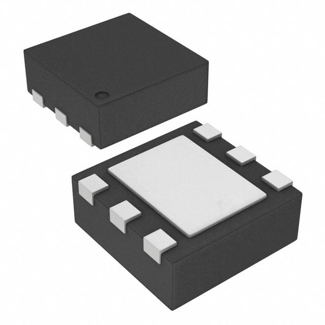
| 供应商器件封装 | 6-SON(2x2) |
| 其它名称 | 296-25729-6 |
| 制造商产品页 | http://www.ti.com/general/docs/suppproductinfo.tsp?distId=10&orderablePartNumber=TPS62261TDRVRQ1 |
| 包装 | Digi-Reel® |
| 同步整流器 | 是 |
| 安装类型 | 表面贴装 |
| 封装/外壳 | 6-WDFN 裸露焊盘 |
| 工作温度 | -40°C ~ 105°C |
| 标准包装 | 1 |
| 电压-输入 | 2 V ~ 6 V |
| 电压-输出 | 1.8V |
| 电流-输出 | 600mA |
| 类型 | 降压(降压) |
| 输出数 | 1 |
| 输出类型 | 固定 |
| 频率-开关 | 2.25MHz |


- 商务部:美国ITC正式对集成电路等产品启动337调查
- 曝三星4nm工艺存在良率问题 高通将骁龙8 Gen1或转产台积电
- 太阳诱电将投资9.5亿元在常州建新厂生产MLCC 预计2023年完工
- 英特尔发布欧洲新工厂建设计划 深化IDM 2.0 战略
- 台积电先进制程称霸业界 有大客户加持明年业绩稳了
- 达到5530亿美元!SIA预计今年全球半导体销售额将创下新高
- 英特尔拟将自动驾驶子公司Mobileye上市 估值或超500亿美元
- 三星加码芯片和SET,合并消费电子和移动部门,撤换高东真等 CEO
- 三星电子宣布重大人事变动 还合并消费电子和移动部门
- 海关总署:前11个月进口集成电路产品价值2.52万亿元 增长14.8%


PDF Datasheet 数据手册内容提取
TPS62260-Q1, TPS62261-Q1 TPS62262-Q1, TPS62263-Q1 www.ti.com SLVSA16C–AUGUST2009–REVISEDJULY2012 2.25-MHz 600-mA STEP-DOWN CONVERTERS CheckforSamples:TPS62260-Q1,TPS62261-Q1,TPS62262-Q1,TPS62263-Q1 FEATURES 1 • QualifiedforAutomotiveApplications • SoftStart 2 • High-EfficiencyStep-DownConverter • VoltagePositioningatLightLoads • OutputCurrentupto600mA • AvailableinaSmall2×2×0,8-mmSONPackage • WideV Rangefrom2-Vto6-VforLi-Ion • Allows<1-mmSolutionHeight IN BatterieswithExtendedVoltageRange APPLICATIONS • 2.25-MHzFixedFrequencyOperation • PowerSaveModeatLightLoadCurrents • PDAs,PocketPCs • OutputVoltageAccuracyinPWMMode±1.5% • LowPowerDSPSupply • 15-μA(Typ)QuiescentCurrent • PortableMediaPlayers • 100%DutyCycleforLowestDropout • POLapplications DESCRIPTION The TPS6226x devices are high-efficiency synchronous step-down dc-dc converters optimized for battery powered applications. It provides up to 600-mA output current from a single Li-Ion cell and is ideal to power mobilephonesandotherportableapplications. With an wide input voltage range of 2 V to 6 V, the device supports applications powered by Li-Ion batteries with extendedvoltagerange,twoandthreecellalkalinebatteries,3.3-Vand5-Vinputvoltagerails. The TPS6226x operates at 2.25-MHz fixed switching frequency and enters Power Save Mode operation at light loadcurrentstomaintainhighefficiencyovertheentireloadcurrentrange. The Power Save Mode is optimized for low output voltage ripple. For low noise applications, the device can be forced into fixed frequency PWM mode by pulling the MODE pin high. In the shutdown mode, the current consumption is reduced to less than 1 μA. TPS6226x allows the use of small inductors and capacitors to achieve asmallsolutionsize. TheTPS6226xisavailableinaverysmall2×2mm6-pinSONpackage. VIN= 2V to 6V TPS62260DRV 2.2LmH Up to 600mA 100 VIN= 2.3 V VIN SW VOUT 90 V = 2.7 V 4.7CmINF EN R1 C221 pF C10OmUFT 80VININ= 3 V GND FB 70 VIN= 3.6 V MODE R2 y - % 60 VIN= 4.5 V nc 50 e ci Effi 40 30 V = 1.8 V, OUT MODE = GND, 20 L= 2.2mH, DCR 110 mR 10 0 0.01 0.1 1 10 100 1000 I - Output Current - mA O 1 Pleasebeawarethatanimportantnoticeconcerningavailability,standardwarranty,anduseincriticalapplicationsof TexasInstrumentssemiconductorproductsanddisclaimerstheretoappearsattheendofthisdatasheet. PowerPADisatrademarkofTexasInstruments. 2 PRODUCTIONDATAinformationiscurrentasofpublicationdate. Copyright©2009–2012,TexasInstrumentsIncorporated Products conform to specifications per the terms of the Texas Instruments standard warranty. Production processing does not necessarilyincludetestingofallparameters.
TPS62260-Q1, TPS62261-Q1 TPS62262-Q1, TPS62263-Q1 SLVSA16C–AUGUST2009–REVISEDJULY2012 www.ti.com This integrated circuit can be damaged by ESD. Texas Instruments recommends that all integrated circuits be handled with appropriateprecautions.Failuretoobserveproperhandlingandinstallationprocedurescancausedamage. ESDdamagecanrangefromsubtleperformancedegradationtocompletedevicefailure.Precisionintegratedcircuitsmaybemore susceptibletodamagebecauseverysmallparametricchangescouldcausethedevicenottomeetitspublishedspecifications. ORDERINGINFORMATION(1) T OUTPUT PACKAGE(2) ORDERABLEPARTNUMBER TOP-SIDEMARKING A VOLTAGE –40°Cto85°C Adjustable TPS62260IDRVRQ1 OEO 1.8V TPS62261TDRVRQ1 OFE –40°Cto105°C 1.2V SON–DRV Reelof3000 TPS62262TDRVRQ1 OFF 2.5V TPS62263TDRVRQ1 OFG –40°Cto105°C Adjustable TPS62260TDRVRQ1 OEO (1) Forthemostcurrentpackageandorderinginformation,seethePackageOptionAddendumattheendofthisdocument,orseetheTI websiteatwww.ti.com. (2) Packagedrawings,thermaldata,andsymbolizationareavailableatwww.ti.com/packaging. ABSOLUTE MAXIMUM RATINGS(1) overoperatingfree-airtemperaturerange(unlessotherwisenoted) Inputvoltagerange(2) –0.3Vto7V VoltagerangeatEN,MODE –0.3VtoV +0.3V,≤7V IN VoltageonSW –0.3Vto7V Peakoutputcurrent Internallylimited HBM,Human-bodymodel 2000V ESDrating(3) CDM,Charged-devicemodel 1000V MM,Machinemodel 200V T Operatingjunctiontemperature –40°Cto125°C J T Storagetemperaturerange –65°Cto150°C stg (1) Stressesbeyondthoselistedunderabsolutemaximumratingsmaycausepermanentdamagetothedevice.Thesearestressratings onlyandfunctionaloperationofthedeviceattheseoranyotherconditionsbeyondthoseindicatedunderrecommendedoperating conditionsisnotimplied.Exposuretoabsolute-maximum-ratedconditionsforextendedperiodsmayaffectdevicereliability. (2) Allvoltagevaluesarewithrespecttonetworkgroundterminal. (3) Thehumanbodymodelisa100-pFcapacitordischargedthrougha1.5-kΩresistorintoeachpin.Themachinemodelisa200-pF capacitordischargeddirectlyintoeachpin. DISSIPATION RATINGS PACKAGE R POWERRATINGFORT ≤25°C DERATINGFACTORABOVET =25°C θJA A A DRV 76°C/W 1300mW 13mW/°C RECOMMENDED OPERATING CONDITIONS MIN NOM MAX UNIT V Supplyvoltage 2 6 V IN Outputvoltagerangeforadjustablevoltage 0.6 VIN V T Operatingambienttemperature TPS62260IDRVRQ1 –40 85 °C A TPS6226XTDRVRQ1 -40 105 T Operatingjunctiontemperature –40 125 °C J 2 SubmitDocumentationFeedback Copyright©2009–2012,TexasInstrumentsIncorporated ProductFolderLink(s):TPS62260-Q1 TPS62261-Q1TPS62262-Q1 TPS62263-Q1
TPS62260-Q1, TPS62261-Q1 TPS62262-Q1, TPS62263-Q1 www.ti.com SLVSA16C–AUGUST2009–REVISEDJULY2012 ELECTRICAL CHARACTERISTICS Overfulloperatingambienttemperaturerange,typicalvaluesareatT =25°C.Unlessotherwisenoted,specificationsapply A forconditionV =EN=3.6V.ExternalcomponentsC =4.7μF0603,C =10μF0603,L=2.2μH,seetheparameter IN IN OUT measurementinformation. PARAMETER TESTCONDITIONS MIN TYP MAX UNIT Supply V Inputvoltagerange 2.3 6 V IN V 2.5Vto6V 600 IN I Outputcurrent(1) V 2.3Vto2.5V 300 mA OUT IN V 2Vto2.3V 150 IN I =0mA,PFMmodeenabled(MODE=GND), OUT 15 devicenotswitching μA I =0mA,PFMmode(2)enabled(MODE=GND), I Operatingquiescentcurrent OUT 18.5 Q deviceswitching,V =1.8V OUT I =0mA,switchingwithnoload(MODE=V ), OUT IN 3.8 mA PWMoperation,V =1.8V,V =3V OUT IN T =25°C 0.1 1 A I Shutdowncurrent EN=GND μA SD T =105°C 2.5 A Falling 1.85 UVLO Undervoltagelockoutthreshold V Rising 1.95 Enable,Mode V Highlevelinputvoltage,EN,MODE 2V≤V ≤6V 1 VIN V IH IN V Lowlevelinputvoltage,EN,MODE 2V≤V ≤6V 0 0.4 V IL IN I Inputbiascurrent,EN,MODE EN,MODE=GNDorVIN 0.01 1 μA IN PowerSwitch High-sideMOSFETon-resistance 240 480 R V =V =3.6V,T =25°C mΩ DS(on) IN GS A Low-sideMOSFETon-resistance 185 380 ForwardcurrentlimitMOSFET,high I V =V =3.6V,T =25°C 0.8 1 1.3 A LIMF sideandlowside IN GS A Thermalshutdown Increasingjunctiontemperature 140 T °C SD Thermalshutdownhysteresis Decreasingjunctiontemperature 20 Oscillator f Oscillatorfrequency 2V≤V ≤6V 2 2.25 2.5 MHz SW IN Output V Adjustableoutputvoltagerange 0.6 V V OUT IN V Referencevoltage 600 mV ref MODE=V ,PWMoperation, IN FeedbackvoltagePWMmode forfixedoutputvoltageversionsV =V , –1.5% 0% 1.5% FB OUT 2.5V≤V ≤6V,0mA≤I ≤600mA (3) IN OUT V FB MODE=GND,deviceinPFMmode, FeedbackvoltagePFMmode voltagepositioningactive(2) 1% Loadregulation PWMMode -0.5 %/A t Start-uptime TimefromactiveENtoreach95%ofV nominal 500 μs StartUp OUT t V ramp-uptime Timetorampfrom5%to95%ofV 250 μs Ramp OUT OUT I LeakagecurrentintoSWpin V =3.6V,V =V =V ,EN=GND (4) 0.1 1 μA lkg IN IN OUT SW (1) Notproductiontested (2) InPFMmode,theinternalreferencevoltageissettotyp.1.01×V .Seetheparametermeasurementinformation. ref (3) ForV =V +0.6V IN O (4) Infixedoutputvoltageversions,theinternalresistordividernetworkisdisconnectedfromFBpin. Copyright©2009–2012,TexasInstrumentsIncorporated SubmitDocumentationFeedback 3 ProductFolderLink(s):TPS62260-Q1 TPS62261-Q1TPS62262-Q1 TPS62263-Q1
TPS62260-Q1, TPS62261-Q1 TPS62262-Q1, TPS62263-Q1 SLVSA16C–AUGUST2009–REVISEDJULY2012 www.ti.com PIN ASSIGNMENTS DRVPACKAGE (TOP VIEW) SW 1 Exposed 6 GND MODE 2 Thermal 5 VIN Pad FB 3 4 EN TERMINALFUNCTIONS TERMINAL I/O DESCRIPTION NAME NO. ThisistheswitchpinandisconnectedtotheinternalMOSFETswitches.Connecttheexternalinductor SW 1 OUT betweenthisterminalandtheoutputcapacitor. ThispinisonlyavailableatSONpackageoption.MODEpin=highforcesthedevicetooperateinfixed MODE 2 I frequencyPWMmode.MODEpin=lowenablesthePowerSaveModewithautomatictransitionfrom PFMmodetofixedfrequencyPWMmode. Feedbackfortheinternalregulationloop.Connecttheexternalresistordividertothispin.Incaseof FB 3 I fixedoutputvoltageoption,connectthispindirectlytotheoutputcapacitor. Thisistheenablepinofthedevice.Pullingthispintolowforcesthedeviceintoshutdownmode.Pulling EN 4 I thispintohighenablesthedevice.Thispinmustbeterminated. V 5 PWR Powersupply IN GND 6 PWR Ground FUNCTIONAL BLOCK DIAGRAM V IN Current- Limit Comparator V Thermal Undervoltage IN Shutdown Lockout1.8V Limit EN High Side PFM Comparator Reference +1%Voltage positioning 0.6V VREF FB VREF+1% Only in 2x2SON Gate Driver MODE MODE Control ShootA-Tnhtir-ough ErrorAmplifier Stage Softstart SW1 VOUTRAMP VREF CONTROL Integrator FB FB PWM Zero-Pole Comp. Amp. Limit RI1 GND Low Side RI..N RI3 Sawtooth 2.25-MHz CLiumrrite Cnto-mparator Generator Oscillator Int.Resistor Network GND 4 SubmitDocumentationFeedback Copyright©2009–2012,TexasInstrumentsIncorporated ProductFolderLink(s):TPS62260-Q1 TPS62261-Q1TPS62262-Q1 TPS62263-Q1
TPS62260-Q1, TPS62261-Q1 TPS62262-Q1, TPS62263-Q1 www.ti.com SLVSA16C–AUGUST2009–REVISEDJULY2012 PARAMETER MEASUREMENT INFORMATION TPS62260DVR L 2.2mH VOUT VIN SW CIN EN R1 C1 C 4.7mF 22 pF OUT 10mF FB GND R MODE 2 L: LPS3015 2.2mH, 110 mW C GRM188R60J475K 4.7mF Murata 0603 size IN C GRM188R60J106M 10mF Murata 0603 size OUT Copyright©2009–2012,TexasInstrumentsIncorporated SubmitDocumentationFeedback 5 ProductFolderLink(s):TPS62260-Q1 TPS62261-Q1TPS62262-Q1 TPS62263-Q1
TPS62260-Q1, TPS62261-Q1 TPS62262-Q1, TPS62263-Q1 SLVSA16C–AUGUST2009–REVISEDJULY2012 www.ti.com TYPICAL CHARACTERISTICS Table1.TableofGraphs FIGURE OutputCurrentV =1.8V,PowerSaveMode,MODE=GND Figure1 OutputCurrentVOUT=1.8V,PWMMode,MODE=V Figure2 η Efficiency OOuuttppuuttCCuurrrreennttVVOOUUTT==33..33VV,,PPWowMerMSoadvee,MMoOdDeE,M=OVDIINNE=GND FFiigguurree34 OutputCurrent OUT Figure5 OutputCurrent Figure6 at25°C,V =1.8V,PowerSaveMode,MODE=GND Figure7 at–40°C,VOUT =1.8V,PowerSaveMode,MODE=GND Figure8 OutputVoltageAccuracy aatt8255°°CC,,VVOOUTUT==11..88VV,,PPoWwMerMSoadvee,MMoOdDeE,M=OVDE=GND FFigiguurree190 at–40°C,VOUT =1.8V,PWMMode,MODE=VIN Figure11 at85°C,V OUT=1.8V,PWMMode,MODE=V IN Figure12 TypicalOperation PWMModOeU,TV =1.8V IN Figure13 ModeTransition MMOODDEEPPiinnTTrraaOnnUssiiTttiioonnFFrroommPFoFrMcetdoPFWorMcedtoPPWFMMMMooddeeaattlliigghhttllooaadd FFiigguurree1145 Start-upTiming Figure16 ForcedPWMMode,V =1.5V,50mAto200mA Figure17 ForcedPWMMode,VOUT=1.5V,200mAto400mA Figure18 PFMModetoPWMMoOdUeT,V =1.5V,150μAto400mA Figure19 PWMModetoPFMMode,VOUT=1.5V,400mAto150μA Figure20 LoadTransient PFMMode,V =1.5V,1.5OUmTAto50mA Figure21 PFMMode,VOUT=1.5V,50mAto1.5mA Figure22 PFMModetoOPUWTMMode,V =1.8V,50mAto250mA Figure23 PFMModetoPWMMode,VOUT=1.5V,50mAto400mA Figure24 PWMModetoPFMMode,VOUT=1.5V,400mAto50mA Figure25 LineTransient PPFFMMMMooddee,,VVOUT==11..88VV,,5205O0mUmTAA FFiigguurree2267 TypicalOperation PPFFMMVVOUTRRiippOppUlleeT,,VVOUT==11..88VV,,1100mmAA,,LL==24..27μμHH,,CCOUT==1100μμFF FFiigguurree2289 ShutdownCurrentintoVIN vsInpuOtUVToltage,(TO=UT85°C,T =25°C,T =-40°C) OUT Figure30 QuiescentCurrent vsInputVoltage,(TA=85°C,TA=25°C,TA=-40°C) Figure31 SRteastiisctaDnraceinSourceOn-State vsInputVoltage,(TAA=85°C,TAA=25°C,TAA=-40°C) FFiigguurree3323 EFFICIENCY(PowerSaveMode) EFFICIENCY(PWMMode) vs vs OUTPUTCURRENT OUTPUTCURRENT 100 100 90 90 V = 2.3 V IN 80 80 V = 2.7 V IN 70 70 % ncy - % 5600 ciency - 5600 VIN= 3 V VVININ== 43..56 VV cie Effi Effi 40 - h 40 30 30 V = 1.8 V OUT 20 MODE = GND 20 VOUT= 1.8 V, L= 2.2mH MODE = V , IN 10 DCR 110 mR 10 L= 2.2mH 0 0 0.01 0.1 1 10 100 1000 1 10 100 1000 IO- Output Current - mA IO- Output Current - mA Figure1. Figure2. 6 SubmitDocumentationFeedback Copyright©2009–2012,TexasInstrumentsIncorporated ProductFolderLink(s):TPS62260-Q1 TPS62261-Q1TPS62262-Q1 TPS62263-Q1
TPS62260-Q1, TPS62261-Q1 TPS62262-Q1, TPS62263-Q1 www.ti.com SLVSA16C–AUGUST2009–REVISEDJULY2012 EFFICIENCY(PWMMode) EFFICIENCY(PowerSaveMode) vs vs OUTPUTCURRENT OUTPUTCURRENT 100 100 V = 4.2 V IN 90 VIN= 4.2 V 90 V = 3.6 V IN 80 VIN= 3.6 V 80 VIN= 5 V 70 V = 5 V 70 V = 4.5 V % IN % IN – 60 V = 4.5 V – 60 y IN y c c n n e 50 e 50 ci ci Effi 40 Effi 40 – – h 30 VOUT= 3.3 V h 30 VOUT= 3.3 V MODE = VIN MODE = GND 20 L= 2.2mH 20 L= 2.2mH DCR 110 mW DCR = 110 mH 10 C = 10mF 0603 10 C = 10mF 0603 OUT OUT 0 0 1 10 100 1000 0.01 0.1 1 10 100 1000 I –Output Current–mA OUT I –Output Current–mA OUT Figure3. Figure4. EFFICIENCY EFFICIENCY vs vs OUTPUTCURRENT OUTPUTCURRENT 100 100 90 90 V = 2.3 V I V = 2.7 V I 80 80 V = 4.5 V I 70 V = 2.3 V 70 I % VI = 2.3 V % VI = 3.6 V − 60 V = 4.5 V − 60 y I y cienc 50 VI = 3.6 V cienc 50 VI = 2.7 V Effi 40 Effi 40 30 VO= 1.2 V, 30 VO= 1.2 V MODE = VI, MODE = GND 20 L= 2mH, 20 L= 2mH MIPSA2520 MIPSA2520 10 CO= 10mF 0603 10 CO= 10mF 0603 0 0 1 10 100 1000 0.01 0.1 1 10 100 1000 IO−Output Current−mA IO−Output Current−mA Figure5. Figure6. Copyright©2009–2012,TexasInstrumentsIncorporated SubmitDocumentationFeedback 7 ProductFolderLink(s):TPS62260-Q1 TPS62261-Q1TPS62262-Q1 TPS62263-Q1
TPS62260-Q1, TPS62261-Q1 TPS62262-Q1, TPS62263-Q1 SLVSA16C–AUGUST2009–REVISEDJULY2012 www.ti.com OUTPUTVOLTAGEACCURACY OUTPUTVOLTAGEACCURACY(PowerSaveMode) vs vs OUTPUTCURRENT OUTPUTCURRENT 1.88 1.88 1.86 1.86 V PFM Mode, Voltage Positioning V – 1.84 – 1.84 C C D D e e g g a 1.82 a 1.82 olt olt V V ut ut p 1.8 p 1.8 ut ut O O –O 1.78 TA= 25°C –O 1.78 TA=–40°C V V = 1.8 V V V = 1.8 V OUT OUT MODE = GND MODE = GND 1.76 1.76 L= 2.2mH L= 2.2mH C = 10mF C = 10mF O O 1.74 1.74 0.01 0.1 1 10 100 1000 0.01 0.1 1 10 100 1000 I –Output Current–mA I –Output Current–mA O O Figure7. Figure8. OUTPUTVOLTAGEACCURACY(PowerSaveMode) OUTPUTVOLTAGEACCURACY(PWMMode) vs vs OUTPUTCURRENT OUTPUTCURRENT 1.88 1.854 T = 25°C, A V = 1.8 V, 1.86 1.836 OUT MODE = V , IN DC–V 1.84 DC - V 1.818 L= 2.2mH Voltage 1.82 Voltage 1.8 –Output O 1.17.88 TA= 85°C V- Output O1.782 VVIIVNNIN== =22.. 373 VVV V VOUT= 1.8 V VIN= 3.6 V MODE = GND 1.764 VIN= 4.5 V 1.76 L= 2.2mH C = 10mF O 1.74 1.746 0.01 0.1 1 10 100 1000 0.01 0.1 1 10 100 1000 IO–Output Current–mA IO- Output Current - mA Figure9. Figure10. 8 SubmitDocumentationFeedback Copyright©2009–2012,TexasInstrumentsIncorporated ProductFolderLink(s):TPS62260-Q1 TPS62261-Q1TPS62262-Q1 TPS62263-Q1
TPS62260-Q1, TPS62261-Q1 TPS62262-Q1, TPS62263-Q1 www.ti.com SLVSA16C–AUGUST2009–REVISEDJULY2012 OUTPUTVOLTAGEACCURACY(PWMMode) OUTPUTVOLTAGEACCURACY(PWMMode) vs vs OUTPUTCURRENT OUTPUTCURRENT 1.854 1.854 TA= -40°C, TA= 85°C, VOUT= 1.8 V, VOUT= 1.8 V, 1.836 MODE = VIN, 1.836 MODE = VIN, V L= 2.2mH V L= 2.2mH C - C - D 1.818 D 1.818 e e g g a a olt olt V 1.8 V 1.8 ut V = 2 V ut p IN p Out VIN= 2.7 V Out VIN= 2.3 V - O1.782 VIN= 3 V - O1.782 VIN= 2.7 V V VIN= 3.6 V V VIN= 3 V 1.764 VIN= 4.5 V 1.764 VIN= 3.6 V V = 4.5 V IN 1.746 1.746 0.01 0.1 1 10 100 1000 0.01 0.1 1 10 100 1000 I - Output Current - mA I - Output Current - mA O O Figure11. Figure12. MODEPINTRANSITIONFROMPFM TYPICALOPERATION(PWMMode) TOFORCEDPWMMODEATLIGHTLOAD V 3.6V IN V = 3.6 V V 1.8V, I 150mA IN VOUT10 mV/Div LO2U.2TmH, COUOTUT10mF 0603 M2VO/DDiEv VIOOUUTT== 1 10. 8m VA SW 2 V/Div SW 2V/Div PFM Mode Forced PWM Mode I 200 mA/Div COIL I coil 200mA/Div Time Base - 10ms/Div Time Base - 1ms/Div Figure13. Figure14. Copyright©2009–2012,TexasInstrumentsIncorporated SubmitDocumentationFeedback 9 ProductFolderLink(s):TPS62260-Q1 TPS62261-Q1TPS62262-Q1 TPS62263-Q1
TPS62260-Q1, TPS62261-Q1 TPS62262-Q1, TPS62263-Q1 SLVSA16C–AUGUST2009–REVISEDJULY2012 www.ti.com MODEPINTRANSITIONFROMPWM TOPFMMODEATLIGHTLOAD START-UPTIMING M2 OV/DDEiv VIN= 3.6 V EN 2 V/Div VIN= 3.6 V VOUT= 1.8 V RLoad= 10Ω IOUT= 10 mA VOUT= 1.8 V I into C IN IN SW MODE = GND 2 V/Div SW 2 V/Div Forced PWM Mode PFM Mode V 2 V/Div OUT I COIL 200 mA/Div I 100 mA/Div IN Time Base - 2.5ms/Div Time Base - 100ms/Div Figure15. Figure16. LOADTRANSIENT LOADTRANSIENT (ForcedPWMMode) (ForcedPWMMode) V 3.6 V V 3.6 V IN IN V 1.5 V V 50 mV/Div V 1.5 V OUT OUT OUT V 50 mV/Div I 50 mAto 200 mA I 200 mAto 400 mA OUT OUT OUT MODE =V IN IOUT 200 mA/Div 400 mA I 200 mA/Div 200 mA OUT I 500 mA/Div COIL I 500 mA/Div COIL Time Base - 20ms/Div Time Base - 20ms/Div Figure17. Figure18. 10 SubmitDocumentationFeedback Copyright©2009–2012,TexasInstrumentsIncorporated ProductFolderLink(s):TPS62260-Q1 TPS62261-Q1TPS62262-Q1 TPS62263-Q1
TPS62260-Q1, TPS62261-Q1 TPS62262-Q1, TPS62263-Q1 www.ti.com SLVSA16C–AUGUST2009–REVISEDJULY2012 LOADTRANSIENT LOADTRANSIENT (ForcedPFMModeToPWMMode) (ForcedPWMModeToPFMMode) SW 2 V/Div SW 2 V/Div V 3.6 V IN V 1.5 V V 3.6 V OUT VOUT50mV/Div VIONUT1.5 V IMOOUTDE15 =0 GmANDto 400 mA IOUT150mAto 400 mA VOUT50 mV/Div MODE = GND I 500 mA/Div 400 mA 400 mA OUT I 500 mA/Div OUT 150mA 150mA ICOILl500mA/Div ICOIL500 mA/Div Time Base–500ms/Div Time Base–500ms/Div Figure19. Figure20. LOADTRANSIENT(PFMMode) LOADTRANSIENT(PFMMode) SW 2 V/Div SW 2 V/Div VIN3.6 V VIN3.6 V VOUT1.5 V VOUT1.5 V IMOOUTDE1 .=5 GmNADto 50 mA VOUT50 mV/Div IMOOUTD5E0 = m GANtoD1.5mA V 50mV/Div OUT 50 mA 50 mA I 50 mA/Div I 50 mA/Div OUT OUT 1.5 mA 1.5 mA ICOIL500 mA/Div ICOIL500 mA/Div Time Base–50ms/Div Time Base–50ms/Div Figure21. Figure22. Copyright©2009–2012,TexasInstrumentsIncorporated SubmitDocumentationFeedback 11 ProductFolderLink(s):TPS62260-Q1 TPS62261-Q1TPS62262-Q1 TPS62263-Q1
TPS62260-Q1, TPS62261-Q1 TPS62262-Q1, TPS62263-Q1 SLVSA16C–AUGUST2009–REVISEDJULY2012 www.ti.com LOADTRANSIENT LOADTRANSIENT (PFMModeToPWMMode) (PFMModeToPWMMode) SW 2 V/Div SW 2 V/Div VOUT50 mV/Div VIN3.6 V VIN3.6 V VOUT50 mV/Div VIOUT510.5m VAto 400 mA V 1.8 V OUT OUT MODE = GND I 50mAto 250 mA OUT MODE = GND 250 mA PFM Mode PWM Mode 400 mA IOUT200 mA/Div IOUT500 mA/Div 50 mA 50 mA ICOIL 500 mA/Div ICOIL 500mA/Div Time Base–20ms/Div Time Base–20ms/Div Figure23. Figure24. LOADTRANSIENT (PWMModeToPFMMode) LINETRANSIENT(PFMMode) SW 2 V/Div V 3.6V to 4.2V IN 500 mV/Div V 3.6 V IN V 1.5 V V 50 mV/Div OUT OUT I 50mAto 400 mA OUT MODE = GND PFM Mode PWM Mode I 500 mA/Div 400 mA OUT V = 1.8 V OUT 50 mA 50 mV/Div I = 50 mA OUT MODE = GND I 500 mA/Div COIL Time Base–20ms/Div Figure25. Figure26. 12 SubmitDocumentationFeedback Copyright©2009–2012,TexasInstrumentsIncorporated ProductFolderLink(s):TPS62260-Q1 TPS62261-Q1TPS62262-Q1 TPS62263-Q1
TPS62260-Q1, TPS62261-Q1 TPS62262-Q1, TPS62263-Q1 www.ti.com SLVSA16C–AUGUST2009–REVISEDJULY2012 LINETRANSIENT(PWMMode) TYPICALOPERATION(PFMMode) VIN3.6V to 4.2V VOUT20 mV/Div 500 mV/Div SW 2 V/Div V = 1.8 V OUT 50 mV/Div I = 250 mA OUT MODE = VIN I 200 mA/Div COIL Time Base–100ms/Div Time Base–10ms/Div Figure27. Figure28. SHUTDOWNCURRENTINTOVIN vs TYPICALOPERATION(PFMMode) INPUTVOLTAGE V 3.6 V; V 1.8 V, I 10mA, 0.8 IN OUT OUT L= 4.7mH, C = 10mF 0603, EN = GND VOUT20 mV/Div MODE = GNDOUT 0.7 A m − N 0.6 VI T = 85oC SW 2 V/Div nto 0.5 A nt I e rr 0.4 u C n w 0.3 o I 200 mA/Div d COIL ut h 0.2 S - T = 25oC T = -40oC D A A IS 0.1 Time Base–2ms/Div 0 2 2.5 3 3.5 4 4.5 5 5.5 6 V −Input Voltage−V IN Figure29. Figure30. Copyright©2009–2012,TexasInstrumentsIncorporated SubmitDocumentationFeedback 13 ProductFolderLink(s):TPS62260-Q1 TPS62261-Q1TPS62262-Q1 TPS62263-Q1
TPS62260-Q1, TPS62261-Q1 TPS62262-Q1, TPS62263-Q1 SLVSA16C–AUGUST2009–REVISEDJULY2012 www.ti.com QUIESCENTCURRENT STATICDRAIN-SOURCEON-STATERESISTANCE vs vs INPUTVOLTAGE INPUTVOLTAGE 2200 W 0.8 MMOODDEE == GGNNDD, − High Side Switching EENN == VVIINN, e c 0.7 1188 DDeevviiccee NNoott SSwwiittcchhiinngg TTAA== 8855°oCC an st A A si 0.6 I–Quiescent Current–mQ I- Quiescent Current−m111111Q462246 TTTTAAAA==== – -22445500o°Co°CCC c Drain-Source On-State Re 0000....2345 T = -40oC TA = 85oCTA = 25oC 1100 Stati 0.1 A - n) 88222 22..55 33 33..55 44 44..55 55 55..55 66 DS(o 02 2.5 3 3.5 4 4.5 5 R VV –−InInppuutt V Vooltltaaggee–−VV V −Input Voltage−V IINN IN Figure31. Figure32. STATICDRAIN-SOURCEON-STATERESISTANCE vs INPUTVOLTAGE 0.4 W − Low Side Switching e c 0.35 n a st si 0.3 e R T = 85oC e A at 0.25 St n- TA = 25oC O 0.2 e c r u o 0.15 S n- ai r 0.1 D c T = -40oC Stati 0.05 A - n) o 0 DS( 2 2.5 3 3.5 4 4.5 5 R V −Input Voltage−V IN Figure33. 14 SubmitDocumentationFeedback Copyright©2009–2012,TexasInstrumentsIncorporated ProductFolderLink(s):TPS62260-Q1 TPS62261-Q1TPS62262-Q1 TPS62263-Q1
TPS62260-Q1, TPS62261-Q1 TPS62262-Q1, TPS62263-Q1 www.ti.com SLVSA16C–AUGUST2009–REVISEDJULY2012 DETAILED DESCRIPTION OPERATION The TPS6226x step down converter operates with typically 2.25 MHz fixed frequency pulse width modulation (PWM) at moderate to heavy load currents. At light load currents the converter can automatically enter Power SaveModeandoperatestheninPFMmode. During PWM operation the converter use a unique fast response voltage mode control scheme with input voltage feed-forward to achieve good line and load regulation allowing the use of small ceramic input and output capacitors. At the beginning of each clock cycle initiated by the clock signal, the High Side MOSFET switch is turned on. The current flows now from the input capacitor via the High Side MOSFET switch through the inductor to the output capacitor and load. During this phase, the current ramps up until the PWM comparator trips and the control logic will turn off the switch. The current limit comparator will also turn off the switch in case the current limit of the High Side MOSFET switch is exceeded. After a dead time preventing shoot through current, the Low Side MOSFET rectifier is turned on and the inductor current will ramp down. The current flows now from the inductor to the output capacitor and to the load. It returns back to the inductor through the Low Side MOSFET rectifier. ThenextcyclewillbeinitiatedbytheclocksignalagainturningofftheLowSideMOSFETrectifierandturningon theontheHighSideMOSFETswitch. POWER SAVE MODE The Power Save Mode is enabled with MODE Pin set to low level. If the load current decreases, the converter will enter Power Save Mode operation automatically. During Power Save Mode the converter skips switching and operateswithreducedfrequencyinPFMmodewithaminimumquiescentcurrenttomaintainhighefficiency.The converterwillpositiontheoutputvoltagetypically+1%abovethenominaloutputvoltage.Thisvoltagepositioning featureminimizesvoltagedropscausedbyasuddenloadstep. The transition from PWM mode to PFM mode occurs once the inductor current in the Low Side MOSFET switch becomeszero,whichindicatesdiscontinuousconductionmode. During the Power Save Mode the output voltage is monitored with a PFM comparator. As the output voltage falls below the PFM comparator threshold of V nominal +1%, the device starts a PFM current pulse. The High OUT Side MOSFET switch will turn on, and the inductor current ramps up. After the On-time expires, the switch is turnedoffandtheLowSideMOSFETswitchisturnedonuntiltheinductorcurrentbecomeszero. The converter effectively delivers a current to the output capacitor and the load. If the load is below the delivered current, the output voltage will rise. If the output voltage is equal or higher than the PFM comparator threshold, thedevicestopsswitchingandentersasleepmodewithtypical15μAcurrentconsumption. If the output voltage is still below the PFM comparator threshold, a sequence of further PFM current pulses are generated until the PFM comparator threshold is reached. The converter starts switching again once the output voltagedropsbelowthePFMcomparatorthreshold. With a fast single threshold comparator, the output voltage ripple during PFM mode operation can be kept small. The PFM Pulse is time controlled, which allows to modify the charge transferred to the output capacitor by the value of the inductor. The resulting PFM output voltage ripple and PFM frequency depend in first order on the size of the output capacitor and the inductor value. Increasing output capacitor values and inductor values will minimize the output ripple. The PFM frequency decreases with smaller inductor values and increases with larger values. The PFM mode is left and PWM mode entered in case the output current can not longer be supported in PFM mode.ThePowerSaveModecanbedisabledthroughtheMODEpinsettohigh.Theconverterwillthenoperate infixedfrequencyPWMmode. DynamicVoltagePositioning This feature reduces the voltage under/overshoots at load steps from light to heavy load and vice versa. It is active in Power Save Mode and regulates the output voltage 1% higher than the nominal value. This provides moreheadroomforboththevoltagedropataloadstep,andthevoltageincreaseataloadthrow-off. Copyright©2009–2012,TexasInstrumentsIncorporated SubmitDocumentationFeedback 15 ProductFolderLink(s):TPS62260-Q1 TPS62261-Q1TPS62262-Q1 TPS62263-Q1
TPS62260-Q1, TPS62261-Q1 TPS62262-Q1, TPS62263-Q1 SLVSA16C–AUGUST2009–REVISEDJULY2012 www.ti.com Output voltage Vout +1% Voltage Positioning PFM Comparator threshold Light load PFM Mode Vout (PWM) moderate to heavy load PWM Mode Figure34. PowerSaveModeOperationwithautomaticModetransition 100%DutyCycleLowDropoutOperation The device starts to enter 100% duty cycle mode once the input voltage comes close to the nominal output voltage. In order to maintain the output voltage, the High Side MOSFET switch is turned on 100% for one or morecycles. With further decreasing VIN the High Side MOSFET switch is turned on completely. In this case the converter offers a low input-to-output voltage difference. This is particularly useful in battery-powered applications to achievelongestoperationtimebytakingfulladvantageofthewholebatteryvoltagerange. The minimum input voltage to maintain regulation depends on the load current and output voltage, and can be calculatedas: V min=V max+I max× (R max+R ) IN O O DS(on) L With: I max=maximumoutputcurrentplusinductorripplecurrent O R max=maximumP-channelswitchRDSon. DS(on) R =DCresistanceoftheinductor L V max=nominaloutputvoltageplusmaximumoutputvoltagetolerance O UndervoltageLockout The undervoltage lockout circuit prevents the device from malfunctioning at low input voltages and from excessive discharge of the battery and disables the output stage of the converter. The undervoltage lockout thresholdistypically1.85VwithfallingV . IN MODE SELECTION TheMODEpinallowsmodeselectionbetweenforcedPWMmodeandPowerSaveMode. Connecting this pin to GND enables the Power Save Mode with automatic transition between PWM and PFM mode. Pulling the MODE pin high forces the converter to operate in fixed frequency PWM mode even at light loadcurrents.Thisallowssimplefilteringoftheswitchingfrequencyfornoisesensitiveapplications.Inthismode, theefficiencyislowercomparedtothepowersavemodeduringlightloads. The condition of the MODE pin can be changed during operation and allows efficient power management by adjustingtheoperationmodeoftheconvertertothespecificsystemrequirements. 16 SubmitDocumentationFeedback Copyright©2009–2012,TexasInstrumentsIncorporated ProductFolderLink(s):TPS62260-Q1 TPS62261-Q1TPS62262-Q1 TPS62263-Q1
TPS62260-Q1, TPS62261-Q1 TPS62262-Q1, TPS62263-Q1 www.ti.com SLVSA16C–AUGUST2009–REVISEDJULY2012 ENABLE The device is enabled setting EN pin to high. During the start up time t the internal circuits are settled and Start Up the soft start circuit is activated. The EN input can be used to control power sequencing in a system with various DC/DCconverters.TheENpincanbeconnectedtotheoutputofanotherconverter,todrivetheENpinhighand getting a sequencing of supply rails. With EN = GND, the device enters shutdown mode in which all internal circuits are disabled. In fixed output voltage versions, the internal resistor divider network is then disconnected fromFBpin. SOFT START The TPS6226x has an internal soft start circuit that controls the ramp up of the output voltage. The output voltage ramps up from 5% to 95% of its nominal value within typical 250μs. This limits the inrush current in the converter during ramp up and prevents possible input voltage drops when a battery or high impedance power sourceisused.Thesoftstartcircuitisenabledwithinthestartuptimet . StartUp SHORT-CIRCUIT PROTECTION The High Side and Low Side MOSFET switches are short-circuit protected with maximum switch current = I . LIMF The current in the switches is monitored by current limit comparators. Once the current in the High Side MOSFET switch exceeds the threshold of it's current limit comparator, it turns off and the Low Side MOSFET switch is activated to ramp down the current in the inductor and High Side MOSFET switch. The High Side MOSFET switch can only turn on again, once the current in the Low Side MOSFET switch has decreased below thethresholdofitscurrentlimitcomparator. THERMAL SHUTDOWN As soon as the junction temperature, T , exceeds 140°C (typical) the device goes into thermal shutdown. In this J mode, the High Side and Low Side MOSFETs are turned-off. The device continues its operation when the junctiontemperaturefallsbelowthethermalshutdownhysteresis. Copyright©2009–2012,TexasInstrumentsIncorporated SubmitDocumentationFeedback 17 ProductFolderLink(s):TPS62260-Q1 TPS62261-Q1TPS62262-Q1 TPS62263-Q1
TPS62260-Q1, TPS62261-Q1 TPS62262-Q1, TPS62263-Q1 SLVSA16C–AUGUST2009–REVISEDJULY2012 www.ti.com APPLICATION INFORMATION TPS62262DRV L1 V 1.2 V OUT V = 2 V to 6 V 2.2mH Up to 600 mA IN VIN SW C C IN EN OUT 4.7mF 10mF FB GND MODE Figure35. Fixed1.2-VOutput TPS62260DRV L 1 2.2mH V 1.2 V OUT VIN SW R C C 1 1 C IN EN 360 kW 22 pF OUT 4.7mF 10mF FB GND R 2 360 kW MODE Figure36. Adjustable1.2-VOutput TPS62260DRV L1 V 1.5 V OUT VIN= 2 V to 6 V 2.2mH Up to 600 mA VIN SW C R1 C1 IN EN 540 kΩ 22 pF 4.7mF C FB OUT GND 10mF R2 360 kΩ MODE Figure37. Adjustable1.5-VOutput 18 SubmitDocumentationFeedback Copyright©2009–2012,TexasInstrumentsIncorporated ProductFolderLink(s):TPS62260-Q1 TPS62261-Q1TPS62262-Q1 TPS62263-Q1
TPS62260-Q1, TPS62261-Q1 TPS62262-Q1, TPS62263-Q1 www.ti.com SLVSA16C–AUGUST2009–REVISEDJULY2012 TPS62261DRV L1 VOUT1.8 V V = 2 V to 6 V 2.2mH Up to 600 mA IN VIN SW C IN EN 4.7mF C OUT FB 10mF GND MODE Figure38. Fixed1.8-VOutput Copyright©2009–2012,TexasInstrumentsIncorporated SubmitDocumentationFeedback 19 ProductFolderLink(s):TPS62260-Q1 TPS62261-Q1TPS62262-Q1 TPS62263-Q1
TPS62260-Q1, TPS62261-Q1 TPS62262-Q1, TPS62263-Q1 SLVSA16C–AUGUST2009–REVISEDJULY2012 www.ti.com OUTPUT VOLTAGE SETTING Theoutputvoltagecanbecalculatedto: (cid:4) R (cid:5) 1 VOUT(cid:3)VREF(cid:1) 1(cid:2)R 2 withaninternalreferencevoltageV typical0.6V. REF To minimize the current through the feedback divider network, R should be 180 kΩ or 360 kΩ. The sum of R 2 1 and R should not exceed ~1MΩ, to keep the network robust against noise. An external feed forward capacitor 2 C is required for optimum load transient response. The value of C should be in the range between 22pF and 1 1 33pF. RoutetheFBlineawayfromnoisesources,suchastheinductorortheSWline. OUTPUT FILTER DESIGN (INDUCTOR AND OUTPUT CAPACITOR) TheTPS6226xisdesignedtooperatewithinductorsintherangeof1.5μHto4.7μHandwithoutputcapacitorsin therangeof4.7μFto22μF.Thepartisoptimizedforoperationwitha2.2μHinductorand10μFoutputcapacitor. Larger or smaller inductor values can be used to optimize the performance of the device for specific operation conditions. For stable operation, the L and C values of the output filter may not fall below 1μH effective inductanceand3.5μFeffectivecapacitance. InductorSelection The inductor value has a direct effect on the ripple current. The selected inductor has to be rated for its dc resistance and saturation current. The inductor ripple current (ΔI ) decreases with higher inductance and L increaseswithhigherV orV . I O TheinductorselectionhasalsoimpactontheoutputvoltagerippleinPFMmode.Higherinductorvalueswilllead to lower output voltage ripple and higher PFM frequency, lower inductor values will lead to a higher output voltageripplebutlowerPFMfrequency. Equation 1 calculates the maximum inductor current in PWM mode under static load conditions. The saturation current of the inductor should be rated higher than the maximum inductor current as calculated with Equation 2. This is recommended because during heavy load transient the inductor current will rise above the calculated value. V 1(cid:2) OUT V (cid:1)I (cid:3)V (cid:1) IN L OUT L(cid:1)f (1) (cid:1)I I max(cid:2)I max(cid:1) L L out 2 (2) With: f=SwitchingFrequency(2.25MHztypical) L=InductorValue ΔI =PeaktoPeakinductorripplecurrent L I =MaximumInductorcurrent Lmax A more conservative approach is to select the inductor current rating just for the switch current limit I of the LIMF converter. Accepting larger values of ripple current allows the use of lower inductance values, but results in higher output voltageripple,greatercorelosses,andloweroutputcurrentcapability. The total losses of the coil have a strong impact on the efficiency of the DC/DC conversion and consist of both thelossesinthedcresistance(R )andthefollowingfrequency-dependentcomponents: (DC) • Thelossesinthecorematerial(magnetichysteresisloss,especiallyathighswitchingfrequencies) • Additionallossesintheconductorfromtheskineffect(currentdisplacementathighfrequencies) • Magneticfieldlossesoftheneighboringwindings(proximityeffect) • Radiationlosses 20 SubmitDocumentationFeedback Copyright©2009–2012,TexasInstrumentsIncorporated ProductFolderLink(s):TPS62260-Q1 TPS62261-Q1TPS62262-Q1 TPS62263-Q1
TPS62260-Q1, TPS62261-Q1 TPS62262-Q1, TPS62263-Q1 www.ti.com SLVSA16C–AUGUST2009–REVISEDJULY2012 Table2.ListofInductors DIMENSIONS[mm3] InductanceμH INDUCTORTYPE SUPPLIER 2.5x2.0x1.0max 2.0 MIPS2520D2R2 FDK 2.5x2.0x1.2max 2.0 MIPSA2520D2R2 FDK 2.5x2.0x1.0max 2.2 KSLI-252010AG2R2 HtachiMetals 2.5x2.0x1.2max 2.2 LQM2HPN2R2MJ0L Murata 3x3x1.5max 2.2 LPS30152R2 Coilcraft OutputCapacitorSelection The advanced fast-response voltage mode control scheme of the TPS6226x allows the use of tiny ceramic capacitors. Ceramic capacitors with low ESR values have the lowest output voltage ripple and are recommended. The output capacitor requires either an X7R or X5R dielectric. Y5V and Z5U dielectric capacitors, asidefromtheirwidevariationincapacitanceovertemperature,becomeresistiveathighfrequencies. Atnominalloadcurrent,thedeviceoperatesinPWMmodeandtheRMSripplecurrentiscalculatedas: V OUT 1(cid:2) V IN 1 IRMSCOUT(cid:3)VOUT(cid:1) L(cid:1)f (cid:1)2(cid:1)(cid:4)3 (3) Atnominalloadcurrent,thedeviceoperatesinPWMmodeandtheoveralloutputvoltagerippleisthesumofthe voltagespikecausedbytheoutputcapacitorESRplusthevoltageripplecausedbycharginganddischargingthe outputcapacitor: V OUT 1(cid:3) V (cid:1)VOUT(cid:4)VOUT(cid:1) L(cid:1)IfN (cid:1)(cid:5)8(cid:1)C1out(cid:1)f(cid:2)ESR(cid:6) (4) At light load currents, the converter operates in Power Save Mode and the output voltage ripple is dependent on the output capacitor and inductor value. Larger output capacitor and inductor values minimize the voltage ripple inPFMmodeandtightenDCoutputaccuracyinPFMmode. InputCapacitorSelection An input capacitor is required for best input voltage filtering, and minimizing the interference with other circuits caused by high input voltage spikes. For most applications, a 4.7μF to 10μF ceramic capacitor is recommended. Because ceramic capacitor loses up to 80% of its initial capacitance at 5 V, it is recommended that 10μF input capacitors be used for input voltages > 4.5V. The input capacitor can be increased without any limit for better input voltage filtering. Take care when using only small ceramic input capacitors. When a ceramic capacitor is used at the input and the power is being supplied through long wires, such as from a wall adapter, a load step at the output or VIN step on the input can induce ringing at the VIN pin. This ringing can couple to the output and bemistakenasloopinstabilityorcouldevendamagethepartbyexceedingthemaximumratings. Table3.ListofCapacitors CAPACITANCE TYPE SIZE SUPPLIER 4.7μF GRM188R60J475K 06031.6x0.8x0.8mm3 Murata 10μF GRM188R60J106M69D 06031.6x0.8x0.8mm3 Murata Copyright©2009–2012,TexasInstrumentsIncorporated SubmitDocumentationFeedback 21 ProductFolderLink(s):TPS62260-Q1 TPS62261-Q1TPS62262-Q1 TPS62263-Q1
TPS62260-Q1, TPS62261-Q1 TPS62262-Q1, TPS62263-Q1 SLVSA16C–AUGUST2009–REVISEDJULY2012 www.ti.com LAYOUT CONSIDERATIONS Figure39. SuggestedLayoutforFixedOutputVoltageOptions GND V OUT 2 C1 R V R1 IN C OUT N L I C U D N G Figure40. SuggestedLayoutforAdjustableOutputVoltageVersion 22 SubmitDocumentationFeedback Copyright©2009–2012,TexasInstrumentsIncorporated ProductFolderLink(s):TPS62260-Q1 TPS62261-Q1TPS62262-Q1 TPS62263-Q1
TPS62260-Q1, TPS62261-Q1 TPS62262-Q1, TPS62263-Q1 www.ti.com SLVSA16C–AUGUST2009–REVISEDJULY2012 As for all switching power supplies, the layout is an important step in the design. Proper function of the device demands careful attention to PCB layout. Care must be taken in board layout to get the specified performance. If the layout is not carefully done, the regulator could show poor line and/or load regulation, stability issues as well as EMI problems. It is critical to provide a low inductance, impedance ground path. Therefore, use wide and short traces for the main current paths. The input capacitor should be placed as close as possible to the IC pins aswellastheinductorandoutputcapacitor. Connect the GND Pin of the device to the PowerPAD™ land of the PCB and use this pad as a star point. Use a common Power GND node and a different node for the Signal GND to minimize the effects of ground noise. Connect these ground nodes together to the PowerPAD land (star point) underneath the IC. Keep the common path to the GND PIN, which returns the small signal components and the high current of the output capacitors as shortaspossibletoavoidgroundnoise.TheFBlineshouldbeconnectedrighttotheoutputcapacitorandrouted awayfromnoisycomponentsandtraces(e.g.,SWline). Copyright©2009–2012,TexasInstrumentsIncorporated SubmitDocumentationFeedback 23 ProductFolderLink(s):TPS62260-Q1 TPS62261-Q1TPS62262-Q1 TPS62263-Q1
TPS62260-Q1, TPS62261-Q1 TPS62262-Q1, TPS62263-Q1 SLVSA16C–AUGUST2009–REVISEDJULY2012 www.ti.com REVISION HISTORY ChangesfromRevisionB(February,2011)toRevisionC Page • Addedextrarowinorderinginformationtable. ..................................................................................................................... 2 24 SubmitDocumentationFeedback Copyright©2009–2012,TexasInstrumentsIncorporated ProductFolderLink(s):TPS62260-Q1 TPS62261-Q1TPS62262-Q1 TPS62263-Q1
PACKAGE OPTION ADDENDUM www.ti.com 6-Feb-2020 PACKAGING INFORMATION Orderable Device Status Package Type Package Pins Package Eco Plan Lead/Ball Finish MSL Peak Temp Op Temp (°C) Device Marking Samples (1) Drawing Qty (2) (6) (3) (4/5) TPS62260IDRVRQ1 ACTIVE WSON DRV 6 3000 Green (RoHS NIPDAU Level-2-260C-1 YEAR -40 to 85 OEO & no Sb/Br) TPS62260TDDCRQ1 ACTIVE SOT-23-THIN DDC 5 3000 Green (RoHS NIPDAU Level-2-260C-1 YEAR -40 to 105 SJZ & no Sb/Br) TPS62260TDRVRQ1 ACTIVE WSON DRV 6 3000 Green (RoHS NIPDAU Level-2-260C-1 YEAR -40 to 105 OEO & no Sb/Br) TPS62261TDRVRQ1 ACTIVE WSON DRV 6 3000 Green (RoHS NIPDAU Level-2-260C-1 YEAR -40 to 105 OFE & no Sb/Br) TPS62262TDRVRQ1 ACTIVE WSON DRV 6 3000 Green (RoHS NIPDAU Level-2-260C-1 YEAR -40 to 105 OFF & no Sb/Br) TPS62263TDRVRQ1 ACTIVE WSON DRV 6 3000 Green (RoHS NIPDAU Level-2-260C-1 YEAR -40 to 105 OFG & no Sb/Br) (1) The marketing status values are defined as follows: ACTIVE: Product device recommended for new designs. LIFEBUY: TI has announced that the device will be discontinued, and a lifetime-buy period is in effect. NRND: Not recommended for new designs. Device is in production to support existing customers, but TI does not recommend using this part in a new design. PREVIEW: Device has been announced but is not in production. Samples may or may not be available. OBSOLETE: TI has discontinued the production of the device. (2) RoHS: TI defines "RoHS" to mean semiconductor products that are compliant with the current EU RoHS requirements for all 10 RoHS substances, including the requirement that RoHS substance do not exceed 0.1% by weight in homogeneous materials. Where designed to be soldered at high temperatures, "RoHS" products are suitable for use in specified lead-free processes. TI may reference these types of products as "Pb-Free". RoHS Exempt: TI defines "RoHS Exempt" to mean products that contain lead but are compliant with EU RoHS pursuant to a specific EU RoHS exemption. Green: TI defines "Green" to mean the content of Chlorine (Cl) and Bromine (Br) based flame retardants meet JS709B low halogen requirements of <=1000ppm threshold. Antimony trioxide based flame retardants must also meet the <=1000ppm threshold requirement. (3) MSL, Peak Temp. - The Moisture Sensitivity Level rating according to the JEDEC industry standard classifications, and peak solder temperature. (4) There may be additional marking, which relates to the logo, the lot trace code information, or the environmental category on the device. (5) Multiple Device Markings will be inside parentheses. Only one Device Marking contained in parentheses and separated by a "~" will appear on a device. If a line is indented then it is a continuation of the previous line and the two combined represent the entire Device Marking for that device. Addendum-Page 1
PACKAGE OPTION ADDENDUM www.ti.com 6-Feb-2020 (6) Lead/Ball Finish - Orderable Devices may have multiple material finish options. Finish options are separated by a vertical ruled line. Lead/Ball Finish values may wrap to two lines if the finish value exceeds the maximum column width. Important Information and Disclaimer:The information provided on this page represents TI's knowledge and belief as of the date that it is provided. TI bases its knowledge and belief on information provided by third parties, and makes no representation or warranty as to the accuracy of such information. Efforts are underway to better integrate information from third parties. TI has taken and continues to take reasonable steps to provide representative and accurate information but may not have conducted destructive testing or chemical analysis on incoming materials and chemicals. TI and TI suppliers consider certain information to be proprietary, and thus CAS numbers and other limited information may not be available for release. In no event shall TI's liability arising out of such information exceed the total purchase price of the TI part(s) at issue in this document sold by TI to Customer on an annual basis. OTHER QUALIFIED VERSIONS OF TPS62260-Q1, TPS62261-Q1, TPS62262-Q1, TPS62263-Q1 : •Catalog: TPS62260, TPS62261, TPS62262, TPS62263 NOTE: Qualified Version Definitions: •Catalog - TI's standard catalog product Addendum-Page 2
PACKAGE MATERIALS INFORMATION www.ti.com 23-Jun-2018 TAPE AND REEL INFORMATION *Alldimensionsarenominal Device Package Package Pins SPQ Reel Reel A0 B0 K0 P1 W Pin1 Type Drawing Diameter Width (mm) (mm) (mm) (mm) (mm) Quadrant (mm) W1(mm) TPS62260IDRVRQ1 WSON DRV 6 3000 179.0 8.4 2.2 2.2 1.2 4.0 8.0 Q2 TPS62260TDDCRQ1 SOT- DDC 5 3000 179.0 8.4 3.2 3.2 1.4 4.0 8.0 Q3 23-THIN TPS62260TDRVRQ1 WSON DRV 6 3000 179.0 8.4 2.2 2.2 1.2 4.0 8.0 Q2 TPS62261TDRVRQ1 WSON DRV 6 3000 179.0 8.4 2.2 2.2 1.2 4.0 8.0 Q2 TPS62262TDRVRQ1 WSON DRV 6 3000 179.0 8.4 2.2 2.2 1.2 4.0 8.0 Q2 TPS62263TDRVRQ1 WSON DRV 6 3000 180.0 8.4 2.2 2.2 1.2 4.0 8.0 Q2 PackMaterials-Page1
PACKAGE MATERIALS INFORMATION www.ti.com 23-Jun-2018 *Alldimensionsarenominal Device PackageType PackageDrawing Pins SPQ Length(mm) Width(mm) Height(mm) TPS62260IDRVRQ1 WSON DRV 6 3000 195.0 200.0 45.0 TPS62260TDDCRQ1 SOT-23-THIN DDC 5 3000 195.0 200.0 45.0 TPS62260TDRVRQ1 WSON DRV 6 3000 195.0 200.0 45.0 TPS62261TDRVRQ1 WSON DRV 6 3000 195.0 200.0 45.0 TPS62262TDRVRQ1 WSON DRV 6 3000 195.0 200.0 45.0 TPS62263TDRVRQ1 WSON DRV 6 3000 195.0 200.0 45.0 PackMaterials-Page2
None
GENERIC PACKAGE VIEW DRV 6 WSON - 0.8 mm max height PLASTIC SMALL OUTLINE - NO LEAD Images above are just a representation of the package family, actual package may vary. Refer to the product data sheet for package details. 4206925/F
PACKAGE OUTLINE DRV0006A WSON - 0.8 mm max height SCALE 5.500 PLASTIC SMALL OUTLINE - NO LEAD B 2.1 A 1.9 PIN 1 INDEX AREA 2.1 1.9 0.8 C 0.7 SEATING PLANE 0.08 C (0.2) TYP 1 0.1 0.05 EXPOSED 0.00 THERMAL PAD 3 4 2X 7 1.3 1.6 0.1 6 1 4X 0.65 0.35 6X PIN 1 ID 0.3 0.25 6X (OPTIONAL) 0.2 0.1 C A B 0.05 C 4222173/B 04/2018 NOTES: 1. All linear dimensions are in millimeters. Any dimensions in parenthesis are for reference only. Dimensioning and tolerancing per ASME Y14.5M. 2. This drawing is subject to change without notice. 3. The package thermal pad must be soldered to the printed circuit board for thermal and mechanical performance. www.ti.com
EXAMPLE BOARD LAYOUT DRV0006A WSON - 0.8 mm max height PLASTIC SMALL OUTLINE - NO LEAD 6X (0.45) (1) 1 7 6X (0.3) 6 SYMM (1.6) (1.1) 4X (0.65) 4 3 (R0.05) TYP SYMM ( 0.2) VIA (1.95) TYP LAND PATTERN EXAMPLE SCALE:25X 0.07 MAX 0.07 MIN ALL AROUND ALL AROUND SOLDER MASK METAL METAL UNDER SOLDER MASK OPENING SOLDER MASK OPENING NON SOLDER MASK DEFINED SOLDER MASK (PREFERRED) DEFINED SOLDER MASK DETAILS 4222173/B 04/2018 NOTES: (continued) 4. This package is designed to be soldered to a thermal pad on the board. For more information, see Texas Instruments literature number SLUA271 (www.ti.com/lit/slua271). 5. Vias are optional depending on application, refer to device data sheet. If some or all are implemented, recommended via locations are shown. www.ti.com
EXAMPLE STENCIL DESIGN DRV0006A WSON - 0.8 mm max height PLASTIC SMALL OUTLINE - NO LEAD SYMM 6X (0.45) METAL 1 7 6X (0.3) 6 (0.45) SYMM 4X (0.65) (0.7) 4 3 (R0.05) TYP (1) (1.95) SOLDER PASTE EXAMPLE BASED ON 0.125 mm THICK STENCIL EXPOSED PAD #7 88% PRINTED SOLDER COVERAGE BY AREA UNDER PACKAGE SCALE:30X 4222173/B 04/2018 NOTES: (continued) 6. Laser cutting apertures with trapezoidal walls and rounded corners may offer better paste release. IPC-7525 may have alternate design recommendations. www.ti.com
PACKAGE OUTLINE DRV0006D WSON - 0.8 mm max height SCALE 5.500 PLASTIC SMALL OUTLINE - NO LEAD B 2.1 A 1.9 PIN 1 INDEX AREA 2.1 1.9 0.8 C 0.7 SEATING PLANE 0.08 C (0.2) TYP 1 0.1 0.05 EXPOSED 0.00 THERMAL PAD 3 4 2X 7 1.3 1.6 0.1 6 1 4X 0.65 0.35 6X PIN 1 ID 0.3 0.25 6X (OPTIONAL) 0.2 0.1 C A B 0.05 C 4225563/A 12/2019 NOTES: 1. All linear dimensions are in millimeters. Any dimensions in parenthesis are for reference only. Dimensioning and tolerancing per ASME Y14.5M. 2. This drawing is subject to change without notice. 3. The package thermal pad must be soldered to the printed circuit board for thermal and mechanical performance. www.ti.com
EXAMPLE BOARD LAYOUT DRV0006D WSON - 0.8 mm max height PLASTIC SMALL OUTLINE - NO LEAD 6X (0.45) (1) 1 7 6X (0.3) 6 SYMM (1.6) (1.1) 4X (0.65) 4 3 (R0.05) TYP SYMM ( 0.2) VIA (1.95) TYP LAND PATTERN EXAMPLE EXPOSED METAL SHOWN SCALE:25X 0.07 MAX 0.07 MIN ALL AROUND ALL AROUND EXPOSED EXPOSED METAL METAL SOLDER MASK METAL METAL UNDER SOLDER MASK OPENING SOLDER MASK OPENING NON SOLDER MASK DEFINED SOLDER MASK (PREFERRED) DEFINED SOLDER MASK DETAILS 4225563/A 12/2019 NOTES: (continued) 4. This package is designed to be soldered to a thermal pad on the board. For more information, see Texas Instruments literature number SLUA271 (www.ti.com/lit/slua271). 5. Vias are optional depending on application, refer to device data sheet. If some or all are implemented, recommended via locations are shown. www.ti.com
EXAMPLE STENCIL DESIGN DRV0006D WSON - 0.8 mm max height PLASTIC SMALL OUTLINE - NO LEAD SYMM 6X (0.45) METAL 1 7 6X (0.3) 6 (0.45) SYMM 4X (0.65) (0.7) 4 3 (R0.05) TYP (1) (1.95) SOLDER PASTE EXAMPLE BASED ON 0.125 mm THICK STENCIL EXPOSED PAD #7 88% PRINTED SOLDER COVERAGE BY AREA UNDER PACKAGE SCALE:30X 4225563/A 12/2019 NOTES: (continued) 6. Laser cutting apertures with trapezoidal walls and rounded corners may offer better paste release. IPC-7525 may have alternate design recommendations. www.ti.com
IMPORTANTNOTICEANDDISCLAIMER TI PROVIDES TECHNICAL AND RELIABILITY DATA (INCLUDING DATASHEETS), DESIGN RESOURCES (INCLUDING REFERENCE DESIGNS), APPLICATION OR OTHER DESIGN ADVICE, WEB TOOLS, SAFETY INFORMATION, AND OTHER RESOURCES “AS IS” AND WITH ALL FAULTS, AND DISCLAIMS ALL WARRANTIES, EXPRESS AND IMPLIED, INCLUDING WITHOUT LIMITATION ANY IMPLIED WARRANTIES OF MERCHANTABILITY, FITNESS FOR A PARTICULAR PURPOSE OR NON-INFRINGEMENT OF THIRD PARTY INTELLECTUAL PROPERTY RIGHTS. These resources are intended for skilled developers designing with TI products. You are solely responsible for (1) selecting the appropriate TI products for your application, (2) designing, validating and testing your application, and (3) ensuring your application meets applicable standards, and any other safety, security, or other requirements. These resources are subject to change without notice. TI grants you permission to use these resources only for development of an application that uses the TI products described in the resource. Other reproduction and display of these resources is prohibited. No license is granted to any other TI intellectual property right or to any third party intellectual property right. TI disclaims responsibility for, and you will fully indemnify TI and its representatives against, any claims, damages, costs, losses, and liabilities arising out of your use of these resources. TI’s products are provided subject to TI’s Terms of Sale (www.ti.com/legal/termsofsale.html) or other applicable terms available either on ti.com or provided in conjunction with such TI products. TI’s provision of these resources does not expand or otherwise alter TI’s applicable warranties or warranty disclaimers for TI products. Mailing Address: Texas Instruments, Post Office Box 655303, Dallas, Texas 75265 Copyright © 2020, Texas Instruments Incorporated