ICGOO在线商城 > 集成电路(IC) > PMIC - 稳压器 - DC DC 开关稳压器 > TPS62240DDCT

 Datasheet下载
- 型号: TPS62240DDCT
- 制造商: Texas Instruments
- 库位|库存: xxxx|xxxx
- 要求:
| 数量阶梯 | 香港交货 | 国内含税 |
| +xxxx | $xxxx | ¥xxxx |
查看当月历史价格
查看今年历史价格
TPS62240DDCT产品简介:
ICGOO电子元器件商城为您提供TPS62240DDCT由Texas Instruments设计生产,在icgoo商城现货销售,并且可以通过原厂、代理商等渠道进行代购。 TPS62240DDCT价格参考。Texas InstrumentsTPS62240DDCT封装/规格:PMIC - 稳压器 - DC DC 开关稳压器, 可调式 降压 开关稳压器 IC 正 0.6V 1 输出 300mA SOT-23-5 细型,TSOT-23-5。您可以下载TPS62240DDCT参考资料、Datasheet数据手册功能说明书,资料中有TPS62240DDCT 详细功能的应用电路图电压和使用方法及教程。
| 参数 | 数值 |
| 产品目录 | 集成电路 (IC)半导体 |
| 描述 | IC REG BUCK SYNC ADJ TSOT23-5稳压器—开关式稳压器 2.25MHz 300mA Step- Down Converter |
| DevelopmentKit | TPS62240EVM-229 |
| 产品分类 | |
| 品牌 | Texas Instruments |
| 产品手册 | |
| 产品图片 |
|
| rohs | 符合RoHS无铅 / 符合限制有害物质指令(RoHS)规范要求 |
| 产品系列 | 电源管理 IC,稳压器—开关式稳压器,Texas Instruments TPS62240DDCT- |
| 数据手册 | |
| 产品型号 | TPS62240DDCT |
| PCN组件/产地 | |
| PWM类型 | 电压模式 |
| 产品目录页面 | |
| 产品种类 | 稳压器—开关式稳压器 |
| 供应商器件封装 | 5-SOT |
| 其它名称 | 296-22466-1 |
| 制造商产品页 | http://www.ti.com/general/docs/suppproductinfo.tsp?distId=10&orderablePartNumber=TPS62240DDCT |
| 包装 | 剪切带 (CT) |
| 同步整流器 | 是 |
| 商标 | Texas Instruments |
| 安装类型 | 表面贴装 |
| 安装风格 | SMD/SMT |
| 宽度 | 1.6 mm |
| 封装 | Reel |
| 封装/外壳 | SOT-23-5 细型,TSOT-23-5 |
| 封装/箱体 | SOT-23-5 |
| 工作温度 | -40°C ~ 85°C |
| 工作温度范围 | - 40 C to + 85 C |
| 工厂包装数量 | 250 |
| 开关频率 | 2.25 MHz |
| 拓扑结构 | Buck |
| 最大工作温度 | + 85 C |
| 最大输入电压 | 6 V |
| 最小工作温度 | - 40 C |
| 最小输入电压 | 2 V |
| 标准包装 | 1 |
| 特色产品 | http://www.digikey.cn/product-highlights/zh/power-line-communication-plc-solution/50700 |
| 电压-输入 | 2 V ~ 6 V |
| 电压-输出 | 0.6 V ~ 6 V |
| 电流-输出 | 300mA |
| 类型 | 降压(降压) |
| 系列 | TPS62240 |
| 设计资源 | http://www.digikey.com/product-highlights/cn/zh/texas-instruments-webench-design-center/3176 |
| 负载调节 | - 0.5 % / A |
| 输出数 | 1 |
| 输出电压 | 6 V |
| 输出电流 | 300 mA |
| 输出端数量 | 1 Output |
| 输出类型 | 可调式 |
| 配用 | /product-detail/zh/TPS62240EVM-229/296-31253-ND/1908035 |
| 频率-开关 | 2.25MHz |


PDF Datasheet 数据手册内容提取
Product Sample & Technical Tools & Support & Reference Folder Buy Documents Software Community Design TPS62240,TPS62242,TPS62243 SLVS762C–JUNE2007–REVISEDJULY2015 TPS6224x 2.25-MHz 300-mA Step-Down Converter in 2 x 2 WSON and SOT Package 1 Features With an wide input voltage range of 2 V to 6 V, the device also supports two- and three-cell alkaline, 3.3- • HighEfficiency-GreaterThan94% 1 Vand5-Vinputvoltagerails. • OutputCurrentupto300mA The TPS6224x operates at 2.25-MHz fixed switching • V Rangefrom2Vto6VforLi-ionBatteriesWith IN frequency and enters power save mode operation at ExtendedVoltageRange light load currents to maintain high efficiency over the • 2.25-MHzFixed-FrequencyOperation entireloadcurrentrange. • PowerSaveModeatLightLoadCurrents The power save mode is optimized for low output • OutputVoltageAccuracyinPWMMode±1.5% voltage ripple. For low-noise applications, the device can be forced into fixed-frequency pulse width • AdjustableOutputVoltagefrom0.6VtoV IN modulation (PWM) mode by pulling the MODE pin • Typical15-μAQuiescentCurrent high. In shutdown mode, the current consumption is • 100%DutyCycleforLowestDropout reduced to less than 1 μA. The TPS6224x allows the • AvailableinaSOT(5)and2-mm ×2-mm ×0.8- use of small inductors and capacitors to achieve a smallsolutionsize. mmWSON(6)Package • Allows<1-mmSolutionHeight The TPS6224x operates over a free-air temperature range of –40°C to 85°C. The device is available in a 2 Applications 5-pin SOT and a 6-pin 2-mm × 2-mm WSON package. • Bluetooth™Headsets • MobilePhones,SmartPhones DeviceInformation(1) • WLAN PARTNUMBER PACKAGE BODYSIZE(NOM) • LowPowerDSPSupplies WSON(6) 2.00mm×2.00mm TPS6224x • PortableMediaPlayers SOT(5) 2.90mm×1.60mm • DigitalCameras (1) For all available packages, see the orderable addendum at theendofthedatasheet. 3 Description The TPS6224x device is a highly efficient synchronous step-down DC-DC converter. The device provides up to 300-mA output current from a single Li-Ion cell and is ideal for battery powered portable applications like mobile phones and other portableequipment. TypicalApplicationSchematic EfficiencyvsOutputCurrent TPS62243DRV L1 100 CVIN2.0Vto6.3V VIN SW 2.2µH Up tVoO 3U0T01m.8AV 8900VIV=IV 3=I =V2 .27 V VI= 4V.I5= 2 V IN EN 70 4.7µF % GND FB C10OµUFT cy - 60 VI= 3.6 en 50 VI= 4.5 MODE Effici 40 30 V = 1.8 V, 20 O MODE = GND, 10 L= 2.2mH, DCR 110 mΩ 0 0.01 0.1 1 10 100 1000 IO- Output Current - mA 1 An IMPORTANT NOTICE at the end of this data sheet addresses availability, warranty, changes, use in safety-critical applications, intellectualpropertymattersandotherimportantdisclaimers.PRODUCTIONDATA.
TPS62240,TPS62242,TPS62243 SLVS762C–JUNE2007–REVISEDJULY2015 www.ti.com Table of Contents 1 Features.................................................................. 1 8.4 DeviceFunctionalModes..........................................8 2 Applications........................................................... 1 9 ApplicationandImplementation........................ 10 3 Description............................................................. 1 9.1 ApplicationInformation............................................10 4 RevisionHistory..................................................... 2 9.2 TypicalApplication .................................................10 9.3 SystemExamples...................................................17 5 DeviceOptions....................................................... 3 10 PowerSupplyRecommendations..................... 17 6 PinConfigurationandFunctions......................... 3 11 Layout................................................................... 18 7 Specifications......................................................... 4 11.1 LayoutGuidelines.................................................18 7.1 AbsoluteMaximumRatings......................................4 11.2 LayoutExamples...................................................18 7.2 ESDRatings..............................................................4 12 DeviceandDocumentationSupport................. 19 7.3 RecommendedOperatingConditions.......................4 7.4 ThermalInformation..................................................4 12.1 DeviceSupport......................................................19 7.5 ElectricalCharacteristics...........................................5 12.2 RelatedLinks........................................................19 7.6 TypicalCharacteristics..............................................6 12.3 CommunityResources..........................................19 12.4 Trademarks...........................................................19 8 DetailedDescription.............................................. 7 12.5 ElectrostaticDischargeCaution............................19 8.1 Overview...................................................................7 12.6 Glossary................................................................19 8.2 FunctionalBlockDiagram.........................................7 13 Mechanical,Packaging,andOrderable 8.3 FeatureDescription...................................................7 Information........................................................... 19 4 Revision History NOTE:Pagenumbersforpreviousrevisionsmaydifferfrompagenumbersinthecurrentversion. ChangesfromRevisionB(September2007)toRevisionC Page • Changededitorialchangesonbullets.................................................................................................................................... 1 • AddedESDRatingstable,FeatureDescriptionsection,DeviceFunctionalModes,ApplicationandImplementation section,PowerSupplyRecommendationssection,Layoutsection,DeviceandDocumentationSupportsection,and Mechanical,Packaging,andOrderableInformationsection.................................................................................................. 1 2 SubmitDocumentationFeedback Copyright©2007–2015,TexasInstrumentsIncorporated ProductFolderLinks:TPS62240 TPS62242 TPS62243
TPS62240,TPS62242,TPS62243 www.ti.com SLVS762C–JUNE2007–REVISEDJULY2015 5 Device Options PARTNUMBER (1) OUTPUTVOLTAGE(2) TPS62240 adjustable TPS62240 adjustable TPS62242 1.2Vfixedoutputvoltage TPS62243 1.8Vfixedoutputvoltage (1) TheDDC(SOT5pin)andDRV(WSON6pin)packagesareavailableintapeonreel.AddRsuffixtoorderquantitiesof3000partsper reel. (2) ContactTIforotherfixedoutputvoltageoptions. 6 Pin Configuration and Functions DDCPackage 5-PinSOT TopView V 1 5 SW IN GND 2 EN 3 4 FB DRVPackage 6-PinWSON TopView D SW 1 A 6 GND P MODE 2 er 5 VIN w FB 3 Po 4 EN PinFunctions PIN I/O DESCRIPTION NAME WSON SOT Thisistheenablepinofthedevice.Pullingthispintolowforcesthedeviceintoshutdownmode. EN 4 3 I Pullingthispintohighenablesthedevice.Thispinmustbeterminated. GND 6 2 PWR GNDsupplypin. Feedbackpinfortheinternalregulationloop.Connecttheexternalresistordividertothispin.In FB 3 4 I caseoffixedoutputvoltageoption,connectthispindirectlytotheoutputcapacitor. ThispinisonlyavailableatWSONpackageoption.MODEpin=Highforcesthedeviceto MODE 2 — I operateinfixed-frequencyPWMmode.MODEpin=Lowenablesthepowersavemodewith automatictransitionfromPFMmodetofixed-frequencyPWMmode. ThisistheswitchpinandisconnectedtotheinternalMOSFETswitches.Connecttheinductorto SW 1 5 O thisterminal. VIN 5 1 PWR V powersupplypin. IN Copyright©2007–2015,TexasInstrumentsIncorporated SubmitDocumentationFeedback 3 ProductFolderLinks:TPS62240 TPS62242 TPS62243
TPS62240,TPS62242,TPS62243 SLVS762C–JUNE2007–REVISEDJULY2015 www.ti.com 7 Specifications 7.1 Absolute Maximum Ratings Overoperatingfree-airtemperaturerange(unlessotherwisenoted)(1) MIN MAX UNIT V Inputvoltage (2) –0.3 7 V IN VoltageatEN,MODE –0.3 V +0.3,≤7 V IN VoltageonSW –0.3 7 V Peakoutputcurrent Internallylimited A T Maximumoperatingjunctiontemperature –40 125 °C J T Storagetemperature –65 150 °C stg (1) StressesbeyondthoselistedunderAbsoluteMaximumRatingsmaycausepermanentdamagetothedevice.Thesearestressratings onlyandfunctionaloperationofthedeviceattheseoranyotherconditionsbeyondthoseindicatedunderRecommendedOperating Conditionsisnotimplied.Exposuretoabsolute–maximum–ratedconditionsforextendedperiodsmayaffectdevicereliability. (2) Allvoltagevaluesarewithrespecttonetworkgroundterminal. 7.2 ESD Ratings VALUE UNIT Humanbodymodel(HBM),perANSI/ESDA/JEDECJS-001,allpins(2) ±2000 V(ESD) Electrostaticdischarge(1) Chargeddevicemodel(CDM),perJEDECspecificationJESD22-C101, ±1000 V allpins(3) (1) Thehumanbodymodelisa100-pFcapacitordischargedthrougha1.5-kΩresistorintoeachpin. (2) JEDECdocumentJEP155statesthat500-VHBMallowssafemanufacturingwithastandardESDcontrolprocess. (3) JEDECdocumentJEP157statesthat250-VCDMallowssafemanufacturingwithastandardESDcontrolprocess. 7.3 Recommended Operating Conditions Overoperatingfree-airtemperaturerange(unlessotherwisenoted) MIN NOM MAX UNIT V Supplyvoltage,VIN 2 6 V IN Outputvoltageforadjustablevoltage 0.6 V V IN T Operatingambienttemperature –40 85 °C A T Operatingjunctiontemperature –40 125 °C J 7.4 Thermal Information TPS6224x THERMALMETRIC(1) DRV[WSON] DDC[SOT] UNIT 6PINS 5PINS R Junction-to-ambientthermalresistance 67.8 226.9 °C/W θJA R Junction-to-case(top)thermalresistance 88.5 40.7 °C/W θJC(top) R Junction-to-boardthermalresistance 37.2 48.8 °C/W θJB ψ Junction-to-topcharacterizationparameter 2.0 0.5 °C/W JT ψ Junction-to-boardcharacterizationparameter 37.6 48.1 °C/W JB R Junction-to-case(bottom)thermalresistance 7.9 N/A °C/W θJC(bot) (1) Formoreinformationabouttraditionalandnewthermalmetrics,seetheSemiconductorandICPackageThermalMetricsapplication report,SPRA953. 4 SubmitDocumentationFeedback Copyright©2007–2015,TexasInstrumentsIncorporated ProductFolderLinks:TPS62240 TPS62242 TPS62243
TPS62240,TPS62242,TPS62243 www.ti.com SLVS762C–JUNE2007–REVISEDJULY2015 7.5 Electrical Characteristics Overfulloperatingambienttemperaturerange,typicalvaluesareatT =25°C.Unlessotherwisenoted,specificationsapply A forconditionV =EN=3.6V.ExternalcomponentsC =4,7μF0603,C =10μF0603,L=2.2μH,refertoparameter IN IN OUT measurementinformation. PARAMETER TESTCONDITIONS MIN TYP MAX UNIT SUPPLY V Inputvoltagerange 2 6 V IN 2.3V≤V ≤6V 300 IN I Outputcurrent mA OUT 2V≤V ≤2.3V 150 IN I =0mA.PFMmodeenabled(MODE=GND) OUT 15 devicenotswitching μA I =0mA.PFMmodeenabled(MODE=GND) IQ Operatingquiescentcurrent dOeUvTiceswitching,V =1.8V, (1) 18.5 OUT I =0mA,switchingwithnoload(MODE=V ), OUT IN 3.8 mA PWMoperation,V =1.8V,V =3V OUT IN I Shutdowncurrent EN=GND 0.1 1 μA SD Falling 1.85 UVLO Undervoltagelockoutthreshold V Rising 1.95 ENABLE,MODE V Highlevelinputvoltage,EN,MODE 2V≤V ≤6V 1 V V IH IN IN V Lowlevelinputvoltage,EN,MODE 2V≤V ≤6V 0 0.4 V IL IN I Inputbiascurrent,EN,MODE EN,MODE=GNDorV 0.01 1 μA IN IN POWERSWITCH High-sideMOSFETON-resistance 240 480 R V =V =3.6V,T =25°C mΩ DS(on) IN GS A Low-sideMOSFETON-resistance 180 380 Forwardcurrent-limitMOSFEThigh- I V =V =3.6V 0.56 0.7 0.84 A LIMF sideandlow-side IN GS TSD Thermalshutdown Increasingjunctiontemperature 140 °C Thermalshutdownhysteresis Decreasingjunctiontemperature 20 °C OSCILLATOR f Oscillatorfrequency 2V≤V ≤6V 2 2.25 2.5 MHz SW IN OUTPUT V Adjustableoutputvoltagerange 0.6 V V OUT IN V Referencevoltage 600 mV REF MODE=V ,PWMoperation,2V≤V ≤6V,in Feedbackvoltage fixedoutpuItNvoltageversionsV =V IN,see (2) –1.5% 0% 1.5% FB OUT V FB FeedbackvoltagePFMmode MODE=GND,deviceinPFMmode 0% Loadregulation PWMmode -0.5 %/A t Start-upTime TimefromactiveENtoreach95%ofV nominal 500 μs StartUp OUT t V ramp-uptime Timetorampfrom5%to95%ofV 250 μs Ramp OUT OUT I LeakagecurrentintoSWpin V =3.6V,V =V =V ,EN=GND,(3) 0.1 1 μA lkg IN IN OUT SW (1) Seetheparametermeasurementinformation. (2) ForV =V +0.6. IN OUT (3) Infixedoutputvoltageversions,theinternalresistordividernetworkisdisconnectedfromFBpin. Copyright©2007–2015,TexasInstrumentsIncorporated SubmitDocumentationFeedback 5 ProductFolderLinks:TPS62240 TPS62242 TPS62243
TPS62240,TPS62242,TPS62243 SLVS762C–JUNE2007–REVISEDJULY2015 www.ti.com 7.6 Typical Characteristics 0.8 2200 EN = GND MMOODDEE == GGNNDD, EENN == VVIINN, Am 0.7 1188 DDeevviiccee NNoott SSwwiittcchhiinngg TTAA== 8855°oCC − N 0.6 A A - Shutdown Current Into VID 0000....2345 TA = 25oC TATA= -=4 08o5CoC I–Quiescent Current–mQ I- Quiescent Current−m11111111Q46020246 TTTTAAAA==== – -22445500o°Co°CCC IS 0.1 0 8 2 2.5 3 3.5 4 4.5 5 5.5 6 8222 22..55 33 33..55 44 44..55 55 55..55 66 VIN−Input Voltage−V VVIINN–−InInppuutt V Vooltltaaggee–−VV Figure1.ShutdownCurrentIntoVINvsInputVoltage Figure2.QuiescentCurrentvsInputVoltage W 0.8 W 0.4 − High Side Switching − Low Side Switching ce 0.7 ce 0.35 n n a a st st si 0.6 si 0.3 e Re TA = 85oC e Re TA = 85oC at 0.5 at 0.25 St St n- TA = 25oC n- TA = 25oC e O 0.4 e O 0.2 c c ur ur o 0.3 o 0.15 S S n- n- ai ai Dr 0.2 Dr 0.1 Static 0.1 TA = -40oC Static 0.05 TA = -40oC - - n) n) o 0 o 0 DS( 2 2.5 3 3.5 4 4.5 5 DS( 2 2.5 3 3.5 4 4.5 5 R R VIN−Input Voltage−V VIN−Input Voltage−V Figure3.StaticDrain-SourceOn-StateResistancevsInput Figure4.StaticDrain-SourceOn-StateResistancevsInput Voltage Voltage 6 SubmitDocumentationFeedback Copyright©2007–2015,TexasInstrumentsIncorporated ProductFolderLinks:TPS62240 TPS62242 TPS62243
TPS62240,TPS62242,TPS62243 www.ti.com SLVS762C–JUNE2007–REVISEDJULY2015 8 Detailed Description 8.1 Overview The TPS6224x step-down converter operates with typically 2.25-MHz fixed-frequency pulse width modulation (PWM) at moderate to heavy load currents. At light load currents, the converter can automatically enter power savemodeandoperatestheninpulsefrequencymodulation(PFM)mode. During PWM operation, the converter uses a unique fast response voltage mode control scheme with input voltage feed-forward to achieve good line and load regulation, allowing the use of small ceramic input and output capacitors. At the beginning of each clock cycle initiated by the clock signal, the high-side MOSFET switch is turned on. The current then flows from the input capacitor through the high-side MOSFET switch through the inductortotheoutputcapacitorandload.Duringthisphase,thecurrentrampsupuntilthePWMcomparatortrips and the control logic turns off the switch. The current-limit comparator also turns off the switch if the current limit of the high-side MOSFET switch is exceeded. After a dead time preventing shoot-through current, the low-side MOSFET rectifier is turned on and the inductor current ramps down. The current then flows from the inductor to theoutputcapacitorandtotheload.Itreturnsbacktotheinductorthroughthelow-sideMOSFETrectifier. The next cycle is initiated by the clock signal again turning off the low-side MOSFET rectifier and turning on the high-sideMOSFETswitch. 8.2 Functional Block Diagram VIN Current Limit Comparator Thermal Undervoltage VIN Shutdown Lockout1.8V Limit EN High Side PFM Comparator Reference 0.6V VREF FB VREF Only in 2x2SON Control Gate Driver Mode Stage Anti- MODE Shoot-Through ErrorAmp. Softstart SW1 VOUTRAMP VREF CONTROL Integrator FB FB PWM Zero-Pole Comp. AMP. Limit RI1 GND Low Side RI..N RI3 Sawtooth Current 2.25MHz Limit Comparator Generator Oscillator Int.Resistor Network GND 8.3 Feature Description 8.3.1 UndervoltageLockout The undervoltage lockout circuit prevents the device from malfunctioning at low input voltages and from excessive discharge of the battery and disables the output stage of the converter. The undervoltage lockout thresholdistypically1.85VwithfallingV . IN Copyright©2007–2015,TexasInstrumentsIncorporated SubmitDocumentationFeedback 7 ProductFolderLinks:TPS62240 TPS62242 TPS62243
TPS62240,TPS62242,TPS62243 SLVS762C–JUNE2007–REVISEDJULY2015 www.ti.com Feature Description (continued) 8.3.2 ModeSelection TheMODEpinallowsmodeselectionbetweenforcedPWMmodeandpowersavemode. Connecting this pin to GND enables the power save mode with an automatic transition between PWM and PFM mode. Pulling the MODE pin high forces the converter to operate in fixed-frequency PWM mode even at light loadcurrents.Thisallowssimplefilteringoftheswitchingfrequencyfornoisesensitiveapplications.Inthismode, theefficiencyislowercomparedtothepowersavemodeduringlightloads. The condition of the MODE pin can be changed during operation and allows efficient power management by adjustingtheoperationmodeoftheconvertertothespecificsystemrequirements. 8.3.3 Enable The device is enabled by setting the EN pin to high. During the start up time t , the internal circuits are Start Up settled and the soft start circuit is activated. The EN input can be used to control power sequencing in a system with various DC-DC converters. The EN pin can be connected to the output of another converter, to drive the EN pinhighandgettingasequencingofsupplyrails.WithENpin=GND,thedeviceentersshutdownmodeinwhich allcircuitsaredisabled.Infixedoutputvoltageversions,theinternalresistordividernetworkisthendisconnected fromFBpin. 8.3.4 ThermalShutdown As soon as the junction temperature, T , exceeds 140°C (typical) the device goes into thermal shutdown. In this J mode, the high-side and low-side MOSFETs are turned off. The device continues its operation when the junction temperaturefallsbelowthethermalshutdownhysteresis. 8.4 Device Functional Modes 8.4.1 SoftStart The TPS6224x has an internal soft-start circuit that controls the ramp up of the output voltage. The output voltage ramps up from 5% to 95% of its nominal value within typical 250 μs. This limits the inrush current in the converter during ramp up and prevents possible input voltage drops when a battery or high impedance power sourceisused.Thesoft-startcircuitisenabledwithinthestart-uptime,t . Startup 8.4.2 PowerSaveMode ThepowersavemodeisenabledwithMODEpinsettolowlevel.Iftheloadcurrentdecreases,theconverterwill enter power save mode operation automatically. During power save mode, the converter skips switching and operateswithreducedfrequencyinPFMmodewithaminimumquiescentcurrenttomaintainhighefficiency. The transition from PWM mode to PFM mode occurs once the inductor current in the low-side MOSFET switch becomeszero,whichindicatesdiscontinuousconductionmode. During the power save mode, the output voltage is monitored with a PFM comparator. As the output voltage falls below the PFM comparator threshold of V nominal, the device starts a PFM current pulse. The high-side OUT MOSFETswitchwillturnon,andtheinductorcurrentrampsup.Aftertheon-timeexpires,theswitchisturnedoff andthelow-sideMOSFETswitchisturnedonuntiltheinductorcurrentbecomeszero. The converter effectively delivers a current to the output capacitor and the load. If the load is below the delivered current, the output voltage will rise. If the output voltage is equal to or greater than the PFM comparator threshold,thedevicestopsswitchingandentersasleepmodewithtypical15-μAcurrentconsumption. If the output voltage is still below the PFM comparator threshold, a sequence of further PFM current pulses are generated until the PFM comparator threshold is reached. The converter starts switching again once the output voltagedropsbelowthePFMcomparatorthreshold. 8 SubmitDocumentationFeedback Copyright©2007–2015,TexasInstrumentsIncorporated ProductFolderLinks:TPS62240 TPS62242 TPS62243
TPS62240,TPS62242,TPS62243 www.ti.com SLVS762C–JUNE2007–REVISEDJULY2015 Device Functional Modes (continued) With a fast single-threshold comparator, the output voltage ripple during PFM mode operation can be kept to a minimum.ThePFMpulseistimecontrolled,whichallowstomodifythechargetransferredtotheoutputcapacitor bythevalueoftheinductor.TheresultingPFMoutputvoltagerippleandPFMfrequencybothdependonthesize of the output capacitor and the inductor value. Increasing output capacitor values and inductor values will minimize the output ripple. The PFM frequency decreases with smaller inductor values and increases with larger values. If the output current cannot be supported in PFM mode, the device exits PFM mode and enters PWM mode. The power save mode can be disabled through the MODE pin set to high. The converter will then operate in fixed- frequencyPWMmode. Output voltage V nominal OUT PWM+PFM Light load moderate to heavy load PFM Mode PWM Mode Figure5. PowerSaveMode 8.4.3 100%DutyCycleLowDropoutOperation The device starts to enter 100% duty cycle mode once the input voltage comes close to the nominal output voltage.Tomaintaintheoutputvoltage,thehigh-sideMOSFETswitchisturnedon100%foroneormorecycles. With further decreasing V the high-side MOSFET switch is turned on completely. In this case the converter IN offers a low input-to-output voltage difference. This is particularly useful in battery-powered applications to achievelongestoperationtimebytakingfulladvantageoftheentirebatteryvoltagerange. The minimum input voltage to maintain regulation depends on the load current and output voltage, and can be calculatedas: V min=V max+I max×R max+R IN OUT OUT DS(on) L where • I max=Maximumoutputcurrentplusinductorripplecurrent OUT • R max=MaximumP-channelswitchR DS(on) DS(on) • R =DCresistanceoftheinductor L • V max=Nominaloutputvoltageplusmaximumoutputvoltagetolerance (1) OUT 8.4.4 Short-CircuitProtection The high-side and low-side MOSFET switches are short-circuit protected with maximum switch current equal to I . The current in the switches is monitored by current-limit comparators. Once the current in the high-side LIMF MOSFET switch exceeds the threshold of its current-limit comparator, it turns off and the low-side MOSFET switch is activated to ramp down the current in the inductor and high-side MOSFET switch. The high-side MOSFET switch can only turn on again, once the current in the low-side MOSFET switch has decreased below thethresholdofitscurrent-limitcomparator. Copyright©2007–2015,TexasInstrumentsIncorporated SubmitDocumentationFeedback 9 ProductFolderLinks:TPS62240 TPS62242 TPS62243
TPS62240,TPS62242,TPS62243 SLVS762C–JUNE2007–REVISEDJULY2015 www.ti.com 9 Application and Implementation NOTE Information in the following applications sections is not part of the TI component specification, and TI does not warrant its accuracy or completeness. TI’s customers are responsible for determining suitability of components for their purposes. Customers should validateandtesttheirdesignimplementationtoconfirmsystemfunctionality. 9.1 Application Information The TPS6224x device is a high-efficiency synchronous step-down DC-DC converter featuring power save mode or2.25-MHzfixed-frequencyoperation. 9.2 Typical Application L TPS62240DRV 1 VIN2.0V to 6.3V 2.2µH V 1.2V VIN SW OUT C C R1 1 Up to 300mA IN EN 360kΩ 33pF 4.7µF C OUT FB GND 10µF R 2 MODE 360kΩ Figure6. TPS62240DRVAdjustable1.2V 9.2.1 DesignRequirements The device operates over an input voltage range from 2 V to 6 V. The output voltage is adjustable using an externalfeedbackdivider. 9.2.2 DetailedDesignProcedure Table1showsthelistofcomponentsfortheApplicationCurves. Table1.ListofComponents COMPONENTREFERENCE PARTNUMBER MANUFACTURER VALUE C GRM188R60J475K Murata 4.7μF,6.3V.X5RCeramic IN C GRM188R60J106M Murata 10μF,6.3V.X5RCeramic OUT C Murata 22pF,COGCeramic 1 L LPS3015 Coilcraft 2.2μH,110mΩ 1 R ,R Valuesdependingontheprogrammedoutputvoltage 1 2 9.2.2.1 OutputVoltageSetting Theoutputvoltagecanbecalculatedto: æ R ö VOUT = VREF´ç1+R1÷ è 2øwithaninternalreferencevoltageV typical0.6V. (2) REF To minimize the current through the feedback divider network, R should be 180 kΩ or 360 kΩ. The sum of R 2 1 andR shouldnotexceedapproximately1MΩ,tokeepthenetworkrobustagainstnoise. 2 10 SubmitDocumentationFeedback Copyright©2007–2015,TexasInstrumentsIncorporated ProductFolderLinks:TPS62240 TPS62242 TPS62243
TPS62240,TPS62242,TPS62243 www.ti.com SLVS762C–JUNE2007–REVISEDJULY2015 An external feedforward capacitor C is required for optimum load transient response. The value of C should be 1 1 intherangefrom22pFto33pF. RoutetheFBlineawayfromnoisesources,suchastheinductorortheSWline. 9.2.2.2 OutputFilterDesign(InductorandOutputCapacitor) The TPS6224x is designed to operate with inductors in the range of 1.5 μH to 4.7 μH and with output capacitors in the range of 4.7 μF to 22 μF. The device is optimized for operation with a 2.2-μH inductor and 10-μF output capacitor. Larger or smaller inductor values can be used to optimize the performance of the device for specific operation conditions. For stable operation, the L and C values of the output filter may not fall below 1-μH effective inductance and 3.5-μF effective capacitance. Selecting larger capacitors is less critical because the corner frequencyoftheL-Cfiltermovestolowerfrequencieswithfewerstabilityproblems. 9.2.2.2.1 InductorSelection The inductor value has a direct effect on the ripple current. The selected inductor must be rated for its DC resistance and saturation current. The inductor ripple current (ΔI ) decreases with higher inductance and L increaseswithhigherV orV . IN OUT The inductor selection also has an impact on the output voltage ripple in the PFM mode. Higher inductor values will lead to lower output voltage ripple and higher PFM frequency, and lower inductor values will lead to a higher outputvoltageripplebutlowerPFMfrequency. Equation 3 calculates the maximum inductor current in PWM mode under static load conditions. The saturation current of the inductor should be rated higher than the maximum inductor current as calculated with Equation 4. This is recommended because during heavy load transients the inductor current will rise above the calculated value. V 1- OUT V DI = V ´ IN L OUT L´ƒ (3) DI I =I + L Lmax OUTmax 2 where • f=Switchingfrequency(2.25-MHztypical) • L=Inductorvalue • ΔI =Peak-to-peakinductorripplecurrent L • I =Maximuminductorcurrent (4) Lmax A more conservative approach is to select the inductor current rating just for the maximum switch current limit I oftheconverter. LIMF Accepting larger values of ripple current allows the use of low inductance values, but results in higher output voltageripple,greatercorelosses,andloweroutputcurrentcapability. The total losses of the coil have a strong impact on the efficiency of the DC-DC conversion and consist of both thelossesintheDCresistance(R )andthefollowingfrequency-dependentcomponents: (DC) • Thelossesinthecorematerial(magnetichysteresisloss,especiallyathighswitchingfrequencies) • Additionallossesintheconductorfromtheskineffect(currentdisplacementathighfrequencies) • Magneticfieldlossesoftheneighboringwindings(proximityeffect) • Radiationlosses Copyright©2007–2015,TexasInstrumentsIncorporated SubmitDocumentationFeedback 11 ProductFolderLinks:TPS62240 TPS62242 TPS62243
TPS62240,TPS62242,TPS62243 SLVS762C–JUNE2007–REVISEDJULY2015 www.ti.com Table2.ListofInductors DIMENSIONS(mm3) INDUCTANCE(μH) INDUCTORTYPE SUPPLIER 2.5×2×1 2 MIPS2520D2R2 FDK 2.5×2×1.2 2 MIPSA2520D2R2 FDK 2.5×2×1 2.2 KSLI-252010AG2R2 HitachiMetals 2.5×2×1.2 2.2 LQM2HPN2R2MJ0L Murata 3×3×1.4 2.2 LPS3015 Coilcraft 9.2.2.2.2 OutputCapacitorSelection The advanced fast-response voltage mode control scheme of the TPS6224x allows the use of tiny ceramic capacitors. Ceramic capacitors with low ESR values have the lowest output voltage ripple and are recommended. The output capacitor requires either an X7R or X5R dielectric. Y5V and Z5U dielectric capacitors, asidefromtheirwidevariationincapacitanceovertemperature,becomeresistiveathighfrequencies. Atnominalloadcurrent,thedeviceoperatesinPWMmodeandtheRMSripplecurrentiscalculatedas: V 1- OUT V 1 I = V ´ IN ´ RMSCOUT OUT L´ƒ 2´ 3 (5) Atnominalloadcurrent,thedeviceoperatesinPWMmodeandtheoveralloutputvoltagerippleisthesumofthe voltagespikecausedbytheoutputcapacitorESRplusthevoltageripplecausedbycharginganddischargingthe outputcapacitor: V 1- OUT V æ 1 ö DV = V ´ IN ´ç +ESR÷ OUT OUT L´ƒ è8´COUT´ƒ ø (6) At light load currents, the converter operates in power save mode and the output voltage ripple depends on the output capacitor and inductor value. Larger output capacitor and inductor values minimize the voltage ripple in PFMmodeandtightenDCoutputaccuracyinPFMmode. 9.2.2.2.3 InputCapacitorSelection Thebuckconverterhasanaturalpulsatinginputcurrent;therefore,alowESRinputcapacitorisrequiredforbest input voltage filtering, and minimizing the interference with other circuits caused by high input voltage spikes. For most applications, a 4.7-μF to 10-μF ceramic capacitor is recommended. Because ceramic capacitors lose up to 80% of their initial capacitance at 5 V, it is recommended that a 10-μF input capacitor be used for input voltages greaterthan4.5V.Theinputcapacitorcanbeincreasedwithoutanylimitforbetterinputvoltagefiltering. Take care when using only small ceramic input capacitors. When a ceramic capacitor is used at the input, and thepowerisbeingsuppliedthroughlongwires,suchasfromawalladapter,aloadstepattheoutput,orV step IN on the input, can induce ringing at the VIN pin. The ringing can couple to the output and be mistaken as loop instability,orcouldevendamagethepartbyexceedingthemaximumratings Table3.ListofCapacitors CAPACITANCE TYPE SIZE SUPPLIER 4.7μF GRM188R60J475K 0603:1.6×0.8×0.8mm3 Murata 10μF GRM188R60J106M69D 0603:1.6×0.8×0.8mm3 Murata 12 SubmitDocumentationFeedback Copyright©2007–2015,TexasInstrumentsIncorporated ProductFolderLinks:TPS62240 TPS62242 TPS62243
TPS62240,TPS62242,TPS62243 www.ti.com SLVS762C–JUNE2007–REVISEDJULY2015 9.2.3 ApplicationCurves 100 100 90 VI= 2 V VI= 2 V 90 VI= 2.7 VVI= 2 V 80 VVII== 32 .V7 V VI= 4.5 V 80 VI= 3 V 70 70 VI= 4.5 V % cy - 60 VI= 3.6 V y - % 60 VI= 3.6 V Efficien 4500 VI= 4.5 V Efficienc 4500 30 V = 1.8 V, 30 20 O MLO= D2.E2 =m HG,ND, 20 VO= 1.8 V, 10 DCR 110 mΩ MODE = VI, 10 L= 2.2mH 0 0.01 0.1 1 10 100 1000 0 1 10 100 1000 IO- Output Current - mA IO- Output Current - mA Figure7.Efficiency(PowerSaveMode)vsOutputCurrent Figure8.Efficiency(ForcedPWMMode)vsOutputCurrent 100 100 90 90 VI = 2.3 V VI = 2.7 V 80 80 VI = 4.5 V 70 70 % VI = 2.3 V VI = 2.3 V % VI = 3.6 V − 60 − 60 y VI = 4.5 V y VI = 2.7 V nc 50 nc 50 e e Effici 40 VI = 3.6 V Effici 40 30 VO= 1.2 V, 30 VO= 1.2 V, 20 MLO= D2Em H= ,VI, 20 MLO= D2Em H= ,GND, MIPSA2520 MIPSA2520 10 CO= 10mF 0603 10 CO= 10mF 0603 0 0 1 10 100 1000 0.01 0.1 1 10 100 1000 IO−Output Current−mA IO−Output Current−mA Figure9.EfficiencyvsOutputCurrent Figure10.EfficiencyvsOutputCurrent 1.88 1.88 TA= 25°C, TA= -40°C, 1.86 VO= 1.8 V, 1.86 VO= 1.8 V, MODE = GND, MODE = GND, L= 2.2mH, L= 2.2mH, Voltage DC - V 11..8824 CO= 10mF PFM PWM Voltage DC - V 11..8824 CO= 10mF PFM PWM V- Output O 1.17.88 VVVIIIV===I =322. ..3673 VVVV V- Output O 11..7880 VVVIIIV===I =322. ..6373 VVVV 1.76 VI= 4.5 V 1.76 VI= 4.5 V 1.74 1.74 0.01 0.1 1 10 100 1000 0.01 0.1 1 10 100 1000 IO- Output Current - mA IO- Output Current - mA Figure11.OutputVoltageAccuracyvsOutputCurrent Figure12.OutputVoltageAccuracyvsOutputCurrent Copyright©2007–2015,TexasInstrumentsIncorporated SubmitDocumentationFeedback 13 ProductFolderLinks:TPS62240 TPS62242 TPS62243
TPS62240,TPS62242,TPS62243 SLVS762C–JUNE2007–REVISEDJULY2015 www.ti.com 1.88 1.854 TA= 85°C, TA= 25°C, 1.86 VMOOD= E1 .=8 GV,ND, 1.836 VMOOD= E1 .=8 VV,I, C - V 1.84 LCO= =2 .120mmHF, C - V 1.818 L= 2.2mH D D V- Output Voltage O 11..178.828 VVIIV==I =22 ..373 VVV PFM PWM V- Output Voltage O 1.718.28 VVIIVV==II =3=2 . .6237 VVVV 1.76 VVII== 34..65 VV 1.764 VI= 4.5 V 1.74 1.746 0.01 0.1 1 10 100 1000 0.01 0.1 1 10 100 1000 IO- Output Current - mA IO- Output Current - mA Figure13.OutputVoltageAccuracyvsOutputCurrent Figure14.OutputVoltageAccuracyvsOutputCurrent 1.854 1.854 TA= 85°C, TA= -40°C, VO= 1.8 V, VO= 1.8 V, 1.836 MODE = VI, 1.836 MODE = VI, V- Output Voltage DC - VO 11..78181.288 L= 2.2mH VIVV=II ==2 .237 VVV V- Output Voltage DC - VO 11..78181.288 L= 2.2mH VVIIVV==II =3=2. .6237 VVVV 1.764 VI= 3.6 V 1.764 VI= 4.5 V VI= 4.5 V 1.746 1.746 0.01 0.1 1 10 100 1000 0.01 0.1 1 10 100 1000 IO- Output Current - mA IO- Output Current - mA Figure15.OutputVoltageAccuracyvsOutputCurrent Figure16.OutputVoltageAccuracyvsOutputCurrent V 3.6V EN 2V/Div VRIN= =3 .160VR VIONUT1.8V, IOUT150mA Load L2.2mH, C 10mF 0603 V = 1.8V OUT OUT V 10mV/Div I into C OUT IN IN MODE = GND SW 2V/Div SW 2V/Div V 2V/Div OUT I 200mA/Div coil I 100mA/Div IN Time Base - 100ms/Div Time Base - 10ms/Div Figure17.Start-UpTiming Figure18.TypicalOperationvsPWMMode 14 SubmitDocumentationFeedback Copyright©2007–2015,TexasInstrumentsIncorporated ProductFolderLinks:TPS62240 TPS62242 TPS62243
TPS62240,TPS62242,TPS62243 www.ti.com SLVS762C–JUNE2007–REVISEDJULY2015 V 3.6V; V 1.8V, I 10mA; V 20mV/Div IN OUT OUT OUT L= 4.7mH, C = 10mF 0603, V 20mV/Div OUT OUT MODE = GND V 3.6V IN V 1.8V, I 10mA OUT OUT L2.2mH, C 10mF 0603 SW 2V/Div OUT SW 2V/Div I 200mA/Div coil I 200mA/Div coil Time Base - 10ms/Div Time Base - 2ms/Div Figure19.TypicalOperationvsPFMMode Figure20.PFMModeRipple V 50mV/Div V 50mV/Div OUT OUT I 50mA/Div 50mA VVIMOUIONOTUT3D11.6Em.8V =AV GtoN 5D0mA I 200mA/Div 200mA VVIMOUIONOTUT3D21.6E0.8V m=VA GtNo D200mA OUT OUT 20mA 1mA I 200mA/Div I 200mA/Div coil coil Time Base - 100ms/Div Time base - 40ms/Div Figure21.PFMLoadTransient Figure22.PFMLoadTransient V 3.6V to 4.2V IN 500mV/Div V 50mV/Div OUT V 3.6V IN V 1.8V OUT I 50mAto 200mA I 200mA/Div MOUOTDE = V OUT 200mA IN 50mA V = 1.8V OUT 50mV/Div I = 50mA OUT MODE = GND I 200mA/Div coil Time Base - 100ms/Div Time Base - 100ms/Div Figure23.PFMLoadTransient Figure24.PFMLineTransient Copyright©2007–2015,TexasInstrumentsIncorporated SubmitDocumentationFeedback 15 ProductFolderLinks:TPS62240 TPS62242 TPS62243
TPS62240,TPS62242,TPS62243 SLVS762C–JUNE2007–REVISEDJULY2015 www.ti.com V 3.6V to 4.2V IN 500mV/Div V = 3.6 IN V = 1.8V MODE OUT I = 10mA 2V/Div OUT SW 2V/Div PFM Mode Forced PWM Mode V = 1.8V OUT 50mV/Div I = 250mA OUT I MODE = GND coil 200mA/Div Time Base - 100ms/Div Time Base - 1ms/Div Figure25.PFMLineTransient Figure26.ModeTransitionPFMtoPWM MODE V = 3.6 2V/Div IN V = 1.8V OUT I = 10mA OUT SW 2V/Div Forced PWM Mode PFM Mode I coil 200mA/Div Time Base - 2.5ms/Div Figure27.ModeTransitionPWMtoPFM 16 SubmitDocumentationFeedback Copyright©2007–2015,TexasInstrumentsIncorporated ProductFolderLinks:TPS62240 TPS62242 TPS62243
TPS62240,TPS62242,TPS62243 www.ti.com SLVS762C–JUNE2007–REVISEDJULY2015 9.3 System Examples 9.3.1 TPS62240,AdjustableOutputVoltage1.8V L TPS62240DRV 1 VIN2.0V to 6.3V 2.2µH V 1.8V VIN SW OUT C C R1 1 Up to 300mA IN EN 360kΩ 33pF 4.7µF C OUT FB GND 10µF R 2 MODE 180kΩ Figure28. TPS62240DRV1.8V 9.3.2 TPS62243,FixedOutputVoltage1.8V L TPS62243DRV 1 VIN2.0V to 6.3V 2.2 µH V 1.8V VIN SW OUT Up to 300mA C IN EN 4..7µF C OUT FB GND 10 µF MODE Figure29. TPS62243Fixed1.8V 10 Power Supply Recommendations The TPS6224x device has no special requirements for its input power supply. The input power supply output currentmustberatedaccordingtothesupplyvoltage,outputvoltage,andoutputcurrentoftheTPS6224x. Copyright©2007–2015,TexasInstrumentsIncorporated SubmitDocumentationFeedback 17 ProductFolderLinks:TPS62240 TPS62242 TPS62243
TPS62240,TPS62242,TPS62243 SLVS762C–JUNE2007–REVISEDJULY2015 www.ti.com 11 Layout 11.1 Layout Guidelines As for all switching power supplies, the layout is an important step in the design. Proper function of the device demands careful attention to PCB layout. Care must be taken in board layout to get the specified performance. If the layout is not carefully done, the regulator could show poor line and/or load regulation, and additional stability issues as well as EMI problems. It is critical to provide a low inductance, impedance ground path. Therefore, use wide and short traces for the main current paths. The input capacitor should be placed as close as possible to theICpinsaswellastheinductorandoutputcapacitor. Connect the GND pin of the device to the PowerPAD™ land of the PCB and use this pad as a star point. Use a common power GND node and a different node for the signal GND to minimize the effects of ground noise. Connect these ground nodes together to the PowerPAD land (star point) underneath the IC. Keep the common path to the GND pin, which returns the small signal components, and the high current of the output capacitors as shortaspossibletoavoidgroundnoise.TheFBlineshouldbeconnectedrighttotheoutputcapacitorandrouted awayfromnoisycomponentsandtraces(forexample,theSWline). 11.2 Layout Examples Figure30. SuggestedLayoutforFixedOutputVoltageOptions GND V OUT 2 C1 R V R1 IN C OUT N L CI U D N G Figure31. SuggestedLayoutforAdjustableOutputVoltageVersion 18 SubmitDocumentationFeedback Copyright©2007–2015,TexasInstrumentsIncorporated ProductFolderLinks:TPS62240 TPS62242 TPS62243
TPS62240,TPS62242,TPS62243 www.ti.com SLVS762C–JUNE2007–REVISEDJULY2015 12 Device and Documentation Support 12.1 Device Support 12.1.1 Third-PartyProductsDisclaimer TI'S PUBLICATION OF INFORMATION REGARDING THIRD-PARTY PRODUCTS OR SERVICES DOES NOT CONSTITUTE AN ENDORSEMENT REGARDING THE SUITABILITY OF SUCH PRODUCTS OR SERVICES OR A WARRANTY, REPRESENTATION OR ENDORSEMENT OF SUCH PRODUCTS OR SERVICES, EITHER ALONEORINCOMBINATIONWITHANYTIPRODUCTORSERVICE. 12.2 Related Links The table below lists quick access links. Categories include technical documents, support and community resources,toolsandsoftware,andquickaccesstosampleorbuy. Table4.RelatedLinks TECHNICAL TOOLS& SUPPORT& PARTS PRODUCTFOLDER SAMPLE&BUY DOCUMENTS SOFTWARE COMMUNITY TPS62240 Clickhere Clickhere Clickhere Clickhere Clickhere TPS62242 Clickhere Clickhere Clickhere Clickhere Clickhere TPS62243 Clickhere Clickhere Clickhere Clickhere Clickhere 12.3 Community Resources The following links connect to TI community resources. Linked contents are provided "AS IS" by the respective contributors. They do not constitute TI specifications and do not necessarily reflect TI's views; see TI's Terms of Use. TIE2E™OnlineCommunity TI'sEngineer-to-Engineer(E2E)Community.Createdtofostercollaboration amongengineers.Ate2e.ti.com,youcanaskquestions,shareknowledge,exploreideasandhelp solveproblemswithfellowengineers. DesignSupport TI'sDesignSupport QuicklyfindhelpfulE2Eforumsalongwithdesignsupporttoolsand contactinformationfortechnicalsupport. 12.4 Trademarks PowerPAD,E2EaretrademarksofTexasInstruments. BluetoothisatrademarkofBluetoothSIG,Inc. Allothertrademarksarethepropertyoftheirrespectiveowners. 12.5 Electrostatic Discharge Caution Thesedeviceshavelimitedbuilt-inESDprotection.Theleadsshouldbeshortedtogetherorthedeviceplacedinconductivefoam duringstorageorhandlingtopreventelectrostaticdamagetotheMOSgates. 12.6 Glossary SLYZ022—TIGlossary. Thisglossarylistsandexplainsterms,acronyms,anddefinitions. 13 Mechanical, Packaging, and Orderable Information The following pages include mechanical, packaging, and orderable information. This information is the most current data available for the designated devices. This data is subject to change without notice and revision of thisdocument.Forbrowser-basedversionsofthisdatasheet,refertotheleft-handnavigation. Copyright©2007–2015,TexasInstrumentsIncorporated SubmitDocumentationFeedback 19 ProductFolderLinks:TPS62240 TPS62242 TPS62243
PACKAGE OPTION ADDENDUM www.ti.com 6-Feb-2020 PACKAGING INFORMATION Orderable Device Status Package Type Package Pins Package Eco Plan Lead/Ball Finish MSL Peak Temp Op Temp (°C) Device Marking Samples (1) Drawing Qty (2) (6) (3) (4/5) TPS62240DDCR ACTIVE SOT-23-THIN DDC 5 3000 Green (RoHS NIPDAU Level-1-260C-UNLIM -40 to 85 BYO & no Sb/Br) TPS62240DDCRG4 ACTIVE SOT-23-THIN DDC 5 3000 Green (RoHS NIPDAU Level-1-260C-UNLIM -40 to 85 BYO & no Sb/Br) TPS62240DDCT ACTIVE SOT-23-THIN DDC 5 250 Green (RoHS NIPDAU Level-1-260C-UNLIM -40 to 85 BYO & no Sb/Br) TPS62240DRVR ACTIVE WSON DRV 6 3000 Green (RoHS NIPDAU Level-1-260C-UNLIM -40 to 85 BYJ & no Sb/Br) TPS62240DRVRG4 ACTIVE WSON DRV 6 3000 Green (RoHS NIPDAU Level-1-260C-UNLIM -40 to 85 BYJ & no Sb/Br) TPS62240DRVT ACTIVE WSON DRV 6 250 Green (RoHS NIPDAU Level-1-260C-UNLIM -40 to 85 BYJ & no Sb/Br) TPS62242DRVR ACTIVE WSON DRV 6 3000 Green (RoHS NIPDAU Level-1-260C-UNLIM -40 to 85 CCY & no Sb/Br) TPS62242DRVRG4 ACTIVE WSON DRV 6 3000 Green (RoHS NIPDAU Level-1-260C-UNLIM -40 to 85 CCY & no Sb/Br) TPS62242DRVT ACTIVE WSON DRV 6 250 Green (RoHS NIPDAU Level-1-260C-UNLIM -40 to 85 CCY & no Sb/Br) TPS62243DRVR ACTIVE WSON DRV 6 3000 Green (RoHS NIPDAU Level-1-260C-UNLIM -40 to 85 CBQ & no Sb/Br) TPS62243DRVT ACTIVE WSON DRV 6 250 Green (RoHS NIPDAU Level-1-260C-UNLIM -40 to 85 CBQ & no Sb/Br) (1) The marketing status values are defined as follows: ACTIVE: Product device recommended for new designs. LIFEBUY: TI has announced that the device will be discontinued, and a lifetime-buy period is in effect. NRND: Not recommended for new designs. Device is in production to support existing customers, but TI does not recommend using this part in a new design. PREVIEW: Device has been announced but is not in production. Samples may or may not be available. OBSOLETE: TI has discontinued the production of the device. (2) RoHS: TI defines "RoHS" to mean semiconductor products that are compliant with the current EU RoHS requirements for all 10 RoHS substances, including the requirement that RoHS substance do not exceed 0.1% by weight in homogeneous materials. Where designed to be soldered at high temperatures, "RoHS" products are suitable for use in specified lead-free processes. TI may reference these types of products as "Pb-Free". RoHS Exempt: TI defines "RoHS Exempt" to mean products that contain lead but are compliant with EU RoHS pursuant to a specific EU RoHS exemption. Green: TI defines "Green" to mean the content of Chlorine (Cl) and Bromine (Br) based flame retardants meet JS709B low halogen requirements of <=1000ppm threshold. Antimony trioxide based flame retardants must also meet the <=1000ppm threshold requirement. Addendum-Page 1
PACKAGE OPTION ADDENDUM www.ti.com 6-Feb-2020 (3) MSL, Peak Temp. - The Moisture Sensitivity Level rating according to the JEDEC industry standard classifications, and peak solder temperature. (4) There may be additional marking, which relates to the logo, the lot trace code information, or the environmental category on the device. (5) Multiple Device Markings will be inside parentheses. Only one Device Marking contained in parentheses and separated by a "~" will appear on a device. If a line is indented then it is a continuation of the previous line and the two combined represent the entire Device Marking for that device. (6) Lead/Ball Finish - Orderable Devices may have multiple material finish options. Finish options are separated by a vertical ruled line. Lead/Ball Finish values may wrap to two lines if the finish value exceeds the maximum column width. Important Information and Disclaimer:The information provided on this page represents TI's knowledge and belief as of the date that it is provided. TI bases its knowledge and belief on information provided by third parties, and makes no representation or warranty as to the accuracy of such information. Efforts are underway to better integrate information from third parties. TI has taken and continues to take reasonable steps to provide representative and accurate information but may not have conducted destructive testing or chemical analysis on incoming materials and chemicals. TI and TI suppliers consider certain information to be proprietary, and thus CAS numbers and other limited information may not be available for release. In no event shall TI's liability arising out of such information exceed the total purchase price of the TI part(s) at issue in this document sold by TI to Customer on an annual basis. OTHER QUALIFIED VERSIONS OF TPS62242, TPS62243 : •Automotive: TPS62242-Q1, TPS62243-Q1 NOTE: Qualified Version Definitions: •Automotive - Q100 devices qualified for high-reliability automotive applications targeting zero defects Addendum-Page 2
PACKAGE MATERIALS INFORMATION www.ti.com 8-May-2018 TAPE AND REEL INFORMATION *Alldimensionsarenominal Device Package Package Pins SPQ Reel Reel A0 B0 K0 P1 W Pin1 Type Drawing Diameter Width (mm) (mm) (mm) (mm) (mm) Quadrant (mm) W1(mm) TPS62240DDCR SOT- DDC 5 3000 179.0 8.4 3.2 3.2 1.4 4.0 8.0 Q3 23-THIN TPS62240DDCT SOT- DDC 5 250 180.0 8.4 3.2 3.2 1.4 4.0 8.0 Q3 23-THIN TPS62240DRVR WSON DRV 6 3000 179.0 8.4 2.2 2.2 1.2 4.0 8.0 Q2 TPS62240DRVT WSON DRV 6 250 179.0 8.4 2.2 2.2 1.2 4.0 8.0 Q2 TPS62242DRVR WSON DRV 6 3000 179.0 8.4 2.2 2.2 1.2 4.0 8.0 Q2 TPS62242DRVT WSON DRV 6 250 179.0 8.4 2.2 2.2 1.2 4.0 8.0 Q2 TPS62243DRVR WSON DRV 6 3000 179.0 8.4 2.2 2.2 1.2 4.0 8.0 Q2 TPS62243DRVT WSON DRV 6 250 179.0 8.4 2.2 2.2 1.2 4.0 8.0 Q2 PackMaterials-Page1
PACKAGE MATERIALS INFORMATION www.ti.com 8-May-2018 *Alldimensionsarenominal Device PackageType PackageDrawing Pins SPQ Length(mm) Width(mm) Height(mm) TPS62240DDCR SOT-23-THIN DDC 5 3000 203.0 203.0 35.0 TPS62240DDCT SOT-23-THIN DDC 5 250 203.0 203.0 35.0 TPS62240DRVR WSON DRV 6 3000 203.0 203.0 35.0 TPS62240DRVT WSON DRV 6 250 203.0 203.0 35.0 TPS62242DRVR WSON DRV 6 3000 203.0 203.0 35.0 TPS62242DRVT WSON DRV 6 250 203.0 203.0 35.0 TPS62243DRVR WSON DRV 6 3000 203.0 203.0 35.0 TPS62243DRVT WSON DRV 6 250 203.0 203.0 35.0 PackMaterials-Page2
None
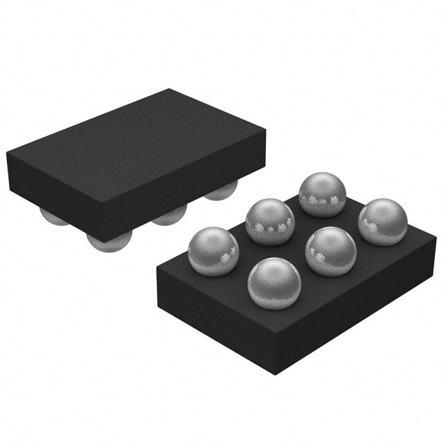
GENERIC PACKAGE VIEW DRV 6 WSON - 0.8 mm max height PLASTIC SMALL OUTLINE - NO LEAD Images above are just a representation of the package family, actual package may vary. Refer to the product data sheet for package details. 4206925/F
PACKAGE OUTLINE DRV0006A WSON - 0.8 mm max height SCALE 5.500 PLASTIC SMALL OUTLINE - NO LEAD B 2.1 A 1.9 PIN 1 INDEX AREA 2.1 1.9 0.8 C 0.7 SEATING PLANE 0.08 C (0.2) TYP 1 0.1 0.05 EXPOSED 0.00 THERMAL PAD 3 4 2X 7 1.3 1.6 0.1 6 1 4X 0.65 0.35 6X PIN 1 ID 0.3 0.25 6X (OPTIONAL) 0.2 0.1 C A B 0.05 C 4222173/B 04/2018 NOTES: 1. All linear dimensions are in millimeters. Any dimensions in parenthesis are for reference only. Dimensioning and tolerancing per ASME Y14.5M. 2. This drawing is subject to change without notice. 3. The package thermal pad must be soldered to the printed circuit board for thermal and mechanical performance. www.ti.com
EXAMPLE BOARD LAYOUT DRV0006A WSON - 0.8 mm max height PLASTIC SMALL OUTLINE - NO LEAD 6X (0.45) (1) 1 7 6X (0.3) 6 SYMM (1.6) (1.1) 4X (0.65) 4 3 (R0.05) TYP SYMM ( 0.2) VIA (1.95) TYP LAND PATTERN EXAMPLE SCALE:25X 0.07 MAX 0.07 MIN ALL AROUND ALL AROUND SOLDER MASK METAL METAL UNDER SOLDER MASK OPENING SOLDER MASK OPENING NON SOLDER MASK DEFINED SOLDER MASK (PREFERRED) DEFINED SOLDER MASK DETAILS 4222173/B 04/2018 NOTES: (continued) 4. This package is designed to be soldered to a thermal pad on the board. For more information, see Texas Instruments literature number SLUA271 (www.ti.com/lit/slua271). 5. Vias are optional depending on application, refer to device data sheet. If some or all are implemented, recommended via locations are shown. www.ti.com
EXAMPLE STENCIL DESIGN DRV0006A WSON - 0.8 mm max height PLASTIC SMALL OUTLINE - NO LEAD SYMM 6X (0.45) METAL 1 7 6X (0.3) 6 (0.45) SYMM 4X (0.65) (0.7) 4 3 (R0.05) TYP (1) (1.95) SOLDER PASTE EXAMPLE BASED ON 0.125 mm THICK STENCIL EXPOSED PAD #7 88% PRINTED SOLDER COVERAGE BY AREA UNDER PACKAGE SCALE:30X 4222173/B 04/2018 NOTES: (continued) 6. Laser cutting apertures with trapezoidal walls and rounded corners may offer better paste release. IPC-7525 may have alternate design recommendations. www.ti.com
PACKAGE OUTLINE DRV0006D WSON - 0.8 mm max height SCALE 5.500 PLASTIC SMALL OUTLINE - NO LEAD B 2.1 A 1.9 PIN 1 INDEX AREA 2.1 1.9 0.8 C 0.7 SEATING PLANE 0.08 C (0.2) TYP 1 0.1 0.05 EXPOSED 0.00 THERMAL PAD 3 4 2X 7 1.3 1.6 0.1 6 1 4X 0.65 0.35 6X PIN 1 ID 0.3 0.25 6X (OPTIONAL) 0.2 0.1 C A B 0.05 C 4225563/A 12/2019 NOTES: 1. All linear dimensions are in millimeters. Any dimensions in parenthesis are for reference only. Dimensioning and tolerancing per ASME Y14.5M. 2. This drawing is subject to change without notice. 3. The package thermal pad must be soldered to the printed circuit board for thermal and mechanical performance. www.ti.com
EXAMPLE BOARD LAYOUT DRV0006D WSON - 0.8 mm max height PLASTIC SMALL OUTLINE - NO LEAD 6X (0.45) (1) 1 7 6X (0.3) 6 SYMM (1.6) (1.1) 4X (0.65) 4 3 (R0.05) TYP SYMM ( 0.2) VIA (1.95) TYP LAND PATTERN EXAMPLE EXPOSED METAL SHOWN SCALE:25X 0.07 MAX 0.07 MIN ALL AROUND ALL AROUND EXPOSED EXPOSED METAL METAL SOLDER MASK METAL METAL UNDER SOLDER MASK OPENING SOLDER MASK OPENING NON SOLDER MASK DEFINED SOLDER MASK (PREFERRED) DEFINED SOLDER MASK DETAILS 4225563/A 12/2019 NOTES: (continued) 4. This package is designed to be soldered to a thermal pad on the board. For more information, see Texas Instruments literature number SLUA271 (www.ti.com/lit/slua271). 5. Vias are optional depending on application, refer to device data sheet. If some or all are implemented, recommended via locations are shown. www.ti.com
EXAMPLE STENCIL DESIGN DRV0006D WSON - 0.8 mm max height PLASTIC SMALL OUTLINE - NO LEAD SYMM 6X (0.45) METAL 1 7 6X (0.3) 6 (0.45) SYMM 4X (0.65) (0.7) 4 3 (R0.05) TYP (1) (1.95) SOLDER PASTE EXAMPLE BASED ON 0.125 mm THICK STENCIL EXPOSED PAD #7 88% PRINTED SOLDER COVERAGE BY AREA UNDER PACKAGE SCALE:30X 4225563/A 12/2019 NOTES: (continued) 6. Laser cutting apertures with trapezoidal walls and rounded corners may offer better paste release. IPC-7525 may have alternate design recommendations. www.ti.com
IMPORTANTNOTICEANDDISCLAIMER TI PROVIDES TECHNICAL AND RELIABILITY DATA (INCLUDING DATASHEETS), DESIGN RESOURCES (INCLUDING REFERENCE DESIGNS), APPLICATION OR OTHER DESIGN ADVICE, WEB TOOLS, SAFETY INFORMATION, AND OTHER RESOURCES “AS IS” AND WITH ALL FAULTS, AND DISCLAIMS ALL WARRANTIES, EXPRESS AND IMPLIED, INCLUDING WITHOUT LIMITATION ANY IMPLIED WARRANTIES OF MERCHANTABILITY, FITNESS FOR A PARTICULAR PURPOSE OR NON-INFRINGEMENT OF THIRD PARTY INTELLECTUAL PROPERTY RIGHTS. These resources are intended for skilled developers designing with TI products. You are solely responsible for (1) selecting the appropriate TI products for your application, (2) designing, validating and testing your application, and (3) ensuring your application meets applicable standards, and any other safety, security, or other requirements. These resources are subject to change without notice. TI grants you permission to use these resources only for development of an application that uses the TI products described in the resource. Other reproduction and display of these resources is prohibited. No license is granted to any other TI intellectual property right or to any third party intellectual property right. TI disclaims responsibility for, and you will fully indemnify TI and its representatives against, any claims, damages, costs, losses, and liabilities arising out of your use of these resources. TI’s products are provided subject to TI’s Terms of Sale (www.ti.com/legal/termsofsale.html) or other applicable terms available either on ti.com or provided in conjunction with such TI products. TI’s provision of these resources does not expand or otherwise alter TI’s applicable warranties or warranty disclaimers for TI products. Mailing Address: Texas Instruments, Post Office Box 655303, Dallas, Texas 75265 Copyright © 2020, Texas Instruments Incorporated