ICGOO在线商城 > 集成电路(IC) > PMIC - 稳压器 - DC DC 开关稳压器 > TPS62151RGTT
 Datasheet下载
- 型号: TPS62151RGTT
- 制造商: Texas Instruments
- 库位|库存: xxxx|xxxx
- 要求:
| 数量阶梯 | 香港交货 | 国内含税 |
| +xxxx | $xxxx | ¥xxxx |
查看当月历史价格
查看今年历史价格
TPS62151RGTT产品简介:
ICGOO电子元器件商城为您提供TPS62151RGTT由Texas Instruments设计生产,在icgoo商城现货销售,并且可以通过原厂、代理商等渠道进行代购。 TPS62151RGTT价格参考。Texas InstrumentsTPS62151RGTT封装/规格:PMIC - 稳压器 - DC DC 开关稳压器, 固定 降压 开关稳压器 IC 正 1.8V 1 输出 1A 16-VFQFN 裸露焊盘。您可以下载TPS62151RGTT参考资料、Datasheet数据手册功能说明书,资料中有TPS62151RGTT 详细功能的应用电路图电压和使用方法及教程。
| 参数 | 数值 |
| 产品目录 | 集成电路 (IC)半导体 |
| 描述 | IC REG BUCK SYNC 1.8V 1A 16QFN稳压器—开关式稳压器 3-17V 1A SD Cnvrtr |
| 产品分类 | |
| 品牌 | Texas Instruments |
| 产品手册 | http://www.ti.com/lit/gpn/tps62151 |
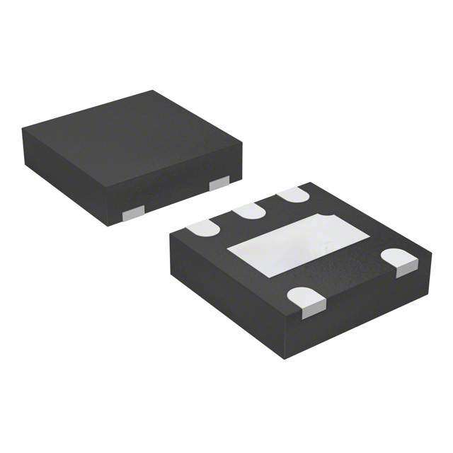
| 产品图片 |
|
| rohs | 符合RoHS无铅 / 符合限制有害物质指令(RoHS)规范要求 |
| 产品系列 | 电源管理 IC,稳压器—开关式稳压器,Texas Instruments TPS62151RGTTDCS-Control™ |
| 数据手册 | |
| 产品型号 | TPS62151RGTT |
| PCN设计/规格 | |
| PWM类型 | 混合物 |
| 产品种类 | 稳压器—开关式稳压器 |
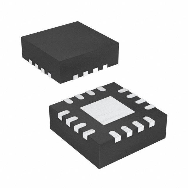
| 供应商器件封装 | 16-QFN(3x3) |
| 其它名称 | 296-30008-6 |
| 制造商产品页 | http://www.ti.com/general/docs/suppproductinfo.tsp?distId=10&orderablePartNumber=TPS62151RGTT |
| 包装 | Digi-Reel® |
| 同步整流器 | 是 |
| 商标 | Texas Instruments |
| 安装类型 | 表面贴装 |
| 安装风格 | SMD/SMT |
| 封装 | Reel |
| 封装/外壳 | 16-VFQFN 裸露焊盘 |
| 封装/箱体 | VQFN-16 |
| 工作温度 | -40°C ~ 85°C |
| 工作温度范围 | - 40 C to + 85 C |
| 工厂包装数量 | 250 |
| 开关频率 | 2.5 MHz |
| 拓扑结构 | Buck |
| 最大工作温度 | + 85 C |
| 最大输入电压 | 17 V |
| 最小工作温度 | - 40 C |
| 最小输入电压 | 3 V |
| 标准包装 | 1 |
| 电压-输入 | 3 V ~ 17 V |
| 电压-输出 | 1.8V |
| 电流-输出 | 1A |
| 类型 | 降压(降压) |
| 系列 | TPS62151 |
| 设计资源 | http://www.digikey.com/product-highlights/cn/zh/texas-instruments-webench-design-center/3176 |
| 输入电压 | 3 V to 17 V |
| 输出数 | 1 |
| 输出电压 | 1.8 V |
| 输出电流 | 1 A |
| 输出端数量 | 1 Output |
| 输出类型 | 固定 |
| 频率-开关 | 2.5MHz |


.jpg)


- 商务部:美国ITC正式对集成电路等产品启动337调查
- 曝三星4nm工艺存在良率问题 高通将骁龙8 Gen1或转产台积电
- 太阳诱电将投资9.5亿元在常州建新厂生产MLCC 预计2023年完工
- 英特尔发布欧洲新工厂建设计划 深化IDM 2.0 战略
- 台积电先进制程称霸业界 有大客户加持明年业绩稳了
- 达到5530亿美元!SIA预计今年全球半导体销售额将创下新高
- 英特尔拟将自动驾驶子公司Mobileye上市 估值或超500亿美元
- 三星加码芯片和SET,合并消费电子和移动部门,撤换高东真等 CEO
- 三星电子宣布重大人事变动 还合并消费电子和移动部门
- 海关总署:前11个月进口集成电路产品价值2.52万亿元 增长14.8%


PDF Datasheet 数据手册内容提取
Product Order Technical Tools & Support & Reference Folder Now Documents Software Community Design TPS62150,TPS62150A,TPS62151,TPS62152,TPS62153 SLVSAL5D–NOVEMBER2011–REVISEDSEPTEMBER2016 TPS6215x 3-V to 17-V, 1-A Step-Down Converter in 3-mm × 3-mm QFN Package 1 Features 3 Description • DCS-Control™Topology The TPS6215x family is an easy-to-use synchronous 1 step down dc-dc converter optimized for applications • InputVoltageRange:3Vto17V with high power density. A high switching frequency • Upto1-AOutputCurrent of typically 2.5 MHz allows the use of small inductors • AdjustableOutputVoltageFrom0.9Vto6V and provides fast transient response as well as high output-voltage accuracy by the use of DCS-Control • Pin-SelectableOutputVoltage(nominal,+5%) topology. • ProgrammableSoftStartandTracking With their wide operating input-voltage range of 3 V • SeamlessPower-SaveModeTransition to 17 V, the devices are ideally suited for systems • QuiescentCurrentof17 µA(typ.) powered from either Li-Ion or other batteries as well • SelectableOperatingFrequency as from 12-V intermediate power rails. The devices support up to 1-A continuous output current at output • Power-GoodOutput voltages between 0.9 V and 6 V (in 100% duty-cycle • 100%Duty-CycleMode mode). The soft-start pin controls the output-voltage • Short-CircuitProtection start-up ramp, which allows operation as either a • OvertemperatureProtection standalonepowersupplyorintrackingconfigurations. Power sequencing is also possible by configuring the • PintoPinCompatiblewithTPS62130and enable(EN)andopen-drainpower-good(PG)pins. TPS62140 In power-save mode, the devices draw quiescent • Availableina3-mm× 3-mm,VQFN-16Package current of about 17 μA from VIN. Power-save-mode, entered automatically and seamlessly if the load is 2 Applications small, maintains high efficiency over the entire load • Standard12-VRailSupplies range. In shutdown mode, the device turns off and currentconsumptionislessthan2μA. • POLSupplyFromSingleorMultipleLi-IonBattery • Solid-StateDiskDrives The device, available in adjustable- and fixed-output- voltage versions, comes in a 16-pin VQFN package • EmbeddedSystems measuring3×3mm(RGT). • LDOReplacement • MobilePCs,Tablets,Modems,Cameras DeviceInformation(1) • Server,Microserver PARTNUMBER PACKAGE BODYSIZE(NOM) • DataTerminal,PointofSales(ePOS) TPS6215X VQFN(16) 3.00mm×3.00mm (1) For all available packages, see the orderable addendum at theendofthedatasheet. TypicalApplicationSchematic EfficiencyvsOutputCurrent (3..17)V 2.2mH 1.8V/1A 100 PVIN SW AVIN VOS 100k 90 10mF EN PG 22mF SS/TRTPS62151 FB %) 80 VIN=5V VIN=12V VIN=17V 3.3nF y ( DEF AGND nc 70 e FSW PGND Effici 60 Copyright © 2016,Texas Instruments Incorporated 50 VOUT=3.3V fsw=1.25MHz 40 0.0 0.2 0.4 0.6 0.8 1.0 Output Current (A) G001 1 An IMPORTANT NOTICE at the end of this data sheet addresses availability, warranty, changes, use in safety-critical applications, intellectualpropertymattersandotherimportantdisclaimers.PRODUCTIONDATA.
TPS62150,TPS62150A,TPS62151,TPS62152,TPS62153 SLVSAL5D–NOVEMBER2011–REVISEDSEPTEMBER2016 www.ti.com Table of Contents 1 Features.................................................................. 1 9.1 ApplicationInformation............................................13 2 Applications........................................................... 1 9.2 TypicalApplication..................................................13 3 Description............................................................. 1 9.3 SystemExamples...................................................25 4 RevisionHistory..................................................... 2 10 PowerSupplyRecommendations..................... 28 5 DeviceComparisonTable..................................... 4 11 Layout................................................................... 29 11.1 LayoutGuidelines.................................................29 6 PinConfigurationandFunctions......................... 4 11.2 LayoutExample....................................................29 7 Specifications......................................................... 5 11.3 ThermalConsiderations........................................30 7.1 AbsoluteMaximumRatings......................................5 12 DeviceandDocumentationSupport................. 31 7.2 ESDRatings ............................................................5 12.1 DeviceSupport......................................................31 7.3 RecommendedOperatingConditions.......................5 12.2 DocumentationSupport........................................31 7.4 ThermalInformation..................................................5 12.3 RelatedLinks........................................................31 7.5 ElectricalCharacteristics...........................................6 12.4 ReceivingNotificationofDocumentationUpdates31 7.6 TypicalCharacteristics..............................................7 12.5 CommunityResources..........................................32 8 DetailedDescription.............................................. 8 12.6 Trademarks...........................................................32 8.1 Overview...................................................................8 12.7 ElectrostaticDischargeCaution............................32 8.2 FunctionalBlockDiagrams.......................................8 12.8 Glossary................................................................32 8.3 FeatureDescription...................................................9 13 Mechanical,Packaging,andOrderable 8.4 DeviceFunctionalModes........................................11 Information........................................................... 32 9 ApplicationandImplementation........................ 13 4 Revision History NOTE:Pagenumbersforpreviousrevisionsmaydifferfrompagenumbersinthecurrentversion. ChangesfromRevisionC(November2014)toRevisionD Page • Added"PintoPinCompatiblewithTPS62130andTPS62140"toFeatureslist .................................................................. 1 • ChangedtheT MAXvalueFrom:125°CTo:150°CintheAbsoluteMaximumRating ....................................................... 5 J • ChangedtheThermalInformationvalues ............................................................................................................................. 5 • Changed(T =–40°Cto85°C)To:(T =–40°Cto125°C)intheElectricalCharacteristicsconditions ............................... 6 J J • AddedatestconditionforIQatTA=-40°Cto+85°CintheElectricalCharacteristics ........................................................ 6 • AddedTable1andTable2 ................................................................................................................................................. 10 • Addedindicators(C1,C3,andC5)forcapacitancestoFigure7......................................................................................... 13 • AddedSwitchingFrequencygraphsfor1.0-V,1.8-V,and5.0-Vapplications(Figure24throughFigure31) ....................20 • ChangedLayoutExample ................................................................................................................................................... 29 ChangesfromRevisionB(June2013)toRevisionC Page • AddedDeviceandDocumentationSupportsection,LayoutandESDRatingstable............................................................ 1 ChangesfromRevisionA(November2012)toRevisionB Page • AddeddeviceTPS62150Atodatasheet............................................................................................................................... 1 • AddedtexttoTrackingFunctionsectionforclarification...................................................................................................... 17 2 SubmitDocumentationFeedback Copyright©2011–2016,TexasInstrumentsIncorporated ProductFolderLinks:TPS62150 TPS62150A TPS62151 TPS62152 TPS62153
TPS62150,TPS62150A,TPS62151,TPS62152,TPS62153 www.ti.com SLVSAL5D–NOVEMBER2011–REVISEDSEPTEMBER2016 ChangesfromOriginal(November2011)toRevisionA Page • AddedvaluestotheInitialoutputvoltageaccuracyforTA=–10°Cto85°C......................................................................... 6 • Power-SaveModeOperationsectionfollowingEquation1................................................................................................. 11 • ChangedtheLayoutGuidelinessection............................................................................................................................... 29 • ChangedLayoutExample.................................................................................................................................................... 29 Copyright©2011–2016,TexasInstrumentsIncorporated SubmitDocumentationFeedback 3 ProductFolderLinks:TPS62150 TPS62150A TPS62151 TPS62152 TPS62153
TPS62150,TPS62150A,TPS62151,TPS62152,TPS62153 SLVSAL5D–NOVEMBER2011–REVISEDSEPTEMBER2016 www.ti.com 5 Device Comparison Table PARTNUMBER OUTPUTVOLTAGE PowerGoodLogicLevel(EN=Low) TPS62150 adjustable HighImpedance TPS62150A adjustable Low TPS62151 1.8V HighImpedance TPS62152 3.3V HighImpedance TPS62153 5.0V HighImpedance 6 Pin Configuration and Functions RGTPackage 16-PinVQFNWithThermalPad TopView D D N N S G G O N P P V E 16 15 14 13 SW 1 12 PVIN SW 2 11 PVIN Exposed ThermalPad SW 3 10 AVIN PG 4 9 SS/TR 5 6 7 8 B D W F F GN FS DE A PinFunctions PIN(1) I/O DESCRIPTION NO. NAME 1,2,3 SW O Switchnode,whichisconnectedtotheinternalMOSFETswitches.ConnectinductorbetweenSWand outputcapacitor. 4 PG O Outputpowergood(High=V ready,Low=V belownominalregulation);opendrain(requires OUT OUT pull-upresistor) 5 FB I Voltagefeedbackofadjustableversion.Connectresistivevoltagedividertothispin.Itisrecommended toconnectFBtoAGNDonfixedoutputvoltageversionsforimprovedthermalperformance. 6 AGND AnalogGround.MustbeconnecteddirectlytotheExposedThermalPadandcommongroundplane. 7 FSW I SwitchingFrequencySelect(Low≈2.5MHz,High≈1.25MHz(2)fortypicaloperation)(3) 8 DEF I OutputVoltageScaling(Low=nominal,High=nominal+5%)(3) Soft-Start/TrackingPin.Anexternalcapacitorconnectedtothispinsetstheinternalvoltagereference 9 SS/TR I risetime.Itcanbeusedfortrackingandsequencing. 10 AVIN I Supplyvoltageforcontrolcircuitry.ConnecttosamesourceasPVIN. 11,12 PVIN I Supplyvoltageforpowerstage.ConnecttosamesourceasAVIN. 13 EN I Enableinput(High=enabled,Low=disabled)(3) 14 VOS I Outputvoltagesensepinandconnectionforthecontrolloopcircuitry. 15,16 PGND PowerGround.MustbeconnecteddirectlytotheExposedThermalPadandcommongroundplane. Exposed MustbeconnectedtoAGND(pin6),PGND(pin15,16)andcommongroundplane.SeetheLayout ThermalPad Example.Mustbesolderedtoachieveappropriatepowerdissipationandmechanicalreliability. (1) Formoreinformationaboutconnectingpins,seetheDetailedDescriptionandApplicationandImplementationsections. (2) ConnectFSWtoV orPGinthiscase. OUT (3) Aninternalpull-downresistorkeepslogiclevellow,ifpinisfloating. 4 SubmitDocumentationFeedback Copyright©2011–2016,TexasInstrumentsIncorporated ProductFolderLinks:TPS62150 TPS62150A TPS62151 TPS62152 TPS62153
TPS62150,TPS62150A,TPS62151,TPS62152,TPS62153 www.ti.com SLVSAL5D–NOVEMBER2011–REVISEDSEPTEMBER2016 7 Specifications 7.1 Absolute Maximum Ratings(1) overoperatingjunctiontemperaturerange(unlessotherwisenoted) MIN MAX UNIT AVIN,PVIN –0.3 20 EN,SS/TR –0.3 V +0.3 Pinvoltage(2) IN V SW –0.3 V +0.3 IN DEF,FSW,FB,PG,VOS –0.3 7 Power-goodsinkcurrent PG 10 mA Operatingjunctiontemperature,T –40 150 °C J Temperature Storagetemperature,T –65 150 °C stg (1) StressesbeyondthoselistedunderAbsoluteMaximumRatingsmaycausepermanentdamagetothedevice.Thesearestressratings only,andfunctionaloperationofthedeviceattheseoranyotherconditionsbeyondthoseindicatedunderRecommendedOperating Conditionsisnotimplied.Exposuretoabsolute-maximum-ratedconditionsforextendedperiodsmayaffectdevicereliability. (2) Allvoltagesarewithrespecttonetworkgroundterminal. 7.2 ESD Ratings VALUE UNIT Humanbodymodel(HBM),perANSI/ESDA/JEDECJS-001,all pins(1) ±2000 V V Electrostaticdischarge (ESD) Chargeddevicemodel(CDM),perJEDECspecification JESD22-C101,allpins(2) ±500 V (1) JEDECdocumentJEP155statesthat500-VHBMallowssafemanufacturingwithastandardESDcontrolprocess. (2) JEDECdocumentJEP157statesthat250-VCDMallowssafemanufacturingwithastandardESDcontrolprocess. 7.3 Recommended Operating Conditions overoperatingjunctiontemperaturerange(unlessotherwisenoted) MIN NOM MAX UNIT SupplyVoltage,V (atAVINandPVIN) 3 17 V IN Operatingjunctiontemperature,T –40 125 °C J 7.4 Thermal Information TPS6215x THERMALMETRIC(1) UNIT RGT16PINS R Junction-to-ambientthermalresistance 45 °C/W θJA R Junction-to-case(top)thermalresistance 53.6 °C/W θJC(top) R Junction-to-boardthermalresistance 17.4 °C/W θJB ψ Junction-to-topcharacterizationparameter 1.1 °C/W JT ψ Junction-to-boardcharacterizationparameter 17.4 °C/W JB R Junction-to-case(bottom)thermalresistance 4.5 °C/W θJC(bot) (1) Formoreinformationabouttraditionalandnewthermalmetrics,seetheSemiconductorandICPackageThermalMetricsapplication report. Copyright©2011–2016,TexasInstrumentsIncorporated SubmitDocumentationFeedback 5 ProductFolderLinks:TPS62150 TPS62150A TPS62151 TPS62152 TPS62153
TPS62150,TPS62150A,TPS62151,TPS62152,TPS62153 SLVSAL5D–NOVEMBER2011–REVISEDSEPTEMBER2016 www.ti.com 7.5 Electrical Characteristics overoperatingjunctiontemperature(T =-40°Cto125°C),typicalvaluesatVIN=12VandT =25°C(unlessotherwisenoted) J A PARAMETER TESTCONDITIONS MIN NOM MAX UNIT SUPPLY V InputVoltageRange(1) 3 17 V IN EN=High,I =0mA, 17 30 I OperatingQuiescentCurrent OUT µA Q devicenotswitching T =-40°Cto+85°C 17 25 A 1.5 25 I ShutdownCurrent(2) EN=Low µA SD T =-40°Cto+85°C 1.5 4 A FallingInputVoltage(PWMmodeoperation) 2.6 2.7 2.8 V V UndervoltageLockoutThreshold UVLO Hysteresis 200 mV ThermalShutdownTemperature 160 T °C SD ThermalShutdownHysteresis 20 CONTROL(EN,DEF,FSW,SS/TR,PG) HighLevelInputThresholdVoltage(EN, V 0.9 0.65 V H DEF,FSW) V LowLevelInputThresholdVoltage(EN, L 0.45 0.3 V DEF,FSW) I InputLeakageCurrent(EN,DEF,FSW) EN=V orGND;DEF,FSW=V orGND 0.01 1 µA LKG IN OUT Rising(%V ) 92% 95% 98% OUT V PowerGoodThresholdVoltage TH_PG Falling(%V ) 87% 90% 94% OUT V PowerGoodOutputLowVoltage I =–2mA 0.07 0.3 V OL_PG PG I InputLeakageCurrent(PG) V =1.8V 1 400 nA LKG_PG PG I SS/TRPinSourceCurrent 2.3 2.5 2.7 µA SS/TR POWERSWITCH V ≥6V 90 170 IN High-SideMOSFETON-Resistance mΩ V =3V 120 IN r DS(on) V ≥6V 40 70 IN Low-SideMOSFETON-Resistance mΩ V =3V 50 IN High-SideMOSFETForwardCurrent V =12V,T =25°C ILIMF Limit(3) IN A 1.4 1.7 2.2 A OUTPUT I InputLeakageCurrent(FB) TPS62150,V =0.8V 1 100 nA LKG_FB FB OutputVoltageRange(TPS62150) V ≥V 0.9 6.0 V IN OUT DEF=0(GND) V OUT DEF(OutputVoltageProgramming) DEF=1(V ) V +5% OUT OUT PWMmodeoperation,V ≥V +1V 785.6 800 814.4 IN OUT PWMmodeoperation,V ≥V +1V, VOUT InitialOutputVoltageAccuracy(4) TA=–10°Cto85°C IN OUT 788.0 800 812.8 mV PowerSaveModeoperation,C =22µF 781.6 800 822.4 OUT LoadRegulation(5) V =12V,V =3.3V,PWMmode IN OUT 0.05 %/A operation LineRegulation(5) 3V≤V ≤17V,V =3.3V,I =1A, IN OUT OUT 0.02 %/V PWMmodeoperation (1) ThedeviceisstillfunctionaldowntoUndervoltageLockout(seeparameterV ). UVLO (2) CurrentintoAVIN+PVINpins. (3) Thisisthestaticcurrentlimit.Itcanbetemporarilyhigherinapplicationsduetointernalpropagationdelay(seeCurrent-LimitandShort- CircuitProtectionsection). (4) ThisistheaccuracyprovidedattheFBpinfortheadjustableV version(lineandloadregulationeffectsarenotincluded).Forthe OUT fixedvoltageversionsthe(internal)resistivedividerisincluded. (5) Lineandloadregulationdependonexternalcomponentselectionandlayout(seeFigure22andFigure23). 6 SubmitDocumentationFeedback Copyright©2011–2016,TexasInstrumentsIncorporated ProductFolderLinks:TPS62150 TPS62150A TPS62151 TPS62152 TPS62153
TPS62150,TPS62150A,TPS62151,TPS62152,TPS62153 www.ti.com SLVSAL5D–NOVEMBER2011–REVISEDSEPTEMBER2016 7.6 Typical Characteristics Figure1.QuiescentCurrent Figure2.ShutdownCurrent 200 100 180 W) 160 125°C W) 80 e (m 140 85°C e (m 125°C d 120 d 60 85°C Si Si Son High− 1680000 −2150°C°C Son Low− 40 −2150°°CC D D R 40 −40°C R 20 −40°C 20 0 0 0 3 6 9 12 15 18 20 0 3 6 9 12 15 18 20 Input Voltage (V) Input Voltage (V) Figure3.High-SideSwitchResistance Figure4.Low-SideSwitchResistance Copyright©2011–2016,TexasInstrumentsIncorporated SubmitDocumentationFeedback 7 ProductFolderLinks:TPS62150 TPS62150A TPS62151 TPS62152 TPS62153
TPS62150,TPS62150A,TPS62151,TPS62152,TPS62153 SLVSAL5D–NOVEMBER2011–REVISEDSEPTEMBER2016 www.ti.com 8 Detailed Description 8.1 Overview The TPS6215x synchronous switched-mode power converter is based on DCS-Control topology, an advanced regulation topology that combines the advantages of hysteretic, voltage-mode, and current-mode control, including an ac loop directly associated with the output voltage. This control loop takes information about output voltage changes and feeds that information directly to a fast comparator stage. It sets the switching frequency, which is constant for steady-state operating conditions, and provides immediate response to dynamic load changes. To get accurate dc load regulation, a voltage feedback loop is used. The internally compensated regulationnetworkachievesfastandstableoperationwithsmallexternalcomponentsandlow-ESRcapacitors. The DCS-Control topology supports pulse-width modulation (PWM) mode for medium and heavy load conditions and a power-save mode at light loads. During PWM, it operates at its nominal switching frequency in continuous- conduction mode. This frequency is typically about 2.5 MHz or 1.25 MHz, with a controlled frequency variation depending on the input voltage. If the load current decreases, the converter enters power-save mode to sustain high efficiency down to very light loads. In power-save mode, the switching frequency decreases linearly with the load current. Because DCS-Control topology supports both operation modes within a single building block, the transitionfromPWMtopower-savemodeisseamlesswithouteffectsontheoutputvoltage. Fixed-output voltage versions provide the smallest solution size and lowest current consumption, requiring only threeexternalcomponents.Aninternalcurrentlimitsupportsnominaloutputcurrentsofupto1A. The TPS6215x offers both excellent dc voltage and superior load transient regulation, combined with very low outputvoltageripple,minimizinginterferencewithRFcircuits. 8.2 Functional Block Diagrams PG AVIN PVIN PVIN Soft Thermal UVLO PGcontrol start Shtdwn HSlim comp EN* SW SS/TR power gate controllogic control drive SW DEF* SW FSW* comp LSlim VOS directcontrol & ramp compensation _ FB comparator timertON error + amplifier DCS-ControlTM AGND PGNDPGND Copyright © 2016,Texas Instruments Incorporated *Thispinisconnectedtoapulldownresistorinternally(seeFeatureDescriptionsection) Figure5. TPS62150(AdjustableOutputVoltage) 8 SubmitDocumentationFeedback Copyright©2011–2016,TexasInstrumentsIncorporated ProductFolderLinks:TPS62150 TPS62150A TPS62151 TPS62152 TPS62153
TPS62150,TPS62150A,TPS62151,TPS62152,TPS62153 www.ti.com SLVSAL5D–NOVEMBER2011–REVISEDSEPTEMBER2016 Functional Block Diagrams (continued) PG AVIN PVIN PVIN Soft Thermal UVLO PGcontrol start Shtdwn HSlim comp EN* SW SS/TR power gate controllogic control drive SW DEF* SW FSW* comp LSlim VOS directcontrol & ramp compensation _ FB* comparator timertON error + amplifier DCS-ControlTM AGND PGNDPGND Copyright © 2016,Texas Instruments Incorporated *Thispinisconnectedtoapulldownresistorinternally(seeFeatureDescriptionsection) Figure6. TPS62151,-2,-3(FixedOutputVoltage) 8.3 Feature Description 8.3.1 Enable/Shutdown(EN) When Enable (EN) is set High, the device starts operation. Shutdown is forced if EN is pulled Low with a shutdown current of typically 1.5µA. During shutdown, the internal power MOSFETs as well as the entire control circuitry are turned off. The internal resistive divider pulls down the output voltage smoothly. The EN signal must be set externally to High or Low. An internal pull-down resistor of about 400kΩ is connected and keeps EN logic low,ifLowissetinitiallyandthenthepingetsfloating.ItisdisconnectedifthepinissetHigh Connecting the EN pin to an appropriate output signal of another power rail provides sequencing of multiple powerrails. 8.3.2 Soft-StartorTracking(SS/TR) The internal soft-start circuitry controls the output voltage slope during start-up. This avoids excessive inrush current and ensures a controlled output-voltage rise time. It also prevents unwanted voltage drops from high- impedance power sources or batteries. When EN is set to start device operation, the device starts switching after a delay of about 50 µs, and V rises with a slope controlled by an external capacitor connected to the SS/TR OUT pin.SeeFigure40andFigure41fortypicalstart-upoperation. Copyright©2011–2016,TexasInstrumentsIncorporated SubmitDocumentationFeedback 9 ProductFolderLinks:TPS62150 TPS62150A TPS62151 TPS62152 TPS62153
TPS62150,TPS62150A,TPS62151,TPS62152,TPS62153 SLVSAL5D–NOVEMBER2011–REVISEDSEPTEMBER2016 www.ti.com Feature Description (continued) Using a very small capacitor (or leaving the SS/TR pin disconnected) provides fastest start-up behavior. There is no theoretical limit for the longest startup time. The TPS6215x can start into a pre-biased output. During monotonic pre-biased start-up, both the power MOSFETs are not allowed to turn on until the internal ramp of the device sets an output voltage above the pre-bias voltage. If the device is set to shutdown (EN = GND), undervoltage lockout, or thermal shutdown, an internal resistor pulls the SS/TR pin down to ensure a proper low level.Returningfromthosestatescausesanewstart-upsequenceassetbytheSS/TRconnection. A voltage supplied to SS/TR can be used for tracking a master voltage. The output voltage follows this voltage in bothdirections,upanddown(seeApplicationandImplementation). 8.3.3 PowerGood(PG) The TPS6215x has a built-in power-good (PG) function to indicate whether the output voltage has reached its appropriate level or not. One use of the PG signal can be for start-up sequencing of multiple rails. The PG pin is an open-drain output that requires a pullup resistor (to any voltage below 7 V). It can sink 2 mA of current and maintain its specified logic-low level. With TPS62150 it it is high impedance when the device is turned off due to EN, UVLO or thermal shutdown. TPS62150A features PG=Low in this case and can be used to actively discharge V (see Figure 45). VIN must remain present for the PG pin to stay Low. See SLVA644 for OUT applicationdetails.Ifnotused,thePGpinshouldbeconnectedtoGNDbutmaybeleftfloating. space Table1.PowerGoodPinLogicTable(TPS62150) PGLogicStatus DeviceState HighImpedance Low V ≥V √ FB TH_PG Enable(EN=High) V ≤V √ FB TH_PG Shutdown(EN=Low) √ UVLO 0.7V<V <V √ IN UVLO ThermalShutdown T >T √ J SD PowerSupplyRemoval V <0.7V √ IN space Table2.PowerGoodPinLogicTable(TPS62150A) PGLogicStatus DeviceState HighImpedance Low V ≥V √ FB TH_PG Enable(EN=High) V ≤V √ FB TH_PG Shutdown(EN=Low) √ UVLO 0.7V<V <V √ IN UVLO ThermalShutdown T >T √ J SD PowerSupplyRemoval V <0.7V √ IN space 8.3.4 Pin-SelectableOutputVoltage(DEF) Setting the DEF pin to High increases the output voltage of the TPS62150x devices by 5% above the nominal voltage (1). When DEF is Low, the device regulates to the nominal output voltage. Increasing the nominal voltage allows adapting the power supply voltage to the variations of the application hardware. More detailed information on voltage margining using the TPS62150x device is in SLVA489. The pin has an internally connected pulldown resistorofabout400kΩtoensureaproperlogiclevelifthepinishigh-impedanceorfloatingafteraninitiallyLow setting.SettingthepinHighdisconnectstheresistor. (1) Maximumallowedvoltageis7V.Therefore,therecommendedconnectionforDEFistoV ,notV . OUT IN 10 SubmitDocumentationFeedback Copyright©2011–2016,TexasInstrumentsIncorporated ProductFolderLinks:TPS62150 TPS62150A TPS62151 TPS62152 TPS62153
TPS62150,TPS62150A,TPS62151,TPS62152,TPS62153 www.ti.com SLVSAL5D–NOVEMBER2011–REVISEDSEPTEMBER2016 8.3.5 FrequencySelection(FSW) To get high power density with a very small solution size, a high switching frequency allows the use of small external components for the output filter. However, switching losses increase with the switching frequency. If efficiency is the key parameter, more than solution size, the switching frequency can be set to half (1.25 MHz typical) by pulling FSW to High. It is mandatory to start with FSW = Low to limit inrush current, which connecting FSW to V or PG can accomplish. Running with lower frequency produces higher efficiency, but also creates OUT higher output-voltage ripple. Pull FSW to Low for high-frequency operation (2.5 MHz typical). To get low ripple and full output current at the lower switching frequency, the recommended minimum inductor value is 2.2 µH. An application can change the switching frequency during operation, if needed. An internally connected pulldown resistor of about 400 kΩ on this pin acts the same way as one on the DEF pin (see Pin-Selectable Output Voltage(DEF)). 8.3.6 UndervoltageLockout(UVLO) If the input voltage drops, the undervoltage lockout prevents faulty operation of the device by switching off both the power FETs. The typical undervoltage-lockout threshold setting is 2.7 V. The device is fully operational for voltages above the UVLO threshold and turns off if the input voltage trips the threshold. The converter starts operationagainoncetheinputvoltageexceedsthethresholdbyahysteresisoftypically200mV. 8.3.7 ThermalShutdown An internal temperature sensor monitors the junction temperature (T ) of the device. If T exceeds 160°C (typ), J J the device goes into thermal shutdown. Both the high-side and low-side power FETs turn off and PG goes into the high-impedance state. When T decreases below the hysteresis level, the converter resumes normal J operation, beginning with soft start. To avoid unstable conditions, the device implements a hysteresis of typically 20°Conthethermalshutdowntemperature. 8.4 Device Functional Modes 8.4.1 Pulse-WidthModulation(PWM)Operation The TPS6215x operates using pulse-width modulation in continuous-conduction mode (CCM) with a nominal switching frequency of 2.5 MHz or 1.25 MHz, selectable with the FSW pin. The frequency variation in the PWM mode is controlled and depends on V , V , and the inductance. The device operates in PWM mode as long IN OUT the output current is higher than half the inductor ripple current. To maintain high efficiency at light loads, the device enters power-save mode at the boundary of discontinuous conduction mode (DCM). This happens if the outputcurrentbecomessmallerthanhalftheinductorripplecurrent. 8.4.2 Power-SaveModeOperation The TPS6215x enters its built-in power-save mode seamlessly if the load current decreases. This secures a high efficiency in light load operation. The device remains in power-save mode as long as the inductor current is discontinuous. In power-save mode, the switching frequency decreases linearly with the load current, maintaining high efficiency. The transition into and out of power-save mode happens within the entire regulation scheme and is seamlessinbothdirections. TPS6215x includes a fixed on-time circuitry. An estimate for this on-time, in steady-state operation with FSW=Low,is: space V t = OUT ´400ns ON V IN (1) space For very small output voltages, an absolute minimum on-time of about 80 ns is kept to limit switching losses. The operatingfrequencyistherebyreducedfromitsnominalvalue,whichkeepsefficiencyhigh.Also,theoff-timecan reach its minimum value at high duty cycles. The output voltage remains regulated in such cases. Using t , the ON typicalpeakinductorcurrentinpower-savemodeisapproximatedby: space Copyright©2011–2016,TexasInstrumentsIncorporated SubmitDocumentationFeedback 11 ProductFolderLinks:TPS62150 TPS62150A TPS62151 TPS62152 TPS62153
TPS62150,TPS62150A,TPS62151,TPS62152,TPS62153 SLVSAL5D–NOVEMBER2011–REVISEDSEPTEMBER2016 www.ti.com Device Functional Modes (continued) (V -V ) I = IN OUT ´t LPSM(peak) ON L (2) space When V decreases to typically 15% above V , the TPS62150x device does not enter power-save mode, IN OUT regardlessoftheloadcurrent.ThedevicemaintainsoutputregulationinPWMmode. 8.4.3 100%Duty-CycleOperation The duty cycle of the buck converter is given by D = V / V and increases as the input voltage comes close OUT IN to the output voltage. In this case, the device starts 100% duty cycle operation turning on the high-side switch 100% of the time. The high-side switch stays turned on as long as the output voltage is below the internal set point. This allows the conversion of small input-to-output voltage differences, for example, for longest operation timeofbattery-poweredapplications.In100%dutycyclemode,thelow-sideFETisswitchedoff. The minimum input voltage to maintain output voltage regulation, depending on the load current and the output voltagelevel,iscalculatedas: spacing ( ) V = V +I ´ R + R IN(min) OUT(min) OUT DS(on) L where • I istheoutputcurrent OUT • R istheon-stateresistanceofthehigh-sideFET DS(on) • R isthedcresistanceoftheinductor (3) L 8.4.4 Current-LimitandShort-CircuitProtection The TPS6215x devices have protection against heavy-load and short-circuit events. At heavy loads, the current limit determines the maximum output current. If the current limit is reached, the high-side FET is turned off. Avoiding shoot-through current, then the low-side FET switches on to allow the inductor current to decrease. The low-side current limit is typically 1.2 A. The high-side FET turns on again only if the current in the low-side FET hasdecreasedbelowthelow-sidecurrent-limitthreshold. The output current of the device is limited by the current limit (see Electrical Characteristics). Due to internal propagation delay, the actual current can exceed the static current limit during that time. The dynamic current limitiscalculatedasfollows: spacing V I = I + L ´t peak(typ) LIMF PD L where • I isthestaticcurrentlimit,specifiedintheElectricalCharacteristics LIMF • V isthevoltageacrosstheinductor(V –V ) L IN OUT • Listheinductorvalue • t istheinternalpropagationdelay (4) PD space The current limit can exceed static values, especially if the input voltage is high and the application uses very smallinductances.Calculatethepeakcurrentinthedynamichigh-sideswitchusingthefollowingequation: space ( ) V -V IN OUT I = I + ´30ns peak(typ) LIMF L (5) 12 SubmitDocumentationFeedback Copyright©2011–2016,TexasInstrumentsIncorporated ProductFolderLinks:TPS62150 TPS62150A TPS62151 TPS62152 TPS62153
TPS62150,TPS62150A,TPS62151,TPS62152,TPS62153 www.ti.com SLVSAL5D–NOVEMBER2011–REVISEDSEPTEMBER2016 9 Application and Implementation NOTE Information in the following applications sections is not part of the TI component specification, and TI does not warrant its accuracy or completeness. TI’s customers are responsible for determining suitability of components for their purposes. Customers should validateandtesttheirdesignimplementationtoconfirmsystemfunctionality. 9.1 Application Information The TPS6215x devices are a switched-mode step-down converters, able to convert a 3-V to 17-V input voltage into a 0.9-V to 6-V output voltage, providing up to 1 A. They require a minimum number of external components. Apart from the LC output filter and the input capacitors, only the TPS62150 device needs an additional resistive dividertosettheoutputvoltagelevel. 9.2 Typical Application space (3..17)V 2.2µH VOUT/1A PVIN SW AVIN VOS 100k C1 C3 EN PG R1 10uF 22uF TPS62150 SS/TR FB C5 DEF AGND R2 3.3nF FSW PGND Copyright © 2016,Texas Instruments Incorporated Figure7. ATypical1-AStep-DownConverter space 9.2.1 DesignRequirements The following design guideline provides a component selection to operate the device within the recommended operating conditions. Using the FSW pin, the design can be optimized for highest efficiency or smallest solution size and lowest output-voltage ripple. For highest efficiency set FSW = High, and the device operates at the lower switching frequency. For smallest solution size and lowest output voltage ripple set FSW = Low, and the device operates with higher switching frequency. The typical values for all measurements are V = 12 V, V = IN OUT 3.3V,andT=25°C,usingtheexternalcomponentsofTable3. Thecomponentselectionusedformeasurementsisgivenasfollows: Table3.ListofComponents REFERENCE DESCRIPTION MANUFACTURER(1) IC 17-V,1-Astep-downconverter,QFN TPS62150RGT,TexasInstruments L1 2.2-µH,3.1-A,0.165-in×0.165-in(4.19-mm×4.19-mm) XFL4020-222MEB,Coilcraft C1 10-µF,25-V,ceramic,1210 Standard C3 22-µF,6.3-V,ceramic,0805 Standard C5 3300-pF,25-V,ceramic,0603 R1 DependingonV OUT R2 DependingonV OUT R3 100-kΩ,chip,0603,1/16-W,1% Standard (1) SeeThird-PartyProductsDisclaimer Copyright©2011–2016,TexasInstrumentsIncorporated SubmitDocumentationFeedback 13 ProductFolderLinks:TPS62150 TPS62150A TPS62151 TPS62152 TPS62153
TPS62150,TPS62150A,TPS62151,TPS62152,TPS62153 SLVSAL5D–NOVEMBER2011–REVISEDSEPTEMBER2016 www.ti.com 9.2.2 DetailedDesignProcedure 9.2.2.1 ProgrammingtheOutputVoltage Whereas the output voltage of the TPS62150 (TPS62150A) is adjustable, the TPS62151, -2, and -3 are programmed to fixed output voltages. For fixed output versions, the FB pin is pulled down internally and may be left floating. It is recommended to connect the FB pin to AGND to decrease thermal resistance. The adjustable version can be programmed for output voltages from 0.9 V to 6 V by using a resistive divider from V to OUT AGND. The voltage at the FB pin is regulated to 800 mV. The value of the output voltage is set by the selection of the resistive divider from Equation 6. It is recommended to choose resistor values which allow a current of at least 2 µA, meaning the value of R2 should not exceed 400 kΩ. Lower resistor values are recommended for highest accuracy and most robust design. For applications requiring lowest current consumption, the use of fixed-output-voltageversionsisrecommended. space æV ö R = R ´ ç OUT -1÷ 1 2 çV ÷ è REF ø (6) IncaseofanopenontheFBpin,thedeviceclampstheoutputvoltageattheVOSpininternallytoabout7.4V. 9.2.2.2 ExternalComponentSelection The external components must fulfill the needs of the application, but also the stability criteria for the control loop of the device. The TPS6215x device is optimized to work within a range of external components. Consider the inductance and capacitance of the LC output filters in conjunction, creating the double pole responsible for the corner frequency of the converter (see the Output Filter and Loop Stability section). Table 4 can be used to simplify the output filter component selection. Checked cells represent combinations that are proven for stability by simulation and lab test. Further combinations should be checked for each individual application. See SLVA463fordetails. Table4.L-COutputFilterCombinations(1) 4.7µF 10µF 22µF 47µF 100µF 200µF 400µF 0.47µH 1µH √ √ √ √ 2.2µH √ √(2) √ √ √ 3.3µH √ √ √ √ 4.7µH (1) Thevaluesinthetablearenominalvalues.Theeffectivecapacitancewasconsideredtovaryby+20%and-50%. (2) ThisLCcombinationisthestandardvalue,andisrecommendedformostapplications. spacing The TPS6215x device can operate with an inductor as low as 1 µH or 2.2 µH. FSW should be set Low in this case. However, for applications running with the low-frequency setting (FSW = High) or with low input voltages, 3.3 µHisrecommended. 9.2.2.2.1 InductorSelection The inductor selection is affected by several effects like inductor ripple current, output ripple voltage, PWM-to- PSM transition point, and efficiency. In addition, the inductor selected must be rated for appropriate saturation current and dc resistance (DCR). Equation 7 and Equation 8 calculate the maximum inductor current under static loadconditions. spacing DI I = I + L(max) L(max) OUT(max) 2 (7) space 14 SubmitDocumentationFeedback Copyright©2011–2016,TexasInstrumentsIncorporated ProductFolderLinks:TPS62150 TPS62150A TPS62151 TPS62152 TPS62153
TPS62150,TPS62150A,TPS62151,TPS62152,TPS62153 www.ti.com SLVSAL5D–NOVEMBER2011–REVISEDSEPTEMBER2016 æ V ö ç1- OUT ÷ V DI = V ´ ç IN(max) ÷ L(max) OUT çL ´f ÷ ç (min) SW ÷ ç ÷ è ø where • I (max)isthemaximuminductorcurrent L • ΔI isthepeak-to-peakinductorripplecurrent L • L(min)istheminimumeffectiveinductorvalue • f istheactualPWMswitchingfrequency (8) SW spacing Calculating the maximum inductor current using the actual operating conditions gives the minimum required saturation current of the inductor. An added margin of about 20% is recommended. A larger inductor value is also useful to get lower ripple current, but increases the transient response time and size as well. The following inductorshavebeenusedwiththeTPS6215xdeviceandarerecommendedforuse: Table5.ListofInductors TYPE INDUCTANCE[µH] SATURATION DIMENSIONS MANUFACTURER(2) CURRENT[A](1) [L×W×H],mm XFL4020-222ME_ 2.2µH,±20% 3.5 4×4×2.1 Coilcraft XFL3012-222MEC 2.2µH,±20% 1.6 3×3×1.2 Coilcraft XFL3012-332MEC 3.3µH,±20% 1.4 3×3×1.2 Coilcraft VLS252012T-2R2M1R3 2.2µH,±20% 1.3 2.5×2×1.2 TDK LPS3015-332 3.3µH,±20% 1.4 3×3×1.4 Coilcraft 744025003 3.3µH,±20% 1.5 2.8×2.8×2.8 Wuerth PSI25201B-2R2MS 2.2µH,±20% 1.3 2×2.5×1.2 Cyntec NR3015T-2R2M 2.2µH,±20% 1.5 3×3×1.5 TaiyoYuden (1) LowerofI at40°CriseorI at30%drop. RMS SAT (2) SeeThird-PartyProductsDisclaimer spacing Theinductorvaluealsodeterminestheloadcurrentatwhichthedeviceenterspower-savemode: space 1 I = DI load(PSM) L 2 (9) space UsingEquation8,thiscurrentlevelcanbeadjustedbychangingtheinductorvalue. 9.2.2.2.2 CapacitorSelection 9.2.2.2.2.1 OutputCapacitor The recommended value for the output capacitor is 22 µF. The architecture of the TPS6215x device allows the use of tiny ceramic output capacitors with low equivalent series resistance (ESR). These capacitors provide low output-voltage ripple and are recommended. To keep its low resistance up to high frequencies and to get narrow capacitance variation with temperature, it is recommended to use X7R or X5R dielectric. Using a higher value of output capacitance can have some advantages, like smaller voltage ripple and a tighter dc output accuracy in power-savemode(seeSLVA463). Note: In power-save mode, the output-voltage ripple depends on the output capacitance, the ESR of the output capacitor,andthepeakinductorcurrent.UsingceramiccapacitorsprovidessmallESRandlowripple. Copyright©2011–2016,TexasInstrumentsIncorporated SubmitDocumentationFeedback 15 ProductFolderLinks:TPS62150 TPS62150A TPS62151 TPS62152 TPS62153
TPS62150,TPS62150A,TPS62151,TPS62152,TPS62153 SLVSAL5D–NOVEMBER2011–REVISEDSEPTEMBER2016 www.ti.com 9.2.2.2.2.2 InputCapacitor For most applications, 10 µF is sufficient and is recommended, though a larger value reduces input-current ripple further. The input capacitor buffers the input voltage for transient events and also decouples the converter from the supply. A low-ESR multilayer ceramic capacitor is recommended for best filtering and should be placed between PVIN and PGND as close as possible to those pins. Even though AVIN and PVIN must be supplied from the same input source, it is recommended to place a capacitance of 0.1 µF from AVIN to AGND, to avoid potentialnoisecoupling.AnRC,low-passfilterfromPVINtoAVINmaybeusedbutisnotrequired. 9.2.2.2.2.3 Soft-StartCapacitor A capacitance connected between the SS/TR pin and AGND allows a user-programmable start-up slope of the output voltage. A constant-current source supplies 2.5 µA to charge the external capacitance. The capacitor requiredforagivensoft-startramptimefortheoutputvoltageisgivenby: space 2.5mA CSS=tSS´1.25 V éëFùû where • C isthecapacitance(F)requiredattheSS/TRpin SS • t isthedesiredsoft-startramptime(s) (10) SS spacing NOTE DC bias effect: High capacitance ceramic capacitors have a dc bias effect, which has a strong influence on the final effective capacitance. Therefore, selecting the right capacitor value requires careful choice. Package size and voltage rating in combination with dielectric material are responsible for differences between the rated capacitor value and theeffectivecapacitance. spacing 9.2.2.3 TrackingFunction If a tracking function is desired, the SS/TR pin can be used for this purpose by connecting it to an external tracking voltage. The output voltage tracks that voltage. If the tracking voltage is between 50 mV and 1.2 V, the FBpinwilltracktheSS/TRpinvoltageasdescribedinEquation11andshowninFigure8. spacing V »0.64´V FB SS/TR (11) spacing VSS/ TR[V] 1.2 0.8 0.4 0.2 0.4 0.6 0.8 VFB[V] Figure8. VoltageTrackingRelationship 16 SubmitDocumentationFeedback Copyright©2011–2016,TexasInstrumentsIncorporated ProductFolderLinks:TPS62150 TPS62150A TPS62151 TPS62152 TPS62153
TPS62150,TPS62150A,TPS62151,TPS62152,TPS62153 www.ti.com SLVSAL5D–NOVEMBER2011–REVISEDSEPTEMBER2016 OncetheSS/TRpinvoltagereachesabout1.2V,theinternalvoltageisclampedtotheinternalfeedbackvoltage and device goes to normal regulation. This works for rising and falling tracking voltages with the same behavior, as long as the input voltage is inside the recommended operating conditions. For decreasing SS/TR pin voltage, the device does not sink current from the output. So, the resulting decrease of the output voltage may be slower than the SS/TR pin voltage if the load is light. When driving the SS/TR pin with an external voltage, do not exceedthevoltageratingoftheSS/TRpin,whichisV +0.3V. IN If the input voltage drops into undervoltage lockout or even down to zero, the output voltage goes to zero, independent of the tracking voltage. Figure 9 shows how to connect devices to get ratiometric and simultaneous sequencingbyusingthetrackingfunction. spacing VOUT1 PVIN SW AVIN VOS EN PG TPS62150 SS/TR FB DEF AGND FSW PGND VOUT2 PVIN SW AVIN VOS R1 EN PG TPS62150 SS/TR FB R2 DEF AGND FSW PGND Copyright © 2016,Texas Instruments Incorporated Figure9. SchematicforRatiometricandSimultaneousStart-Up spacing TheresistivedividerofR1andR2canbeusedtochangetheramprateofVOUT2faster,slower,orthesameas thatofVOUT1. A sequential start-up is achieved by connecting the PG pin of VOUT1 to the EN pin of VOUT2. A ratiometric start-up sequence happens if both supplies share the same soft-start capacitor. Equation 10 calculates the soft- start time, though the SS/TR current must be doubled. Details about these and other tracking and sequencing circuitsarefoundintheTPS62130/40/50SequencingandTrackingapplicationreport,SLVA470. Note: If the voltage at the FB pin is below its typical value of 0.8 V, the output voltage accuracy may have a widertolerancethanspecified. Copyright©2011–2016,TexasInstrumentsIncorporated SubmitDocumentationFeedback 17 ProductFolderLinks:TPS62150 TPS62150A TPS62151 TPS62152 TPS62153
TPS62150,TPS62150A,TPS62151,TPS62152,TPS62153 SLVSAL5D–NOVEMBER2011–REVISEDSEPTEMBER2016 www.ti.com 9.2.2.4 OutputFilterandLoopStability The devices of the TPS6215x family are internally compensated to be stable with L-C filter combinations correspondingtoacornerfrequencytobecalculatedwithEquation12: spacing 1 f = LC 2p L´C (12) space Proven nominal values for inductance and ceramic capacitance are given in Table 4 and are recommended for use. Different values may work, but care must be taken on the loop stability, which is affected. More information, including a detailed L-C stability matrix, can be found in the TPS62130/40/50 Sequencing and Tracking applicationreport,SLVA463. The TPS6215x devices, both fixed and adjustable versions, include an internal 25-pF feedforward capacitor, connected between the VOS and FB pins. This capacitor impacts the frequency behavior and sets a pole and zerointhecontrolloopwiththeresistorsofthefeedbackdivider,perequationsEquation13andEquation14: spacing 1 f = zero 2p´R ´25pF 1 (13) spacing æ ö 1 1 1 f = ´ç + ÷ pole 2p´25pF çR R ÷ è 1 2 ø (14) spacing Though the TPS6215x devices are stable without the pole and zero being in a particular location, adjusting their location to the specific needs of the application can provide better performance in power-save mode and/or improved transient response. An external feedforward capacitor can also be added. A more-detailed discussion on the optimization for stability versus transient response can be found in the Optimizing Transient Response of Internally Compensated dc-dc Converters With Feedforward Capacitor and Using a Feedforward Capacitor to Improve Stability and Bandwidth of TPS62130/40/50/60/70 application reports, SLVA289 and SLVA466, respectively. 18 SubmitDocumentationFeedback Copyright©2011–2016,TexasInstrumentsIncorporated ProductFolderLinks:TPS62150 TPS62150A TPS62151 TPS62152 TPS62153
TPS62150,TPS62150A,TPS62151,TPS62152,TPS62153 www.ti.com SLVSAL5D–NOVEMBER2011–REVISEDSEPTEMBER2016 9.2.3 ApplicationCurves V =12V,V =3.3V,T =25°C,(unlessotherwisenoted) IN OUT A 100 100 90 90 80 80 VIN = 17 V 70 VIN = 12 V 70 y (%) 60 y (%) 60 IOUT= 10 mA IOUT= 1A nc 50 nc 50 IOUT= 1 mA IOUT= 100 mA e e Effici 40 Effici 40 30 30 20 20 10 10 0 0 0.0001 0.001 0.01 0.1 1 7 8 9 10 11 12 13 14 15 16 17 Output Current (A) Input Voltage (V) V =5V V =5V OUT OUT Figure10.EfficiencyWith1.25MHz Figure11.EfficiencyWith1.25MHz 100 100 90 90 80 80 70 70 y (%) 60 VIN = 17 V y (%) 60 IOUT= 10 mA IOUT= 1A nc 50 VIN = 12 V nc 50 IOUT= 1 mA IOUT= 100 mA e e Effici 40 Effici 40 30 30 20 20 10 10 0 0 0.0001 0.001 0.01 0.1 1 7 8 9 10 11 12 13 14 15 16 17 Output Current (A) Input Voltage (V) V =5V V =5V OUT OUT Figure12.EfficiencyWith2.5MHz Figure13.EfficiencyWith2.5MHz 100 100 90 90 80 80 IOUT= 1A 70 VIN = 12 V VIN = 17 V 70 y (%) 60 VIN = 5 V y (%) 60 IOUT= 100 mA IOUT= 1 mA nc 50 nc 50 IOUT= 10 mA e e Effici 40 Effici 40 30 30 20 20 10 10 0 0 0.0001 0.001 0.01 0.1 1 4 5 6 7 8 9 10 11 12 13 14 15 16 17 Output Current (A) Input Voltage (V) V =3.3V V =3.3V OUT OUT Figure14.EfficiencyWith1.25MHz Figure15.EfficiencyWith1.25MHz Copyright©2011–2016,TexasInstrumentsIncorporated SubmitDocumentationFeedback 19 ProductFolderLinks:TPS62150 TPS62150A TPS62151 TPS62152 TPS62153
TPS62150,TPS62150A,TPS62151,TPS62152,TPS62153 SLVSAL5D–NOVEMBER2011–REVISEDSEPTEMBER2016 www.ti.com 100 100 90 90 80 80 70 70 y (%) 60 VIN = 12 V VIN = 17 V y (%) 60 IOUT= 100 mA IOUT= 1 mA enc 50 VIN = 5 V enc 50 IOUT= 10 mA IOUT= 1A Effici 40 Effici 40 30 30 20 20 10 10 0 0 0.0001 0.001 0.01 0.1 1 4 5 6 7 8 9 10 11 12 13 14 15 16 17 Output Current (A) Input Voltage (V) V =3.3V V =3.3V OUT OUT Figure16.EfficiencyWith2.5MHz Figure17.EfficiencyWith2.5MHz 100 100 90 90 80 80 70 70 %) VIN = 12 V VIN = 17 V %) IOUT= 1A ncy ( 5600 VIN = 5 V ncy ( 5600 IOUT= 100 mAIOUT= 10 mAIOUT= 1 mA e e Effici 40 Effici 40 30 30 20 20 10 10 0 0 0.0001 0.001 0.01 0.1 1 3 4 5 6 7 8 9 10 11 12 13 14 15 16 17 Output Current (A) Input Voltage (V) V =1.8V V =1.8V OUT OUT Figure18.EfficiencyWith1.25MHz Figure19.EfficiencyWith1.25MHz 100 100 90 90 80 80 70 70 %) %) y ( 60 VIN = 12 V VIN = 17 V y ( 60 IOUT= 1A nc 50 nc 50 IOUT= 100 mA Efficie 40 VIN = 5 V Efficie 40 IOUT= 10 mAIOUT= 1 mA 30 30 20 20 10 10 0 0 0.0001 0.001 0.01 0.1 1 3 4 5 6 7 8 9 10 11 12 13 14 15 16 17 Output Current (A) Input Voltage (V) V =0.9V V =0.9V OUT OUT Figure20.EfficiencyWith1.25MHz Figure21.EfficiencyWith1.25MHz 20 SubmitDocumentationFeedback Copyright©2011–2016,TexasInstrumentsIncorporated ProductFolderLinks:TPS62150 TPS62150A TPS62151 TPS62152 TPS62153
TPS62150,TPS62150A,TPS62151,TPS62152,TPS62153 www.ti.com SLVSAL5D–NOVEMBER2011–REVISEDSEPTEMBER2016 3.4 3.4 VIN = 17 V IOUT= 10 mA IOUT= 1 mA 3.35 3.35 V) V) e ( e ( g g a a olt 3.3 olt 3.3 V V put VIN = 5 V VIN = 12 V put IOUT= 1A IOUT= 100 mA ut ut O O 3.25 3.25 3.2 3.2 0.0001 0.001 0.01 0.1 1 4 7 10 13 16 Output Current (A) Input Voltage (V) Figure22.OutputVoltageAccuracy(LoadRegulation) Figure23.OutputVoltageAccuracy(LineRegulation) 4 4 3.5 3.5 z) z) MH 3 MH 3 y ( y ( c 2.5 c 2.5 n n e e u u q 2 q 2 Fre IOUT=0.5A IOUT=1A Fre g 1.5 g 1.5 n n hi hi witc 1 witc 1 S S 0.5 0.5 0 0 6 8 10 12 14 16 18 0 0.2 0.4 0.6 0.8 1 Input Voltage (V) Output Current (A) G000 G000 FSW=Low V =5V FSW=Low V =0.9V OUT OUT Figure24.SwitchingFrequencyvsInputVoltage Figure25.SwitchingFrequencyvsOutputCurrent 4 4 3.5 3.5 z) z) MH 3 MH 3 y ( y ( c 2.5 c 2.5 n n e e u u q 2 q 2 Fre IOUT=0.5A IOUT=1A Fre g 1.5 g 1.5 n n hi hi witc 1 witc 1 S S 0.5 0.5 0 0 4 6 8 10 12 14 16 18 0 0.2 0.4 0.6 0.8 1 Input Voltage (V) Output Current (A) G000 G000 FSW=Low V =3.3V FSW=Low V =3.3V OUT OUT Figure26.SwitchingFrequencyvsInputVoltage Figure27.SwitchingFrequencyvsOutputCurrent Copyright©2011–2016,TexasInstrumentsIncorporated SubmitDocumentationFeedback 21 ProductFolderLinks:TPS62150 TPS62150A TPS62151 TPS62152 TPS62153
TPS62150,TPS62150A,TPS62151,TPS62152,TPS62153 SLVSAL5D–NOVEMBER2011–REVISEDSEPTEMBER2016 www.ti.com 4 4 3.5 3.5 z) z) MH 3 MH 3 y ( y ( c 2.5 c 2.5 n n e e u u q 2 q 2 e e g Fr 1.5 IOUT=0.5A IOUT=1A g Fr 1.5 n n hi hi witc 1 witc 1 S S 0.5 0.5 0 0 3 5 7 9 11 13 15 17 0 0.2 0.4 0.6 0.8 1 Input Voltage (V) Output Current (A) G000 G000 FSW=Low V =1.8V FSW=Low V =1.8V OUT OUT Figure28.SwitchingFrequencyvsInputVoltage Figure29.SwitchingFrequencyvsOutputCurrent 3 3 z) 2.5 z) 2.5 H H M M y ( 2 y ( 2 c c n n e e u u q 1.5 q 1.5 e e g Fr IOUT=1A g Fr hin 1 IOUT=0.5A hin 1 c c wit wit S 0.5 S 0.5 0 0 3 5 7 9 11 13 15 17 0 0.2 0.4 0.6 0.8 1 Input Voltage (V) Output Current (A) G000 G000 FSW=Low V =1V FSW=Low V =1V OUT OUT Figure30.SwitchingFrequencyvsInputVoltage Figure31.SwitchingFrequencyvsOutputCurrent 0.05 3 2.5 V) 0.04 Ripple ( 0.03 ent (A) 2 −40°C 25°C ge VIN = 17 V urr 1.5 a C Volt 0.02 put put Out 1 Out 0.01 85°C 0.5 VIN = 5 V VIN = 12 V 0 0 0 0.1 0.2 0.3 0.4 0.5 0.6 0.7 0.8 0.9 1 4 5 6 7 8 9 10 11 12 13 14 15 16 17 Output Current (A) Input Voltage (V) Figure32.OutputVoltageRipple Figure33.MaximumOutputCurrent 22 SubmitDocumentationFeedback Copyright©2011–2016,TexasInstrumentsIncorporated ProductFolderLinks:TPS62150 TPS62150A TPS62151 TPS62152 TPS62153
TPS62150,TPS62150A,TPS62151,TPS62152,TPS62153 www.ti.com SLVSAL5D–NOVEMBER2011–REVISEDSEPTEMBER2016 100 100 90 VIN=5V 90 VIN=12V 80 VIN=12V 80 VIN=5V 70 VIN=17V 70 VIN=17V B) 60 B) 60 d d R ( 50 R ( 50 R R S 40 S 40 P P 30 30 20 VOUT=3.3V, IOUT=1A 20 VOUT=3.3V, IOUT=0.1A 10 L=2.2uH (XFL4020) 10 L=2.2uH (XFL4020) Cin=10uF, Cout=22uF Cin=10uF, Cout=22uF 0 0 10 100 1k 10k 100k 1M 10 100 1k 10k 100k 1M Frequency (Hz) Frequency (Hz) G000 G000 I =1A f =2.5MHz I =0.1A f =2.5MHz OUT SW OUT SW Figure34.Power-SupplyRejectionRatio Figure35.Power-SupplyRejectionRatio Figure37.LoadTransientResponse Figure36.PWM-to-PSMTransition Figure38.LoadTransientResponse,RisingEdge Figure39.LoadTransientResponse,FallingEdge Copyright©2011–2016,TexasInstrumentsIncorporated SubmitDocumentationFeedback 23 ProductFolderLinks:TPS62150 TPS62150A TPS62151 TPS62152 TPS62153
TPS62150,TPS62150A,TPS62151,TPS62152,TPS62153 SLVSAL5D–NOVEMBER2011–REVISEDSEPTEMBER2016 www.ti.com Figure40.Start-UpInto100mA Figure41.Start-UpInto1A IOUT=1A IOUT=10mA Figure42.TypicalOperationinPWMMode Figure43.TypicalOperationinPower-SaveMode 24 SubmitDocumentationFeedback Copyright©2011–2016,TexasInstrumentsIncorporated ProductFolderLinks:TPS62150 TPS62150A TPS62151 TPS62152 TPS62153
TPS62150,TPS62150A,TPS62151,TPS62152,TPS62153 www.ti.com SLVSAL5D–NOVEMBER2011–REVISEDSEPTEMBER2016 9.3 System Examples 9.3.1 LEDPowerSupply The TPS62150 can be used as a power supply for power LEDs. The FB pin can be easily set down to lower values than nominal by using the SS/TR pin. With that, the voltage drop on the sense resistor is low to avoid excessivepowerloss.Becausethispinprovides2.5µA,thefeedbackpinvoltagecanbeadjustedbyanexternal resistorperEquation15.Thisdrop,proportionaltotheLEDcurrent,isusedtoregulatetheoutputvoltage(anode voltage) to a proper level to drive the LED. Both analog and PWM dimming are supported with the TPS62150. Figure44showsanapplicationcircuit,testedwithanalogdimming: (4..17)V 2.2µH PVIN SW AVIN VOS 10uF EN PG 22uF ADIM TPS62150 SS/TR FB 187k DEF AGND 0.3R FSW PGND Copyright © 2016,Texas Instruments Incorporated Figure44. SinglePower-LEDSupply TheresistoratSS/TRsetstheFBvoltagetoalevelofabout300mV,withavaluecalculatedfromEquation15. spacing V =0.64´2.5mA´R FB SS/TR (15) spacing The device now supplies a constant current, set by the resistor at the FB pin, by regulating the output voltage accordingly. The forward voltage requirement of the LED determines the minimum input voltage rating. More information is available in the Using the TPS62150 as Step-Down LED Driver With Dimming application report, SLVA451. 9.3.2 ActiveOutputDischarge The TPS62150A device pulls the PG pin Low when the device is shut down by EN, UVLO, or thermal shutdown. Connecting PG to V through a resistor can be used to discharge V in those cases (see Figure 45). The OUT OUT dischargeratecanbeadjustedbyR3,whichisalsousedtopullupthePGpininnormaloperation.Forreliability, keepthemaximumcurrentintothePGpinlessthan10mA. (3..17)V 2.2µH Vout/1A PVIN SW TPS62150A AVIN VOS R3 10uF EN PG R1 22uF SS/TR FB 3.3nF DEF AGND R2 FSW PGND Copyright © 2016,Texas Instruments Incorporated Figure45. DischargeV ThroughPGPinwithTPS62150A OUT spacing Copyright©2011–2016,TexasInstrumentsIncorporated SubmitDocumentationFeedback 25 ProductFolderLinks:TPS62150 TPS62150A TPS62151 TPS62152 TPS62153
TPS62150,TPS62150A,TPS62151,TPS62152,TPS62153 SLVSAL5D–NOVEMBER2011–REVISEDSEPTEMBER2016 www.ti.com System Examples (continued) 9.3.3 InvertingPowerSupply The TPS6215x device can be used as an inverting power supply by rearranging external circuitry as shown in Figure 46. As the former GND node now represents a voltage level below system ground, the voltage difference betweenV andV mustbelimitedforoperationtothemaximumsupplyvoltageof17V(seeEquation16). IN OUT spacing V +V £V IN OUT INmax (16) spacing 10uF (3..13.7)V 2.2µH PVIN SW AVIN VOS 10uF EN PG 1.21M TPS62150 22uF SS/TR FB 3.3nF DEF AGND 383k -3.3V FSW PGND Copyright © 2016,Texas Instruments Incorporated Figure46. –3.3-VInvertingPowerSupply The transfer function of the inverting power supply configuration differs from the buck-mode transfer function, additionally incorporating a right half-plane zero. The loop stability must be adapted, and an output capacitance of at least 22 µF is recommended. A detailed design example is given in the Using the TPS6215x in an Inverting Buck-BoostTopologyapplicationreport,SLVA469. 9.3.4 VariousOutputVoltages The following example circuits show how to use the various devices and configure the external circuitry to furnish differentoutputvoltagesat1A. spacing (5..17)V 2.2µH 5V/1A PVIN SW AVIN VOS 100k 10uF EN PG 22uF TPS62153 SS/TR FB 3.3nF DEF AGND FSW PGND Copyright © 2016,Texas Instruments Incorporated Figure47. 5-V,1-APowerSupply spacing 26 SubmitDocumentationFeedback Copyright©2011–2016,TexasInstrumentsIncorporated ProductFolderLinks:TPS62150 TPS62150A TPS62151 TPS62152 TPS62153
TPS62150,TPS62150A,TPS62151,TPS62152,TPS62153 www.ti.com SLVSAL5D–NOVEMBER2011–REVISEDSEPTEMBER2016 System Examples (continued) (3.3..17)V 2.2µH 3.3V/1A PVIN SW AVIN VOS 100k 10uF EN PG 22uF TPS62152 SS/TR FB 3.3nF DEF AGND FSW PGND Copyright © 2016,Texas Instruments Incorporated Figure48. 3.3-V,1-APowerSupply spacing (3..17)V 2.2µH 2.5V/1A PVIN SW AVIN VOS 100k 10uF EN PG 390k 22uF TPS62150 SS/TR FB 3.3nF DEF AGND 180k FSW PGND Copyright © 2016,Texas Instruments Incorporated Figure49. 2.5-V,1-APowerSupply spacing (3..17)V 2.2µH 1.8V/1A PVIN SW AVIN VOS 100k 10uF EN PG 22uF TPS62151 SS/TR FB 3.3nF DEF AGND FSW PGND Copyright © 2016,Texas Instruments Incorporated Figure50. 1.8-V,1-APowerSupply spacing Copyright©2011–2016,TexasInstrumentsIncorporated SubmitDocumentationFeedback 27 ProductFolderLinks:TPS62150 TPS62150A TPS62151 TPS62152 TPS62153
TPS62150,TPS62150A,TPS62151,TPS62152,TPS62153 SLVSAL5D–NOVEMBER2011–REVISEDSEPTEMBER2016 www.ti.com System Examples (continued) (3..17)V 2.2µH 1.5V/1A PVIN SW AVIN VOS 100k 10uF EN PG 130k 22uF TPS62150 SS/TR FB 3.3nF DEF AGND 150k FSW PGND Copyright © 2016,Texas Instruments Incorporated Figure51. 1.5-V,1-APowerSupply spacing (3..17)V 2.2µH 1.2V/1A PVIN SW AVIN VOS 100k 10uF EN PG 75k 22uF TPS62150 SS/TR FB 3.3nF DEF AGND 150k FSW PGND Copyright © 2016,Texas Instruments Incorporated Figure52. 1.2-V,1-APowerSupply spacing (3..17)V 2.2µH 1V/1A PVIN SW AVIN VOS 100k 10uF EN PG 51k 22uF TPS62150 SS/TR FB 3.3nF DEF AGND 200k FSW PGND Copyright © 2016,Texas Instruments Incorporated Figure53. 1-V,1-APowerSupply 10 Power Supply Recommendations The TPS6215x devices are designed to operate from a 3-V to 17-V input voltage supply. The output current of the input power supply must be rated according to the output voltage and the output current of the power rail application. 28 SubmitDocumentationFeedback Copyright©2011–2016,TexasInstrumentsIncorporated ProductFolderLinks:TPS62150 TPS62150A TPS62151 TPS62152 TPS62153
TPS62150,TPS62150A,TPS62151,TPS62152,TPS62153 www.ti.com SLVSAL5D–NOVEMBER2011–REVISEDSEPTEMBER2016 11 Layout 11.1 Layout Guidelines Proper layout is critical for the operation of a switched-mode power supply, even more at high switching frequencies. Therefore, the PCB layout of the TPS6215x device demands careful attention to ensure operation and to get the performance specified. A poor layout can lead to issues like poor regulation (both line and load), stabilityandaccuracyweaknesses,increasedEMIradiation,andnoisesensitivity. See Figure 54 for the recommended layout of the TPS6215x device, which is designed for common external ground connections. Both AGND (pin 6) and PGND (pins 15 and 16) are directly connected to the exposed thermal pad. On the PCB, the direct common-ground connection of AGND and PGND to the exposed thermal pad and the system ground (ground plane) is mandatory. Also, connect VOS (pin 14) in the shortest way to V OUT at the output capacitor. To avoid noise coupling into the VOS line, this connection should be separated from the V powerlineandplaneasshowninLayoutExample. OUT Provide low-inductance and -resistance paths for loops with high di/dt. Paths conducting the switched load current should be as short and wide as possible. Provide low-capacitance paths (with respect to all other nodes) for wires with high dv/dt. The input and output capacitance should be placed as close as possible to the IC pins, and parallel wiring over long distances as well as narrow traces should be avoided. Loops which conduct an alternatingcurrentshouldoutlineanareaassmallaspossible,asthisareaisproportionaltotheenergyradiated. Sensitive nodes like FB (pin 5) and VOS (pin 14) must be connected with short wires and not near high dv/dt signals [for example, SW (pins 1, 2, and 3)]. As FB and VOS pins carry information about the output voltage, they should be connected as closely as possible to the actual output voltage (at the output capacitor). The capacitoronSS/TR(pin9)andonAVIN(pin19),aswellastheFBresistors,R1andR2,shouldbekeptcloseto theICandconnectdirectlytothosepinsandthesystemgroundplane. Theexposedthermalpadmustbesolderedtothecircuitboardformechanicalreliabilityandtoachieveadequate powerdissipation. The recommended layout is implemented on the EVM and shown in its Users Guide, SLVU437. Additionally, the EVMGerberdataareavailablefordownloadhere,SLVC394. 11.2 Layout Example AGND C5 R1 R2 VIN DEF FSW AGND FB SS/TR PG AVIN SW PVIN SW PVIN SW C1 EN VOS PGND PGND C3 L1 VOUT GND Figure54. TPS6215xExampleLayout Copyright©2011–2016,TexasInstrumentsIncorporated SubmitDocumentationFeedback 29 ProductFolderLinks:TPS62150 TPS62150A TPS62151 TPS62152 TPS62153
TPS62150,TPS62150A,TPS62151,TPS62152,TPS62153 SLVSAL5D–NOVEMBER2011–REVISEDSEPTEMBER2016 www.ti.com 11.3 Thermal Considerations Implementation of integrated circuits in low-profile and fine-pitch surface-mount packages typically requires special attention to power dissipation. Many system-dependent issues such as thermal coupling, airflow, added heat sinks, and convection surfaces, and the presence of other heat-generating components affect the power- dissipationlimitsofagivencomponent. Threebasicapproachesforenhancingthermalperformancearelistedbelow: • ImprovingthepowerdissipationcapabilityofthePCBdesign • ImprovingthethermalcouplingofthecomponenttothePCBbysolderingtheexposedthermalpad • Introducingairflowinthesystem For more details on how to use the thermal parameters, see the Thermal Characteristics of Linear and Logic Packages Using JEDEC PCB Designs and Semiconductor and IC Package Thermal Metrics application reports, SZZA017andSPRA953,respectively. TheTPS6215xdevicesaredesignedforamaximumoperatingjunctiontemperature(T )of125°C.Therefore,the J maximum output power is limited by the power losses that can be dissipated over the actual thermal resistance, given by the package and the surrounding PCB structures. Because the thermal resistance of the package is fixed, increasing the size of the surrounding copper area and improving the thermal connection to the IC can reduce the thermal resistance. To get improved thermal behavior, it is recommended to use top-layer metal to connect the device with wide and thick metal lines. Internal ground layers can connect to vias directly under the ICforimprovedthermalperformance. Ifshort-circuitoroverloadconditionsarepresent,thedeviceisprotectedbylimitinginternalpowerdissipation. 30 SubmitDocumentationFeedback Copyright©2011–2016,TexasInstrumentsIncorporated ProductFolderLinks:TPS62150 TPS62150A TPS62151 TPS62152 TPS62153
TPS62150,TPS62150A,TPS62151,TPS62152,TPS62153 www.ti.com SLVSAL5D–NOVEMBER2011–REVISEDSEPTEMBER2016 12 Device and Documentation Support 12.1 Device Support 12.1.1 Third-PartyProductsDisclaimer TI'S PUBLICATION OF INFORMATION REGARDING THIRD-PARTY PRODUCTS OR SERVICES DOES NOT CONSTITUTE AN ENDORSEMENT REGARDING THE SUITABILITY OF SUCH PRODUCTS OR SERVICES OR A WARRANTY, REPRESENTATION OR ENDORSEMENT OF SUCH PRODUCTS OR SERVICES, EITHER ALONEORINCOMBINATIONWITHANYTIPRODUCTORSERVICE. 12.2 Documentation Support 12.2.1 RelatedDocumentation Forrelateddocumentation,seethefollowing: • Optimizing Transient Response of Internally Compensated dc-dc Converters With Feedforward Capacitor, SLVA289 • UsingtheTPS62150asStep-DownLEDDriverWithDimming,SLVA451 • OptimizingtheTPS62130/40/50/60/70OutputFilter,SLVA463 • UsingaFeedforwardCapacitortoImproveStabilityandBandwidthofTPS62130/40/50/60/70,SLVA466 • UsingtheTPS6215xinanInvertingBuck-BoostTopology,SLVA469 • TPS62130/40/50SequencingandTracking,SLVA470 • VoltageMarginingUsingtheTPS62130,SLVA489 • TPS62130EVM-505, TPS62140EVM-505, and TPS62150EVM-505 Evaluation Modules User's Guide, SLVU437 • SemiconductorandICPackageThermalMetrics,SPRA953 • ThermalCharacteristicsofLinearandLogicPackagesUsingJEDECPCBDesigns,SZZA017 12.3 Related Links The table below lists quick access links. Categories include technical documents, support and community resources,toolsandsoftware,andquickaccesstosampleorbuy. Table6.RelatedLinks Technical Support& Parts ProductFolder Sample&Buy Tools&Software Documents Community TPS62150 Clickhere Clickhere Clickhere Clickhere Clickhere TPS62150A Clickhere Clickhere Clickhere Clickhere Clickhere TPS62151 Clickhere Clickhere Clickhere Clickhere Clickhere TPS62152 Clickhere Clickhere Clickhere Clickhere Clickhere TPS62153 Clickhere Clickhere Clickhere Clickhere Clickhere 12.4 Receiving Notification of Documentation Updates To receive notification of documentation updates, navigate to the device product folder on ti.com. In the upper right corner, click on Alert me to register and receive a weekly digest of any product information that has changed.Forchangedetails,reviewtherevisionhistoryincludedinanyreviseddocument. Copyright©2011–2016,TexasInstrumentsIncorporated SubmitDocumentationFeedback 31 ProductFolderLinks:TPS62150 TPS62150A TPS62151 TPS62152 TPS62153
TPS62150,TPS62150A,TPS62151,TPS62152,TPS62153 SLVSAL5D–NOVEMBER2011–REVISEDSEPTEMBER2016 www.ti.com 12.5 Community Resources The following links connect to TI community resources. Linked contents are provided "AS IS" by the respective contributors. They do not constitute TI specifications and do not necessarily reflect TI's views; see TI's Terms of Use. TIE2E™OnlineCommunity TI'sEngineer-to-Engineer(E2E)Community.Createdtofostercollaboration amongengineers.Ate2e.ti.com,youcanaskquestions,shareknowledge,exploreideasandhelp solveproblemswithfellowengineers. DesignSupport TI'sDesignSupport QuicklyfindhelpfulE2Eforumsalongwithdesignsupporttoolsand contactinformationfortechnicalsupport. 12.6 Trademarks DCS-Control,E2EaretrademarksofTexasInstruments. Allothertrademarksarethepropertyoftheirrespectiveowners. 12.7 Electrostatic Discharge Caution Thesedeviceshavelimitedbuilt-inESDprotection.Theleadsshouldbeshortedtogetherorthedeviceplacedinconductivefoam duringstorageorhandlingtopreventelectrostaticdamagetotheMOSgates. 12.8 Glossary SLYZ022—TIGlossary. Thisglossarylistsandexplainsterms,acronyms,anddefinitions. 13 Mechanical, Packaging, and Orderable Information The following pages include mechanical, packaging, and orderable information. This information is the most- current data available for the designated devices. This data is subject to change without notice and without revisionofthisdocument.Forbrowser-basedversionsofthisdatasheet,seetheleft-handnavigationpane. 32 SubmitDocumentationFeedback Copyright©2011–2016,TexasInstrumentsIncorporated ProductFolderLinks:TPS62150 TPS62150A TPS62151 TPS62152 TPS62153
PACKAGE OPTION ADDENDUM www.ti.com 6-Feb-2020 PACKAGING INFORMATION Orderable Device Status Package Type Package Pins Package Eco Plan Lead/Ball Finish MSL Peak Temp Op Temp (°C) Device Marking Samples (1) Drawing Qty (2) (6) (3) (4/5) TPS62150ARGTR ACTIVE VQFN RGT 16 3000 Green (RoHS NIPDAU Level-2-260C-1 YEAR -40 to 125 PA8I & no Sb/Br) TPS62150ARGTT ACTIVE VQFN RGT 16 250 Green (RoHS NIPDAU Level-2-260C-1 YEAR -40 to 125 PA8I & no Sb/Br) TPS62150RGTR ACTIVE VQFN RGT 16 3000 Green (RoHS NIPDAU Level-2-260C-1 YEAR -40 to 125 QUA & no Sb/Br) TPS62150RGTT ACTIVE VQFN RGT 16 250 Green (RoHS NIPDAU Level-2-260C-1 YEAR -40 to 125 QUA & no Sb/Br) TPS62151RGTR ACTIVE VQFN RGT 16 3000 Green (RoHS NIPDAU Level-2-260C-1 YEAR -40 to 125 QWO & no Sb/Br) TPS62151RGTT ACTIVE VQFN RGT 16 250 Green (RoHS NIPDAU Level-2-260C-1 YEAR -40 to 125 QWO & no Sb/Br) TPS62152RGTR ACTIVE VQFN RGT 16 3000 Green (RoHS NIPDAU Level-2-260C-1 YEAR -40 to 125 QWP & no Sb/Br) TPS62152RGTT ACTIVE VQFN RGT 16 250 Green (RoHS NIPDAU Level-2-260C-1 YEAR -40 to 125 QWP & no Sb/Br) TPS62153RGTR ACTIVE VQFN RGT 16 3000 Green (RoHS NIPDAU Level-2-260C-1 YEAR -40 to 125 QWQ & no Sb/Br) TPS62153RGTT ACTIVE VQFN RGT 16 250 Green (RoHS NIPDAU Level-2-260C-1 YEAR -40 to 125 QWQ & no Sb/Br) (1) The marketing status values are defined as follows: ACTIVE: Product device recommended for new designs. LIFEBUY: TI has announced that the device will be discontinued, and a lifetime-buy period is in effect. NRND: Not recommended for new designs. Device is in production to support existing customers, but TI does not recommend using this part in a new design. PREVIEW: Device has been announced but is not in production. Samples may or may not be available. OBSOLETE: TI has discontinued the production of the device. (2) RoHS: TI defines "RoHS" to mean semiconductor products that are compliant with the current EU RoHS requirements for all 10 RoHS substances, including the requirement that RoHS substance do not exceed 0.1% by weight in homogeneous materials. Where designed to be soldered at high temperatures, "RoHS" products are suitable for use in specified lead-free processes. TI may reference these types of products as "Pb-Free". RoHS Exempt: TI defines "RoHS Exempt" to mean products that contain lead but are compliant with EU RoHS pursuant to a specific EU RoHS exemption. Green: TI defines "Green" to mean the content of Chlorine (Cl) and Bromine (Br) based flame retardants meet JS709B low halogen requirements of <=1000ppm threshold. Antimony trioxide based flame retardants must also meet the <=1000ppm threshold requirement. (3) MSL, Peak Temp. - The Moisture Sensitivity Level rating according to the JEDEC industry standard classifications, and peak solder temperature. Addendum-Page 1
PACKAGE OPTION ADDENDUM www.ti.com 6-Feb-2020 (4) There may be additional marking, which relates to the logo, the lot trace code information, or the environmental category on the device. (5) Multiple Device Markings will be inside parentheses. Only one Device Marking contained in parentheses and separated by a "~" will appear on a device. If a line is indented then it is a continuation of the previous line and the two combined represent the entire Device Marking for that device. (6) Lead/Ball Finish - Orderable Devices may have multiple material finish options. Finish options are separated by a vertical ruled line. Lead/Ball Finish values may wrap to two lines if the finish value exceeds the maximum column width. Important Information and Disclaimer:The information provided on this page represents TI's knowledge and belief as of the date that it is provided. TI bases its knowledge and belief on information provided by third parties, and makes no representation or warranty as to the accuracy of such information. Efforts are underway to better integrate information from third parties. TI has taken and continues to take reasonable steps to provide representative and accurate information but may not have conducted destructive testing or chemical analysis on incoming materials and chemicals. TI and TI suppliers consider certain information to be proprietary, and thus CAS numbers and other limited information may not be available for release. In no event shall TI's liability arising out of such information exceed the total purchase price of the TI part(s) at issue in this document sold by TI to Customer on an annual basis. OTHER QUALIFIED VERSIONS OF TPS62150A, TPS62152 : •Automotive: TPS62150A-Q1, TPS62152-Q1 NOTE: Qualified Version Definitions: •Automotive - Q100 devices qualified for high-reliability automotive applications targeting zero defects Addendum-Page 2
PACKAGE MATERIALS INFORMATION www.ti.com 11-Aug-2017 TAPE AND REEL INFORMATION *Alldimensionsarenominal Device Package Package Pins SPQ Reel Reel A0 B0 K0 P1 W Pin1 Type Drawing Diameter Width (mm) (mm) (mm) (mm) (mm) Quadrant (mm) W1(mm) TPS62150ARGTR VQFN RGT 16 3000 330.0 12.4 3.3 3.3 1.1 8.0 12.0 Q2 TPS62150ARGTT VQFN RGT 16 250 180.0 12.4 3.3 3.3 1.1 8.0 12.0 Q2 TPS62150RGTR VQFN RGT 16 3000 330.0 12.4 3.3 3.3 1.1 8.0 12.0 Q2 TPS62150RGTT VQFN RGT 16 250 180.0 12.4 3.3 3.3 1.1 8.0 12.0 Q2 TPS62151RGTR VQFN RGT 16 3000 330.0 12.4 3.3 3.3 1.1 8.0 12.0 Q2 TPS62151RGTT VQFN RGT 16 250 180.0 12.4 3.3 3.3 1.1 8.0 12.0 Q2 TPS62152RGTR VQFN RGT 16 3000 330.0 12.4 3.3 3.3 1.1 8.0 12.0 Q2 TPS62152RGTT VQFN RGT 16 250 180.0 12.4 3.3 3.3 1.1 8.0 12.0 Q2 TPS62153RGTR VQFN RGT 16 3000 330.0 12.4 3.3 3.3 1.1 8.0 12.0 Q2 TPS62153RGTT VQFN RGT 16 250 180.0 12.4 3.3 3.3 1.1 8.0 12.0 Q2 PackMaterials-Page1
PACKAGE MATERIALS INFORMATION www.ti.com 11-Aug-2017 *Alldimensionsarenominal Device PackageType PackageDrawing Pins SPQ Length(mm) Width(mm) Height(mm) TPS62150ARGTR VQFN RGT 16 3000 367.0 367.0 35.0 TPS62150ARGTT VQFN RGT 16 250 210.0 185.0 35.0 TPS62150RGTR VQFN RGT 16 3000 367.0 367.0 35.0 TPS62150RGTT VQFN RGT 16 250 210.0 185.0 35.0 TPS62151RGTR VQFN RGT 16 3000 367.0 367.0 35.0 TPS62151RGTT VQFN RGT 16 250 210.0 185.0 35.0 TPS62152RGTR VQFN RGT 16 3000 367.0 367.0 35.0 TPS62152RGTT VQFN RGT 16 250 210.0 185.0 35.0 TPS62153RGTR VQFN RGT 16 3000 367.0 367.0 35.0 TPS62153RGTT VQFN RGT 16 250 210.0 185.0 35.0 PackMaterials-Page2
None
PACKAGE OUTLINE RGT0016C VQFN - 1 mm max height SCALE 3.600 PLASTIC QUAD FLATPACK - NO LEAD A 3.1 B 2.9 PIN 1 INDEX AREA 3.1 2.9 1 MAX C SEATING PLANE 0.05 0.08 0.00 1.68 0.07 (0.2) TYP 5 8 EXPOSED THERMAL PAD 12X 0.5 4 9 4X SYMM 1.5 1 12 0.30 16X 0.18 16 13 0.1 C A B PIN 1 ID SYMM (OPTIONAL) 0.05 0.5 16X 0.3 4222419/B 11/2016 NOTES: 1. All linear dimensions are in millimeters. Any dimensions in parenthesis are for reference only. Dimensioning and tolerancing per ASME Y14.5M. 2. This drawing is subject to change without notice. 3. The package thermal pad must be soldered to the printed circuit board for thermal and mechanical performance. www.ti.com
EXAMPLE BOARD LAYOUT RGT0016C VQFN - 1 mm max height PLASTIC QUAD FLATPACK - NO LEAD ( 1.68) SYMM 16 13 16X (0.6) 1 12 16X (0.24) SYMM (2.8) (0.58) TYP 12X (0.5) 9 4 ( 0.2) TYP VIA 5 8 (R0.05) (0.58) TYP ALL PAD CORNERS (2.8) LAND PATTERN EXAMPLE SCALE:20X 0.07 MAX 0.07 MIN ALL AROUND ALL AROUND SOLDER MASK METAL OPENING SOLDER MASK METAL UNDER OPENING SOLDER MASK NON SOLDER MASK SOLDER MASK DEFINED DEFINED (PREFERRED) SOLDER MASK DETAILS 4222419/B 11/2016 NOTES: (continued) 4. This package is designed to be soldered to a thermal pad on the board. For more information, see Texas Instruments literature number SLUA271 (www.ti.com/lit/slua271). 5. Vias are optional depending on application, refer to device data sheet. If any vias are implemented, refer to their locations shown on this view. It is recommended that vias under paste be filled, plugged or tented. www.ti.com
EXAMPLE STENCIL DESIGN RGT0016C VQFN - 1 mm max height PLASTIC QUAD FLATPACK - NO LEAD ( 1.55) 16 13 16X (0.6) 1 12 16X (0.24) 17 SYMM (2.8) 12X (0.5) 9 4 METAL ALL AROUND 5 8 SYMM (R0.05) TYP (2.8) SOLDER PASTE EXAMPLE BASED ON 0.125 mm THICK STENCIL EXPOSED PAD 17: 85% PRINTED SOLDER COVERAGE BY AREA UNDER PACKAGE SCALE:25X 4222419/B 11/2016 NOTES: (continued) 6. Laser cutting apertures with trapezoidal walls and rounded corners may offer better paste release. IPC-7525 may have alternate design recommendations. www.ti.com
IMPORTANTNOTICEANDDISCLAIMER TI PROVIDES TECHNICAL AND RELIABILITY DATA (INCLUDING DATASHEETS), DESIGN RESOURCES (INCLUDING REFERENCE DESIGNS), APPLICATION OR OTHER DESIGN ADVICE, WEB TOOLS, SAFETY INFORMATION, AND OTHER RESOURCES “AS IS” AND WITH ALL FAULTS, AND DISCLAIMS ALL WARRANTIES, EXPRESS AND IMPLIED, INCLUDING WITHOUT LIMITATION ANY IMPLIED WARRANTIES OF MERCHANTABILITY, FITNESS FOR A PARTICULAR PURPOSE OR NON-INFRINGEMENT OF THIRD PARTY INTELLECTUAL PROPERTY RIGHTS. These resources are intended for skilled developers designing with TI products. You are solely responsible for (1) selecting the appropriate TI products for your application, (2) designing, validating and testing your application, and (3) ensuring your application meets applicable standards, and any other safety, security, or other requirements. These resources are subject to change without notice. TI grants you permission to use these resources only for development of an application that uses the TI products described in the resource. Other reproduction and display of these resources is prohibited. No license is granted to any other TI intellectual property right or to any third party intellectual property right. TI disclaims responsibility for, and you will fully indemnify TI and its representatives against, any claims, damages, costs, losses, and liabilities arising out of your use of these resources. TI’s products are provided subject to TI’s Terms of Sale (www.ti.com/legal/termsofsale.html) or other applicable terms available either on ti.com or provided in conjunction with such TI products. TI’s provision of these resources does not expand or otherwise alter TI’s applicable warranties or warranty disclaimers for TI products. Mailing Address: Texas Instruments, Post Office Box 655303, Dallas, Texas 75265 Copyright © 2020, Texas Instruments Incorporated