ICGOO在线商城 > 集成电路(IC) > PMIC - 稳压器 - DC DC 开关稳压器 > TPS56921PWP

 Datasheet下载
- 型号: TPS56921PWP
- 制造商: Texas Instruments
- 库位|库存: xxxx|xxxx
- 要求:
| 数量阶梯 | 香港交货 | 国内含税 |
| +xxxx | $xxxx | ¥xxxx |
查看当月历史价格
查看今年历史价格
TPS56921PWP产品简介:
ICGOO电子元器件商城为您提供TPS56921PWP由Texas Instruments设计生产,在icgoo商城现货销售,并且可以通过原厂、代理商等渠道进行代购。 TPS56921PWP价格参考¥13.02-¥20.08。Texas InstrumentsTPS56921PWP封装/规格:PMIC - 稳压器 - DC DC 开关稳压器, 可调节(可编程) 降压 开关稳压器 IC 正 0.72V 1 输出 9A 20-PowerTSSOP(0.173",4.40mm 宽)。您可以下载TPS56921PWP参考资料、Datasheet数据手册功能说明书,资料中有TPS56921PWP 详细功能的应用电路图电压和使用方法及教程。
TPS56921PWP 是 Texas Instruments(德州仪器)生产的一款高效、同步整流的 DC-DC 降压(Buck)开关稳压器,常用于需要高效能和小尺寸设计的电源管理系统中。

该器件的主要应用场景包括:

1. 工业自动化设备:如PLC、传感器模块、工业控制板等,要求高可靠性与稳定输出电压的场合。
2. 通信设备:如基站、路由器、交换机中的内部电源系统,提供稳定的低压供电给FPGA、ASIC或处理器。
3. 测试与测量仪器:对精度和稳定性有较高要求的仪表设备,利用其高效转换特性减少发热并提高测量精度。
4. 嵌入式系统与单板计算机:例如基于ARM、DSP或其他高性能处理器的系统,为内核和I/O提供多路电源。
5. 汽车电子:车载信息娱乐系统、ADAS辅助驾驶系统中的电源管理单元,适应较宽输入电压范围。
6. 消费类电子产品:如高端平板电脑、智能家电等,实现紧凑型电源设计。

该器件采用易散热封装(TSSOP),支持宽输入电压范围(约4.5V至17V),输出电压可调,适用于多种负载条件下的高效稳压应用。
| 参数 | 数值 |
| 产品目录 | 集成电路 (IC)半导体 |
| 描述 | IC REG BUCK SYNC ADJ 9A 20HTSSOP稳压器—开关式稳压器 4.5-17V Input 9A Sync SD SWIFT Cnvrtr |
| 产品分类 | |
| 品牌 | Texas Instruments |
| 产品手册 | |
| 产品图片 |
|
| rohs | 符合RoHS无铅 / 符合限制有害物质指令(RoHS)规范要求 |
| 产品系列 | 电源管理 IC,稳压器—开关式稳压器,Texas Instruments TPS56921PWPSWIFT™ |
| 数据手册 | |
| 产品型号 | TPS56921PWP |
| PWM类型 | 电流模式 |
| 产品种类 | 稳压器—开关式稳压器 |
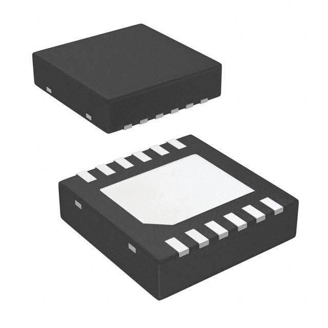
| 供应商器件封装 | 20-HTSSOP |
| 其它名称 | 296-35065-5 |
| 包装 | 管件 |
| 同步整流器 | 是 |
| 商标 | Texas Instruments |
| 安装类型 | 表面贴装 |
| 安装风格 | SMD/SMT |
| 封装 | Tube |
| 封装/外壳 | 20-TSSOP(0.173",4.40mm 宽)裸焊盘 |
| 封装/箱体 | HTSSOP-20 |
| 工作温度 | -40°C ~ 125°C |
| 工作温度范围 | - 40 C to + 125 C |
| 工厂包装数量 | 70 |
| 开关频率 | 1.6 MHz |
| 拓扑结构 | Buck |
| 最大工作温度 | + 125 C |
| 最大输入电压 | 17 V |
| 最小工作温度 | - 40 C |
| 最小输入电压 | 4.5 V |
| 标准包装 | 70 |
| 电压-输入 | 4.5 V ~ 17 V |
| 电压-输出 | 0.72 V ~ 15 V |
| 电流-输出 | 9A |
| 电源电压-最小 | 4.5 V |
| 类型 | Voltage Converter |
| 系列 | TPS56921 |
| 输入电压 | 4.5 V to 17 V |
| 输出数 | 1 |
| 输出电压 | 0.72 V to 1.48 V |
| 输出电流 | 9 A |
| 输出端数量 | 1 Output |
| 输出类型 | 可调式 |
| 频率-开关 | 200kHz ~ 1.6MHz |


- 商务部:美国ITC正式对集成电路等产品启动337调查
- 曝三星4nm工艺存在良率问题 高通将骁龙8 Gen1或转产台积电
- 太阳诱电将投资9.5亿元在常州建新厂生产MLCC 预计2023年完工
- 英特尔发布欧洲新工厂建设计划 深化IDM 2.0 战略
- 台积电先进制程称霸业界 有大客户加持明年业绩稳了
- 达到5530亿美元!SIA预计今年全球半导体销售额将创下新高
- 英特尔拟将自动驾驶子公司Mobileye上市 估值或超500亿美元
- 三星加码芯片和SET,合并消费电子和移动部门,撤换高东真等 CEO
- 三星电子宣布重大人事变动 还合并消费电子和移动部门
- 海关总署:前11个月进口集成电路产品价值2.52万亿元 增长14.8%


PDF Datasheet 数据手册内容提取
TPS56921 www.ti.com SLVSBL4–OCTOBER2012 4.5V to 17V Input, 9A Synchronous Step Down SWIFT™ Converter With VID Control CheckforSamples:TPS56921 FEATURES • OvercurrentProtectionforBothMOSFETs 1 • VIDControlRangeviaI2CCompatible withHiccupModeforSevereFaultConditions Interface: 0.72Vto1.48Vin10mVSteps • ThermalandOvervoltageProtection • I2CAddressingFlexibility:2BitsbyICpins • AdjustableSoftStart • ±1.5%OutputVoltageoverTemperaturefor • PowerGoodMonitorforUnder-andOver- VIDControl VoltageConditions • ±1%ReferenceVoltageoverTemperaturefor • OperatingJunctionTemperatureRange:–40°C ExternalRegulationMode to125°C • Integrated26mΩ /19mΩ MOSFETs • Availablein20-PinHTSSOPPackagewith PowerPADTM • PowerInputPVINVoltageRange:1.6Vto17V • SwitchingFrequency:200kHzto1.6MHz APPLICATIONS InternalOscillatororSynchronizingto ExternalClock • DigitalTVs • ShutdownCurrent:2µA • SetTopBoxes • MonotonicStart-UpintoPre-biasedOutput • SoCPower Voltage • HighDensityPowerDistributionSystems DESCRIPTION The TPS56921 in thermally enhanced 20-pin HTSSOP package is a full featured 17V, 9A synchronous step down converter which is optimized for small designs through high efficiency and integrating the high-side and low-side MOSFETs. After the initial power-up, the output voltage can be changed by codes sent to the IC via an I2CcompatibleVIDControlbus.Currentmodecontrolprovidesspacesavingsandeasycompensation. The output voltage startup ramp is controlled by the SS pin which helps to control startup inrush current. Power sequencing is supported by configuring the enable and the open drain power good pins. The output voltage is user-configurableatstartupbyexternalvoltagedivider. Cycle by cycle current limiting on the high-side fet protects the TPS56921 in overload situations and is enhanced by a low-side sourcing current limit which prevents current runaway. There is also a low-side sinking current limit which turns off the low-side MOSFET to prevent excessive reverse current. Hiccup protection will be triggered if the overcurrent condition has persisted for longer than the preset time. Thermal hiccup protection disables the part when die temperature exceeds thermal shutdown temperature and enables the part again after the built-in thermalhiccuptime. SIMPLIFIED SCHEMATIC EFFICIENCY Fsw = 500 kHz, V = 1.1 V OUT VIN PVIN PWRGD VIN 100 Cin Cboot 90 EN BOOT 80 VDD Rp2 Rp1 PH Lo VOUT % 70 VIN= 5V ADSSDDCRAL1 SASC1DLA VOUT Co R1 Efficiency- 34560000 VIN= 12V ADDR0 A0 VSENSE 20 SS RT/CLK R2 10 COMP GND 0 Css Rrt R3 PowerPAD 0 1 2 3 4 5 6 7 8 9 OutputCurrent-A C007 C1 1 Pleasebeawarethatanimportantnoticeconcerningavailability,standardwarranty,anduseincriticalapplicationsof TexasInstrumentssemiconductorproductsanddisclaimerstheretoappearsattheendofthisdatasheet. PRODUCTIONDATAinformationiscurrentasofpublicationdate. Copyright©2012,TexasInstrumentsIncorporated Products conform to specifications per the terms of the Texas Instruments standard warranty. Production processing does not necessarilyincludetestingofallparameters.
TPS56921 SLVSBL4–OCTOBER2012 www.ti.com Thesedeviceshavelimitedbuilt-inESDprotection.Theleadsshouldbeshortedtogetherorthedeviceplacedinconductivefoam duringstorageorhandlingtopreventelectrostaticdamagetotheMOSgates. ORDERINGINFORMATION(1) T PACKAGE PARTNUMBER J Tube TPS56921PWP –40°Cto125°C 20-PinHTSSOP LargeReel TPS56921PWPR (1) Forthemostcurrentpackageandorderinginformation,seethePackageOptionAddendumattheendofthisdocument,orseetheTI websiteatwww.ti.com. ABSOLUTE MAXIMUM RATINGS(1) overoperatingtemperaturerange(unlessotherwisenoted) VALUE UNIT VIN –0.3to20 PVIN –0.3to20 EN –0.3to6 BOOT –0.3to27 VSENSE –0.3to3 COMP –0.3to3 PWRGD –0.3to6 InputVoltage V SS –0.3to3 RT/CLK –0.3to6 VOUT –0.3to3.6 SDA –0.3to3.6 SCL –0.3to3.6 A0 –0.3to2.5 A1 –0.3to2.5 BOOT-PH 0to7.5 OutputVoltage PH –1to20 V PH10nsTransient –3to20 Vdiff(GNDtoexposedthermalpad) –0.2to0.2 V RT/CLK ±100 µA SourceCurrent PH CurrentLimit A PH CurrentLimit A PVIN CurrentLimit A SinkCurrent COMP ±200 µA PWRGD –0.1to5 mA ElectrostaticDischarge(HBM)QSS009-105(JESD22-A114A) 2 kV ElectrostaticDischarge(CDM)QSS009-147(JESD22-C101B.01) 500 V OperatingJunctionTemperature –40to125 °C StorageTemperature –65to150 °C (1) Stressesbeyondthoselistedunderabsolutemaximumratingsmaycausepermanentdamagetothedevice.Thesearestressratings only,andfunctionaloperationofthedeviceattheseoranyotherconditionsbeyondthoseindicatedunderrecommendedoperating conditionsisnotimplied.Exposuretoabsolute-maximum-ratedconditionsforextendedperiodsmayaffectdevicereliability. 2 SubmitDocumentationFeedback Copyright©2012,TexasInstrumentsIncorporated ProductFolderLinks:TPS56921
TPS56921 www.ti.com SLVSBL4–OCTOBER2012 THERMAL INFORMATION TPS56921 THERMALMETRIC(1)(2) UNITS HTSSOP(20PINS) θ Junction-to-ambientthermalresistance 39.4 JA θ Junction-to-ambientthermalresistance(3) 26 JA θ Junction-to-case(top)thermalresistance 26.5 JCtop θ Junction-to-boardthermalresistance 23.1 °C/W JB ψ Junction-to-topcharacterizationparameter 0.8 JT ψ Junction-to-boardcharacterizationparameter 22.8 JB θ Junction-to-case(bottom)thermalresistance 2.1 JCbot (1) Formoreinformationabouttraditionalandnewthermalmetrics,seetheICPackageThermalMetricsapplicationreport,SPRA953. (2) PowerratingataspecificambienttemperatureT shouldbedeterminedwithajunctiontemperatureof125°C.Thisisthepointwhere A distortionstartstosubstantiallyincrease.ThermalmanagementofthePCBshouldstrivetokeepthejunctiontemperatureatorbelow 125°Cforbestperformanceandlong-termreliability.Seepowerdissipationestimateinapplicationsectionofthisdatasheetformore information. (3) Testboardconditions: (a)3inches×3inches,4layers,thickness:0.062inch (b)2oz.coppertraceslocatedonthetopofthePCB (c)2oz.coppergroundplanesonthe2internallayersandbottomlayerofthePCB (d)21thermalviaslocatedunderthedevicepackageand9ofthemlocatedunderthedeviceexposedthermalpad ELECTRICAL CHARACTERISTICS T =–40°Cto125°C,VIN=4.5Vto17V,PVIN=1.6Vto17V(unlessotherwisenoted) J PARAMETER TESTCONDITIONS MIN TYP MAX UNIT SUPPLYVOLTAGE(VINANDPVINPINS) PVINoperatinginputvoltage 1.6 17 V VINoperatinginputvoltage 4.5 17 V VINinternalUVLOthreshold VINrising 4.0 4.5 V VINinternalUVLOhysteresis 150 mV VINshutdownsupplyCurrent EN=0V 2 7 μA VINoperating–nonswitchingsupplycurrent VSENSE=810mV 770 1000 μA ENABLEANDUVLO(ENPIN) Enablethreshold Rising 1.21 1.26 V Enablethreshold Falling 1.10 1.17 Inputcurrent EN=1.1V 1.15 μA Hysteresiscurrent EN=1.3V 3.3 μA OUTPUTVOLTAGE 0A≤I ≤9A OUT Voltagereference VoltageatVSENSEpinin 0.792 0. 0.808 V regulationbeforefirstI2Cwrite RelativetoidealVOUTafterfirst Ideal OutputVoltage I2Cwrite;(showninIdealVOUT IdealVOUT Ideal VOUT V –1.5% VOUT vs.Codetable) +1.5% MOSFET High-sideswitchresistance(1) BOOT-PH=3V 30 60 mΩ High-sideswitchresistance(1) BOOT-PH=6V 26 40 mΩ Low-sideSwitchResistance(1) 19 30 mΩ ERRORAMPLIFIER –2μA<I <2μA, ErroramplifierTransconductance(gm) COMP 1300 μMhos V =1V (COMP) Erroramplifierdcgain(productiontest) VSENSE=0.8V 1000 3000 V/V (1) Measuredatpins Copyright©2012,TexasInstrumentsIncorporated SubmitDocumentationFeedback 3 ProductFolderLinks:TPS56921
TPS56921 SLVSBL4–OCTOBER2012 www.ti.com ELECTRICAL CHARACTERISTICS (continued) T =–40°Cto125°C,VIN=4.5Vto17V,PVIN=1.6Vto17V(unlessotherwisenoted) J PARAMETER TESTCONDITIONS MIN TYP MAX UNIT V =1V,100mVinput Erroramplifiersource/sink (COMP) ±110 μA overdrive StartSwitchingThreshold 0.25 V COMPtoIswitchgm 24 A/V CURRENTLIMIT High-sideswitchcurrentlimitthreshold 11.5 17.5 22 A Low-sideswitchsourcingcurrentlimit 10 15.5 21 A Low-sideswitchsinkingcurrentlimit 2.5 4.5 6.5 A Hiccupwaittime 512 Cycles Hiccuptimebeforere-start 16384 Cycles THERMALSHUTDOWN Thermalshutdown 150 170 °C Thermalshutdownhysteresis 10 °C Thermalshutdownhiccuptime 32768 Cycles TIMINGRESISTORANDEXTERNALCLOCK(RT/CLKPIN) Maximumoperatingswitchingfrequency R(RT/CLK)=240kΩ(1%) 160 200 240 kHz Minimumoperatingswitchingfrequency R(RT/CLK)=100kΩ(1%) 400 480 560 kHz Switchingfrequency R(RT/CLK)=29kΩ(1% 1440 1600 1760 kHz Minimumpulsewidth 20 ns RT/CLKhighthreshold 2 V RT/CLKlowthreshold 0.78 V Measureat500kHzwithRT RT/CLKfallingedgetoPHrisingedgedelay 66 ns resistorinseries PLLfrequencyrange 200 1600 kHz PH(PHPIN) Measuredat90%to90%ofVIN, Minimumontime 94 150 ns 25°C,I =2A PH Minimumofftime BOOT-PH≥3V 0 % BOOT(BOOTPIN) BOOT-PHUVLO 2.1 3 V SLOWSTART(SSPIN) SSchargecurrent 2.3 μA POWERGOOD(PWRGDPIN) VSENSEthreshold VSENSEfalling(Fault) 92 %Vreg VSENSErising(Good) 94 %Vreg VSENSErising(Fault) 106 %Vreg VSENSEfalling(Good) 104 %Vreg VSENSE=Vref,V =5.5 Outputhighleakage (PWRGD) 30 100 nA V Outputlow I =2mA 0.3 V (PWRGD) MinimumVINforvalidoutput V <0.5Vat100μA 0.6 1 V (PWRGD) MinimumSSvoltageforPWRGD 1.4 V VOUT(VOUTPIN) OutputvoltageVIDcontrolminimum 0.72 V OutputvoltageVIDcontrolmaximum 1.48 V Outputvoltagestep 10 mV 4 SubmitDocumentationFeedback Copyright©2012,TexasInstrumentsIncorporated ProductFolderLinks:TPS56921
TPS56921 www.ti.com SLVSBL4–OCTOBER2012 ELECTRICAL CHARACTERISTICS (continued) T =–40°Cto125°C,VIN=4.5Vto17V,PVIN=1.6Vto17V(unlessotherwisenoted) J PARAMETER TESTCONDITIONS MIN TYP MAX UNIT SERIALINTERFACE(SDAANDSCLPINS)(2)(3) LOWlevelinputvoltage,V 0.9 V IL HIGHlevelinputvoltage,V 2.5 V IH Hysteresisofschmitttriggerinputs,V 0.16 V hys LOWlevelSDAoutputvoltage(Opendrain,3mA 0.4 V sinkcurrent),V OL1 Pulsewidthofspikessuppressedbyinputfilter, 50 ns t SP SCLclockfrequency,f 400 kHz scl Holdtime(repeated)STARTcondition,t 0.6 µs HD;STA LOWperiodofSCLclock,t 1.3 µs LOW HIGHperiodofSCLclock,t 0.6 µs HIGH Set-uptimeforarepeatedSTARTcondition, 0.6 µs t SU;STA Dataholdtime,t 50 900 ns HD;DAT Dataset-uptime,t 100 ns SU;DAT Risetime(SDAorSCL),t 20+0.1Cb(4) 300 ns r Falltime(SDAorSCL),t 20+0.1Cb(4) 300 ns f Set-uptimeforSTOPcondition,t 0.6 µs SU;STO BusfreetimebetweenSTOPandSTART 1.3 µs condition,t BUF Capacitiveloadforeachbusline,C 400 pF b (2) RefertotheI2CTimingdiagrambelowforI2CTimingDefinitions (3) Specifiedbydesign.Nottestedinproduction. (4) Cb=capacitanceofbuslineinpF I2CTimingDefinitions(ReproducedfromPhilipsI2CspecificationVersion1.1) Copyright©2012,TexasInstrumentsIncorporated SubmitDocumentationFeedback 5 ProductFolderLinks:TPS56921
TPS56921 SLVSBL4–OCTOBER2012 www.ti.com DEVICE INFORMATION PIN ASSIGNMENTS PWPPACKAGE (TOPVIEW) COMP 1 20 VOUT SS 2 19 VSENSE EN 3 18 VIN PH 4 17 PVIN Thermal PH 5 Pad 16 PVIN (21) PH 6 15 GND BOOT 7 14 GND PWRGD 8 13 RT/CLK A0 9 12 SCL A1 10 11 SDA PINFUNCTIONS PIN DESCRIPTION NAME NUMBER COMP 1 Erroramplifieroutput,andinputtotheoutputswitchcurrentcomparator.Connectfrequency compensationtothispin. SS 2 Anexternalcapacitorconnectedtothispinsetstheinternalvoltagereferencerisetime. EN 3 Enablepin.Floattoenable.Adjusttheinputundervoltagelockoutwithtworesistors. PH 4,5,6 Theswitchnode. BOOT 7 AbootstrapcapisrequiredbetweenBOOTandPH.Thevoltageonthiscapcarriesthegatedrive voltageforthehigh-sideMOSFET. PWRGD 8 PowerGoodfaultpin.Assertslowifoutputislowduetothermalshutdown,dropout,over-voltage,EN shutdownorduringslowstart. A0 9 LSBofchipaddress.TietoGNDfor0,leavefloatingfor1. A1 10 LSB+1ofchipaddress.TietoGNDfor0,leavefloatingfor1. SDA 11 DataI/Opin SCL 12 ClockI/Opin. RT/CLK 13 AutomaticallyselectsbetweenRTmodeandCLKmode.Anexternaltimingresistoradjuststheswitching frequencyofthedevice;InCLKmode,thedevicesynchronizestoanexternalclock. GND 14,15 ReturnforcontrolcircuitryandlowsidepowerMOSFET. PVIN 16,17 Powerinput.Suppliesthepowerswitchesofthepowerconverter. VIN 18 Suppliesthecontrolcircuitryofthepowerconverter. VSENSE 19 Invertingnodeofthegmerroramplifierinput. VOUT 20 OutputvoltagecontrolledbyVID Exposed 21 MustbeconnectedtoGNDandsoldereddownforproperelectricalandthermaloperation. ThermalPad 6 SubmitDocumentationFeedback Copyright©2012,TexasInstrumentsIncorporated ProductFolderLinks:TPS56921
TPS56921 www.ti.com SLVSBL4–OCTOBER2012 FUNCTIONALBLOCKDIAGRAM PWRGD EN VIN PVINPVIN Thermal Shutdown Shutdown UVLO Ip Ih CoEmnpaabrlaetor Shutdown Shutdown UV Logic Logic Enable Threshold OV Boot Charge MinimumClamp Current PulseSkip Sense INT ERROR VOUT AMPLIFIER Boot BOOT VSENSE EXT UVLO SS/TR HSMOSFET 0.8V INT Current VREF EXT Comparator PoDweeardS-Ttaimgee& ControlLogic PH PH VODUAT=C0.72 ComSpleonpseation PH to1.48V INT= VIDI2C 7bits OVoulttpaugte Selected VIN Regulator SSDCAK InSteerrfiaacle ROevceorlvoeardy MCaxlaimmupm OwsitchillPaLtoLr CLSurMreOntSLFimETit Current Sense A0 ChipAddr GND A1 01101A1A0 GND COMP RT/CLK POWERPAD EXT–ExternalRegulationMode INT-InternalRegulationMode Copyright©2012,TexasInstrumentsIncorporated SubmitDocumentationFeedback 7 ProductFolderLinks:TPS56921
TPS56921 SLVSBL4–OCTOBER2012 www.ti.com TYPICAL CHARACTERISTICS CHARACTERISTIC CURVES HIGH-SIDEMOSFETONRESISTANCEvsJUNCTION LOW-SIDEMOSFETONRESISTANCEvsJUNCTION TEMPERATURE TEMPERATURE 40 25 Ω VIN= 12 V Ω 22 VIN= 12 V m 35 m Resistance - 30 Resistance - 19 On On 16 - - rds(on) 25 rds(on) 13 20 10 –50 –25 0 25 50 75 100 125 –50 –25 0 25 50 75 100 125 TJ- JunctionTemperature - °C TJ- JunctionTemperature - °C Figure1. Figure2. VOLTAGEREFERENCEvsJUNCTIONTEMPERATURE OSCILLATORFREQUENCYvsJUNCTIONTEMPERATURE 0.804 485 RT= 100kΩ z Voltage Reference - V00..880020 cillator Frequency - kH448705 - Os VREF0.798 - SW470 F 0.796 465 –50 –25 0 25 50 75 100 125 –50 –25 0 25 50 75 100 125 T - JunctionTemperature - °C T - JunctionTemperature - °C J J Figure3. Figure4. SHUTDOWNQUIESCENTCURRENTvs ENPINHYSTERESISCURRENTvsJUNCTION INPUTVOLTAGE TEMPERATURE 4 3.8 A µ EN = 0V wn Quiescent Current - 32 TJ= 125°CTJ= 25°CTJ=–40°C sterisis Current - µA 33..76 VIN= 12 V do Hy ut 1 - 3.5 Sh Ih - Isd 0 3.4 3 6 9 12 15 18 –50 –25 0 25 50 75 100 125 VIN- Input Voltage - V TJ- JunctionTemperature - °C Figure5. Figure6. 8 SubmitDocumentationFeedback Copyright©2012,TexasInstrumentsIncorporated ProductFolderLinks:TPS56921
TPS56921 www.ti.com SLVSBL4–OCTOBER2012 TYPICAL CHARACTERISTICS (continued) ENPINPULLUPCURRENTvsJUNCTIONTEMPERATURE ENPINUVLOTHRESHOLDvsJUNCTIONTEMPERATURE 1.9 1.24 V = 12 V IN 1.8 nt - µA 1.7 hold - V1.23 Curre 1.6 Thres1.22 p O Pullu 1.5 UVL I- p EN - 1.21 1.4 1.3 1.20 –50 –25 0 25 50 75 100 125 –50 –25 0 25 50 75 100 125 T - JunctionTemperature - °C T - JunctionTemperature - °C J J Figure7. Figure8. V NON-SWITCHINGOPERATINGQUIESCENTCURRENT IN vs SLOWSTARTCHARGECURRENTvs INPUTVOLTAGE JUNCTIONTEMPERATURE 900 2.5 nt ese TJ= 125°C A g Qui 800 TJ= 25°C nt - µ 2.4 n e hing OperatiCurrent - µA700 TJ=–40°C Charge Curr 2.3 witc SS Nons 600 I- SS2.2 - q I 500 2.1 3 6 9 12 15 18 –50 –25 0 25 50 75 100 125 VIN- Input Voltage - V TJ- JunctionTemperature - °C Figure9. Figure10. HIGH-SIDECURRENTLIMITTHRESHOLDvsINPUT PWRGDTHRESHOLDvsJUNCTIONTEMPERATURE VOLTAGE 110 20 V = 12 V VSENSE Rising IN 19 A nt - µA VSENSE Falling hold - 18 TJ=–40°C Curre Thres 17 T = 25°C ge 100 mit J Char nt Li 16 - SS VSENSE Rising Curre 15 TJ= 125°C ISS I- cl 14 VSENSE Falling 90 13 –50 –25 0 25 50 75 100 125 3 6 9 12 15 18 TJ- JunctionTemperature - °C VIN- Input Voltage - V Figure11. Figure12. Copyright©2012,TexasInstrumentsIncorporated SubmitDocumentationFeedback 9 ProductFolderLinks:TPS56921
TPS56921 SLVSBL4–OCTOBER2012 www.ti.com TYPICAL CHARACTERISTICS (continued) MINIMUMCONTROLLABLEONTIMEvsJUNCTION MINIMUMCONTROLLABLEDUTYRATIOvsJUNCTION TEMPERATURE TEMPERATURE s130 % 7.0 me - n VIN= 12 V atio - RVT== 1 1020 kVΩ Ti120 R IN On uty 6.0 able 110 ble D ontroll ntrolla 5.0 C o um 100 m C m u - Minin 90 - Minim 4.0 nmi min To 80 D 3.0 –50 –25 0 25 50 75 100 125 –50 –25 0 25 50 75 100 125 TJ- JunctionTemperature - °C TJ- JunctionTemperature - °C Figure13. Figure14. BOOT-PHUVLOTHRESHOLDvsJUNCTIONTEMPERATURE 2.2 A µ d - ol h s e hr T O L V 2.1 U H P T- O O B - ot o b V 2.0 –50 –25 0 25 50 75 100 125 T - JunctionTemperature - °C J Figure15. 10 SubmitDocumentationFeedback Copyright©2012,TexasInstrumentsIncorporated ProductFolderLinks:TPS56921
TPS56921 www.ti.com SLVSBL4–OCTOBER2012 OVERVIEW The TPS56921 is a 17-V, 9-A, synchronous step-down (buck) converter with two integrated n-channel MOSFETs.ToimproveperformanceduringlineandloadtransientstheTPS56921implementsafixedfrequency, peak current mode control which also simplifies external frequency compensation. The output voltage of the TPS56921 can be set by either VSENSE with divider resistors (Adjusting the Output Voltage by External Regulation Mode) or I2C compatible interface (Programming the Output Voltage by Internal Regulation Mode) to aslowasthe0.8Vreferencevoltageinexternalregulationmodeor0.72Vininternalregulationmode.Itoperates in CCM (Continuous current mode) at any load conditions unless the COMP pin voltage drops below the COMP pinstartswitchingthreshold(typically0.25V). The wide switching frequency of 200 kHz to 1600 kHz allows for efficiency and size optimization when selecting the output filter components. The RT/CLK pin is dual-functional with two modes. In RT mode, the switching frequency is adjusted using a resistor to ground on the RT/CLK pin. In CLK mode, the TPS56921 can be controlledbytheRT/CLKpintosynchronizetheswitchingcycletothefallingedgeofanexternalsystemclock. The TPS56921 has been designed for safe startup into pre-biased outputs. The default start up is when VIN is typically 4.0V. The EN pin has an internal pull-up current source that can be used to adjust the input voltage under-voltage lockout (UVLO) with two external resistors. In addition, the EN pin can be floating for the TPS56921 to operate with the internal pull up current. The total operating current for the TPS56921 is approximately 770μA when not switching and under no load. When the TPS56921 is disabled, the supply current istypicallylessthan2μA. The integrated MOSFETs allow for high efficiency power supply designs with continuous output currents up to 9 amperes.TheMOSFETshavebeensizedtooptimizeefficiencyforlowerdutycycleapplications. The TPS56921 reduces the external component count by integrating the boot recharge circuit. The bias voltage for the integrated high-side MOSFET is supplied by a capacitor between the BOOT and PH pins. The bootstrap voltage is monitored by a BOOT to PH UVLO (BOOT-PH UVLO) circuit allowing PH pin to be pulled low to recharge the boot capacitor. The TPS56921 can operate at 100% duty cycle as long as the boot capacitor voltageishigherthanthepresetBOOT-PHUVLOthresholdwhichistypically2.1V. The TPS56921 has a power good comparator (PWRGD) with hysteresis which monitors the output voltage through the VSENSE pin. The PWRGD pin is an open drain MOSFET which is pulled low when the VSENSE pin voltage is less than 92% or greater than 106% of the internal reference voltage and asserts high when it is 94% to104%oftheinternalreferencevoltage. The slow start (SS) pin is used to minimize inrush currents or provide power supply sequencing during power up. A small value capacitor or resistor divider should be coupled to the pin for slow start or critical power supply sequencingrequirements. The TPS56921 is protected from output overvoltage, overcurrent and overheat conditions. The TPS56921 minimizes excessive output overvoltage transients by taking advantage of the overvoltage circuit power good comparator. When the overvoltage comparator is activated, the high-side MOSFET is turned off and prevented from turning on until the VSENSE pin voltage is lower than 104% of the Vref. The TPS56921 implements both high-side MOSFET overload protection and bidirectional low-side MOSFET overload protections which help control the inductor current and avoid current runaway. If the overcurrent condition has lasted for more than the hiccupwaittime,theTPS56921willshutdownandre-startafterthehiccuptime.TheTPS56921alsoshutsdown if the junction temperature is higher than thermal shutdown trip point. When the junction temperature drops 10°C typically below the thermal shutdown trip point, the built-in thermal shutdown hiccup timer is triggered. The TPS56921 will be restarted under control of the slow start circuit automatically after the thermal shutdown hiccup timeisover. Furthermore, if the overcurrent condition has lasted for more than the hiccup wait time which is programmed for 512 switching cycles, the TPS56921 will shut down itself and re-start after the hiccup time which is set for 16384 cycles.Thehiccupmodehelpstoreducethedevicepowerdissipationundersevereovercurrentconditions. Copyright©2012,TexasInstrumentsIncorporated SubmitDocumentationFeedback 11 ProductFolderLinks:TPS56921
TPS56921 SLVSBL4–OCTOBER2012 www.ti.com DETAILED DESCRIPTION Fixed Frequency PWM Control The device uses a adjustable fixed frequency, peak current mode control. The output voltage is compared through external resistors on the VSENSE pin to an internal voltage reference by an error amplifier which drives the COMP pin. An internal oscillator initiates the turn on of the high-side power switch. The error amplifier output is converted into a current reference which compares to the high-side power switch current. When the power switch current reaches current reference generated by the COMP voltage level the high-side power switch is turnedoffandthelow-sidepowerswitchisturnedon. Continuous Current Mode Operation (CCM) As a synchronous buck converter, the device normally works in CCM (Continuous Conduction Mode) under load allconditions. VIN and Power VIN Pins (VIN and PVIN) The device allows for a variety of applications by using the VIN and PVIN pins together or separately. The VIN pin voltage supplies the internal control circuits of the device. The PVIN pin voltage provides the input voltage to thepowerconvertersystem. If tied together, the input voltage for VIN and PVIN can range from 4.5V to 17V. If using the VIN separately from PVIN, the VIN pin must be between 4.5V and 17V, and the PVIN pin can range from as low as 1.6V to 17V. A voltage divider connected to the EN pin can adjust the either input voltage UVLO appropriately. Adjusting the inputvoltageUVLOonthePVINpinhelpstoprovideconsistentpowerupbehavior. Setting the Output Voltage TheoutputvoltagecanbesetviaAdjustingtheOutputVoltagebyExternalRegulationModeorProgrammingthe OutputVoltagebyInternalRegulationMode.Intheexternalregulationmode,theoutputvoltageisdeterminedby the output voltage resistor divider and it can never be lower than the internal voltage reference of 0.8 V. In the internal regulation mode, the output voltage is controlled by I2C compatible interface via SDA, SCL, A0 and A1 pinsbetween0.72Vand1.48V. The device always starts up into external regulation mode. The first I2C write will not be taken until the VSENSE pin achieves regulation at the conclusion of soft start. Use Equation 1 to calculation the nominal time between the device start and the conclusion of soft start where Css is the slow start capacitor and the slow start charge current(Iss)is2.3μA. C (nF) ´1.2 (V) t (ms) = SS WAIT I (mA) SS (1) The device stays in external regulation mode until the first successful I2C write excluding the special control codeslistedinTable4,thenthedeviceswitchestointernalregulationmode. If the serial interface is to be used, the VOUT pin should be connected to the output of the converter and the outputvoltageatVOUTpinoverridestheoutputvoltageresistordividersetting.Inthisconfiguration,theoutputof theconvertercannotgoabove3.3V. If the serial interface will not be used, the VOUT pin should be floating and the output of the converter can be set greaterthan3.3Vbytheoutputvoltageresistordivider. Adjusting the Output Voltage by External Regulation Mode Theoutputvoltageissetwitharesistordividerfromtheoutput(VOUT)totheVSENSEpin.Itisrecommendedto use 1% tolerance or better divider resistors. Referring to the application schematic of Figure 25, start with a 10 kΩforR10anduseEquation25tocalculateR11.Toimproveefficiencyatlightloadsconsiderusinglargervalue resistors. If the values are too high the regulator is more susceptible to noise and voltage errors from the VSENSEinputcurrentarenoticeable. 12 SubmitDocumentationFeedback Copyright©2012,TexasInstrumentsIncorporated ProductFolderLinks:TPS56921
TPS56921 www.ti.com SLVSBL4–OCTOBER2012 The minimum output voltage and maximum output voltage can be limited by the minimum on time of the high- side MOSFET and bootstrap voltage (BOOT-PH voltage) respectively. More discussions are located in Minimum On Time and Maximum Switching Frequency Limitations and Bootstrap Voltage (BOOT) and Low Dropout Operation. Minimum On Time and Maximum Switching Frequency Limitations The current-mode architecture of the device requires a settling time before accurate current measurements can occur, therefore a minimum on-time spec exists. The output voltage may be limited by the minimum controllable on time depending on the input voltage, load current and switching frequency, and so on. The minimum output voltageisgivenbyEquation2. Voutmin = Ontimemin•Fsmax(Vinmax + Ioutmin(Rds,ls - Rds,hs))- Ioutmin(RL + Rds,ls) (2) Where: Voutmin=minimumachievableoutputvoltage Ontimemin=minimumcontrollableon-time(150nsecmaximum@2Aloadcurrent) Fsmax=maximumswitchingfrequencyincludingtolerance Vinmax=maximuminputvoltage Ioutmin=minimumloadcurrent Rds,hs=highsideMOSFETonresistance(26mΩ typical) Rds,ls=lowsideMOSFETonresistance(19mΩtypical) RL=seriesresistanceofoutputinductor If the minimum on-time limitation is exceeded, the device may begin pulse-skipping. In this case, the device will act as if the operational switching frequency has dropped, but in reality it may probably only skip a few cycles. Thoughthiswillincreasetheoutputripple,theoutputoftheconverterwillremaininregulation.Itisuptotheuser to determine whether to choose a switching frequency that keeps the operation away from the pulse-skipping regime of operation or to run at a reduced input voltage to keep the operation away from pulse-skipping mode or torunahigherfrequencythatmaypulse-skipifthedutyratiobecomestoolow. Safe Start-up into Pre-Biased Outputs The device has been designed to prevent the low-side MOSFET from discharging a pre-biased output. During monotonic pre-biased startup, the low-side MOSFET is not allowed to sink current until the SS pin voltage is higherthan1.4V. Error Amplifier Thedeviceusesatransconductanceerroramplifier.TheerroramplifiercomparestheVSENSEpinvoltagetothe lower of the SS pin voltage or the internal 0.8V voltage reference. The transconductance of the error amplifier is 1300 μA/V during normal operation. The frequency compensation network is connected between the COMP pin andground. Slope Compensation The device adds a compensating ramp to the switch current signal. This slope compensation prevents sub- harmonicoscillations.Theavailablepeakinductorcurrentremainsconstantoverthefulldutycyclerange. Enable and Adjusting Under-Voltage Lockout (EN and UVLO) The EN pin provides electrical on/off control of the device. Once the EN pin voltage exceeds the threshold voltage, the device starts operation. If the EN pin voltage is pulled below the threshold voltage, the regulator stopsswitchingandenterslowIqstate. Copyright©2012,TexasInstrumentsIncorporated SubmitDocumentationFeedback 13 ProductFolderLinks:TPS56921
TPS56921 SLVSBL4–OCTOBER2012 www.ti.com The EN pin has an internal pull-up current source, allowing the user to float the EN pin for enabling the device. If an application requires controlling the EN pin, use open drain or open collector output logic to interface with the pin. The device implements internal UVLO circuitry on the VIN pin. The device is disabled when the VIN pin voltage fallsbelowtheinternalVINUVLOthreshold.TheinternalVINUVLOthresholdhasahysteresisof150mV. If an application requires either a higher UVLO threshold on the VIN pin or a secondary UVLO on the PVIN, in split rail applications, then the EN pin can be configured as shown in Figure 16, Figure 17 and Figure 18. When usingtheexternalUVLOfunctionitisrecommendedtosetthehysteresistobegreaterthan500mV. The EN pin has a small pull-up current Ip which sets the default state of the pin to enable when no external components are connected. The pull-up current is also used to control the voltage hysteresis for the UVLO function since it increases by I once the EN pin crosses the enable threshold. The UVLO thresholds can be h calculatedusingEquation3andEquation4. TPS56921 VIN ip ih R1 R2 EN Figure16. AdjustableVINUnderVoltageLockOut TPS56921 PVIN ip ih R1 R2 EN Figure17. AdjustablePVINUnderVoltageLockOut,VIN≥ 4.5V TPS56921 PVIN VIN ip ih R1 R2 EN Figure18. AdjustableVINandPVINUnderVoltageLockOut 14 SubmitDocumentationFeedback Copyright©2012,TexasInstrumentsIncorporated ProductFolderLinks:TPS56921
TPS56921 www.ti.com SLVSBL4–OCTOBER2012 æV ö V ç ENFALLING ÷ - V START STOP è VENRISING ø R1= æ V ö I ç1- ENFALLING ÷+I p h è VENRISING ø (3) R1´V R2 = ENFALLING V -V +R1(I +I ) STOP ENFALLING p h (4) WhereI =3.3μA,I =1.15μA,V =1.21V,V =1.17V h p ENRISING ENFALLING Setting Switching Frequency and Synchronization (RT/CLK) TheRT/CLKpincanbeusedtosettheswitchingfrequencyofthedeviceintwomodes. In RT mode, a resistor (RT resistor) is connected between the RT/CLK pin and GND. The switching frequency of the device is adjustable from 200 kHz to 1600 kHz by placing a maximum of 240 kΩ and minimum of 29 kΩ respectively.InCLKmode,anexternalclockisconnecteddirectlytotheRT/CLKpin.Thedeviceissynchronized totheexternalclockfrequencywithPLL. The CLK mode overrides the RT mode. The device is able to detect the proper mode automatically and switch fromtheRTmodetoCLKmode. Adjustable Switching Frequency (RT Mode) To determine the RT resistance for a given switching frequency, use Equation 5 or the curve in Figure 19. To reduce the solution size one would set the switching frequency as high as possible, but tradeoffs of the supply efficiencyandminimumcontrollableontimeshouldbeconsidered. Rrt(kW) = 48000×Fsw(kHz)-0.997 -2 (5) 250 200 Wk − ce 150 n a st si Re 100 − T R 50 0 200 400 600 800 1000 1200 1400 1600 Fsw − Oscillator Frequency − kHz Figure19. RTSetResistorvsSwitchingFrequency Synchronization (CLK mode) An internal Phase Locked Loop (PLL) has been implemented to allow synchronization between 200kHz and 1600kHz,andtoeasilyswitchfromRTmodetoCLKmode. To implement the synchronization feature, connect a square wave clock signal to the RT/CLK pin with a duty cycle between 20% to 80%. The clock signal amplitude must transition lower than 0.78V and higher than 2.0V. ThestartoftheswitchingcycleissynchronizedtothefallingedgeofRT/CLKpin. Copyright©2012,TexasInstrumentsIncorporated SubmitDocumentationFeedback 15 ProductFolderLinks:TPS56921
TPS56921 SLVSBL4–OCTOBER2012 www.ti.com In applications where both RT mode and CLK mode are needed, the device can be configured as shown in Figure 20. Before the external clock is present, the device works in RT mode and the switching frequency is set by RT resistor. When the external clock is present, the CLK mode overrides the RT mode. The first time the SYNC pin is pulled above the RT/CLK high threshold (2.0V), the device switches from the RT mode to the CLK mode and the RT/CLK pin becomes high impedance as the PLL starts to lock onto the frequency of the external clock. It is not recommended to switch from the CLK mode back to the RT mode because the internal switching frequencydropsto100kHzfirstbeforereturningtotheswitchingfrequencysetbyRTresistor. RT/CLK TPS54622 mode select TPS56921 RT/CLK Rrt Figure20. WorkswithBothRTmodeandCLKmode Slow Start (SS) The device uses the lower voltage of the internal voltage reference or the SS pin voltage as the reference voltage and regulates the output accordingly. A capacitor on the SS pin to ground implements a slow start time. The device has an internal pull-up current source of 2.3μA that charges the external slow start capacitor. The calculations for the slow start time (Tss, 10% to 90%) and slow start capacitor (Css) are shown in Equation 6. Thevoltagereference(Vref)is0.8Vandtheslowstartchargecurrent(Iss)is2.3μA. Css(nF) ´ Vref(V) Tss(ms)= Iss(mA) (6) When the input UVLO is triggered, the EN pin is pulled below 1.21V, or a thermal shutdown event occurs the device stops switching and enters low current operation. At the subsequent power up, when the shutdown condition is removed, the device does not start switching until it has discharged its SS pin to ground ensuring propersoftstartbehavior. Power Good (PWRGD) The PWRGD pin is an open drain output. Once the VSENSE pin is between 94% and 104% of the internal voltage reference the PWRGD pin pull-down is de-asserted and the pin floats. It is recommended to use a pull- up resistor between the values of 10kΩ and 100kΩ to a voltage source that is 5.5V or less. The PWRGD is in a defined state once the VIN input voltage is greater than 1V but with reduced current sinking capability. The PWRGDachievesfullcurrentsinkingcapabilityoncetheVINinputvoltageisabove4.5V. The PWRGD pin is pulled low when VSENSE is lower than 92% or greater than 106% of the nominal internal reference voltage. Also, the PWRGD is pulled low, if the input UVLO or thermal shutdown are asserted, the EN pinispulledlowortheSSpinisbelow1.4V. In internal regulation mode, to avoid PWRGD jitters due to large jumps in the I2C-controlled Vout setting, it is possible to “blank” the PWRGD being pulled down for some number of CLK cycles. Please refer to Explanation ofSpecialCodes-PWRGDBlankingControlCodesforthedetails. Bootstrap Voltage (BOOT) and Low Dropout Operation The device has an integrated boot regulator, and requires a small ceramic capacitor between the BOOT and PH pins to provide the gate drive voltage for the high-side MOSFET. The boot capacitor is charged when the BOOT pin voltage is less than VIN and BOOT-PH voltage is below regulation. The value of this ceramic capacitor should be 0.1μF. A ceramic capacitor with an X7R or X5R grade dielectric with a voltage rating of 10V or higher isrecommendedbecauseofthestablecharacteristicsovertemperatureandvoltage. 16 SubmitDocumentationFeedback Copyright©2012,TexasInstrumentsIncorporated ProductFolderLinks:TPS56921
TPS56921 www.ti.com SLVSBL4–OCTOBER2012 To improve drop out, the device is designed to operate at 100% duty cycle as long as the BOOT to PH pin voltage is greater than the BOOT-PH UVLO threshold which is typically 2.1V. When the voltage between BOOT and PH drops below the BOOT-PH UVLO threshold the high-side MOSFET is turned off and the low-side MOSFET is turned on allowing the boot capacitor to be recharged. In applications with split input voltage rails 100%dutycycleoperationcanbeachievedaslongas(VIN–PVIN) >4V. Output Overvoltage Protection (OVP) The device incorporates an output overvoltage protection (OVP) circuit to minimize output voltage overshoot. For example, when the power supply output is overloaded the error amplifier compares the actual output voltage to the internal reference voltage. If the VSENSE pin voltage is lower than the internal reference voltage for a considerable time, the output of the error amplifier demands maximum output current. Once the condition is removed, the regulator output rises and the error amplifier output transitions to the steady state voltage. In some applications with small output capacitance, the power supply output voltage can respond faster than the error amplifier. This leads to the possibility of an output overshoot. The OVP feature minimizes the overshoot by comparing the VSENSE pin voltage to the OVP threshold. If the VSENSE pin voltage is greater than the OVP thresholdthehigh-sideMOSFETisturnedoffpreventingcurrentfromflowingtotheoutputandminimizingoutput overshoot. When the VSENSE voltage drops lower than the OVP threshold, the high-side MOSFET is allowed to turnonatthenextclockcycle. Overcurrent Protection The device is protected from overcurrent conditions by cycle-by-cycle current limiting on both the high-side MOSFETandthelow-sideMOSFET. High-sideMOSFETovercurrentprotection The device implements current mode control which uses the COMP pin voltage to control the turn off of the high- side MOSFET and the turn on of the low-side MOSFET on a cycle by cycle basis. Each cycle the switch current and the current reference generated by the COMP pin voltage are compared, when the peak switch current intersectsthecurrentreferencethehigh-sideswitchisturnedoff. Low-sideMOSFETovercurrentprotection While the low-side MOSFET is turned on its conduction current is monitored by the internal circuitry. During normal operation the low-side MOSFET sources current to the load. At the end of every clock cycle, the low-side MOSFET sourcing current is compared to the internally set low-side sourcing current limit. If the low-side sourcing current is exceeded the high-side MOSFET is not turned on and the low-side MOSFET stays on for the next cycle. The high-side MOSFET is turned on again when the low-side current is below the low-side sourcing currentlimitatthestartofacycle. The low-side MOSFET may also sink current from the load. If the low-side sinking current limit is exceeded the low-side MOSFET is turned off immediately for the rest of that clock cycle. In this scenario both MOSFETs are offuntilthestartofthenextcycle. Furthermore, if an output overload condition (as measured by the COMP pin voltage) has lasted for more than the hiccup wait time which is programmed for 512 switching cycles, the device will shut down itself and restart after the hiccup time of 16384 cycles. The hiccup mode helps to reduce the device power dissipation under severeovercurrentconditions. Overheat Protection The internal thermal shutdown circuitry forces the device to stop switching if the junction temperature exceeds 170°C typically. Once the junction temperature drops below 160°C typically, the internal thermal hiccup timer will start to count. The device reinitiates the power up sequence after the built-in thermal shutdown hiccup time (32768cycles)isover. Copyright©2012,TexasInstrumentsIncorporated SubmitDocumentationFeedback 17 ProductFolderLinks:TPS56921
TPS56921 SLVSBL4–OCTOBER2012 www.ti.com Programming the Output Voltage by Internal Regulation Mode On the TPS56921, the serial bus is inactive until the chip is enabled and the soft start time has elapsed. Until then, the serial bus will ignore communications and will not acknowledge. During this time, the TPS56921’s output voltage will be determined by the external resistor divider feedback to the VSENSE pin. When SS crosses 1.2V the serial interface becomes active and the user may program VOUT by writing to the interface via SDA and SCL. On the first successful I2C write, the device switches to internal regulation mode. In internal regulation mode,theVOUTpinservesasthefeedbackpath,andtheVSENSEpinvoltageisignored. I2C Compatible Interface The TPS56921 implements a subset of the Philips I2C specification Ver. 1.1. The TPS56921 is a slave-only (it does not write data to the I2C bus), and a complete I2C transaction consists of writing the TPS56921’s 8-bit address / direction byte followed by a single 8-bit data byte. Long-form address modes and multi-byte data transfers are not supported in this implementation. If the TPS56921 fails to acknowledge either of these two bytes,themastershouldconsiderthetransfertobeafailure,andshouldissueaSTOPcommandandtryagain. The serial interface pins are composed of the SDA (Data) and SCL (Clock) pins, and the A0 and A1 pins to set up the chip’s address. SDA and SCL are designed to be used with pullup resistors to 3.3V. A0 and A1 are designedtobeeithergrounded(logicLOW)orleftopen(logicHIGH)andshouldnottietoahighvoltage. I2C Compatible Protocol Inputvoltage Logic levels for the serial interface are not fixed. For the TPS56921, a logic “0” (LOW) should be 0V and a logic “1” (HIGH)canbeanyvoltagebetween2.5Vand3.3V.LogicHIGHisgeneratedbyexternalpullupresistors(see nextparagraph). Outputvoltage Theserialbushasexternalpullupresistors,oneforSCLandoneforSDA.ThesepulluptoavoltagecalledVDD which must lie between 2.5V and 3.3V. The outputs are pulled down to their logic LOW levels by open-drain outputs and pulled up to their logic HIGH levels by these external pullups. The pullups must be selected so that thecurrentintoanychipwhenpulledLOWbythatchip’sopendrainoutput(=VDD/RPULLUP)islessthan3mA. Dataformat One clock pulse on the SCL clock line is generated for each bit of data to be transferred. The data on the SDA line must be stable during the HIGH period of the SCK clock line. The HIGH or LOW state of the data line can only change when the clock signal on the SCL line is LOW. The MSB of the address and data bytes are sent first,thatisD[6]oftheaddressbyteandtheChkSumbitforthedatabyte. StartandStopconditions A HIGH to LOW transition on the SDA line while the SCL line is HIGH defines a START condition. A LOW to HIGH transition on the SDA line while the SCL line is HIGH defines a STOP condition. START and STOP conditions are always generated by the Master. The bus is considered to be BUSY after the condition. It is consideredtobefreeagainafteraminimumof1.3µSaftertheSTOPcondition. The bus stays busy if a repeated START (Sr) is generated instead of a STOP condition. START and repeated STARTarefunctionallyidentical. Every byte of data out on the SDA line is 8 bits long. 9 clocks occur for each byte (the additional clock being for an ACK signal put onto the bus by the TPS56921 pulling down on the bus to acknowledge receipt of the data). Exactly two bytes should be transferred to the TPS56921 per transfer, a 7-bit address and R/W byte followed by adatabyteasshowninthefollowingwaveform: 18 SubmitDocumentationFeedback Copyright©2012,TexasInstrumentsIncorporated ProductFolderLinks:TPS56921
TPS56921 www.ti.com SLVSBL4–OCTOBER2012 Always 0 for TPS56921 ACompleteAddressandDataTransfer-AdaptedfromPhilipsI2CSpecification When the TPS56921 receives an address code it recognizes to be its own, it will respond by sending an ACK (pulling down on the SDA bus during clock 9 on the SCL bus). If the address is not recognized, the TPS56921 assumes that the I2C message is intended for another chip on the bus, and it takes no action. It will disregard datasentthereafteruntilthenextSTARTisbegun. If, after recognizing its address, the TPS56921 receives a valid data byte (checked by comparing the ChkSum sent to the D[6:0] data), it will send an ACK and will set the output voltage to the desired value. If the byte is deemed invalid, ACK will not be sent and the Master will need to retry by sending a new START sequence and aninitiatingresendoftheentireaddress/datapacket. I2C Address Byte The 7-bit address of the TPS56921 can be any number between 34h (0110100) and 37h (0110111). The 5 MSBs are set internally and the 2 LSBs are customer-selectable via the A1 and A0 pins, allowing up to 4 TPS56921s to be controlled on the same serial bus. When the Master is sending the address as an 8-bit value, the 7-bit address should be sent followed by a trailing 0 to indicate this is a WRITE operation. The following codesassumethistrailingzero. Table1.TPS56921AddressasaFunctionofA1andA0Pins A1 A0 TPS56921Address(binary) TPS56921Address(hex) Ground(0) Ground(0) 01101000 68h Ground(0) Open(1) 01101010 6Ah Open(1) Ground(0) 01101100 6Ch Open(1) Open(1) 01101110 6Eh I2C Data Byte The 8 bits of data sent over the serial bus controls the VOUT of the TPS56921. After the SoftStart time has elapsed (SS pin voltage goes above approx. 1.23V), the serial interface becomes active and the user may programVOUTbywritingtotheinterface.Thedataisstructuredthus: Table2.StructureofTPS56921Databyte 8 7 6 5 4 3 2 1 ChkSum D6 D5 D4 D3 D2 D1 D0 D[6:0] – These bits are the 7-bit selector for one of 77 output voltages. The voltages are selected from the followingtable: Table3.IdealVOUTvs.Code Code Binary VOUT Code Binary VOUT Code Binary VOUT 0 0000000 0.720 26 0011010 0.980 52 0110100 1.240 Copyright©2012,TexasInstrumentsIncorporated SubmitDocumentationFeedback 19 ProductFolderLinks:TPS56921
TPS56921 SLVSBL4–OCTOBER2012 www.ti.com Table3.IdealVOUTvs.Code(continued) Code Binary VOUT Code Binary VOUT Code Binary VOUT 0 0000000 0.720 26 0011010 0.980 52 0110100 1.240 1 0000001 0.730 27 0011011 0.990 53 0110101 1.250 2 0000010 0.740 28 0011100 1.000 54 0110110 1.260 3 0000011 0.750 29 0011101 1.010 55 0110111 1.270 4 0000100 0.760 30 0011110 1.020 56 0111000 1.280 5 0000101 0.770 31 0011111 1.030 57 0111001 1.290 6 0000110 0.780 32 0100000 1.040 58 0111010 1.300 7 0000111 0.790 33 0100001 1.050 59 0111011 1.310 8 0001000 0.800 34 0100010 1.060 60 0111100 1.320 9 0001001 0.810 35 0100011 1.070 61 0111101 1.330 10 0001010 0.820 36 0100100 1.080 62 0111110 1.340 11 0001011 0.830 37 0100101 1.090 63 0111111 1.350 12 0001100 0.840 38 0100110 1.100 64 1000000 1.360 13 0001101 0.850 39 0100111 1.110 65 1000001 1.370 14 0001110 0.860 40 0101000 1.120 66 1000010 1.380 15 0001111 0.870 41 0101001 1.130 67 1000011 1.390 16 0010000 0.880 42 0101010 1.140 68 1000100 1.400 17 0010001 0.890 43 0101011 1.150 69 1000101 1.410 18 0010010 0.900 44 0101100 1.160 70 1000110 1.420 19 0010011 0.910 45 0101101 1.170 71 1000111 1.430 20 0010100 0.920 46 0101110 1.180 72 1001000 1.440 21 0010101 0.930 47 0101111 1.190 73 1001001 1.450 22 0010110 0.940 48 0110000 1.200 74 1001010 1.460 23 0010111 0.950 49 0110001 1.210 75 1001011 1.470 24 0011000 0.960 50 0110010 1.220 76 1001100 1.480 25 0011001 0.970 51 0110011 1.230 >76 >1001100 Illegal/ Special 20 SubmitDocumentationFeedback Copyright©2012,TexasInstrumentsIncorporated ProductFolderLinks:TPS56921
TPS56921 www.ti.com SLVSBL4–OCTOBER2012 Anycode>76isillegalexceptforthefollowingspecialcontrolcodes: Table4.SpecialControlCodes SpecialCode Function 1111000 SetdelayfromPWRGDfaulttoPWRGDpinpulldowntozero 1111001 SetdelayfromPWRGDfaulttoPWRGDpinpulldownto4CLKcycles(default) 1111010 SetdelayfromPWRGDfaulttoPWRGDpinpulldownto8CLKcycles 1111011 SetdelayfromPWRGDfaulttoPWRGDpinpulldownto4CLKcycles(default) 1111111 Changebacktoexternalregulationmode Explanation of Special Codes - PWRGD Blanking Control Codes Especially for low load currents, large jumps in the I2C-controlled Vout setting may have a long settling time comparedtotheUV/OVthresholds.Ifthishappens,itwillcausethePWRGDsignaltotemporarilyindicateafault condition. If this is not the desired behavior, it is possible to “blank” the PWRGD being pulled down for some number of CLK cycles, whether the CLK frequency is being set by an RT resistor or by an external CLK at the RT/CLK pin. The user can set this delay to 4, 8 or 16 CLK cycles using the 11110xx codes shown on the previous page. On power-up, the delay defaults to 4 clock cycles. The user can reset the blanking time using these codes at any timewithoutaffectinganyotherdevicebehavior. Alternatively, the user can avoid this by sequentially programming the VOUT in smaller steps. This method allows the system enough time to respond to large VOUT transitions. The same behavior can occur when changing from external to internal mode, so the user should first select a VOUT equal to the externally-set VOUT,thenmoveinsmallstepstothedesiredVOUT. Explanation of Special Codes – Return to External Control Mode It may be desired to return the IC to being controlled by the external resistor divider feeding back to the VSENSE pin rather than using the I2C codes. If so, the user may send code 1111111 to the serial interface, and the TPS56921 will switch back to external feedback mode. The next write of a valid VOUT code to the serial interfacewillreturntheparttointernalregulationmode. None of the other special codes change the VOUT voltage, nor will they cause a switch from External to Internal regulationmodes.Notethatcode1111000putsthepartintono-delaymodeifitisdesiredthatPWRGDindicates thattheoutputistemporarilyoutofregulation. ChkSum Bit The ChkSum bit should be set by the Master controller to be the exclusive-OR of the D[6:0] bits (even parity). This will be used by the TPS56921 to check that a valid data byte was received. If ChkSum is not equal to the exclusive-OR of the D[6:0] bits, the TPS56921 assumes that an error occurred during the data transmission, and it will not send an ACK bit, nor will it reset the VOUT to the received code. The Master should try again to send thedata. Unless they are among the previously-discussed “Special Codes”, sending D[6:0] bits outside of the range 0 to 76 decimal causes the TPS56921 to assume that an error occurred during the data transmission, and it will not sendanACKbit,norwillitchangetheVOUT.TheMastershouldtryagaintosendthedata. Small Signal Model for Loop Response Figure 21 shows an equivalent model for the device control loop which can be modeled in a circuit simulation program to check frequency response and transient responses. The error amplifier is a transconductance amplifier with a gm of 1300μA/V. The error amplifier can be modeled using an ideal voltage controlled current source. The resistor Roea (2.38 MΩ) and capacitor Coea (20.7 pF) model the open loop gain and frequency response of the error amplifier. The 1-mV ac voltage source between the nodes a and b effectively breaks the control loop for the frequency response measurements. Plotting a/c and c/b show the small signal responses of the power stage and frequency compensation respectively. Plotting a/b shows the small signal response of the overall loop. The dynamic loop response can be checked by replacing the R with a current source with the L appropriateloadstepamplitudeandsteprateinatimedomainanalysis. Copyright©2012,TexasInstrumentsIncorporated SubmitDocumentationFeedback 21 ProductFolderLinks:TPS56921
TPS56921 SLVSBL4–OCTOBER2012 www.ti.com PH Power Stage VOUT 24A/V a b R1 RESR COMP RL c 0.8V VSENSE CO R3 Coea Roea C2 gm R2 C1 1300mA/V Figure21. SmallSignalModelforLoopResponse Simple Small Signal Model for Peak Current Mode Control Figure 22 is a simple small signal model that can be used to understand how to design the frequency compensation. The device power stage can be approximated to a voltage controlled current source (duty cycle modulator) supplying current to the output capacitor and load resistor. The control to output transfer function is shown in Equation 7 and consists of a dc gain, one dominant pole and one ESR zero. The quotient of the change in switch current and the change in COMP pin voltage (node c in Figure 21) is the power stage transconductance (gm ) which is 24 A/V for the device. The DC gain of the power stage is the product of gm ps ps and the load resistance, R , as shown in Equation 8 with resistive loads. As the load current increases, the DC L gain decreases. This variation with load may seem problematic at first glance, but fortunately the dominant pole moves with load current (see Equation 9). The combined effect is highlighted by the dashed line in Figure 23. As the load current decreases, the gain increases and the pole frequency lowers, keeping the 0-dB crossover frequencythesameforthevaryingloadconditionswhichmakesiteasiertodesignthefrequencycompensation. VOUT VC RESR RL gmps CO Figure22. SimplifiedSmallSignalModelforPeakCurrentModeControl VOUT VC Adc RESR fp RL gmps CO fz Figure23. SimplifiedFrequencyResponseforPeakCurrentModeControl 22 SubmitDocumentationFeedback Copyright©2012,TexasInstrumentsIncorporated ProductFolderLinks:TPS56921
TPS56921 www.ti.com SLVSBL4–OCTOBER2012 æ s ö ç1+ ÷ VOUT è 2p ´ ¦zø = Adc ´ VC æ s ö ç1+ ÷ è 2p ´ ¦pø (7) Adc = gm ´ R ps L (8) 1 ¦p = C ´ R ´ 2p O L (9) 1 ¦z= CO ´ RESR ´ 2p (10) Where gm istheGMamplifiergain(1300μA/V) ea gm isthepowerstagegain(24A/V). ps R istheloadresistance L C istheoutputcapacitance. O R istheequivalentseriesresistanceoftheoutputcapacitor. ESR Small Signal Model for Frequency Compensation The device uses a transconductance amplifier for the error amplifier and readily supports two of the commonly used Type II compensation circuits and a Type III frequency compensation circuit, as shown in Figure 24. In Type 2A, one additional high frequency pole, C6, is added to attenuate high frequency noise. In Type III, one additional capacitor, C11, is added to provide a phase boost at the crossover frequency and it will only work for externalregulationmode. The design guidelines below are provided for advanced users who prefer to compensate using the general method. The below equations only apply to designs whose ESR zero is above the bandwidth of the control loop. This is usually true with ceramic output capacitors. See the Application Information section for a step-by-step designprocedureusinghigherESRoutputcapacitorswithlowerESRzerofrequencies. VOUT C11 R8 VSENSE COMP Type2A Type2B Type 3 Vref R9 gmea R4 C6 R4 Roea Coea C4 C4 Figure24. TypesofFrequencyCompensation Thegeneraldesignguidelinesfordeviceloopcompensationareasfollows: 1. Determinethecrossoverfrequency,fc.Agoodstartingpointis1/10thoftheswitchingfrequency,fsw. 2. R4canbedeterminedby: 2p ´ ¦c ´ VOUT ´ Co R4= gm ´ Vref ´ gm ea ps (11) Where: gm istheGMamplifiergain(1300μA/V) ea gm isthepowerstagegain(24A/V) ps Vrefisthereferencevoltage(0.8V) Copyright©2012,TexasInstrumentsIncorporated SubmitDocumentationFeedback 23 ProductFolderLinks:TPS56921
TPS56921 SLVSBL4–OCTOBER2012 www.ti.com æ 1 ö ç¦p= ÷ 3. Placeacompensationzeroatthedominantpole: è CO ´ RL ´ 2p ø C4canbedeterminedby: R ´ Co C4= L R4 (12) 4. C6 is optional. It can be used to cancel the zero from the ESR (Equivalent Series Resistance) of the output capacitorCo. R ´ Co C6= ESR R4 (13) 24 SubmitDocumentationFeedback Copyright©2012,TexasInstrumentsIncorporated ProductFolderLinks:TPS56921
TPS56921 www.ti.com SLVSBL4–OCTOBER2012 APPLICATION INFORMATION Design Guide – Step-By-Step Design Procedure This example details the design of a high frequency switching regulator design using ceramic output capacitors. Afewparametersmustbeknowninordertostartthedesignprocess.Theseparametersaretypicallydetermined atthesystemlevel.Forthisexample,westartwiththefollowingknownparameters: Table5. Parameter Value OutputVoltage 1.1V OutputCurrent 9A TransientResponse4.5Aloadstep ΔVout=+/-9% InputVoltage 12Vnominal,4.5Vto17V OutputVoltageRipple 20mVp-p StartInputVoltage(RisingVin) InternalUVLO StopInputVoltage(FallingVin) InternalUVLO SwitchingFrequency 500kHz TypicalApplicationSchematic The application schematic of Figure 25 was developed to meet the requirements above. This circuit is available astheTPS56921EVM-188evaluationmodule.Thedesignprocedureisgiveninthissection. PULLUPVOLTAGE R6 U1 100k TPS56921PWP PWRGD PVIN P1VC0INu2F=4.5-11C07u3FV 0.1Cu4F 4.C7Eu1NFopRe2n oRp01e.0nC1u5F 10R03k 11111112391023678 SEAASSRPPVVVISN01DCTN/IIALCNNLKPWPDVPSWCBVEOGGROONMGNNOUPPPSDDDHHHPETT 12145678119045 0CC.186uF 1.R587k1.L01u1H00CuV9FOUT1=01C0.u11F0V,IOUT=9Am15RRR001a819..x001kVOUT I2C_VIN 21 220pF C7 R11 R4 R5 0.022uF 26.7k 10.0k 10.0k I2C_SDA I2C_SCL I2C_RTN Figure25. TypicalApplicationCircuit OperatingFrequency The first step is to decide on a switching frequency for the regulator. There is a trade off between higher and lower switching frequencies. Higher switching frequencies may produce smaller a solution size using lower valued inductors and smaller output capacitors compared to a power supply that switches at a lower frequency. However, the higher switching frequency causes extra switching losses, which hurt the converter’s efficiency and thermal performance. Also the minimum controllable on time must be considered. Make sure the chosen operating frequency will allow proper operation without pulse skipping at the maximum input voltage. In this design, a moderate switching frequency of 500 kHz is selected to achieve both a small solution size and a high efficiencyoperation. Copyright©2012,TexasInstrumentsIncorporated SubmitDocumentationFeedback 25 ProductFolderLinks:TPS56921
TPS56921 SLVSBL4–OCTOBER2012 www.ti.com OutputInductorSelection To calculate the value of the output inductor, use Equation 14. KIND is a coefficient that represents the amount of inductor ripple current relative to the maximum output current. The inductor ripple current is filtered by the output capacitor. Therefore, choosing high inductor ripple currents impact the selection of the output capacitor since the output capacitor must have a ripple current rating equal to or greater than the inductor ripple current. In general, the inductor ripple value is at the discretion of the designer; however, KIND is normally from 0.1 to 0.3 forthemajorityofapplications. Vinmax-Vout Vout L1= × Io×Kind Vinmax× fsw (14) For this design example, use KIND = 0.3 and the minimum inductor value is calculated to be 0.76 µH. For this design, a standard value above the calculated minimum was chosen: 1.0 µH. For the output filter inductor, it is important that the RMS current and saturation current ratings not be exceeded. The RMS and peak inductor currentcanbefoundfromEquation16andEquation17. Vinmax-Vout Vout Iripple= × L1 Vinmax× fsw (15) 2 1 æV ×(Vinmax-Vo)ö ILrms= Io2+ ×ç o ÷ 12 ç Vinmax×L1× fsw ÷ è ø (16) Iripple ILpeak=Iout+ 2 (17) For this design, the RMS inductor current is 9.02 A and the peak inductor current is 10.03 A. The chosen inductor is a Wurth 744311100 1.0 µH. It has a saturation current rating of 19 A and a RMS current rating of 15 A. The current flowing through the inductor is the inductor ripple current plus the output current. During power up, faults or transient load conditions, the inductor current can increase above the calculated peak inductor current level calculated above. In transient conditions, the inductor current can increase up to the switch current limit of the device. For this reason, the most conservative approach is to specify an inductor with a saturation current ratingequaltoorgreaterthantheswitchcurrentlimitratherthanthepeakinductorcurrent. OutputCapacitorSelection There are three primary considerations for selecting the value of the output capacitor. The output capacitor determines the modulator pole, the output voltage ripple, and how the regulator responds to a large change in loadcurrent.Theoutputcapacitanceneedstobeselectedbasedonthemorestringentofthesethreecriteria The desired response to a large change in the load current is the first criteria. The output capacitor needs to supply the load with current when the regulator can not. This situation would occur if there are desired hold-up times for the regulator where the output capacitor must hold the output voltage above a certain level for a specified amount of time after the input power is removed. The regulator is also temporarily not able to supply sufficient output current if there is a large, fast increase in the current needs of the load such as a transition from no load to full load. The regulator usually needs two or more clock cycles for the control loop to see the change in load current and output voltage and adjust the duty cycle to react to the change. The output capacitor must be sized to supply the extra current to the load until the control loop responds to the load change. The output capacitance must be large enough to supply the difference in current for 2 clock cycles while only allowing a tolerable amount of droop in the output voltage. Equation 18 shows the minimum output capacitance necessary toaccomplishthis. 2×DIout Co> fsw×DVout (18) Where ΔIout is the change in output current, Fsw is the regulators switching frequency and ΔVout is the allowable change in the output voltage. For this example, the transient load response is specified as a 9% change in Vout for a load step of 4.5 A. For this example, ΔIout = 4.5 A and ΔVout = 0.09 x 1.1 = 0.099 V. Using these numbers gives a minimum capacitance of 182 μF. This value does not take the ESR of the output capacitor into account in the output voltage change. For ceramic capacitors, the ESR is usually small enough to ignoreinthiscalculation. 26 SubmitDocumentationFeedback Copyright©2012,TexasInstrumentsIncorporated ProductFolderLinks:TPS56921
TPS56921 www.ti.com SLVSBL4–OCTOBER2012 Equation 19 calculates the minimum output capacitance needed to meet the output voltage ripple specification. Where fsw is the switching frequency, Vripple is the maximum allowable output voltage ripple, and Iripple is the inductor ripple current. In this case, the maximum output voltage ripple is 20 mV. Under this requirement, Equation19yields26 µF. 1 1 Co> × 8× fsw Voripple Iripple (19) Equation 20 calculates the maximum ESR an output capacitor can have to meet the output voltage ripple specification. Equation 20 indicates the ESR should be less than 9.7 mΩ. In this case, the ceramic caps’ ESR is muchsmallerthan9.7mΩ. Voripple Resr< Iripple (20) Additional capacitance de-ratings for aging, temperature and DC bias should be factored in which increases this minimum value. For this example, two 100 μF 6.3V X5R ceramic capacitor with 3 mΩ of ESR are used. Capacitors generally have limits to the amount of ripple current they can handle without failing or producing excess heat. An output capacitor that can support the inductor ripple current must be specified. Some capacitor datasheetsspecifytheRMS(RootMeanSquare)valueofthemaximumripplecurrent.Equation21canbeused to calculate the RMS ripple current the output capacitor needs to support. For this application, Equation 21yields 594mA. Vout×(Vinmax-Vout) Icorms= 12×Vinmax×L1× fsw (21) InputCapacitorSelection The TPS56921 requires a high quality ceramic, type X5R or X7R, input decoupling capacitor of at least 10 µF of effective capacitance on the PVIN input voltage pins and 4.7 µF on the Vin input voltage pin. In some applications additional bulk capacitance may also be required for the PVIN input. The effective capacitance includes any DC bias effects. The voltage rating of the input capacitor must be greater than the maximum input voltage.Thecapacitormustalsohavearipplecurrentratinggreaterthanthemaximuminputcurrentrippleofthe TPS56921.TheinputripplecurrentcanbecalculatedusingEquation22. Vout (Vinmin-Vout) Icirms=Iout× × Vinmin Vinmin (22) The value of a ceramic capacitor varies significantly over temperature and the amount of DC bias applied to the capacitor. The capacitance variations due to temperature can be minimized by selecting a dielectric material that is stable over temperature. X5R and X7R ceramic dielectrics are usually selected for power regulator capacitors because they have a high capacitance to volume ratio and are fairly stable over temperature. The output capacitor must also be selected with the DC bias taken into account. The capacitance value of a capacitor decreases as the DC bias across a capacitor increases. For this example design, a ceramic capacitor with at least a 25 V voltage rating is required to support the maximum input voltage. For this example, two 10 μF and one 4.7 µF 25 V capacitors in parallel have been selected as the VIN and PVIN inputs are tied together so the TPS56921 may operate from a single supply. The input capacitance value determines the input ripple voltage of the regulator. The input voltage ripple can be calculated using Equation 23. Using the design example values, Ioutmax = 9 A, Cin = 24.7 μF, Fsw=500 kHz, yields an input voltage ripple of 182 mV and a RMS input ripple currentof3.87A. Ioutmax×0.25 DVin= Cin× fsw (23) SlowStartCapacitorSelection The slow start capacitor determines the minimum amount of time it takes for the output voltage to reach its nominal programmed value during power up. This is useful if a load requires a controlled voltage slew rate. This is also used if the output capacitance is very large and would require large amounts of current to quickly charge the capacitor to the output voltage level. The large currents necessary to charge the capacitor may make the TPS56921 reach the current limit or excessive current draw from the input power supply may cause the input Copyright©2012,TexasInstrumentsIncorporated SubmitDocumentationFeedback 27 ProductFolderLinks:TPS56921
TPS56921 SLVSBL4–OCTOBER2012 www.ti.com voltage rail to sag. Limiting the output voltage slew rate solves both of these problems. The soft start capacitor value can be calculated using Equation 24. For the example circuit, the soft start time is not too critical since the output capacitor value is 2 x 100 μF which does not require much current to charge to 1.1 V. The example circuit has the soft start time set to an arbitrary value of 3.5 ms which requires a 10 nF capacitor. In TPS56921, Iss is 2.3µAandVrefis0.8V. Tss(mS)gIss(mA) C5(nF)= Vref(V) (24) BootstrapCapacitorSelection A 0.1 µF ceramic capacitor must be connected between the BOOT to PH pin for proper operation. It is recommended to use a ceramic capacitor with X5R or better grade dielectric. The capacitor should have 10V or highervoltagerating. UnderVoltageLockoutSetPoint The Under Voltage Lock Out (UVLO) can be adjusted using the external voltage divider network of R1 and R2. R1 is connected between VIN and the EN pin of the TPS56921 and R2 is connected between EN and GND . The UVLO has two thresholds, one for power up when the input voltage is rising and one for power down or brown outs when the input voltage is falling. For the example design, the minimum input voltage is 4.5 V, so the internal UVLO thresholds are used and R1 and R2 are open. Equation 3 and Equation 4 can be used to calculatethevaluesfortheupperandlowerresistorvalues. OutputVoltageFeedbackResistorSelection The resistor divider network R10 and R11 is used to set the output voltage. For the example design, 10 kΩ was selected for R10. Using Equation 25, R11 is calculated as 26.67 kΩ. The nearest standard 1% resistor is 26.7 kΩ. R10×Vref R11= Vo-Vref (25) CompensationComponentSelection There are several possible methods to design closed loop compensation for dc/dc converters. For the ideal current mode control, the design equations can be easily simplified. The power stage gain is constant at low frequencies, and rolls off at -20 dB/decade above the modulator pole frequency. The power stage phase is 0 degrees at low frequencies and starts to fall one decade below the modulator pole frequency reaching a minimum of -90 degrees one decade above the modulator pole frequency. The modulator pole is a simple pole showninEquation26 Ioutmax ¦p mod = 2p´Vout´Cout (26) For the TPS56921 most circuits will have relatively high amounts of slope compensation. As more slope compensation is applied, the power stage characteristics will deviate from the ideal approximations. The phase loss of the power stage will now approach -180 degrees, making compensation more difficult. The power stage transfer function can be solved but it is a tedious hand calculation that does not lend itself to simple approximations.ItisbesttousePspiceorTINA-TItoaccuratelymodelthepowerstagegainandphasesothata reliable compensation circuit can be designed. That is the technique used in this design procedure. Using the pspicemodelof(insertlinkhere).ApplythevaluescalculatedpreviouslytotheoutputfiltercomponentsofL1,C9 and C10. Set Rload to the appropriate value. For this design, L1 = 1.0 µH. C9 and C10 are set to 100µF each, and the ESR is set to 3 mΩ. The Rload resistor is 1.1 V / 4 A = 275 mΩ for approximately one half rated load. NowthepowerstagecharacteristiccanbeplottedasshowninFigure26. 28 SubmitDocumentationFeedback Copyright©2012,TexasInstrumentsIncorporated ProductFolderLinks:TPS56921
TPS56921 www.ti.com SLVSBL4–OCTOBER2012 60 180 Gain 40 120 Power stage gain = -3.41dB @ 50 kHz 20 60 Phase s e ain - dB 0 0 e - Degre G s a h P -20 -60 -40 -120 -60 -180 1.00E+01 1.00E+02 1.00E+03 1.00E+04 1.00E+05 1.00E+06 Frequency - Hz C005 Figure26. PowerstageGainandPhaseCharacteristics For this design, the intended crossover frequency is 50 kHz. From the power stage gain and phase plots, the gain at 50 kHz is -3.41 dB and the phase is about -110 degrees. For 60 degrees of phase margin, additional phase boost from a feed forward capacitor in parallel with the upper resistor of the voltage set point divider is not needed. R7 sets the gain of the compensated error amplifier to be equal and opposite the power stage gain at crossover.TherequiredvalueofR7canbecalculatedfromEquation27. -G PWRSTG 10 20 V R7= × REF gm V EA OUT (27) To maximize phase gain, the compensator zero is placed one decade below the crossover frequency of 50 kHz. TherequiredvalueforC7isgivenbyEquation28. 1 C7= F 2×p×R7× CO 10 (28) Tomaximizephasegainthehighfrequencypoleisplacedonedecadeabovethecrossoverfrequencyof50kHz. ThepolecanalsobeusefultooffsettheESRofaluminumelectrolyticoutputcapacitors.ThevalueforC6canbe calculatedfromEquation29. 1 C6= 2×p×R7×10×F CO (29) ForthisdesignthecalculatedvaluesforthecompensationcomponentsareR7=1.58kΩ ,C7=0.022µFandC6 =220pF. Copyright©2012,TexasInstrumentsIncorporated SubmitDocumentationFeedback 29 ProductFolderLinks:TPS56921
TPS56921 SLVSBL4–OCTOBER2012 www.ti.com ApplicationCurves LOADTRANSIENT STARTUPwithVIN VOUT= 100 mV/div (ac coupled) VIN= 10 V/div IOUT= 2A/div EN = 2 V/div 2.25Ato 6.75Aload step, SS = 2 V/div slew rate = 100 mA/ µsec VOUT= 1 V/div Time = 200 µs/div Time = 2 ms/div Figure27. Figure28. STARTUPwithEN STARTUPVOUTDETAIL VIN= 10 V/div VIN= 5 V/div EN = 2 V/div SS = 2 V/div VOUT= 500 mV/div VOUT= 1 V/div Time = 2 ms/div Time = 2 ms/div Figure29. Figure30. OUTPUTVOLTAGERIPPLEwithFULLLOAD INPUTVOLTAGERIPPLEwithFULLLOAD VOUT= 20 mV/div (ac coupled) VIN= 200 mV/div (ac coupled) PH = 5 V/div PH = 5 V/div Time = 1 µs/div Time = 1 µs/div Figure31. Figure32. 30 SubmitDocumentationFeedback Copyright©2012,TexasInstrumentsIncorporated ProductFolderLinks:TPS56921
TPS56921 www.ti.com SLVSBL4–OCTOBER2012 CLOSEDLOOPRESPONSE,VOUTSETbyEXTERNAL CLOSEDLOOPRESPONSE,VOUTSETbyINTERNAL REGULATIONMODE REGULATIONMODE 60 180 60 180 40 Phase 120 40 Phase 120 20 60 es 20 60 es Gain - dB 0 0 se - Degre Gain - dB 0 0 se - Degre -20 Gain -60 ha -20 Gain -60 ha P P -40 -120 -40 -120 -60 -180 -60 -180 10 100 1000 10000 100000 1000000 10 100 1000 10000 100000 1000000 Frequency - Hz C011 Frequency - Hz C011 Figure33. Figure34. LINEREGULATION LOADREGULATION 0.05 0.20 0.04 0.15 V = 12 V IN 0.03 % 0.02 IOUT = 4.5 A % 0.10 Line Regulation - --000...0002110 Load Regulation - --0000....10000505 VIN = 5 V -0.03 -0.15 -0.04 -0.05 -0.20 4 6 8 10 12 14 16 18 0 1 2 3 4 5 6 7 8 9 Input Voltage - V C010 Output Current - A C009 Figure35. Figure36. EFFICIENCY EFFICIENCY vs vs LOADCURRENT OUTPUTCURRENT 100 100 90 90 80 80 % 70 VIN = 5 V % 70 VIN = 5 V y - 60 VIN = 12 V y - 60 nc 50 nc 50 e e Effici 40 Effici 40 30 30 20 20 V = 12 V IN 10 10 0 0 0 1 2 3 4 5 6 7 8 9 0.001 0.01 0.1 1 10 Output Current - A C007 Output Current - A C008 Figure37. Figure38. Copyright©2012,TexasInstrumentsIncorporated SubmitDocumentationFeedback 31 ProductFolderLinks:TPS56921
TPS56921 SLVSBL4–OCTOBER2012 www.ti.com PCB Layout Guidelines Layout is a critical portion of good power supply design. See Figure 39 for a PCB layout example. The top layer contains the main power traces for VIN, VOUT, and PH (switching node). Also on the top layer are connections for the remaining pins of the TPS56921 and a large top side area filled with ground. The top layer ground area should be connected to the internal ground layer(s) using vias at the input bypass capacitor, the output filter capacitor and directly under the TPS56921. The vias under the device provide a thermal path from the exposed thermal pad land to ground additional vias are included adjacent to the exposed thermal pad. The GND pins should be tied directly to the power pad under the IC and the power pad. For operation at full rated load, the top side ground area together with the internal and / or bottom side ground planes, must provide adequate heat dissipatingarea.Thereareseveralsignalspathsthatconductfastchangingcurrentsorvoltagesthatcaninteract with stray inductance or parasitic capacitance to generate noise or degrade the power supplies performance. To help eliminate these problems, the PVIN pin should be bypassed to ground with a low ESR ceramic bypass capacitor with X5R or X7R dielectric. Care should be taken to minimize the loop area formed by the bypass capacitor connections, the PVIN pins, and the ground connections. The VIN pin must also be bypassed to ground using a low ESR ceramic capacitor with X5R or X7R dielectric. Since the PH connection is the switching node, the output inductor should be located close to the PH pins, and the area of the PCB conductor minimized to prevent excessive capacitive coupling. The output filter capacitor ground should use the same power ground trace as the PVIN input bypass capacitor. Try to minimize this conductor length while maintaining adequate width. The small signal components should be grounded to a separate analog ground path as shown. In this example, the analog ground (AGND) is located on an internal layer. Connect the AGND and PGND together at a single point only. The RT/CLK pin is sensitive to noise so the RT resistor should be located as close as possible to the IC and routed with minimal lengths of trace. The additional external components can be placed approximately as shown. The VOUT pin is required to be connected to the output voltage if the serial interface is used to set the output voltage. The A0 and A1 lines should both be connected to AGND. It may be possible to obtain acceptable performance with alternate PCB layouts, however this layout has been shown to produce good resultsandismeantasaguideline. Landpatternandstencilinformationisprovidedinthedatasheetaddendum. Top side power PGND Vias to internal Exposed PGND thermal pad RTresistor Connect I2C A0 andA1 to Vias to AGND BOOT internal I2C I/F Capacitor PGND PVIN input PWRGD bypass Vias to internal PGND capacitors PH PVIN Output capacitors Output inductor VIN input ConnectAGND bypass to PGND at a capacitor single point SS capacitor Compen- sation EN VIN Normally network divider connectedSet point to PVIN divider network Vias toAGND AnalogAGND VIN trace to EN on internal layer divider on internal layer VOUT Feedback trace Figure39. PCBLayout 32 SubmitDocumentationFeedback Copyright©2012,TexasInstrumentsIncorporated ProductFolderLinks:TPS56921
TPS56921 www.ti.com SLVSBL4–OCTOBER2012 EstimatedCircuitArea The estimated printed circuit board area for the components used in the design of Figure 25 is 0.737 in2 (475mm2).Thisareadoesnotincludetestpointsorconnectors. Copyright©2012,TexasInstrumentsIncorporated SubmitDocumentationFeedback 33 ProductFolderLinks:TPS56921
PACKAGE OPTION ADDENDUM www.ti.com 6-Feb-2020 PACKAGING INFORMATION Orderable Device Status Package Type Package Pins Package Eco Plan Lead/Ball Finish MSL Peak Temp Op Temp (°C) Device Marking Samples (1) Drawing Qty (2) (6) (3) (4/5) TPS56921PWP ACTIVE HTSSOP PWP 20 70 Green (RoHS NIPDAU Level-2-260C-1 YEAR -40 to 125 56921 & no Sb/Br) TPS56921PWPR ACTIVE HTSSOP PWP 20 2000 Green (RoHS NIPDAU Level-2-260C-1 YEAR -40 to 125 56921 & no Sb/Br) (1) The marketing status values are defined as follows: ACTIVE: Product device recommended for new designs. LIFEBUY: TI has announced that the device will be discontinued, and a lifetime-buy period is in effect. NRND: Not recommended for new designs. Device is in production to support existing customers, but TI does not recommend using this part in a new design. PREVIEW: Device has been announced but is not in production. Samples may or may not be available. OBSOLETE: TI has discontinued the production of the device. (2) RoHS: TI defines "RoHS" to mean semiconductor products that are compliant with the current EU RoHS requirements for all 10 RoHS substances, including the requirement that RoHS substance do not exceed 0.1% by weight in homogeneous materials. Where designed to be soldered at high temperatures, "RoHS" products are suitable for use in specified lead-free processes. TI may reference these types of products as "Pb-Free". RoHS Exempt: TI defines "RoHS Exempt" to mean products that contain lead but are compliant with EU RoHS pursuant to a specific EU RoHS exemption. Green: TI defines "Green" to mean the content of Chlorine (Cl) and Bromine (Br) based flame retardants meet JS709B low halogen requirements of <=1000ppm threshold. Antimony trioxide based flame retardants must also meet the <=1000ppm threshold requirement. (3) MSL, Peak Temp. - The Moisture Sensitivity Level rating according to the JEDEC industry standard classifications, and peak solder temperature. (4) There may be additional marking, which relates to the logo, the lot trace code information, or the environmental category on the device. (5) Multiple Device Markings will be inside parentheses. Only one Device Marking contained in parentheses and separated by a "~" will appear on a device. If a line is indented then it is a continuation of the previous line and the two combined represent the entire Device Marking for that device. (6) Lead/Ball Finish - Orderable Devices may have multiple material finish options. Finish options are separated by a vertical ruled line. Lead/Ball Finish values may wrap to two lines if the finish value exceeds the maximum column width. Important Information and Disclaimer:The information provided on this page represents TI's knowledge and belief as of the date that it is provided. TI bases its knowledge and belief on information provided by third parties, and makes no representation or warranty as to the accuracy of such information. Efforts are underway to better integrate information from third parties. TI has taken and continues to take reasonable steps to provide representative and accurate information but may not have conducted destructive testing or chemical analysis on incoming materials and chemicals. TI and TI suppliers consider certain information to be proprietary, and thus CAS numbers and other limited information may not be available for release. In no event shall TI's liability arising out of such information exceed the total purchase price of the TI part(s) at issue in this document sold by TI to Customer on an annual basis. Addendum-Page 1
PACKAGE OPTION ADDENDUM www.ti.com 6-Feb-2020 Addendum-Page 2
None
None
IMPORTANTNOTICEANDDISCLAIMER TI PROVIDES TECHNICAL AND RELIABILITY DATA (INCLUDING DATASHEETS), DESIGN RESOURCES (INCLUDING REFERENCE DESIGNS), APPLICATION OR OTHER DESIGN ADVICE, WEB TOOLS, SAFETY INFORMATION, AND OTHER RESOURCES “AS IS” AND WITH ALL FAULTS, AND DISCLAIMS ALL WARRANTIES, EXPRESS AND IMPLIED, INCLUDING WITHOUT LIMITATION ANY IMPLIED WARRANTIES OF MERCHANTABILITY, FITNESS FOR A PARTICULAR PURPOSE OR NON-INFRINGEMENT OF THIRD PARTY INTELLECTUAL PROPERTY RIGHTS. These resources are intended for skilled developers designing with TI products. You are solely responsible for (1) selecting the appropriate TI products for your application, (2) designing, validating and testing your application, and (3) ensuring your application meets applicable standards, and any other safety, security, or other requirements. These resources are subject to change without notice. TI grants you permission to use these resources only for development of an application that uses the TI products described in the resource. Other reproduction and display of these resources is prohibited. No license is granted to any other TI intellectual property right or to any third party intellectual property right. TI disclaims responsibility for, and you will fully indemnify TI and its representatives against, any claims, damages, costs, losses, and liabilities arising out of your use of these resources. TI’s products are provided subject to TI’s Terms of Sale (www.ti.com/legal/termsofsale.html) or other applicable terms available either on ti.com or provided in conjunction with such TI products. TI’s provision of these resources does not expand or otherwise alter TI’s applicable warranties or warranty disclaimers for TI products. Mailing Address: Texas Instruments, Post Office Box 655303, Dallas, Texas 75265 Copyright © 2020, Texas Instruments Incorporated