ICGOO在线商城 > 集成电路(IC) > PMIC - 稳压器 - DC DC 开关稳压器 > TPS5432DDA
 Datasheet下载
- 型号: TPS5432DDA
- 制造商: Texas Instruments
- 库位|库存: xxxx|xxxx
- 要求:
| 数量阶梯 | 香港交货 | 国内含税 |
| +xxxx | $xxxx | ¥xxxx |
查看当月历史价格
查看今年历史价格
TPS5432DDA产品简介:
ICGOO电子元器件商城为您提供TPS5432DDA由Texas Instruments设计生产,在icgoo商城现货销售,并且可以通过原厂、代理商等渠道进行代购。 TPS5432DDA价格参考¥2.10-¥4.27。Texas InstrumentsTPS5432DDA封装/规格:PMIC - 稳压器 - DC DC 开关稳压器, 可调式 降压 开关稳压器 IC 正 0.808V 1 输出 3A 8-PowerSOIC(0.154",3.90mm 宽)。您可以下载TPS5432DDA参考资料、Datasheet数据手册功能说明书,资料中有TPS5432DDA 详细功能的应用电路图电压和使用方法及教程。
| 参数 | 数值 |
| 产品目录 | 集成电路 (IC)半导体 |
| 描述 | IC REG BUCK SYNC ADJ 3A 8SOPWR稳压器—开关式稳压器 2.95-6Vin, 3A Sync Step-Down Converter |
| DevelopmentKit | TPS5432EVM-116 |
| 产品分类 | |
| 品牌 | Texas Instruments |
| 产品手册 | |
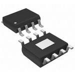
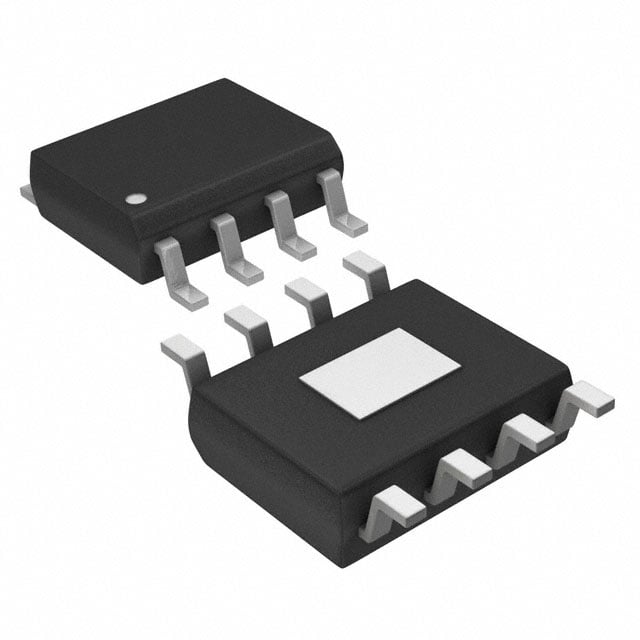
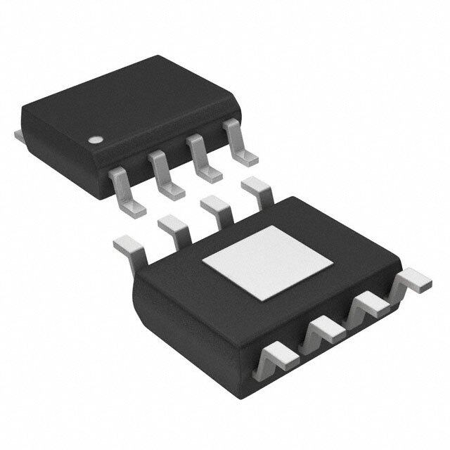
| 产品图片 |
|
| rohs | 符合RoHS无铅 / 符合限制有害物质指令(RoHS)规范要求 |
| 产品系列 | 电源管理 IC,稳压器—开关式稳压器,Texas Instruments TPS5432DDA- |
| 数据手册 | |
| 产品型号 | TPS5432DDA |
| PCN组件/产地 | |
| PCN设计/规格 | |
| PWM类型 | 电流模式 |
| 产品种类 | 稳压器—开关式稳压器 |
| 供应商器件封装 | 8-SO PowerPad |
| 其它名称 | 296-30340-5 |
| 包装 | 管件 |
| 同步整流器 | 是 |
| 商标 | Texas Instruments |
| 安装类型 | 表面贴装 |
| 安装风格 | SMD/SMT |
| 封装 | Tube |
| 封装/外壳 | 8-SOIC(0.154",3.90mm 宽)裸焊盘 |
| 封装/箱体 | HSOP-8 |
| 工作温度 | -40°C ~ 125°C |
| 工作温度范围 | - 40 C to + 125 C |
| 工厂包装数量 | 75 |
| 开关频率 | 700 kHz |
| 拓扑结构 | Buck |
| 最大输入电压 | 6 V |
| 最小工作温度 | - 40 C |
| 标准包装 | 75 |
| 电压-输入 | 2.95 V ~ 6 V |
| 电压-输出 | 0.808 V ~ 4.5 V |
| 电流-输出 | 3A |
| 类型 | Synchronous Step-Down Converter |
| 系列 | TPS5432 |
| 设计资源 | http://www.digikey.com/product-highlights/cn/zh/texas-instruments-webench-design-center/3176 |
| 输出数 | 1 |
| 输出电压 | 1.8 V |
| 输出电流 | 3 A |
| 输出端数量 | 1 Output |
| 输出类型 | 可调式 |
| 配用 | /product-detail/zh/TPS5432EVM-116/296-31195-ND/3431142 |
| 频率-开关 | 700kHz |


- 商务部:美国ITC正式对集成电路等产品启动337调查
- 曝三星4nm工艺存在良率问题 高通将骁龙8 Gen1或转产台积电
- 太阳诱电将投资9.5亿元在常州建新厂生产MLCC 预计2023年完工
- 英特尔发布欧洲新工厂建设计划 深化IDM 2.0 战略
- 台积电先进制程称霸业界 有大客户加持明年业绩稳了
- 达到5530亿美元!SIA预计今年全球半导体销售额将创下新高
- 英特尔拟将自动驾驶子公司Mobileye上市 估值或超500亿美元
- 三星加码芯片和SET,合并消费电子和移动部门,撤换高东真等 CEO
- 三星电子宣布重大人事变动 还合并消费电子和移动部门
- 海关总署:前11个月进口集成电路产品价值2.52万亿元 增长14.8%


PDF Datasheet 数据手册内容提取
TPS5432 www.ti.com SLVSB89A–MARCH2012–REVISEDOCTOBER2012 2.95V to 6V Input, 3A Output, 700kHz Synchronous Step Down Converter CheckforSamples:TPS5432 FEATURES DESCRIPTION 1 • Two70mΩ(typical)MOSFETsfor3A The TPS5432 is a 6V, 3A, low Iq, current mode, 2 synchronous monolithic buck converter with ContinuousOutputCurrent integrated MOSFETs. The TPS5432 enables small • CurrentModeControlWithExternal designs by integrating the MOSFETs, implementing Compensation current mode control to reduce external component • 700kHzSwitchingFrequency count, reducing inductor size by 700kHz switching frequency. SOIC-8 package with exposed thermal • 360µAnoLoadQuiescentOperatingCurrent pad provides both thermally enhanced solution and (noswitching) easytouse. • 0.808VInternalVoltageReference The TPS5432 provides accurate regulation for a • ±2.0%ReferenceAccuracyat25°C variety of loads with an accurate 3.0% voltage • ±3.0%ReferenceAccuracyOverTemperature referenceovertemperature. Range–40°C~125°C Efficiency is maximized through the integrated 70mΩ • StableOperationWithCeramicOutput MOSFETs and 360μA typical supply current. Using Capacitor the enable pin, shutdown supply current is reduced to • AdjustableSlowStart 2µAbyenteringashutdownmode. • CyclebyCycleCurrentLimit,andFrequency The output voltage startup ramp is controlled by the FoldBackProtection slow start pin. A ceramic capacitor at this pin can • ThermallyEnhanced8-PinSOIC(DDA) easilyadjusttheslowstarttime. Package Frequency fold back and thermal shutdown protects thedeviceduringanover-currentcondition. APPLICATIONS • ConsumerApplicationssuchasDTV,SetTop Boxes,LCDdisplays,CPE • Low-VoltagePoint-of-LoadRegulationsfor SoC,CPU,DSP 100 SIMPLIFIED SCHEMATIC 95 INPUT 90 3-6 V 2 VIN 1 CBOOT 85 Cin BOOT % 1100m VF TPS5432 PH 301.01 VmF 3.3LOmH 1.2 V@3A ciency - 8705 C Effi 70 76 EN 5 22mFx2O R101 kW C39ff0 pF 6650 VVViiinnn === 355. 3VV,,V VV,ooVuuottu ==t =11..128. 2VVV COMP VSENSE 55 Vin = 3.3 V, Vout = 1.8 V 4.99 kRWc 8 SS 4 R202 kW 500 500 1000 V1i5n0 =0 5 V2, 0V0o0ut = 32.530 V0 3000 Cc GND Load Current - mA 3.3 nF Css 0.01mF 1 Pleasebeawarethatanimportantnoticeconcerningavailability,standardwarranty,anduseincriticalapplicationsof TexasInstrumentssemiconductorproductsanddisclaimerstheretoappearsattheendofthisdatasheet. PowerPADisatrademarkofTexasInstruments. 2 PRODUCTIONDATAinformationiscurrentasofpublicationdate. Copyright©2012,TexasInstrumentsIncorporated Products conform to specifications per the terms of the Texas Instruments standard warranty. Production processing does not necessarilyincludetestingofallparameters.
TPS5432 SLVSB89A–MARCH2012–REVISEDOCTOBER2012 www.ti.com Thesedeviceshavelimitedbuilt-inESDprotection.Theleadsshouldbeshortedtogetherorthedeviceplacedinconductivefoam duringstorageorhandlingtopreventelectrostaticdamagetotheMOSgates. PIN CONFIGURATION SO-8WITHTHERMALPAD (TOPVIEW) BOOT 1 8 SS VIN 2 7 EN Thermal Pad PH 3 6 COMP GND 4 5 VSENSE PINFUNCTIONS PIN DESCRIPTION NAME NUMBER AbootstrapcapisrequiredbetweenBOOTandPH.Ifthevoltageonthiscapisbelowtheminimum BOOT 1 requiredbytheoutputdevice,theoutputisforcedtoswitchoffuntilthecapisrefreshed. Erroramplifieroutput,andinputtotheoutputswitchcurrentcomparator.Connectfrequencycompensation COMP 6 tothispin. Thispinhasaninternalpullupwhichenablesswitchingifleftopen.Todisableswitchingandreduce EN 7 quiescentcurrent,thispinmustbepulledtoground. GND 4 Ground.ThispinshouldbeelectricallyconnecteddirectlytothethermalpadundertheIC ThesourceoftheinternalhighsidepowerMOSFET,anddrainoftheinternallowside(synchronous) PH 3 rectifierMOSFET. SS 8 Slowstarttimesetting.Anexternalcapacitorconnectedtothispinsetstheoutputrisetime GNDpinshouldbeconnectedtotheexposedthermalpadforproperoperation.Thisthermalpadshould THERMALPAD 9 beconnectedtoanyinternalPCBgroundplaneusingmultipleviasforgoodthermalperformance. VIN 2 Suppliesthecontrolcircuitryandswitchesofthepowerconverter.Therangeis2.95Vto6V. VSENSE 5 Invertingnodeofthegmerroramplifier. ORDERINGINFORMATION(1) T PACKAGE(2) (3) ORDERABLEPARTNUMBER j Tube TPS5432DDA –40°Cto125°C 8-pinSOICPowerPAD™ TapeandReel TPS5432DDAR (1) Forthemostcurrentpackageandorderinginformation,seethePackageOptionAddendumattheendofthisdocument,orseetheTI websiteatwww.ti.com. (2) Packagedrawings,thermaldata,andsymbolizationareavailableatwww.ti.com/packaging. (3) AllpackageoptionshaveCuNIPDAUlead/ballfinish. 2 SubmitDocumentationFeedback Copyright©2012,TexasInstrumentsIncorporated ProductFolderLinks:TPS5432
TPS5432 www.ti.com SLVSB89A–MARCH2012–REVISEDOCTOBER2012 ABSOLUTE MAXIMUM RATING(1) VALUE UNIT MIN MAX VIN –0.3 7 EN –0.3 3.6 BOOT PH+7 Inputvoltage V VSENSE –0.3 3 COMP –0.3 3 SS –0.3 3 BOOT-PH 7 Outputvoltage PH –0.6 7 V PH10nsTransient –2 10 Sourcecurrent EN 100 µA COMP 100 Sinkcurrent µA SS 100 Electrostaticdischarge(HBM)QSS009-105(JESD22-A114A)(2) 2 kV Electrostaticdischarge(CDM)QSS009-147(JESD22-C101B.01) 500 V T –40 150 J Temperature °C T –65 150 stg (1) Stressesbeyondthoselistedunderabsolutemaximumratingsmaycausepermanentdamagetothedevice.Thesearestressratings only,andfunctionaloperationofthedeviceattheseoranyotherconditionsbeyondthoseindicatedunderELECTRICAL SPECIFICATIONSisnotimplied.Exposuretoabsolute-maximum-ratedconditionsforextendedperiodsmayaffectdevicereliability. (2) Thehumanbodymodelisa100-pFcapacitordischargethrougha1.5-kΩresistorintoeachpin.Themachinemodelisa200-pF capacitordischargeddirectlyintoeachpin. THERMAL INFORMATION TPS5432 THERMALMETRIC(1) UNITS DDA(8PINS) θ Junction-to-ambientthermalresistance 42.1 JA θ Junction-to-case(top)thermalresistance 50.9 JCtop θ Junction-to-boardthermalresistance 31.8 JB °C/W ψ Junction-to-topcharacterizationparameter 5 JT ψ Junction-to-boardcharacterizationparameter 13.5 JB θ Junction-to-case(bottom)thermalresistance 7.1 JCbot spacer (1) Formoreinformationabouttraditionalandnewthermalmetrics,seetheICPackageThermalMetricsapplicationreport,SPRA953. spacer Copyright©2012,TexasInstrumentsIncorporated SubmitDocumentationFeedback 3 ProductFolderLinks:TPS5432
TPS5432 SLVSB89A–MARCH2012–REVISEDOCTOBER2012 www.ti.com ELECTRICAL CHARACTERISTICS TheElectricalRatingsspecifiedinthissectionapplytoallspecificationsinthisdocument,unlessotherwisenoted.These specificationsareinterpretedasconditionsthatdonotdegradetheparametricorfunctionalspecificationsofthedeviceforthe lifeoftheproductcontainingit.TestConditions:T =–40°Cto125°C,VIN=2.95to6V,(unlessotherwisenoted) J PARAMETERS CONDITIONS MIN TYP MAX UNIT SUPPLYVOLTAGE Vin 2.95 6 V Iqshutdown EN=0V,25°C,2.95V<Vin<6V 2 5 µA Iqoperating Noload,Vin=5V,noswitching,Vsense=1V,25°C 360 575 µA VINUVLO InputUVLOthreshold RisingVin 2.6 2.8 V InputUVLOhysteresis 0.2 V ENABLE Enablethreshold Rising 0.984 1.23 1.47 V Enablethreshold Falling 0.952 1.19 Enablethreshold+50mv –4.6 Inputcurrent µA Enablethreshold–50mv –1.2 VOLTAGEREFERENCE 2.95V<Vin<6V,TJ=25°C 0.792 0.808 0.824 V Reference 2.95V<Vin<6V,–40°C<TJ<+125°C 0.784 0.808 0.832 V MOSFET H.Sswitchresistance BOOT-PH=5V,TJ=25°C 62 86 mΩ L.Sswitchresistance Vin=5V,TJ=25°C 73 103 mΩ H.Sswitchresistance BOOT-PH=2.95V,TJ=25°C 88 114 mΩ L.Sswitchresistance Vin=2.95V,TJ=25°C 94 128 mΩ ERRORAMPLIFIER Erroramptransconductance(gm) –2µA<ICOMP<2µA,V(COMP)=1V 245 µmho Erroramptransconductance(gm)duringsoftstart –2µA<ICOMP<2µA,V(COMP)=1V,Vsense=0.3V 70 µmho Errorampsource/sink V(COMP)=1V,100mVoverdrive ±20 µA COMPtoIphgm Vin=5V,Iph1=(0.5or1A)andIph2=3A 15 A/V FREQUENCYFOLDBACKvs.VSENSE VsensevoltageforFsfoldback 50%frequency 0.4 V VsensevoltageforFsfoldback 25%frequency 0.2 V CURRENTLIMIT ImaxHighsideFET Vin=3.3V,dutycycle=100% 3.8 5.7 7 A ImaxLowsideFET 0.8 1.8 A THERMALSHUTDOWN ThermalShutdown 155 170 C OTHysteresis 15 C SWITCHINGFREQUENCY Switchingfrequency 520 700 880 kHz PH(PHPIN) Minimumontime Vin=5V;Measuredat50%pointsonPH,Iout=3A 120 150 ns Minimumofftime Priortoskippingoffpulses,BOOT-PH=2.95V,Iout=3A 60 ns Rise/Falltime Vin=5V,Io=0A 1.5 V/ns Rise/Falltime Vin=5V,Io=3A 1.5 V/ns BOOT BootrechargeFETresistance Vin=5V 15 Ω BootUVLO Vin=2.95V 2.1 V SLOWSTARTTIME Chargecurrent Vss=0.4V 2 μA 4 SubmitDocumentationFeedback Copyright©2012,TexasInstrumentsIncorporated ProductFolderLinks:TPS5432
TPS5432 www.ti.com SLVSB89A–MARCH2012–REVISEDOCTOBER2012 TYPICAL CHARACTERISTICS CURVES HIGHSIDE&LOWSIDERdson FREQUENCY vs vs JUNCTIONTEMPERATURE JUNCTIONTEMPERATURE 130 750 We - m120 LSF, VI= 3.3 V VI=5 V stanc110 HSF, VI= 3.3 V kHz 730 Resi100 LSF, VI= 5 V cy - Source On 8900 HSF, VI= 5 V ng Frequen 710 n- hi 690 Drai 70 witc on - Static 5600 f - Ssw 670 s d R 40 650 -50 -25 0 25 50 75 100 125 150 -50 -25 0 25 50 75 100 125 150 TJ- Junction Temperature - °C TJ- Junction Temperature - °C Figure1. Figure2. HIGHSIDECURRENTLIMITTHRESHOLD VOLTAGEREFERENCE vs vs JUNCTIONTEMPERATURE JUNCTIONTEMPERATURE 8 0.840 old -A 7 VI= 3.3 V High Side Current Limit Thresh 456 VIV=I 3=. 35 VV Vref - Voltage Reference - V 00..880200 cI - I 3 0.780 -50 -25 0 25 50 75 100 125 150 -50 -25 0 25 50 75 100 125 150 TJ- Junction Temperature - °C TJ- Junction Temperature - °C Figure3. Figure4. Copyright©2012,TexasInstrumentsIncorporated SubmitDocumentationFeedback 5 ProductFolderLinks:TPS5432
TPS5432 SLVSB89A–MARCH2012–REVISEDOCTOBER2012 www.ti.com TYPICAL CHARACTERISTICS CURVES (continued) SWITCHINGFREQUENCY EATRANSCONDUCTANCE vs vs VSENSE JUNCTIONTEMPERATURE 100 TJ= 25°C 290 VI= 3.3 V ncy - % 75 Vsense Falling Vsense Rising A/Vm270 hing Freque 50 nductance -223500 witc sco minal S 25 A- Tran210 o E N 190 00 0.1 0.2 0.3 0.4 0.5 0.6 0.7 0.8 170-50 -25 0 25 50 75 100 125 150 VSENSE - V TJ- Junction Temperature - °C Figure5. Figure6. EATRANSCONDUCTANCE(SLOWSTART) SLOWSTARTCHARGECURRENT vs vs JUNCTIONTEMPERATURE JUNCTIONTEMPERATURE 105 2.6 VI= 3.3 V 100 95 V A 2.5 EA-Transconductance -A/m 677889505050 I- SS Charge Current -mSS 22..34 60 55 2.2 -50 -25 0 25 50 75 100 125 150 -50 -25 0 25 50 75 100 125 150 TJ- Junction Temperature - °C TJ- Junction Temperature - °C Figure7. Figure8. 6 SubmitDocumentationFeedback Copyright©2012,TexasInstrumentsIncorporated ProductFolderLinks:TPS5432
TPS5432 www.ti.com SLVSB89A–MARCH2012–REVISEDOCTOBER2012 TYPICAL CHARACTERISTICS CURVES (continued) INPUTVOLTAGEUVLOTHRESHOLD SHUTDOWNSUPPLYCURRENT vs vs JUNCTIONTEMPERATURE JUNCTIONTEMPERATURE 2.9 4 VI= 3.3 V; EN = 0 V 2.8 A m VLO Threshold - V 222...567 UVLO StarUt sVwLiOtc hSintogp switching n Quiescent Current - 23 U w V- I2.4 hutdo 1 S - 2.3 Isd 2.2 0 -50 -25 0 25 50 75 100 125 150 -50 -25 0 25 50 75 100 125 150 TJ- Junction Temperature - °C TJ- Junction Temperature - °C Figure9. Figure10. SHUTDOWNSUPPLYCURRENT VINSUPPLYCURRENT vs vs INPUTVOLTAGE JUNCTIONTEMPERATURE 4 420 410 VI= 3.3 V; Vsense= 1 V Current -Am 3 TJ= 25°C; EN = 0 V urrent -Am 349000 cent ply C 380 es 2 up 370 n Qui ent S 360 w c - Shutdod1 vin - Quies 334500 Is I 330 0 320 3 3.5 4 4.5 5 5.5 6 -50 -25 0 25 50 75 100 125 150 VI- Input Voltage - V TJ- Junction Temperature - °C Figure11. Figure12. Copyright©2012,TexasInstrumentsIncorporated SubmitDocumentationFeedback 7 ProductFolderLinks:TPS5432
TPS5432 SLVSB89A–MARCH2012–REVISEDOCTOBER2012 www.ti.com TYPICAL CHARACTERISTICS CURVES (continued) VINSUPPLYCURRENT ENPINUVLOTHRESHOLD vs vs INPUTVOLTAGE JUNCTIONTEMPERATURE 420 1.26 410 TJ= 25°C; Vsense = 1 V 1.25 VI= 3.3 V EN Rising Am 400 1.24 nt - V1.23 Curre 390 old - 1.22 nt Supply 337800 LO Thresh1.12.12 EN Falling e 360 V Quiesc 350 EN - U11..1189 vin - 340 1.17 I 330 1.16 320 1.15 3 3.5 4 4.5 5 5.5 6 -50 -25 0 25 50 75 100 125 150 VI- Input Voltage - V TJ- Junction Temperature - °C Figure13. Figure14. ENPINPULLUPCURRENT ENPINPULLUPCURRENT vs vs JUNCTIONTEMPERATURE JUNCTIONTEMPERATURE 5 1.25 VI= 3.3 V, VI= 3.3 V, 4.9 Ven =Threshold + 50 mV Ven =Threshold - 50 mV 1.225 4.8 A4.7 A m m 1.2 Current -44..56 Current -1.175 Iu - Pullup 44..34 Ip - Pullup 1.15 4.2 1.125 4.1 4 1.1 -50 -25 0 25 50 75 100 125 150 -50 -25 0 25 50 75 100 125 150 TJ- Junction Temperature - °C TJ- Junction Temperature - °C Figure15. Figure16. 8 SubmitDocumentationFeedback Copyright©2012,TexasInstrumentsIncorporated ProductFolderLinks:TPS5432
TPS5432 www.ti.com SLVSB89A–MARCH2012–REVISEDOCTOBER2012 SIMPLIFIED BLOCK DIAGRAM (DDA) EN VIN i i 1 hys Thermal Enable Shutdown UVLO Logic Comparator Shutdown + Shutdown Logic _ 107% Boot Voltage Charge Reference Minimum Boot Clamp UVLO Current Pulse Sense Error Skip Amplifier PWM VSENSE Comparator PWM BOOT Latch Logic R Q SS Logic S Shutdown Logic S Slope Compensation COMP PH Frequency Shift Overload Maximum Recovery Clamp Oscillator TPS5432DDABlock Diagram GND Thermal PAD OVERVIEW The TPS5432 is a 6-V, 3-A, synchronous step-down (buck) converter with two integrated n-channel MOSFETs. To improve performance during line and load transients the device implements a constant frequency, peak current mode control which reduces output capacitance and simplifies external frequency compensation design. The fixed switching frequency of 700kHz provides the balance between efficiency and size of the output filter components. The TPS5432 has a typical default start up voltage of 2.6 V. The EN pin has an internal pull-up current source that can provide a default condition when the EN pin is floating for the device to operate. The total operating current for the TPS5432 is typically 360μA when not switching and under no load. When the device is disabled, thesupplycurrentislessthan5μA. The integrated 70mΩ MOSFETs allow for high efficiency power supply designs with continuous output currents upto3amperes. TheTPS5432reducestheexternalcomponentcountbyintegratingthebootrechargediode.Thebiasvoltagefor the integrated high side MOSFET is supplied by a capacitor between the BOOT and PH pins. The boot capacitor voltage is monitored by an UVLO circuit and turns off the high side MOSFET when the voltage falls below a presetthreshold.Theoutputvoltagecanbesteppeddowntoaslowasthe0.808Vreference. Copyright©2012,TexasInstrumentsIncorporated SubmitDocumentationFeedback 9 ProductFolderLinks:TPS5432
TPS5432 SLVSB89A–MARCH2012–REVISEDOCTOBER2012 www.ti.com The TPS5432 minimizes excessive output over-voltage transients by taking advantage of the over-voltage comparator. When the regulated output voltage is greater than 107% of the nominal voltage, the over-voltage comparator is activated, and the high side MOSFET is turned off and masked from turning on until the output voltageislowerthan105%. The SS (slow start) pin is used to minimize inrush currents during power up. A small value capacitor should be coupled to the pin for slow start. The SS pin is discharged before the output power up to ensure a repeatable restartafteranover-temperaturefault,UVLOfaultordisabledcondition. The use of a frequency fold-back circuit reduces the switching frequency during startup and over current fault conditionstohelplimittheinductorcurrent. DETAILED DESCRIPTION FIXED FREQUENCY PWM CONTROL The TPS5432 uses a fixed frequency, peak current mode control. The output voltage is compared through external resistors on the VSENSE pin to an internal voltage reference by an error amplifier which drives the COMP pin. An internal oscillator initiates the turn on of the high side power switch. The error amplifier output is compared to the high side power switch current. When the power switch current reaches the COMP voltage level the high side power switch is turned off and the low side power switch is turned on. The COMP pin voltage increases and decreases as the output current increases and decreases. The device implements a current limit by clamping the COMP pin voltage to a maximum level and also implements a minimum clamp for improved transientresponseperformance. SLOPE COMPENSATION AND OUTPUT CURRENT The TPS5432 adds a compensating ramp to the switch current signal. This slope compensation prevents sub- harmonic oscillations as duty cycle increases. The available peak inductor current remains constant over the full dutycyclerange. BOOTSTRAP VOLTAGE (BOOT) The TPS5432 has an integrated boot regulator and requires a small ceramic capacitor between the BOOT and PHpintoprovidethegatedrivevoltageforthehighsideMOSFET.Thevalueoftheceramiccapacitorshouldbe 0.1μF. A ceramic capacitor with an X7R or X5R grade dielectric with a voltage rating of 10 V or higher is recommendedbecauseofthestablecharacteristicsovertemperatureandvoltage. The high side MOSFET is turned off using an UVLO circuit, allowing for the low side MOSFET to conduct when thevoltagefromBOOTtoPHdropsbelow2.1V. The device may work at 100% duty ratio as long as the BOOT-PH voltage is higher than the BOOT-PH UVLO threshold; but, do not operate the device at 100% duty ratio with no load. See additional information regarding 100%dutyratiointheENABLEANDUNDERVOLTAGELOCKOUTsection. ERROR AMPLIFIER The TPS5432 has a transconductance amplifier. The error amplifier compares the VSENSE voltage to the lower of the SS pin voltage or the internal 0.808 V voltage reference. The transconductance of the error amplifier is 245μA/V during normal operation. When the voltage of VSENSE pin is below 0.808 V and the device is regulating using the SS voltage, the gm is 70μA/V. The frequency compensation components are placed betweentheCOMPpinandground. VOLTAGE REFERENCE The voltage reference system produces a precise ±3% voltage reference over temperature by scaling the output of a temperature stable bandgap circuit. The bandgap and scaling circuits produce 0.808 V at the non-inverting inputoftheerroramplifier. 10 SubmitDocumentationFeedback Copyright©2012,TexasInstrumentsIncorporated ProductFolderLinks:TPS5432
TPS5432 www.ti.com SLVSB89A–MARCH2012–REVISEDOCTOBER2012 ADJUSTING THE OUTPUT VOLTAGE The output voltage is set with a resistor divider from the output node to the VSENSE pin. It is recommended to use divider resistors with 1% tolerance or better. Start with a 10 kΩ for the R1 resistor, Figure 17, and use the Equation 1 to calculate R2. To improve efficiency at light loads consider using larger value resistors. If the values are too high the regulator is more susceptible to noise and voltage errors from the VSENSE input current are noticeable. TPS5432 V O R1 VSENSE – R2 0.808 V + Figure17. VoltageDividerCircuit V R2 = REF ´ R1 V - V OUT REF (1) ENABLE AND UNDERVOLTAGE LOCKOUT The TPS5432 is disabled when the VIN pin voltage falls below 2.4V. If an application requires a higher under- voltage lockout (UVLO), use the EN pin as shown in Figure 18 to adjust the input voltage UVLO by using two external resistors. The EN pin has an internal pull-up current source that provides the default condition of the TPS5432 operating when the EN pin floats. Once the EN pin voltage exceeds 1.23V, an additional 3.4µA of hysteresis is added. When the EN pin is pulled below 1.19V, the 3.4µA is removed. This additional current facilitatesinputvoltagehysteresis. If the target Vout > 2.4V, it is possible for the IC to work under 100% duty ratio without BOOT-PH voltage > BOOT-PH UVLO threshold satisfied during power up and power down. To avoid this, it is strongly recommended to add a resistor divider (R1 & R2 in Figure 18) at the EN pin to program VIN UVLO at a new threshold that is higherthanVout. TPS5432 VIN ihys 3.4mA R1 i1 1.2mA + EN R2 – Figure18. AdjustableUnderVoltageLockOut æ V ö V ç ENFALLING÷-V START STOP R1= è VENRISING ø æ V ö I ç1- ENFALLING÷+I p h è VENRISING ø (2) Copyright©2012,TexasInstrumentsIncorporated SubmitDocumentationFeedback 11 ProductFolderLinks:TPS5432
TPS5432 SLVSB89A–MARCH2012–REVISEDOCTOBER2012 www.ti.com spacer R1 ´ V R2 = ENFALLING ( ) V - V + R1I + I STOP ENFALLING p h (3) WhereI =3.4µA,I =1.2µA,V =1.23V,V =1.19V h P ENRISING ENFALLING V isthetargetVINUVLOrisingthresholdsetbyENresistors. START V isthetargetVINUVLOfallingthresholdsetbyENresistors. STOP SLOW START PIN The TPS5432 regulates to the lower of the SS pin and the internal reference voltage. A capacitor on the SS pin to ground implements a slow start time. The TPS5432 has an internal pull-up current source of 2 μA which charges the external slow start capacitor. Equation 4 calculates the required slow start capacitor value where TSS is the desired slow start time in ms, ISS is the internal slow start charging current of 2 μA, and Vref is the internalvoltagereferenceof0.808V. If during normal operation, the VIN goes below the UVLO, EN pin pulled below 1.19 V, or a thermal shutdown event occurs, the TPS5432 stops switching and the SS is discharged to 0 volts before reinitiating a powering up sequence. Tss(ms)´Iss(mA) Css(nF)= Vref(V) (4) OVERCURRENT PROTECTION The TPS5432 implements a cycle by cycle current limit. During each switching cycle the high side switch current is compared to the voltage on the COMP pin. When the instantaneous switch current intersects the COMP voltage, the high side switch is turned off. During overcurrent conditions that pull the output voltage low, the error amplifier responds by driving the COMP pin high, increasing the switch current. The error amplifier output is clampedinternally.Thisclampfunctionsasaswitchcurrentlimit. FREQUENCY SHIFT To operate at high switching frequencies and provide protection during overcurrent conditions, the TPS5432 implements a frequency shift. If frequency shift was not implemented, during an overcurrent condition the low side MOSFET may not be turned off long enough to reduce the current in the inductor, causing a current runaway. With frequency shift, during an overcurrent condition the switching frequency is reduced from 100%, then 50%, then 25% as the voltage decreases from 0.808V to 0V on VSENSE pin to allow the low side MOSFET to be off long enough to decrease the current in the inductor. During start-up, the switching frequency increases asthevoltageonVSENSEincreasesfrom0Vto0.808V.SeeFigure5fordetails. REVERSE OVERCURRENT PROTECTION The TPS5432 implements low side current protection by detecting the voltage across the low side MOSFET. When the converter sinks current through its low side FET, the control circuit turns off the low side MOSFET if the reverse current is more than 1.8 A. By implementing this additional protection scheme, the converter is able toprotectitselffromexcessivecurrentduringpowercyclingandstart-upintopre-biasedoutputs. OVERVOLTAGE TRANSIENT PROTECTION The TPS5432 incorporates an overvoltage transient protection (OVTP) circuit to minimize voltage overshoot when recovering from output fault conditions or strong unload transients. The OVTP feature minimizes the output overshoot by implementing a circuit to compare the VSENSE pin voltage to the OVTP threshold which is 107% of the internal voltage reference. If the VSENSE pin voltage is greater than the OVTP threshold, the high side MOSFET is disabled preventing current from flowing to the output and minimizing output overshoot. When the VSENSE voltage drops lower than the OVTP threshold, which is 105% of the internal voltage reference, the high sideMOSFETisallowedtoturnonthenextclockcycle. 12 SubmitDocumentationFeedback Copyright©2012,TexasInstrumentsIncorporated ProductFolderLinks:TPS5432
TPS5432 www.ti.com SLVSB89A–MARCH2012–REVISEDOCTOBER2012 THERMAL SHUTDOWN The device implements an internal thermal shutdown to protect itself if the junction temperature exceeds 170°C. The thermal shutdown forces the device to stop switching when the junction temperature exceeds the thermal trip threshold. Once the die temperature decreases below 155°C, the device reinitiates the power-up sequence bydischargingtheSSpinto0volts.Thethermalshutdownhysteresisis15°C. Copyright©2012,TexasInstrumentsIncorporated SubmitDocumentationFeedback 13 ProductFolderLinks:TPS5432
TPS5432 SLVSB89A–MARCH2012–REVISEDOCTOBER2012 www.ti.com APPLICATION INFORMATION DESIGN GUIDE – STEP-BY-STEP DESIGN PROCEDURE This example details the design of a high frequency switching regulator design using ceramic output capacitors. This design is available as the TPS5432EVM-116 (PWR116) evaluation module (EVM). A few parameters must be known in order to start the design process. These parameters are typically determined on the system level. Forthisexample,westartwiththefollowingknownparameters: OutputVoltage 1.8V TransientResponse0.75Ato2.25Aloadstep(25%to75% ΔVout=6% maximumload) MaximumOutputCurrent 3A InputVoltage 3Vto6V,5Vnominal OutputVoltageRipple <18mVp-p SwitchingFrequency(Fsw) 700kHz The schematic diagram for this design example is shown in Figure 19 . The component reference designators of thisschematicareusedfortheequationsinAPPLICATIONINFORMATION. R4 C6 U1 0.1uF TPS5432DDA 0 L1 2 VIN BOOT 1 2.2uH Vout = 1.8 V, 3-A 7 3 C1 C2 R1 EN PH 8 5 SS VSENS R5 C8 C9 10uF 0.1uF 66.5k C3 4 6 GND COMP PWPD 49.9 22uF 22uF R2 10nF 9 R3 45.3k 4.22k C5 C7 R6 C4 82pF 470pF 10.0k 8.2nF R7 8.06k Figure19. 1.8VOutputPowerSupplyDesignwithAdjustableUVLO OUTPUT INDUCTOR SELECTION The inductor selected works for the entire TPS5432 input voltage range. To calculate the value of the output inductor, use Equation 5. K is a coefficient that represents the amount of inductor ripple current relative to the IND maximum output current. The inductor ripple current is filtered by the output capacitor. Therefore, choosing high inductor ripple currents impacts the selection of the output capacitor since the output capacitor must have a ripple current rating equal to or greater than the inductor ripple current. In general, the inductor ripple value is at thediscretionofthedesigner;however,K isnormallyfrom0.1to0.3forthemajorityofapplications. IND For this design example, use K = 0.3 and the minimum inductor value is calculated to be 2.0 μH. For this IND design, a nearest standard value was chosen: 2.2 μH. For the output filter inductor, it is important that the RMS current and saturation current ratings not be exceeded. The RMS and peak inductor current can be found from Equation7andEquation8. For this design, the RMS inductor current is 3.009 A and the peak inductor current is 3.409 A. The chosen inductor is a TDK SPM6530T-2R2M. It has a saturation current rating 0f 8.4 A (20% inductance loss) and a RMS currentratingof8.2A(40°C.temperaturerise).Theseriesresistanceis17.3mΩtypical. 14 SubmitDocumentationFeedback Copyright©2012,TexasInstrumentsIncorporated ProductFolderLinks:TPS5432
TPS5432 www.ti.com SLVSB89A–MARCH2012–REVISEDOCTOBER2012 The current flowing through the inductor is the inductor ripple current plus the output current. During power up, faults or transient load conditions, the inductor current can increase above the calculated peak inductor current level calculated above. In transient conditions, the inductor current can increase up to the switch current limit of the device. For this reason, the most conservative approach is to specify an inductor with a saturation current ratingequaltoorgreaterthantheswitchcurrentlimitratherthanthepeakinductorcurrent. Vinmax - Vout Vout L1= ´ Io ´ Kind Vinmax ´ ¦sw (5) verticalspacer Vinmax - Vout Vout Iripple= ´ L1 Vinmax ´ ¦sw (6) verticalspacer 2 1 æVo ´ (Vinmax - Vo)ö ILrms = Io2 + ´ ç ÷ 12 è Vinmax ´ L1 ´ ¦sw ø (7) verticalspacer Iripple ILpeak= Iout + 2 (8) OUTPUT CAPACITOR There are three primary considerations for selecting the value of the output capacitor. The output capacitor determines the modulator pole, the output voltage ripple, and how the regulator responds to a large change in loadcurrent.Theoutputcapacitanceneedstobeselectedbasedonthemorestringentofthesethreecriteria. The desired response to a large change in the load current is the first criteria. The output capacitor needs to supply the load with current when the regulator can not. This situation would occur if there are desired hold-up times for the regulator where the output capacitor must hold the output voltage above a certain level for a specified amount of time after the input power is removed. The regulator is temporarily not able to supply sufficient output current if there is a large, fast increase in the current needs of the load such as a transition from no load to full load. The regulator usually needs two or more clock cycles for the control loop to see the change in load current and output voltage and adjust the duty cycle to react to the change. The output capacitor must be sized to supply the extra current to the load until the control loop responds to the load change. The output capacitance must be large enough to supply the difference in current for 2 clock cycles while only allowing a tolerable amount of drop in the output voltage. Equation 9 shows the minimum output capacitance necessary to accomplishthis. For this example, the transient load response is specified as a 6% change in Vout for a load step from 0.75 A (25% load) to 2.25 A (75% load). For this example, ΔIout = 2.25 A - 0.75 A = 1.5 A and ΔVout= 0.06 × 1.8 = 0.108V.Usingthesenumbersgivesaminimumcapacitanceof39.7μF.ThisvaluedoesnottaketheESRofthe output capacitor into account in the output voltage change. For ceramic capacitors, the ESR is usually small enoughtoignoreinthiscalculation. Copyright©2012,TexasInstrumentsIncorporated SubmitDocumentationFeedback 15 ProductFolderLinks:TPS5432
TPS5432 SLVSB89A–MARCH2012–REVISEDOCTOBER2012 www.ti.com Equation 10 calculates the minimum output capacitance needed to meet the output voltage ripple specification. Where fsw is the switching frequency, Vripple is the maximum allowable output voltage ripple, and Iripple is the inductor ripple current. In this case, the maximum output voltage ripple is 18 mV. Under this requirement, Equation10yields8.1uF. verticalspacer 2 ´ DIout Co> ¦sw ´ DVout (9) verticalspacer 1 1 Co> ´ 8 ´ ¦sw Voripple Iripple WhereΔIoutisthechangeinoutputcurrent,fswistheregulatorsswitchingfrequencyandΔVoutisthe allowablechangeintheoutputvoltage. (10) verticalspacer Equation 11 calculates the maximum ESR an output capacitor can have to meet the output voltage ripple specification. Equation 11 indicates the ESR should be less than 22 mΩ. In this case, the ESR of the ceramic capacitorismuchlessthan22mΩ. Additional capacitance de-ratings for aging, temperature and DC bias should be factored in which increases this minimum value. For this example, two 22 μF 10 V X5R ceramic capacitors with 3 mΩ of ESR are used. The estimatedcapacitanceafterderatingis2x22µF=44µF. Capacitors generally have limits to the amount of ripple current they can handle without failing or producing excess heat. An output capacitor that can support the inductor ripple current must be specified. Some capacitor datasheetsspecifytheRMS(RootMeanSquare)valueofthemaximumripplecurrent.Equation12canbeused to calculate the RMS ripple current the output capacitor needs to support. For this application, Equation 12yields 236mA. Voripple Resr< Iripple (11) verticalspacer Vout ´ (Vinmax - Vout) Icorms = 12 ´ Vinmax ´ L1 ´ ¦sw (12) INPUT CAPACITOR The TPS5432 requires a high quality ceramic, type X5R or X7R, input decoupling capacitor of at least 10 μF of effective capacitance and in some applications a bulk capacitance. The effective capacitance includes any DC bias effects. The voltage rating of the input capacitor must be greater than the maximum input voltage. The capacitor must also have a ripple current rating greater than the maximum input current ripple of the TPS5432. TheinputripplecurrentcanbecalculatedusingEquation13. The value of a ceramic capacitor varies significantly over temperature and the amount of DC bias applied to the capacitor. The capacitance variations due to temperature can be minimized by selecting a dielectric material that is stable over temperature. X5R and X7R ceramic dielectrics are usually selected for power regulator capacitors because they have a high capacitance to volume ratio and are fairly stable over temperature. The output capacitor must also be selected with the DC bias taken into account. The capacitance value of a capacitor decreasesastheDCbiasacrossacapacitorincreases. For this example design, a ceramic capacitor with at least a 10 V voltage rating is required to support the maximum input voltage. For this example, one 10 μF and one 0.1 μF 10 V capacitors in parallel have been selected. The input capacitance value determines the input ripple voltage of the regulator. The input voltage ripplecanbecalculatedusingEquation14.Usingthedesignexamplevalues,Ioutmax=3A,Cin=10 μF,Fsw= 700kHz,yieldsaninputvoltagerippleof106mVandarmsinputripplecurrentof1.47A. 16 SubmitDocumentationFeedback Copyright©2012,TexasInstrumentsIncorporated ProductFolderLinks:TPS5432
TPS5432 www.ti.com SLVSB89A–MARCH2012–REVISEDOCTOBER2012 Vout (Vinmin - Vout) Icirms =Iout ´ ´ Vinmin Vinmin (13) verticalspacer Ioutmax ´ 0.25 DVin = Cin ´ ¦sw (14) SLOW START CAPACITOR The slow start capacitor determines the minimum amount of time it takes for the output voltage to reach its nominal programmed value during power up. This is useful if a load requires a controlled voltage slew rate. This is also used if the output capacitance is very large and would require large amounts of current to quickly charge the capacitor to the output voltage level. The large currents necessary to charge the capacitor may make the TPS5432 reach the current limit or excessive current draw from the input power supply may cause the input voltagerailtosag.Limitingtheoutputvoltageslewratesolvesbothoftheseproblems. TheslowstartcapacitorvaluecanbecalculatedusingEquation15.Fortheexamplecircuit,theslowstarttimeis not too critical since the output capacitor value is 2 x 22 μF which does not require much current to charge to 1.8 V. The example circuit has the slow start time set to an arbitrary value of 3.33 ms which requires a 10 nF capacitor. C3(nF)=3×Tss(mS) (15) OUTPUT VOLTAGE AND FEEDBACK RESISTORS SELECTION For the example design, 10.0 kΩ was selected for R6. Using Equation 16, R7 is calculated as 8.15 kΩ. A close standard1%resistoris8.06kΩ. R6×V R7= REF V -V OUT REF (16) TheTPS5432canregulatetooutputvoltagesatorabovetheinternalvoltagereferenceof0.808V.Theoretically, the output voltage may be limited by the minimum controllable on time of the device. For the TPS5432, this should never be an issue as the minimum output voltage of 0.808 V, maximum input voltage of 6 V and the fixed operatingfrequencyof700kHzwillalwaysresultinontimesabovetheminimum. There is also a maximum achievable output voltage which is limited by the minimum off time of 60 nsec typical . For normal operation, that limits the effective duty cycle to 95.8%. The TPS5432 can operate at higher effective duty cycles. In this operating mode, the device will have some switching cycles where the on time is 100% of the cycle. If the output current is increased further at this point, two discreet operating mode will occur sequentially. In the first mode, the device will switch at the normal 700 kHz frequency with the off time at the minimum (60 nsec typical). in the second mode the every alternating switching cycle will be at 100 % on time followed by a cycle with an off time greater than the minimum. The apparent effect is reduction of the operating frequency by 50%. The long term average duty cycle is greater than 95.8%, allowing the device to regulate with input voltages thatapproachtheoutputvoltage. COMPENSATION There are several possible methods to design closed loop compensation for dc/dc converters. For the ideal current mode control, the design equations can be easily simplified. The power stage gain is constant at low frequencies, and rolls off at -20 dB/decade above the modulator pole frequency. The power stage phase is 0 degrees at low frequencies and starts to fall one decade below the modulator pole frequency reaching a minimum of -90 degrees one decade above the modulator pole frequency. The modulator pole is a simple pole showninEquation17. 1 F = PMOD 2×p×C ×R OUT OUT (17) Copyright©2012,TexasInstrumentsIncorporated SubmitDocumentationFeedback 17 ProductFolderLinks:TPS5432
TPS5432 SLVSB89A–MARCH2012–REVISEDOCTOBER2012 www.ti.com For the TPS5432 most circuits will have relatively high amounts of slope compensation. As more slope compensation is applied, the power stage characteristics will deviate from the ideal approximations. The phase loss of the power stage will now approach -180 degrees, making compensation more difficult. The power stage transfer function can be solved but it is a tedious hand calculation that does not lend itself to simple approximations.ItisbesttousePspiceorTINA-TItoaccuratelymodelthepowerstagegainandphasesothata reliable compensation circuit can be designed. That is the technique used in this design procedure. Using the pspice model of SLVM279 apply the values calculated previously to the output filter components of L1, C9 and C10. Set Rload to the appropriate value. For this design, L1 = 2.2 µH. C8 and C9 use the derated capacitance value of 22 µF, and the ESR is set to 3 mΩ. The Rload resistor is 1.8 / 1.5 = 1.2 Ω. Now the power stage characteristiccanbeplottedasshowninFigure20. 50 Gain 150 Phase 40 120 30 90 Gain = 3.25 dB @ 50 kHz 20 60 B) 10 30 d n ( 0 0 Gai −10 −30 −20 −60 −30 −90 −40 −120 −50 −150 −60 −180 100 1000 10000 100000 1000000 Frequency (Hz) G006 Figure20. PowerStageGainandPhaseCharacteristics For this design, the intended crossover frequency is 50 kHz. From the power stage gain and phase plots, the gain at 50 kHz is 3.25 dB and the phase is -128 degrees. For 60 degrees of phase margin, additional phase boost from a feed forward capacitor in parallel with the upper resistor of the voltage set point divider will be required. R3 sets the gain of the compensated error amplifier to be equal and opposite the power stage gain at crossover.TherequiredvalueofR3canbecalculatedfromEquation18. -G PWRSTG 10 20 V R3= × out gm V EA REF (18) To maximize phase gain, the compensator zero F is placed one decade below the crossover frequency F of Z CO 50kHz.TherequiredvalueforC4isgivenbyEquation19. 1 C4= F 2×p×R3× CO 10 (19) To maximize phase gain the high frequency pole F is placed one decade above the crossover frequency F . P CO ThepolecanalsobeusefultooffsettheESRofaluminumelectrolyticoutputcapacitors.ThevalueforC5canbe calculatedfromEquation20. 1 C5= 2×p×R3×F P (20) The feed forward capacitor C7, is used to increase the phase boost at crossover above what is normally available from Type II compensation. It places an additional zero/pole pair located at Equation 21 and Equation22. 1 F = Z 2×p×C7×R6 (21) 1 F = P 2×p×C7×R6PR7 (22) 18 SubmitDocumentationFeedback Copyright©2012,TexasInstrumentsIncorporated ProductFolderLinks:TPS5432
TPS5432 www.ti.com SLVSB89A–MARCH2012–REVISEDOCTOBER2012 This zero and pole pair is not independent. Once the zero location is chosen, the pole is fixed as well. For optimum performance, the zero and pole should be located symmetrically about the intended crossover frequency.TherequiredvalueforC10cancalculatedfromEquation23. 1 C7= V 2×p×R6×F × REF CO V OUT (23) For this design the calculated values for the compensation components are R3 = 4.19 kΩ , C4 = 7596 pF, C5 = 76pFandC7=475pF.Usingstandardvalues,thecompensationcomponentsareR3=4.22kΩ ,C4=8200pF, C5=82pFandC7=470pF. APPLICATION CURVES 100 100 90 90 80 80 70 70 %) %) y ( 60 y ( 60 nc 50 nc 50 e e Effici 40 Effici 40 30 30 20 20 10 VIN = 3.3 V 10 VIN = 3.3 V VIN = 5 V VIN = 5 V 0 0 0 0.5 1 1.5 2 2.5 3 0.001 0.01 0.1 1 10 Output Current (A) Output Current (A) G001 G002 Figure21.EFFICIENCYvsLOADCURRENT Figure22.EFFICIENCYvsLOADCURRENT 60 180 50 Gain 150 Phase V = 100 mV/div (ac coupled) 40 120 OUT 30 90 20 60 Gain (dB) −11000 −03030 Phase (°) Load Current = 1A/div −20 −60 −30 −90 −40 −120 −50 −150 −60 −180 Load step = 0.75Ato 2.25A 100 1000 10000 100000 1000000 Slew rate = 50 mA/ µsec Frequency (Hz) G005 Time = 1 µs/div Figure23.TRANSIENTRESPONSE,1.5ASTEP Figure24.CLOSEDLOOPRESPONSE,V =5V, IN I =1.5A OUT Copyright©2012,TexasInstrumentsIncorporated SubmitDocumentationFeedback 19 ProductFolderLinks:TPS5432
TPS5432 SLVSB89A–MARCH2012–REVISEDOCTOBER2012 www.ti.com V = 5 V/div IN V = 5 V/div IN EN = 2 V/div EN = 2 V/div SS = 2 V/div SS = 2 V/div VOUT= 1 V/div VOUT= 1 V/div Time = 2 ms/div Time = 2 ms/div Figure25.STARTUPRELATIVETOV Figure26.STARTUPRELATIVETOEN IN V = 5 V/div V = 5 V/div IN IN EN = 2 V/div EN = 2 V/div SS = 2 V/div SS = 2 V/div V = 1 V/div V = 1 V/div OUT OUT Time = 2 ms/div Time = 2 ms/div Figure27.SHUTDOWNRELATIVETOV Figure28.SHUTDOWNRELATIVETOEN IN VIN= 200 mV/div (ac coupled) VOUT= 20 mV/div (ac coupled) PH = 2 V/div PH = 2 V/div Time = 1 µs/div Time = 1 µs/div Figure29.INPUTVOLTAGERIPPLE,I =3A Figure30.OUTPUTVOLTAGERIPPLE,I =3A OUT OUT 20 SubmitDocumentationFeedback Copyright©2012,TexasInstrumentsIncorporated ProductFolderLinks:TPS5432
TPS5432 www.ti.com SLVSB89A–MARCH2012–REVISEDOCTOBER2012 LAYOUT Layout is a critical portion of good power supply design. There are several signal paths that conduct fast changing currents or voltages that can interact with stray inductance or parasitic capacitance to generate noise or degrade the power supplies performance. Care should be taken to minimize the loop area formed by the bypass capacitor connections and the VIN pins. See Figure 31 for a PCB layout example. The GND pin should be tied directly to the power pad under the IC. The analog ground trace should be connected to the power groung area at a single point. The power pad should be connected to any internal PCB ground planes using multipleviasdirectlyundertheIC.Additionalviascanbeusedtoconnectthetopsidegroundareatotheinternal planes near the input and output capacitors. For operation at full rated load, the top side ground area along with anyadditionalinternalgroundplanesmustprovideadequateheatdissipatingarea. LocatetheinputbypasscapacitorasclosetotheICaspossible. For two-layer board usage, VIN cap C1 should be very close to IC. The total routing distance to Vin and PGND pinscombined<5mm.(RefertoEVMlayout). The PH pin should be routed to the output inductor. Since the PH connection is the switching node, the output inductor should be located very close to the PH pins, and the area of the PCB conductor minimized to prevent excessive capacitive coupling. The boot capacitor must also be located close to the device. To facilitate routing, the connection trace may be located on the back side or internal layer of the PCB. The sensitive analog ground connections for the feedback voltage divider, compensation components and slow start capacitor should be connected to a separate analog ground trace as shown. The additional external components can be placed approximately as shown. It may be possible to obtain acceptable performance with alternate PCB layouts, howeverthislayouthasbeenshowntoproducegoodresultsandismeantasaguideline. Copyright©2012,TexasInstrumentsIncorporated SubmitDocumentationFeedback 21 ProductFolderLinks:TPS5432
TPS5432 SLVSB89A–MARCH2012–REVISEDOCTOBER2012 www.ti.com VIA to Power Ground Plane VIA to Internal or Bottom Layer Connection VIN BOOTtrace on internal or HIGH FREQENCY bottom layer EXPOSED BYPASS THERMALPAD CAPACITOR AREA ANALOG VIN GROUND TRACE SLOW START VIN CAP BOOT SS INPUT BYPASS TO ENABLE VIN EN CAPACITOR CONTROL BOOST PH COMP CAPACITOR GND VSENSE POWER OUTPUT INDUCTOR GROUND FEEDBACK RESISTORS OUTPUT VOUT FILTER Connection to CAPACITORS POWER GROUND on internal or bottom layer Figure31. PCBLayoutExample 22 SubmitDocumentationFeedback Copyright©2012,TexasInstrumentsIncorporated ProductFolderLinks:TPS5432
TPS5432 www.ti.com SLVSB89A–MARCH2012–REVISEDOCTOBER2012 REVISION HISTORY Note:Pagenumbersofcurrentversionmaydifferfrompreviousversions. ChangesfromOriginal(March2012)toRevisionA Page • Changedlowertemperaturerangefrom–20°Cto–40°CintheReferenceAccuracyOverTemperaturebullet ................. 1 • ChangedESDHBMspecfrom1kVto2kV ........................................................................................................................ 3 • ChangedtemperatureintheconditionsstatementforVoltageReferencespecfrom–20°to–40°C .................................. 4 • ChangedL.SSwitchresistancespecMAXvaluefrom96to103mΩ,forV =5V ........................................................... 4 IN • ChangedL.SSwitchresistancespecMAXvaluefrom126to128mΩ,forV =2.95V .................................................... 4 IN • ChangedImaxLowsideFETCurrentLimitMINvaluefrom1to0.8AandMAXvaluefrom2to1.8A .............................. 4 • AddedsecondparagraphtoENABLEANDUNDERVOLTAGELOCKOUTsection.......................................................... 11 • AddedI =1.2µAto"Where"statementforEquation3 .................................................................................................... 12 P • Changedtemperaturevaluefrom175°Cto170°Cand160°Cto155°CintheTHERMALSHUTDOWNdescription. ..... 13 Copyright©2012,TexasInstrumentsIncorporated SubmitDocumentationFeedback 23 ProductFolderLinks:TPS5432
PACKAGE OPTION ADDENDUM www.ti.com 6-Feb-2020 PACKAGING INFORMATION Orderable Device Status Package Type Package Pins Package Eco Plan Lead/Ball Finish MSL Peak Temp Op Temp (°C) Device Marking Samples (1) Drawing Qty (2) (6) (3) (4/5) TPS5432DDA ACTIVE SO PowerPAD DDA 8 75 Green (RoHS SN Level-2-260C-1 YEAR -40 to 125 5432 & no Sb/Br) TPS5432DDAR ACTIVE SO PowerPAD DDA 8 2500 Green (RoHS SN Level-2-260C-1 YEAR -40 to 125 5432 & no Sb/Br) (1) The marketing status values are defined as follows: ACTIVE: Product device recommended for new designs. LIFEBUY: TI has announced that the device will be discontinued, and a lifetime-buy period is in effect. NRND: Not recommended for new designs. Device is in production to support existing customers, but TI does not recommend using this part in a new design. PREVIEW: Device has been announced but is not in production. Samples may or may not be available. OBSOLETE: TI has discontinued the production of the device. (2) RoHS: TI defines "RoHS" to mean semiconductor products that are compliant with the current EU RoHS requirements for all 10 RoHS substances, including the requirement that RoHS substance do not exceed 0.1% by weight in homogeneous materials. Where designed to be soldered at high temperatures, "RoHS" products are suitable for use in specified lead-free processes. TI may reference these types of products as "Pb-Free". RoHS Exempt: TI defines "RoHS Exempt" to mean products that contain lead but are compliant with EU RoHS pursuant to a specific EU RoHS exemption. Green: TI defines "Green" to mean the content of Chlorine (Cl) and Bromine (Br) based flame retardants meet JS709B low halogen requirements of <=1000ppm threshold. Antimony trioxide based flame retardants must also meet the <=1000ppm threshold requirement. (3) MSL, Peak Temp. - The Moisture Sensitivity Level rating according to the JEDEC industry standard classifications, and peak solder temperature. (4) There may be additional marking, which relates to the logo, the lot trace code information, or the environmental category on the device. (5) Multiple Device Markings will be inside parentheses. Only one Device Marking contained in parentheses and separated by a "~" will appear on a device. If a line is indented then it is a continuation of the previous line and the two combined represent the entire Device Marking for that device. (6) Lead/Ball Finish - Orderable Devices may have multiple material finish options. Finish options are separated by a vertical ruled line. Lead/Ball Finish values may wrap to two lines if the finish value exceeds the maximum column width. Important Information and Disclaimer:The information provided on this page represents TI's knowledge and belief as of the date that it is provided. TI bases its knowledge and belief on information provided by third parties, and makes no representation or warranty as to the accuracy of such information. Efforts are underway to better integrate information from third parties. TI has taken and continues to take reasonable steps to provide representative and accurate information but may not have conducted destructive testing or chemical analysis on incoming materials and chemicals. TI and TI suppliers consider certain information to be proprietary, and thus CAS numbers and other limited information may not be available for release. In no event shall TI's liability arising out of such information exceed the total purchase price of the TI part(s) at issue in this document sold by TI to Customer on an annual basis. Addendum-Page 1
PACKAGE OPTION ADDENDUM www.ti.com 6-Feb-2020 Addendum-Page 2
PACKAGE MATERIALS INFORMATION www.ti.com 17-Jul-2020 TAPE AND REEL INFORMATION *Alldimensionsarenominal Device Package Package Pins SPQ Reel Reel A0 B0 K0 P1 W Pin1 Type Drawing Diameter Width (mm) (mm) (mm) (mm) (mm) Quadrant (mm) W1(mm) TPS5432DDAR SO DDA 8 2500 330.0 12.8 6.4 5.2 2.1 8.0 12.0 Q1 Power PAD PackMaterials-Page1
PACKAGE MATERIALS INFORMATION www.ti.com 17-Jul-2020 *Alldimensionsarenominal Device PackageType PackageDrawing Pins SPQ Length(mm) Width(mm) Height(mm) TPS5432DDAR SOPowerPAD DDA 8 2500 366.0 364.0 50.0 PackMaterials-Page2
GENERIC PACKAGE VIEW DDA 8 PowerPAD TM SOIC - 1.7 mm max height PLASTIC SMALL OUTLINE Images above are just a representation of the package family, actual package may vary. Refer to the product data sheet for package details. 4202561/G
None
None
None
IMPORTANTNOTICEANDDISCLAIMER TI PROVIDES TECHNICAL AND RELIABILITY DATA (INCLUDING DATASHEETS), DESIGN RESOURCES (INCLUDING REFERENCE DESIGNS), APPLICATION OR OTHER DESIGN ADVICE, WEB TOOLS, SAFETY INFORMATION, AND OTHER RESOURCES “AS IS” AND WITH ALL FAULTS, AND DISCLAIMS ALL WARRANTIES, EXPRESS AND IMPLIED, INCLUDING WITHOUT LIMITATION ANY IMPLIED WARRANTIES OF MERCHANTABILITY, FITNESS FOR A PARTICULAR PURPOSE OR NON-INFRINGEMENT OF THIRD PARTY INTELLECTUAL PROPERTY RIGHTS. These resources are intended for skilled developers designing with TI products. You are solely responsible for (1) selecting the appropriate TI products for your application, (2) designing, validating and testing your application, and (3) ensuring your application meets applicable standards, and any other safety, security, or other requirements. These resources are subject to change without notice. TI grants you permission to use these resources only for development of an application that uses the TI products described in the resource. Other reproduction and display of these resources is prohibited. No license is granted to any other TI intellectual property right or to any third party intellectual property right. TI disclaims responsibility for, and you will fully indemnify TI and its representatives against, any claims, damages, costs, losses, and liabilities arising out of your use of these resources. TI’s products are provided subject to TI’s Terms of Sale (www.ti.com/legal/termsofsale.html) or other applicable terms available either on ti.com or provided in conjunction with such TI products. TI’s provision of these resources does not expand or otherwise alter TI’s applicable warranties or warranty disclaimers for TI products. Mailing Address: Texas Instruments, Post Office Box 655303, Dallas, Texas 75265 Copyright © 2020, Texas Instruments Incorporated