ICGOO在线商城 > 集成电路(IC) > PMIC - 稳压器 - DC DC 开关稳压器 > TPS54315PWP
 Datasheet下载
- 型号: TPS54315PWP
- 制造商: Texas Instruments
- 库位|库存: xxxx|xxxx
- 要求:
| 数量阶梯 | 香港交货 | 国内含税 |
| +xxxx | $xxxx | ¥xxxx |
查看当月历史价格
查看今年历史价格
TPS54315PWP产品简介:
ICGOO电子元器件商城为您提供TPS54315PWP由Texas Instruments设计生产,在icgoo商城现货销售,并且可以通过原厂、代理商等渠道进行代购。 TPS54315PWP价格参考¥19.20-¥35.84。Texas InstrumentsTPS54315PWP封装/规格:PMIC - 稳压器 - DC DC 开关稳压器, 固定 降压 开关稳压器 IC 正 2.5V 1 输出 3A 20-PowerTSSOP(0.173",4.40mm 宽)。您可以下载TPS54315PWP参考资料、Datasheet数据手册功能说明书,资料中有TPS54315PWP 详细功能的应用电路图电压和使用方法及教程。
| 参数 | 数值 |
| 产品目录 | 集成电路 (IC)半导体 |
| 描述 | IC REG BUCK SYNC 2.5V 20HTSSOP稳压器—开关式稳压器 Lo-In Voltage 3A Sync Buck Converter |
| 产品分类 | |
| 品牌 | Texas Instruments |
| 产品手册 | |
| 产品图片 |
|
| rohs | 符合RoHS无铅 / 符合限制有害物质指令(RoHS)规范要求 |
| 产品系列 | 电源管理 IC,稳压器—开关式稳压器,Texas Instruments TPS54315PWPSWIFT™ |
| 数据手册 | |
| 产品型号 | TPS54315PWP |
| PWM类型 | 电压模式 |
| 产品培训模块 | http://www.digikey.cn/PTM/IndividualPTM.page?site=cn&lang=zhs&ptm=16804 |
| 产品目录页面 | |
| 产品种类 | 稳压器—开关式稳压器 |
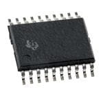
| 供应商器件封装 | 20-HTSSOP |
| 其它名称 | 296-12683-5 |
| 制造商产品页 | http://www.ti.com/general/docs/suppproductinfo.tsp?distId=10&orderablePartNumber=TPS54315PWP |
| 包装 | 管件 |
| 单位重量 | 81.800 mg |
| 同步整流器 | 是 |
| 商标 | Texas Instruments |
| 安装类型 | 表面贴装 |
| 安装风格 | SMD/SMT |
| 宽度 | 4.4 mm |
| 封装 | Tube |
| 封装/外壳 | 20-TSSOP(0.173",4.40mm 宽)裸焊盘 |
| 封装/箱体 | HTSSOP-20 |
| 工作温度 | -40°C ~ 85°C |
| 工作温度范围 | - 40 C to + 85 C |
| 工厂包装数量 | 70 |
| 开关频率 | 700 kHz |
| 拓扑结构 | Buck |
| 最大工作温度 | + 85 C |
| 最大输入电压 | 6 V |
| 最小工作温度 | - 40 C |
| 最小输入电压 | 3 V |
| 标准包装 | 70 |
| 电压-输入 | 3 V ~ 6 V |
| 电压-输出 | 2.5V |
| 电流-输出 | 3A |
| 类型 | 降压(降压) |
| 系列 | TPS54315 |
| 设计资源 | http://www.digikey.com/product-highlights/cn/zh/texas-instruments-webench-design-center/3176 |
| 负载调节 | 0.21 % / A |
| 输入电压 | 3 V to 6 V |
| 输出数 | 1 |
| 输出电压 | 2.5 V |
| 输出电流 | 3 A |
| 输出端数量 | 1 Output |
| 输出类型 | 固定 |
| 频率-开关 | 350kHz,550kHz |


- 商务部:美国ITC正式对集成电路等产品启动337调查
- 曝三星4nm工艺存在良率问题 高通将骁龙8 Gen1或转产台积电
- 太阳诱电将投资9.5亿元在常州建新厂生产MLCC 预计2023年完工
- 英特尔发布欧洲新工厂建设计划 深化IDM 2.0 战略
- 台积电先进制程称霸业界 有大客户加持明年业绩稳了
- 达到5530亿美元!SIA预计今年全球半导体销售额将创下新高
- 英特尔拟将自动驾驶子公司Mobileye上市 估值或超500亿美元
- 三星加码芯片和SET,合并消费电子和移动部门,撤换高东真等 CEO
- 三星电子宣布重大人事变动 还合并消费电子和移动部门
- 海关总署:前11个月进口集成电路产品价值2.52万亿元 增长14.8%


PDF Datasheet 数据手册内容提取
Product Sample & Technical Tools & Support & Folder Buy Documents Software Community TPS54311,TPS54312,TPS54313 TPS54314,TPS54315,TPS54316 SLVS416C–FEBRUARY2002–REVISEDJANUARY2015 TPS5431x 3-V to 6-V Input, 3-A Output Synchronous Buck PWM Switcher With Integrated FETs (SWIFT™) 1 Features 3 Description • 60-mΩ,MOSFETSwitchesforHighEfficiencyat As members of the SWIFT™ family of DC - DC 1 regulators, the TPS54311, TPS54312, TPS54313, 3-AContinuousOutputSourceandSinkCurrent TPS54314, TPS54315 and TPS54316 low-input- • 0.9-V,1.2-V,1.5-V,1.8-V,2.5-V,and3.3-VFixed voltage high-outputcurrent synchronous-buck PWM OutputVoltageDevicesWith1.0%InitialAccuracy converters integrate all required active components. • InternallyCompensatedforLowPartsCount Included on the substrate with the listed features are a true, high performance, voltage error amplifier that • FastTransientResponse provideshighperformanceundertransientconditions; • WidePWMFrequency− Fixed350kHz,550kHz an undervoltage-lockout circuit to prevent start-up orAdjustable280kHzto700kHz until the input voltage reaches 3 V; an internally and • LoadProtectedbyPeakCurrentLimitand externally set slow-start circuit to limit in-rush ThermalShutdown currents; and a powergood output useful for processor/logic reset, fault signaling, and supply • IntegratedSolutionReducesBoardAreaand sequencing. TotalCost The TPS54311, TPS54312, TPS54313, TPS54314, 2 Applications TPS54315 and TPS54316 devices are available in a thermally enhanced 20-pin HTSSOP (PWP) • Low-Voltage,High-DensitySystemsWithPower PowerPAD™ package, which eliminates bulky Distributedat5Vor3.3V heatsinks. TI provides evaluation modules and the • PointofLoadRegulationforHighPerformance SWIFT designer software tool to aid in quickly DSPs,FPGAs,ASICsandMicroprocessors achieving high-performance power supply designs to meetaggressiveequipmentdevelopmentcycles. • Broadband,NetworkingandOptical CommunicationsInfrastructure DeviceInformation(1) • PortableComputing/NotebookPCs PARTNUMBER PACKAGE OUTPUTVOLTAGE TPS54311 0.9V TPS54312 1.2V TPS54313 1.5V HTSSOP(20) TPS54314 1.8V TPS54315 2.5V TPS54316 3.3V (1) For all available packages, see the orderable addendum at theendofthedatasheet. SimplifiedSchematic EfficiencyvsLoadCurrent Input VIN PH Output 96 TPS54316 94 BOOT 92 PGND VBIAS % 90 VSENSE − y c 88 GND n e ci Effi 86 84 TA=25°C 82 VI=5V VO=3.3V 80 0 0.5 1 1.5 2 2.5 3 LoadCurrent−A 1 An IMPORTANT NOTICE at the end of this data sheet addresses availability, warranty, changes, use in safety-critical applications, intellectualpropertymattersandotherimportantdisclaimers.PRODUCTIONDATA.
TPS54311,TPS54312,TPS54313 TPS54314,TPS54315,TPS54316 SLVS416C–FEBRUARY2002–REVISEDJANUARY2015 www.ti.com Table of Contents 1 Features.................................................................. 1 7.4 DeviceFunctionalModes........................................12 2 Applications........................................................... 1 8 ApplicationandImplementation........................ 13 3 Description............................................................. 1 8.1 ApplicationInformation............................................13 4 RevisionHistory..................................................... 2 8.2 TypicalApplication .................................................13 5 PinConfigurationandFunctions......................... 3 9 PowerSupplyRecommendations...................... 16 6 Specifications......................................................... 4 10 Layout................................................................... 16 6.1 AbsoluteMaximumRatings......................................4 10.1 LayoutGuidelines.................................................16 6.2 RecommendedOperatingConditions.......................4 10.2 LayoutExample....................................................17 6.3 ThermalInformation..................................................4 10.3 ThermalConsiderations........................................17 6.4 DissipationRatings...................................................4 11 DeviceandDocumentationSupport................. 18 6.5 ElectricalCharacteristics...........................................5 11.1 DocumentationSupport........................................18 6.6 TypicalCharacteristics..............................................7 11.2 RelatedLinks........................................................18 7 DetailedDescription.............................................. 9 11.3 Trademarks...........................................................18 7.1 Overview...................................................................9 11.4 ElectrostaticDischargeCaution............................18 7.2 FunctionalBlockDiagram.........................................9 11.5 Glossary................................................................18 7.3 FeatureDescription...................................................9 12 Mechanical,Packaging,andOrderable Information........................................................... 18 4 Revision History ChangesfromRevisionB(April2005)toRevisionC Page • AddedFeatureDescriptionsection,DeviceFunctionalModes,ApplicationandImplementationsection,Power SupplyRecommendationssection,Layoutsection,DeviceandDocumentationSupportsection,andMechanical, Packaging,andOrderableInformationsection. .................................................................................................................... 1 2 SubmitDocumentationFeedback Copyright©2002–2015,TexasInstrumentsIncorporated ProductFolderLinks:TPS54311 TPS54312 TPS54313TPS54314 TPS54315 TPS54316
TPS54311,TPS54312,TPS54313 TPS54314,TPS54315,TPS54316 www.ti.com SLVS416C–FEBRUARY2002–REVISEDJANUARY2015 5 Pin Configuration and Functions PWPPackage 20-PinHTSSOP TopView AGND 1 20 RT VSENSE 2 19 FSEL NC 3 18 SS/ENA PWRGD 4 17 VBIAS BOOT 5 16 VIN PH 6 15 VIN PH 7 14 VIN PH 8 13 PGND PH 9 12 PGND PH 10 11 PGND NC–Nointernalconnection PinFunctions PIN DESCRIPTION NAME NO. AGND 1 Analogground.Returnforcompensationnetwork/outputdivider,slow-startcapacitor,VBIAScapacitor,RTresistorandFSELpin.Make PowerPADconnectiontoAGND. BOOT 5 Bootstrapinput.0.022-µFto0.1-µFlow-ESRcapacitorconnectedfromBOOTtoPHgeneratesfloatingdriveforthehigh-sideFETdriver. FSEL 19 Frequencyselectinput.Provideslogicinputtoselectbetweentwointernallysetswitchingfrequencies. NC 3 Noconnection PGND 11−13 Powerground.Highcurrentreturnforthelow-sidedriverandpowerMOSFET.ConnectPGNDwithlargecopperareastotheinputand outputsupplyreturns,andnegativeterminalsoftheinputandoutputcapacitors. PH 6−10 Phaseinput/output.Junctionoftheinternalhighandlow-sidepowerMOSFETs,andoutputinductor. PWRGD 4 Powergoodopen-drainoutput.Hi-ZwhenVSENSE≥90%Vref,otherwisePWRGDislow.NotethatoutputislowwhenSS/ENAislowor internalshutdownsignalactive. RT 20 Frequencysettingresistorinput.ConnectaresistorfromRTtoAGNDtosettheswitchingfrequency,fs. SS/ENA 18 Slow-start/enableinput/output.Dualfunctionpinwhichprovideslogicinputtoenable/disabledeviceoperationandcapacitorinputto externallysetthestart-uptime. VBIAS 17 Internalbiasregulatoroutput.Suppliesregulatedvoltagetointernalcircuitry.BypassVBIASpintoAGNDpinwithahighquality,low ESR0.1-µFto1.0-µFceramiccapacitor. VIN 14−16 InputsupplyforthepowerMOSFETswitchesandinternalbiasregulator.BypassVINpinstoPGNDpinsclosetodevicepackagewitha highquality,lowESR1-µFto10-µFceramiccapacitor. VSENSE 2 Erroramplifierinvertinginput.Connectdirectlytooutputvoltagesensepoint. Copyright©2002–2015,TexasInstrumentsIncorporated SubmitDocumentationFeedback 3 ProductFolderLinks:TPS54311 TPS54312 TPS54313TPS54314 TPS54315 TPS54316
TPS54311,TPS54312,TPS54313 TPS54314,TPS54315,TPS54316 SLVS416C–FEBRUARY2002–REVISEDJANUARY2015 www.ti.com 6 Specifications 6.1 Absolute Maximum Ratings overoperatingfree-airtemperaturerange(unlessotherwisenoted)(1) MIN MAX UNIT VIN,SS/ENA,SYNC −0.3 7 V RT −0.3 6 V V Inputvoltage I VSENSE −0.3 4 V BOOT −0.3 17 V VBIAS,PWRGD,COMP −0.3 7 V V Outputvoltage O PH −0.6 10 V PH InternallyLimited V I Sourcecurrent O COMP,VBIAS 6 mA PH 6 A I Sinkcurrent COMP 6 mA S SS/ENA,PWRGD 10 mA Voltagedifferential AGNDtoPGND ±0.3 V T Operatingvirtualjunctiontemperature –40 125 °C J T Storagetemperature −65 150 °C stg (1) StressesbeyondthoselistedunderAbsoluteMaximumRatingsmaycausepermanentdamagetothedevice.Thesearestressratings only,whichdonotimplyfunctionaloperationofthedeviceattheseoranyotherconditionsbeyondthoseindicatedunderRecommended OperatingConditions.Exposuretoabsolute-maximum-ratedconditionsforextendedperiodsmayaffectdevicereliability. 6.2 Recommended Operating Conditions overoperatingfree-airtemperaturerange(unlessotherwisenoted) MIN MAX UNIT V Inputvoltagerange 3 6 V I T Operatingjunctiontemperature –40 125 °C J 6.3 Thermal Information(1) TPS5431x THERMALMETRIC(2) UNIT PWP(28PINS) R Junction-to-ambientthermalresistance 26.0 θJA °C/W Junction-to-ambientthermalresistance(withoutsolderonPowerPad) 57.5 (1) Testboardconditions: (a) 3inches×3inches,2layers,Thickness0.062inch (b)1.5ozcoppertraceslocatedonthetopofthePCB (c)1.5ozcopperplaneonthebottomofthePCB (d)Tenthermalvias(seerecommendedlandpattern) (2) Formoreinformationabouttraditionalandnewthermalmetrics,seetheICPackageThermalMetricsapplicationreport,SPRA953. 6.4 Dissipation Ratings(1)(2) T =25°C T =70°C T =85°C PACKAGE A A A UNIT POWERRATING POWERRATING POWERRATING 20-PinPWPwithsolder 3.85(3) 2.12 1.54 W 20-pinPWPwithoutsolder 1.73 0.96 0.69 W (1) FormoreinformationonthePWPpackage,refertoTItechnicalbrief,SLMA002 (2) Testboardconditions: (a) 3inches×3inches,2layers,Thickness0.062inch (b)1.5ozcoppertraceslocatedonthetopofthePCB (c)1.5ozcopperplaneonthebottomofthePCB (d)Tenthermalvias(seerecommendedlandpattern) (3) Maximumpowerdissipationmaybelimitedbyovercurrentprotection 4 SubmitDocumentationFeedback Copyright©2002–2015,TexasInstrumentsIncorporated ProductFolderLinks:TPS54311 TPS54312 TPS54313TPS54314 TPS54315 TPS54316
TPS54311,TPS54312,TPS54313 TPS54314,TPS54315,TPS54316 www.ti.com SLVS416C–FEBRUARY2002–REVISEDJANUARY2015 6.5 Electrical Characteristics T =–40°Cto125°C,VIN=3Vto6V(unlessotherwisenoted) J PARAMETER TESTCONDITIONS MIN TYP MAX UNIT SUPPLYVOLTAGE,VIN VIN Inputvoltagerange 3 6 V f =350kHz,FSEL≤0.8V,RTopen 6.2 9.6 s I Quiescentcurrent f =550kHz,FSEL≤2.5V,RTopen,Phasepinopen 8.4 12.8 mA (Q) s Shutdown,SS/ENA=0V 1 1.4 UNDERVOLTAGELOCKOUT Startthresholdvoltage 2.95 3.0 V Stopthresholdvoltage 2.70 2.80 V UVLO Hysteresisvoltage 0.14 0.16 V Risingandfallingedgedeglitch (1) 2.5 µs BIASVOLTAGE Outputvoltage I =0 2.70 2.80 2.90 V (VBIAS) VBIAS Outputcurrent(2) 100 µA OUTPUTVOLTAGE T =25°C,VIN=5V 0.9 J TPS54311 V 3V≤VIN≤6V,0≤I ≤3A,−40°C≤T ≤125°C –2.5% 2.5% L J T =25°C,VIN=5V 1.2 J TPS54312 V 3V≤VIN≤6V,0≤I ≤3A,−40°C≤T ≤125°C –2.5% 2.5% L J T =25°C,VIN=5V 1.5 J TPS54313 V 3V≤VIN≤6V,0≤I ≤3A,−40°C≤T ≤125°C –2.5% 2.5% L J V Outputvoltage O T =25°C,VIN=5V 1.8 J TPS54314 V 3V≤VIN≤6V,0≤I ≤3A,−40°C≤T ≤125°C –2.5% 2.5% L J T =25°C,VIN=5V 2.5 J TPS54315 V 3V≤VIN≤6V,0≤I ≤3A,−40°≤T ≤125°C –2.5% 2.5% L J T =25°C,VIN=5V 3.3 J TPS54316 V 4V≤VIN≤6V,0≤I ≤3A,−40°≤T ≤125°C −2.5% 2.5% L J REGULATION Lineregulation(1)(3) I =3A,350≤fs≤550kHz,T =85°C 0.21 %/V L J Loadregulation(1)(3) I =0Ato3A,350≤f ≤550kHz,T =85°C 0.21 %/A L s J OSCILLATOR FSEL≤0.8V,RTopen 280 350 420 Internallyset-freerunningfrequency kHz FSEL≥2.5V,RTopen 440 550 660 RT=180kΩ(1%resistortoAGND)(1) 252 280 308 Externallyset-freerunning RT=100kΩ(1%resistortoAGND) 460 500 540 kHz frequencyrange RT=68kΩ(1%resistortoAGND)(1) 663 700 762 Highlevelthresholdvoltageat 2.5 V FSEL LowlevelthresholdvoltageatFSEL 0.8 V Rampvalley(1) 0.75 V Rampamplitude(peak-to-peak)(1) 1 V Minimumcontrollableontime(1) 200 ns Maximumdutycycle(1) 90% (1) Specifiedbydesign (2) Staticresistiveloadsonly (3) SpecifiedbythecircuitusedinFigure10. Copyright©2002–2015,TexasInstrumentsIncorporated SubmitDocumentationFeedback 5 ProductFolderLinks:TPS54311 TPS54312 TPS54313TPS54314 TPS54315 TPS54316
TPS54311,TPS54312,TPS54313 TPS54314,TPS54315,TPS54316 SLVS416C–FEBRUARY2002–REVISEDJANUARY2015 www.ti.com Electrical Characteristics (continued) T =–40°Cto125°C,VIN=3Vto6V(unlessotherwisenoted) J PARAMETER TESTCONDITIONS MIN TYP MAX UNIT ERRORAMPLIFIER Erroramplifieropenloopvoltage gain(4) 26 dB Erroramplifierunitygain bandwidth(4) 3 5 MHz PWMCOMPARATOR PWMcomparatorpropagationdelay time,PWMcomparatorinputtoPH 10-mVoverdrive(4) 70 85 ns pin(excludingdeadtime) SLOW-START/ENABLE Enablethresholdvoltage,SS/ENA 0.82 1.20 1.40 V Enablehysteresisvoltage, SS/ENA(4) 0.03 V Fallingedgedeglitch,SS/ENA(4) 2.5 µs TPS54311 2.6 3.3 4.1 TPS54312 3.5 4.5 5.4 Internalslow-start TPS54313 4.4 5.6 6.7 time(4) TPS54314 2.6 3.3 4.1 ms TPS54315 3.6 4.7 5.6 TPS54316 4.7 6.1 7.6 Chargecurrent,SS/ENA SS/ENA=0V 3 5 8 µA Dischargecurrent,SS/ENA SS/ENA=0.2V,V =1.5V 1.5 2.3 4 mA I POWERGOOD Powergoodthresholdvoltage VSENSEfalling 90 %V ref Powergoodhysteresisvoltage(4) 3 %V ref Powergoodfallingedgedeglitch(4) 35 µs Outputsaturationvoltage,PWRGD I =2.5mA 0.18 0.30 V (sink) Leakagecurrent,PWRGD V =5.5V 1 µA I CURRENTLIMIT V =3V,outputshorted(4) 42 6.5 I Currentlimit A V =6V,outputshorted(4) 4.5 7.5 I Currentlimitleadingedgeblanking time(4) 100 ns Currentlimittotalresponsetime(4) 200 ns THERMALSHUTDOWN Thermalshutdowntrippoint(4) 135 150 165 °C Thermalshutdownhysteresis(4) 10 OUTPUTPOWERMOSFETS V =6V(5) 59 88 I r PowerMOSFETswitches mΩ DS(on) I =3A,V =3V(5) 856 136 O I (4) Specifiedbydesign (5) MatchedMOSFETs,lowsider productiontested,highsider specifiedbydesign. DS(on) DS(on) 6 SubmitDocumentationFeedback Copyright©2002–2015,TexasInstrumentsIncorporated ProductFolderLinks:TPS54311 TPS54312 TPS54313TPS54314 TPS54315 TPS54316
TPS54311,TPS54312,TPS54313 TPS54314,TPS54315,TPS54316 www.ti.com SLVS416C–FEBRUARY2002–REVISEDJANUARY2015 6.6 Typical Characteristics 120 100 Ω− VI=3.3V Ω− VI=5V Resistance 10800 IO=3A Resistance 6800 IO=3A On-State 60 On-State 40 Drain-Source 2400 Drain-Source 20 0 0 −40 0 25 85 125 −40 0 25 85 125 TJ−JunctionTemperature−°C TJ−JunctionTemperature−°C Figure1.Drain-sourceOn-stateResistance Figure2.Drain-sourceOn-stateResistance vsJunctionTemperature vsJunctionTemperature kHz 750 kHz 800 RT=68k – – f–Internally Set Oscillator Frequency 456325555500000−40 0 FSEFL2S≥5E2L.5≤V0.8V85 125 f–Externally Set Oscillator Frequency 457326000000000000−40 0 RRTT==2 1158000 kk 85 125 TJ−JunctionTemperature−°C TJ−JunctionTemperature−°C Figure3.InternallySetOscillatorFrequency Figure4.ExternallySetOscillatorFrequency vsJunctionTemperature vsJunctionTemperature 0.895 0.8950 TA=85°C V V 0.893 −n 0.8930 – o nce ulati Refere 0.891 ge Reg 0.8910 e a Voltag 0.889 oltut V 0.8890 f=350kHz V−ref0.887 −Outp 0.8870 O V 0.885 0.8850 −40 0 25 85 125 3 4 5 6 TJ−JunctionTemperature−°C VI−InputVoltage−V Figure5.VoltageReferencevsJunctionTemperature Figure6.OutputVoltageRegulationvsInputVoltage Copyright©2002–2015,TexasInstrumentsIncorporated SubmitDocumentationFeedback 7 ProductFolderLinks:TPS54311 TPS54312 TPS54313TPS54314 TPS54315 TPS54316
TPS54311,TPS54312,TPS54313 TPS54314,TPS54315,TPS54316 SLVS416C–FEBRUARY2002–REVISEDJANUARY2015 www.ti.com Typical Characteristics (continued) 140 0 3.80 RL=10kΩ, −20 120 CL=160pF, 3.65 TA=25°C −40 ms 100 −60 e− 3.50 s m Gain−dB 64820000 GaiPnhase −−−−−81111002460000Phase−Degree ernal Slow-Start Ti 333...032505 nt 0 −180 I 2.90 −20 −200 2.75 0 10 100 1k 10k 100k 1M 10M −40 0 25 85 125 f−Frequency−Hz TJ−JunctionTemperature−°C Figure7.ErrorAmplifierOpenLoopResponse Figure8.InternalSlow-startTimevsJunctionTemperature 2.25 2 TJ−125°C, fs=700kHz W 1.75 − ses 1.5 VI=3.3V s Lo 1.25 er ow 1 P ce 0.75 VI=5V vi e D 0.5 0.25 0 0 1 2 3 4 IL−Load Current−A Figure9.DevicePowerLossesvsLoadCurrent 8 SubmitDocumentationFeedback Copyright©2002–2015,TexasInstrumentsIncorporated ProductFolderLinks:TPS54311 TPS54312 TPS54313TPS54314 TPS54315 TPS54316
TPS54311,TPS54312,TPS54313 TPS54314,TPS54315,TPS54316 www.ti.com SLVS416C–FEBRUARY2002–REVISEDJANUARY2015 7 Detailed Description 7.1 Overview As members of the SWIFT™ family of DC - DC regulators, the TPS54311, TPS54312, TPS54313, TPS54314, TPS54315, and TPS54316 low-input-voltage high-outputcurrent synchronous-buck PWM converters integrate all required active components. Included on the substrate with the listed features are a true, high performance, voltage error amplifier that provides high performance under transient conditions; an undervoltage-lockout circuit to prevent start-up until the input voltage reaches 3 V; an internally and externally set slow-start circuit to limit in- rushcurrents;andapowergoodoutputusefulforprocessor/logicreset,faultsignaling,andsupplysequencing. 7.2 Functional Block Diagram AGND VBIAS VIN Enable 5 µAComparator SS/ENA VBIAS REG Falling SHUTDOWN 1.2V Edge ILIM VIN Deglitch Thermal Comparator VIN Hysteresis:0.03V 2.5 µs Shutdown Leading 145°C Edge VINUVLO Blanking Comparator Falling 100ns and VIN Rising BOOT 2.95V Edge Hysteresis:0.16V Deglitch 2.5 µs SS_DIS SHUTDOWN PH LOUT VO Internal/External Slow-Start + (InternalSlow-StartTime= − R Q AdaptiveDead-Time CO and 3.3msto6.6ms) 2kΩ S ControlLogic 40kΩ PWM Error Comparator 25nsAdaptive VIN VI Amplifier Deadtime VI Feed-Forward Compensation OSC PGND Powergood Comparator Reference/ DAC VSENSE Falling PWRGD Edge 0.90Vref Deglitch TPS5431x Hysteresis:0.03Vref SHUTDOWN 35 µs VSENSE RT FSEL 7.3 Feature Description 7.3.1 UndervoltageLockOut(UVLO) The TPS5431x incorporates an UVLO circuit to keep the device disabled when the input voltage (VIN) is insufficient. During power up, internal circuits are held inactive until VIN exceeds the nominal UVLO threshold voltage of 2.95 V. Once the UVLO start threshold is reached, device start-up begins. The device operates until VIN falls below the nominal UVLO stop threshold of 2.8 V. Hysteresis in the UVLO comparator, and a 2.5-µs risingandfallingedgedeglitchcircuitreducethelikelihoodofshuttingthedevicedownduetonoiseonVIN. Copyright©2002–2015,TexasInstrumentsIncorporated SubmitDocumentationFeedback 9 ProductFolderLinks:TPS54311 TPS54312 TPS54313TPS54314 TPS54315 TPS54316
TPS54311,TPS54312,TPS54313 TPS54314,TPS54315,TPS54316 SLVS416C–FEBRUARY2002–REVISEDJANUARY2015 www.ti.com Feature Description (continued) 7.3.2 Slow-Start/Enable(SS/ENA) The slow-start/enable pin provides two functions; first, the pin acts as an enable (shutdown) control by keeping the device turned off until the voltage exceeds the start threshold voltage of approximately 1.2 V. When SS/ENA exceeds the enable threshold, device start up begins. The reference voltage fed to the error amplifier is linearly ramped up from 0 V to 0.891 V in 3.35 ms. Similarly, the converter output voltage reaches regulation in approximately 3.35 ms. Voltage hysteresis and a 2.5-µs falling edge deglitch circuit reduce the likelihood of triggeringtheenableduetonoise. Table1.DeviceStartupTimes DEVICE OUTPUTVOLTAGE SLOW-START TPS54311 0.9V 3.3ms TPS54312 1.2V 4.5ms TPS54313 1.5V 5.6ms TPS54314 1.8V 3.3ms TPS54315 2.5V 4.7ms TPS54316 3.3V 6.1ms The second function of the SS/ENA pin provides an external means of extending the slow-start time with a low- value capacitor connected between SS/ENA and AGND. Adding a capacitor to the SS/ENA pin has two effects on start-up. First, a delay occurs between release of the SS/ENA pin and start up of the output. The delay is proportional to the slow-start capacitor value and lasts until the SS/ENA pin reaches the enable threshold. The start-updelayisapproximately: 1.2 V t =C ´ d (SS) 5 mA (1) Second,astheoutputbecomesactive,abrieframpupattheinternalslow-startratemaybeobservedbeforethe externally set slow-start rate takes control and the output rises at a rate proportional to the slow-start capacitor. Theslow-starttimesetbythecapacitorisapproximately: 0.7 V t =C ´ (SS) (SS) 5 mA (2) The actual slow-start time is likely to be less than the above approximation due to the brief ramp up at the internalrate 7.3.3 VBIASRegulator(VBIAS) The VBIAS regulator provides internal analog and digital blocks with a stable supply voltage over variations in junction temperature and input voltage. A high quality, low-ESR, ceramic bypass capacitor is required on the VBIAS pin. X7R or X5R grade dielectrics are recommended because their values are more stable over temperature. The bypass capacitor should be placed close to the VBIAS pin and returned to AGND. External loading on VBIAS is allowed, with the caution that internal circuits require a minimum VBIAS of 2.70 V, and external loads on VBIAS with ac or digital switching noise may degrade performance. The VBIAS pin may be usefulasareferencevoltageforexternalcircuits. 7.3.4 VoltageReference The voltage reference system produces a precise V signal by scaling the output of a temperature stable ref bandgap circuit. During manufacture, the bandgap and scaling circuits are trimmed to produce 0.891 V at the output of the error amplifier, with the amplifier connected as a voltage follower. The trim procedure adds to the highprecisionregulationoftheTPS5431x,sinceitcancelsoffseterrorsinthescaleanderroramplifiercircuits. 10 SubmitDocumentationFeedback Copyright©2002–2015,TexasInstrumentsIncorporated ProductFolderLinks:TPS54311 TPS54312 TPS54313TPS54314 TPS54315 TPS54316
TPS54311,TPS54312,TPS54313 TPS54314,TPS54315,TPS54316 www.ti.com SLVS416C–FEBRUARY2002–REVISEDJANUARY2015 7.3.5 OscillatorandPWMRamp The oscillator frequency can be set to internally fixed values of 350 kHz or 550 kHz using the FSEL pin as a static digital input. If a different frequency of operation is required for the application, the oscillator frequency can be externally adjusted from 280 kHz to 700 kHz by connecting a resistor to the RT pin to ground and floating the FSEL pin. The switching frequency is approximated by the following equation, where R is the resistance from RT toAGND: 100 kW SwitchingFrequency = ´500 [kHz] R (3) Table2.SummaryoftheFrequencySelectionConfigurations SWITCHINGFREQUENCY FSELPIN RTPIN 350kHz,internallyset FloatorAGND Float 550kHz,internallyset ≥2.5V Float Externallyset280kHzto700kHz Float R=68kΩto180kΩ 7.3.6 ErrorAmplifier The high performance, wide bandwidth, voltage error amplifier is gain limited to provide internal compensation of the control loop. The user is given limited flexibility in choosing output L and C filter components. Inductance values of 4.7 µH to 10 µH are typical and available from several vendors. The resulting designs exhibit good noise and ripple characteristics, along with exceptional transient response. Transient recovery times are typically intherangeof10to20µs. 7.3.7 PWMControl Signalsfromtheerroramplifieroutput,oscillator,andcurrentlimitcircuitareprocessedbythePWMcontrollogic. Referring to the internal block diagram, the control logic includes the PWM comparator, OR gate, PWM latch, and portions of the adaptive dead-time and control logic block. During steady-state operation below the current limit threshold, the PWM comparator output and oscillator pulse train alternately reset and set the PWM latch. Once the PWM latch is set, the low-side FET remains on for a minimum duration set by the oscillator pulse duration. During this period, the PWM ramp discharges rapidly to its valley voltage. When the ramp begins to charge back up, the low-side FET turns off and high-side FET turns on. As the PWM ramp voltage exceeds the error amplifier output voltage, the PWM comparator resets the latch, thus turning off the high-side FET and turning on the low-side FET. The low-side FET remains on until the next oscillator pulse discharges the PWM ramp During transient conditions, the error amplifier output could be below the PWM ramp valley voltage or above the PWM peak voltage. If the error amplifier is high, the PWM latch is never reset and the high-side FET remains on until the oscillator pulse signals the control logic to turn the high-side FET off and the low-side FET on. The device operates at its maximum duty cycle until the output voltage rises to the regulation set-point, setting VSENSE to approximately the same voltage as V . If the error amplifier output is low, the PWM latch is ref continually reset and the high-side FET does not turn on. The low-side FET remains on until the VSENSE voltage decreases to a range that allows the PWM comparator to change states. The TPS5431x is capable of sinkingcurrentcontinuouslyuntiltheoutputreachestheregulationset-point. If the current limit comparator trips for longer than 100 ns, the PWM latch resets before the PWM ramp exceeds the error amplifier output. The high-side FET turns off and low-side FET turns on to decrease the energy in the output inductor and consequently the output current. This process is repeated each cycle in which the current limitcomparatoristripped. 7.3.8 Dead-TimeControlandMOSFETDrivers Adaptive dead-time control prevents shoot-through current from flowing in both N-channel power MOSFETs during the switching transitions by actively controlling the turnon times of the MOSFET drivers. The high-side driver does not turn on until the voltage at the gate of the low-side FET is below 2 V. The high-side and low-side drivers are designed with 300 mA source and sink capability to quickly drive the power MOSFETs gates. The low-side driver is supplied from VIN, while the high-side drive is supplied from the BOOT pin. A bootstrap circuit uses an external BOOT capacitor and internal 2.5-Ω bootstrap switch connected between the VIN and BOOT pins.Theintegratedbootstrapswitchimprovesdriveefficiencyandreducesexternalcomponentcount. Copyright©2002–2015,TexasInstrumentsIncorporated SubmitDocumentationFeedback 11 ProductFolderLinks:TPS54311 TPS54312 TPS54313TPS54314 TPS54315 TPS54316
TPS54311,TPS54312,TPS54313 TPS54314,TPS54315,TPS54316 SLVS416C–FEBRUARY2002–REVISEDJANUARY2015 www.ti.com 7.3.9 OvercurrentProtection The cycle by cycle current limiting is achieved by sensing the current flowing through the high-side MOSFET and differential amplifier and comparing it to the preset overcurrent threshold. The high-side MOSFET is turned off within 200 ns of reaching the current limit threshold. A 100-ns leading edge blanking circuit prevents false tripping of the current limit. Current limit detection occurs only when current flows from VIN to PH when sourcing currenttotheoutputfilter.Loadprotectionduringcurrentsinkoperationisprovidedbythermalshutdown. 7.3.10 ThermalShutdown The device uses the thermal shutdown to turn off the power MOSFETs and disable the controller if the junction temperature exceeds 150°C. The device is released from shutdown when the junction temperature decreases to 10°C below the thermal shutdown trip point and starts up under control of the slow-start circuit. Thermal shutdown provides protection when an overload condition is sustained for several milliseconds. With a persistent fault condition, the device cycles continuously; starting up by control of the soft-start circuit, heating up due to the fault,andthenshuttingdownuponreachingthethermalshutdownpoint. 7.3.11 Powergood(PWRGD) The powergood circuit monitors for undervoltage conditions on VSENSE. If the voltage on VSENSE is 10% below the reference voltage, the open-drain PWRGD output is pulled low. PWRGD is also pulled low if VIN is less than the UVLO threshold, or SS/ENA is low, or thermal shutdown is asserted. When VIN = UVLO threshold, SS/ENA = enable threshold, and VSENSE > 90% of Vref, the open-drain output of the PWRGD pin is high. A hysteresis voltage equal to 3% of V and a 35-µs falling edge deglitch circuit prevent tripping of the powergood ref comparatorduetohighfrequencynoise. 7.4 Device Functional Modes 7.4.1 ContinuousConductionMode The TPS5431x devices operate in continuous conduction mode, i.e. the low-side MOSFET runs fully complimentarytothehigh-sideMOSFETregardlessofoutputcurrent. 7.4.2 SwitchingFrequencySelection/Synchronization Depending on the configuration of the RT and SYNC pins, the TPS5431x can be configured to switch at 350 kHz, or 550 kHz without external components, or any frequency between 280 kHz and 700 kHz as configured by a resistor from the RT pin to ground. The TPS54310 can also be synchronized to an external clock using the SYNCpin.SeeTable2formoreinformation. 12 SubmitDocumentationFeedback Copyright©2002–2015,TexasInstrumentsIncorporated ProductFolderLinks:TPS54311 TPS54312 TPS54313TPS54314 TPS54315 TPS54316
TPS54311,TPS54312,TPS54313 TPS54314,TPS54315,TPS54316 www.ti.com SLVS416C–FEBRUARY2002–REVISEDJANUARY2015 8 Application and Implementation NOTE Information in the following applications sections is not part of the TI component specification, and TI does not warrant its accuracy or completeness. TI’s customers are responsible for determining suitability of components for their purposes. Customers should validateandtesttheirdesignimplementationtoconfirmsystemfunctionality. 8.1 Application Information The TPS5431x devices are 3-V to 6-V integrated FET synchronous buck converters. They are used to convert a DCinputvoltageontheVINpinstoaloweroutputvoltageat3Amaximumoutputcurrent. 8.2 Typical Application Figure 10 shows the schematic diagram for a typical TPS54314 application. The TPS54314 (U1) can provide up to 3 A of output current at a nominal output voltage of 1.8 V. For proper thermal performance, the PowerPAD underneaththeTPS54314integratedcircuitneedstobesolderedtotheprintedcircuitboard. J1 2 VI GND 1 + C2 R1 TPS54U3114PWP 1 10 kΩ 1 AGND 20 R7 RT 2 VSENSE FSEL 19 71.5 kΩ 3 18 NC SS/ENA 4 17 PWRGD PWRGD VBIAS 5 BOOT VIN 16 L1 C7 6 PH VIN 15 C8 C3 J3 5.2µH 0.047µF 7 PH VIN 14 10µF 0.1µF VO 1 8 PH PGND 13 2 9 12 GND + C9 PH PGND C11 10 11 470µF PH PGND 1000 pF 4 V PwrPAD 1 Optional Figure10. TPS54314Schematic 8.2.1 DesignRequirements ThedesignrequirementsforthisexamplearelistedinTable3. Table3.DesignParameters DESIGNPARAMETER EXAMPLEVALUE DCInputVoltageRange 3V–6V DCOutputVoltage 1.8V DCOutputCurrentRange 0–3A OutputVoltageRipple 20mV LoadTransientOutputDeviation ±80mV 8.2.2 DetailedDesignProcedure 8.2.2.1 ComponentSelection The values for the components used in this design example were selected using the SWIFT designer software tool. SWIFT designer provides a complete design environment for developing dc-dc converters using the TPS54314, or other devices in the SWIFT product family. Additional design information is available at www.ti.com. Copyright©2002–2015,TexasInstrumentsIncorporated SubmitDocumentationFeedback 13 ProductFolderLinks:TPS54311 TPS54312 TPS54313TPS54314 TPS54315 TPS54316
TPS54311,TPS54312,TPS54313 TPS54314,TPS54315,TPS54316 SLVS416C–FEBRUARY2002–REVISEDJANUARY2015 www.ti.com 8.2.2.2 InputVoltage The input to the circuit is a nominal 5 VDC, applied at J1. The optional input filter (C2) is a 220-µF POSCAP capacitor, with a maximum allowable ripple current of 3 A. C8 is the decoupling capacitor for the TPS54314 and mustbelocatedasclosetothedeviceaspossible. 8.2.2.3 FeedbackCircuit The output voltage of the converter is fed directly into the VSENSE pin of the TPS54314. The TPS54314 is internallycompensatedtoprovidestabilityoftheoutputundervaryinglineandloadconditions. 8.2.2.4 OperatingFrequency In the application circuit, a 700 kHz operating frequency is selected by leaving FSEL open and connecting a 71.5 kΩ resistor between the RT pin and AGND. Different operating frequencies may be selected by varying the value ofR3usingEquation4: 500 kHz R= ´100 kW SwitchingFrequency (4) Alternately, a preset operating frequency of 350 kHz or 550 kHz can be selected by leaving RT open and connectingtheFSELpintoAGNDorVINrespectively. 8.2.2.5 OutputFilter The output filter is composed of a 5.2-µH inductor and 470-µF capacitor. The inductor is a low-DC resistance (16-mΩ)type,SumidaCDRH104R−5R2.Thecapacitorusedisa4-VPOSCAPwithamaximumESRof40mΩ. The output filter components work with the internal compensation network to provide a stable closed loop responsefortheconverter. 8.2.3 ApplicationCurves 100 1.9 Efficiencyat700kHz 90 5VI % 1.85 − % 3.3VI ge en−cy 80 utVolta 1.8 3.3VI Effici 70 Outp 5VI − O 1.75 V 60 50 1.7 0 1 2 3 4 5 0 1 2 3 4 5 LoadCurrent−A IL−Load Current−A Figure11.EfficiencyvsLoadCurrent Figure12.OutputVoltagevsLoadCurrent 60 180 45 135 Phase v −dB 3105 Gain 4950 Degrees 10 mV/di V10Om(AVC/d)iv Gain se− de− 0 0 Pha plitu m A −15 −45 VI=5V IO=3A −30 −90 400ns/div 100 1k 10k 100k 1M f−Frequency−Hz Time−100µs/div Figure13.LoopResponse Figure14.OutputRippleVoltage 14 SubmitDocumentationFeedback Copyright©2002–2015,TexasInstrumentsIncorporated ProductFolderLinks:TPS54311 TPS54312 TPS54313TPS54314 TPS54315 TPS54316
TPS54311,TPS54312,TPS54313 TPS54314,TPS54315,TPS54316 www.ti.com SLVS416C–FEBRUARY2002–REVISEDJANUARY2015 V m −e VO50mV/div –V VI2V/div ons ms Resp vefor VO2V/div nt Wa nsie Up Tra IO2A/div art oad VI=5V St VPWRGD5V/div L Time−10µs/div Time−2 ms/div Figure15.LoadTransientResponse Figure16.Start-UpWaveforms 125 115 C ° 105 − ure 95 †Safe operating area is applicable to the test at boardconditionslistedintheDissipationRating per 85 SafeOperatingArea† Tablesection of this data sheet. m Te 75 nt 65 e bi m 55 A −A 45 T 35 25 0 1 2 3 4 IL−Load Current−A Figure17.AmbientTemperaturevsLoadCurrent Copyright©2002–2015,TexasInstrumentsIncorporated SubmitDocumentationFeedback 15 ProductFolderLinks:TPS54311 TPS54312 TPS54313TPS54314 TPS54315 TPS54316
TPS54311,TPS54312,TPS54313 TPS54314,TPS54315,TPS54316 SLVS416C–FEBRUARY2002–REVISEDJANUARY2015 www.ti.com 9 Power Supply Recommendations The TPS5431x devices are designed to operate from an input supply from 3 V to 6 V on the VIN pins. This supply must be well regulated and properly bypassed for proper operation of the TPS5431x converter. Additionally, the VBIAS pin must have good local bypassing for noise performance. See the recommendations in LayoutandPinConfigurationandFunctionsformoreinformation. 10 Layout 10.1 Layout Guidelines Figure18showsageneralizedPCBlayoutguidefortheTPS5431x. • The VIN pins should be connected together on the printed circuit board (PCB) and bypassed with a low ESR ceramic bypass capacitor. Care should be taken to minimize the loop area formed by the bypass capacitor connections, the VIN pins, and the TPS5431x ground pins. The minimum recommended bypass capacitance is 10-µF ceramic with a X5R or X7R dielectric and the optimum placement is closest to the VIN pins and the PGNDpins. • The TPS5431x has two internal grounds (analog and power). Inside the TPS5431x, the analog ground ties to all of the noise sensitive signals, while the power ground ties to the noisier power signals. Noise injected between the two grounds can degrade the performance of the TPS5431x, particularly at higher output currents. Ground noise on an analog ground plane can also cause problems with some of the control and bias signals. For these reasons, separate analog and power ground traces are recommended. There should be an area of ground one the top layer directly under the IC, with an exposed area for connection to the PowerPAD. Use vias to connect this ground area to any internal ground planes. Use additional vias at the ground side of the input and output filter capacitors as well. The AGND and PGND pins should be tied to the PCB ground by connecting them to the ground area under the device as shown. The only components that should tie directly to the power ground plane are the input capacitors, the output capacitors, the input voltage decoupling capacitor, and the PGND pins of the TPS5431x. Use a separate wide trace for the analog ground signal path. This analog ground should be used for the timing resistor RT, slow-start capacitor and bias capacitorgrounds.ConnectthistracedirectlytoAGND(pin1). • The PH pins should be tied together and routed to the output inductor. Since the PH connection is the switching node, inductor should be located very close to the PH pins and the area of the PCB conductor minimizedtopreventexcessivecapacitivecoupling. • Connect the boot capacitor between the phase node and the BOOT pin as shown. Keep the boot capacitor closetotheICandminimizetheconductortracelengths. • Connect the output filter capacitor(s) as shown between the VOUT trace and PGND. It is important to keep theloopformedbythePHpins,Lout,CoutandPGNDassmallaspractical. • ConnecttheoutputofthecircuitdirectlytotheVSENSEpin.DonotplacethistracetooclosetothePHtrace. Do to the size of the IC package and the device pinout, they will have to be routed somewhat close, but maintainasmuchseparationaspossiblewhilestillkeepingthelayoutcompact. • Connect the bias capacitor from the VBIAS pin to analog ground using the isolated analog ground trace. If a slow-start capacitor or RT resistor is used, or if the SYNC pin is used to select 350-kHz operating frequency, connectthemtothistraceaswell. 16 SubmitDocumentationFeedback Copyright©2002–2015,TexasInstrumentsIncorporated ProductFolderLinks:TPS54311 TPS54312 TPS54313TPS54314 TPS54315 TPS54316
TPS54311,TPS54312,TPS54313 TPS54314,TPS54315,TPS54316 www.ti.com SLVS416C–FEBRUARY2002–REVISEDJANUARY2015 10.2 Layout Example ANALOG GROUNDTRACE FREQUENCYSETRESISTOR AGND RT VSENSE FSEL SLOWSTART CAPACITOR NC SS/ENA PWRGD VBIAS BOOT EXPOSED BIASCAPACITOR CAPACITOR BOOT POWERPAD VIN AREA Vin PH VIN VOUT PH VIN PH PGND OUTPUTINDUCTOPRH PH PGND PH PGND INPUT INPUT BYPASS BULK CAPACITOR FILTER OUTPUT FILTER CAPACITOR TOPSIDEGROUNDAREA VIAtoGroundPlane Figure18. TPS5431xPCBLayout 10.3 Thermal Considerations For operation at full rated load current, the analog ground plane must provide adequate heat dissipating area. A 3 inch by 3 inch plane of 1 ounce copper is recommended, though not mandatory, depending on ambient temperature and airflow. Most applications have larger areas of internal ground plane available, and the PowerPAD should be connected to the largest area available. Additional areas on the top or bottom layers also help dissipate heat, and any area available should be used when 3 A or greater operation is desired. Connection from the exposed area of the PowerPAD to the analog ground plane layer should be made using 0.013 inch diameter vias to avoid solder wicking through the vias. Six vias should be in the PowerPAD area with four additional vias located under the device package. The size of the vias under the package, but not in the exposed thermal pad area, can be increased to 0.018. Additional vias beyond the ten recommended that enhance thermal performanceshouldbeincludedinareasnotunderthedevicepackage. 6PL ∅0.0130 MinimumRecommendedThermalVias:6×.013dia. 4PL ∅0.0180 InsidePowerpadArea4×.018dia.UnderDeviceasShown. Additional.018dia.ViasMaybeUsedifTopSideAnalog GroundAreaisExtended. ConnectPin1toAnalogGroundPlane inThisAreaforOptimumPerformance 0.0150 0.06 0.0227 0.0600 0.0400 0.2560 0.2454 0.1010 0.0400 0.0600 0.0256 0.1700 MinimumRecommendedExposed 0.1340 CopperAreaForPowerpad.5mm MinimumRecommendedTop 0.0620 StencilsmayRequire10Percent SideAnalogGroundArea 0.0400 LargerArea Figure19. RecommendedLandPatternfor20-PinPWPPowerPAD Copyright©2002–2015,TexasInstrumentsIncorporated SubmitDocumentationFeedback 17 ProductFolderLinks:TPS54311 TPS54312 TPS54313TPS54314 TPS54315 TPS54316
TPS54311,TPS54312,TPS54313 TPS54314,TPS54315,TPS54316 SLVS416C–FEBRUARY2002–REVISEDJANUARY2015 www.ti.com 11 Device and Documentation Support 11.1 Documentation Support 11.1.1 RelatedDocumentation 11.1.1.1 RelatedDC-DCProducts • TPS40000—Low-input,voltage-modesynchronousbuckcontroller • TPS759xx—7.5-Alowdropoutregulator • PT6440series—6-Apluginmodules 11.2 Related Links The table below lists quick access links. Categories include technical documents, support and community resources,toolsandsoftware,andquickaccesstosampleorbuy. Table4.RelatedLinks TECHNICAL TOOLS& SUPPORT& PARTS PRODUCTFOLDER SAMPLE&BUY DOCUMENTS SOFTWARE COMMUNITY TPS54311 Clickhere Clickhere Clickhere Clickhere Clickhere TPS54312 Clickhere Clickhere Clickhere Clickhere Clickhere TPS54313 Clickhere Clickhere Clickhere Clickhere Clickhere TPS54314 Clickhere Clickhere Clickhere Clickhere Clickhere TPS54315 Clickhere Clickhere Clickhere Clickhere Clickhere TPS54316 Clickhere Clickhere Clickhere Clickhere Clickhere 11.3 Trademarks SWIFT,PowerPADaretrademarksofTexasInstruments. Allothertrademarksarethepropertyoftheirrespectiveowners. 11.4 Electrostatic Discharge Caution Thesedeviceshavelimitedbuilt-inESDprotection.Theleadsshouldbeshortedtogetherorthedeviceplacedinconductivefoam duringstorageorhandlingtopreventelectrostaticdamagetotheMOSgates. 11.5 Glossary SLYZ022—TIGlossary. Thisglossarylistsandexplainsterms,acronyms,anddefinitions. 12 Mechanical, Packaging, and Orderable Information The following pages include mechanical, packaging, and orderable information. This information is the most current data available for the designated devices. This data is subject to change without notice and revision of thisdocument.Forbrowser-basedversionsofthisdatasheet,refertotheleft-handnavigation. 18 SubmitDocumentationFeedback Copyright©2002–2015,TexasInstrumentsIncorporated ProductFolderLinks:TPS54311 TPS54312 TPS54313TPS54314 TPS54315 TPS54316
PACKAGE OPTION ADDENDUM www.ti.com 6-Feb-2020 PACKAGING INFORMATION Orderable Device Status Package Type Package Pins Package Eco Plan Lead/Ball Finish MSL Peak Temp Op Temp (°C) Device Marking Samples (1) Drawing Qty (2) (6) (3) (4/5) TPS54311PWP ACTIVE HTSSOP PWP 20 70 Green (RoHS NIPDAU Level-2-260C-1 YEAR -40 to 125 TPS54311 & no Sb/Br) TPS54312PWP ACTIVE HTSSOP PWP 20 70 Green (RoHS NIPDAU Level-2-260C-1 YEAR -40 to 125 TPS54312 & no Sb/Br) TPS54312PWPG4 ACTIVE HTSSOP PWP 20 70 Green (RoHS NIPDAU Level-2-260C-1 YEAR -40 to 125 TPS54312 & no Sb/Br) TPS54312PWPR ACTIVE HTSSOP PWP 20 2000 Green (RoHS NIPDAU Level-2-260C-1 YEAR -40 to 125 TPS54312 & no Sb/Br) TPS54312PWPRG4 ACTIVE HTSSOP PWP 20 2000 Green (RoHS NIPDAU Level-2-260C-1 YEAR -40 to 125 TPS54312 & no Sb/Br) TPS54313PWP ACTIVE HTSSOP PWP 20 70 Green (RoHS NIPDAU Level-2-260C-1 YEAR -40 to 125 TPS54313 & no Sb/Br) TPS54313PWPG4 ACTIVE HTSSOP PWP 20 70 Green (RoHS NIPDAU Level-2-260C-1 YEAR -40 to 125 TPS54313 & no Sb/Br) TPS54313PWPR ACTIVE HTSSOP PWP 20 2000 Green (RoHS NIPDAU Level-2-260C-1 YEAR -40 to 125 TPS54313 & no Sb/Br) TPS54314PWP ACTIVE HTSSOP PWP 20 70 Green (RoHS NIPDAU Level-2-260C-1 YEAR -40 to 125 TPS54314 & no Sb/Br) TPS54314PWPG4 ACTIVE HTSSOP PWP 20 70 Green (RoHS NIPDAU Level-2-260C-1 YEAR -40 to 125 TPS54314 & no Sb/Br) TPS54314PWPR ACTIVE HTSSOP PWP 20 2000 Green (RoHS NIPDAU Level-2-260C-1 YEAR -40 to 125 TPS54314 & no Sb/Br) TPS54314PWPRG4 ACTIVE HTSSOP PWP 20 2000 Green (RoHS NIPDAU Level-2-260C-1 YEAR -40 to 125 TPS54314 & no Sb/Br) TPS54315PWP ACTIVE HTSSOP PWP 20 70 Green (RoHS NIPDAU Level-2-260C-1 YEAR -40 to 125 TPS54315 & no Sb/Br) TPS54315PWPR ACTIVE HTSSOP PWP 20 2000 Green (RoHS NIPDAU Level-2-260C-1 YEAR -40 to 125 TPS54315 & no Sb/Br) TPS54316PWP ACTIVE HTSSOP PWP 20 70 Green (RoHS NIPDAU Level-2-260C-1 YEAR -40 to 85 TPS54316 & no Sb/Br) TPS54316PWPG4 ACTIVE HTSSOP PWP 20 70 Green (RoHS NIPDAU Level-2-260C-1 YEAR -40 to 85 TPS54316 & no Sb/Br) TPS54316PWPR ACTIVE HTSSOP PWP 20 2000 Green (RoHS NIPDAU Level-2-260C-1 YEAR -40 to 85 TPS54316 & no Sb/Br) Addendum-Page 1
PACKAGE OPTION ADDENDUM www.ti.com 6-Feb-2020 Orderable Device Status Package Type Package Pins Package Eco Plan Lead/Ball Finish MSL Peak Temp Op Temp (°C) Device Marking Samples (1) Drawing Qty (2) (6) (3) (4/5) TPS54316PWPRG4 ACTIVE HTSSOP PWP 20 2000 Green (RoHS NIPDAU Level-2-260C-1 YEAR -40 to 85 TPS54316 & no Sb/Br) (1) The marketing status values are defined as follows: ACTIVE: Product device recommended for new designs. LIFEBUY: TI has announced that the device will be discontinued, and a lifetime-buy period is in effect. NRND: Not recommended for new designs. Device is in production to support existing customers, but TI does not recommend using this part in a new design. PREVIEW: Device has been announced but is not in production. Samples may or may not be available. OBSOLETE: TI has discontinued the production of the device. (2) RoHS: TI defines "RoHS" to mean semiconductor products that are compliant with the current EU RoHS requirements for all 10 RoHS substances, including the requirement that RoHS substance do not exceed 0.1% by weight in homogeneous materials. Where designed to be soldered at high temperatures, "RoHS" products are suitable for use in specified lead-free processes. TI may reference these types of products as "Pb-Free". RoHS Exempt: TI defines "RoHS Exempt" to mean products that contain lead but are compliant with EU RoHS pursuant to a specific EU RoHS exemption. Green: TI defines "Green" to mean the content of Chlorine (Cl) and Bromine (Br) based flame retardants meet JS709B low halogen requirements of <=1000ppm threshold. Antimony trioxide based flame retardants must also meet the <=1000ppm threshold requirement. (3) MSL, Peak Temp. - The Moisture Sensitivity Level rating according to the JEDEC industry standard classifications, and peak solder temperature. (4) There may be additional marking, which relates to the logo, the lot trace code information, or the environmental category on the device. (5) Multiple Device Markings will be inside parentheses. Only one Device Marking contained in parentheses and separated by a "~" will appear on a device. If a line is indented then it is a continuation of the previous line and the two combined represent the entire Device Marking for that device. (6) Lead/Ball Finish - Orderable Devices may have multiple material finish options. Finish options are separated by a vertical ruled line. Lead/Ball Finish values may wrap to two lines if the finish value exceeds the maximum column width. Important Information and Disclaimer:The information provided on this page represents TI's knowledge and belief as of the date that it is provided. TI bases its knowledge and belief on information provided by third parties, and makes no representation or warranty as to the accuracy of such information. Efforts are underway to better integrate information from third parties. TI has taken and continues to take reasonable steps to provide representative and accurate information but may not have conducted destructive testing or chemical analysis on incoming materials and chemicals. TI and TI suppliers consider certain information to be proprietary, and thus CAS numbers and other limited information may not be available for release. In no event shall TI's liability arising out of such information exceed the total purchase price of the TI part(s) at issue in this document sold by TI to Customer on an annual basis. OTHER QUALIFIED VERSIONS OF TPS54311, TPS54312, TPS54313, TPS54314, TPS54315, TPS54316 : •Automotive: TPS54312-Q1, TPS54316-Q1 Addendum-Page 2
PACKAGE OPTION ADDENDUM www.ti.com 6-Feb-2020 •Enhanced Product: TPS54311-EP, TPS54312-EP, TPS54313-EP, TPS54314-EP, TPS54315-EP, TPS54316-EP NOTE: Qualified Version Definitions: •Automotive - Q100 devices qualified for high-reliability automotive applications targeting zero defects •Enhanced Product - Supports Defense, Aerospace and Medical Applications Addendum-Page 3
PACKAGE MATERIALS INFORMATION www.ti.com 12-Feb-2019 TAPE AND REEL INFORMATION *Alldimensionsarenominal Device Package Package Pins SPQ Reel Reel A0 B0 K0 P1 W Pin1 Type Drawing Diameter Width (mm) (mm) (mm) (mm) (mm) Quadrant (mm) W1(mm) TPS54312PWPR HTSSOP PWP 20 2000 330.0 16.4 6.95 7.1 1.6 8.0 16.0 Q1 TPS54313PWPR HTSSOP PWP 20 2000 330.0 16.4 6.95 7.1 1.6 8.0 16.0 Q1 TPS54314PWPR HTSSOP PWP 20 2000 330.0 16.4 6.95 7.1 1.6 8.0 16.0 Q1 TPS54315PWPR HTSSOP PWP 20 2000 330.0 16.4 6.95 7.1 1.6 8.0 16.0 Q1 TPS54316PWPR HTSSOP PWP 20 2000 330.0 16.4 6.95 7.1 1.6 8.0 16.0 Q1 PackMaterials-Page1
PACKAGE MATERIALS INFORMATION www.ti.com 12-Feb-2019 *Alldimensionsarenominal Device PackageType PackageDrawing Pins SPQ Length(mm) Width(mm) Height(mm) TPS54312PWPR HTSSOP PWP 20 2000 350.0 350.0 43.0 TPS54313PWPR HTSSOP PWP 20 2000 350.0 350.0 43.0 TPS54314PWPR HTSSOP PWP 20 2000 350.0 350.0 43.0 TPS54315PWPR HTSSOP PWP 20 2000 350.0 350.0 43.0 TPS54316PWPR HTSSOP PWP 20 2000 350.0 350.0 43.0 PackMaterials-Page2
None
None
None
IMPORTANTNOTICEANDDISCLAIMER TI PROVIDES TECHNICAL AND RELIABILITY DATA (INCLUDING DATASHEETS), DESIGN RESOURCES (INCLUDING REFERENCE DESIGNS), APPLICATION OR OTHER DESIGN ADVICE, WEB TOOLS, SAFETY INFORMATION, AND OTHER RESOURCES “AS IS” AND WITH ALL FAULTS, AND DISCLAIMS ALL WARRANTIES, EXPRESS AND IMPLIED, INCLUDING WITHOUT LIMITATION ANY IMPLIED WARRANTIES OF MERCHANTABILITY, FITNESS FOR A PARTICULAR PURPOSE OR NON-INFRINGEMENT OF THIRD PARTY INTELLECTUAL PROPERTY RIGHTS. These resources are intended for skilled developers designing with TI products. You are solely responsible for (1) selecting the appropriate TI products for your application, (2) designing, validating and testing your application, and (3) ensuring your application meets applicable standards, and any other safety, security, or other requirements. These resources are subject to change without notice. TI grants you permission to use these resources only for development of an application that uses the TI products described in the resource. Other reproduction and display of these resources is prohibited. No license is granted to any other TI intellectual property right or to any third party intellectual property right. TI disclaims responsibility for, and you will fully indemnify TI and its representatives against, any claims, damages, costs, losses, and liabilities arising out of your use of these resources. TI’s products are provided subject to TI’s Terms of Sale (www.ti.com/legal/termsofsale.html) or other applicable terms available either on ti.com or provided in conjunction with such TI products. TI’s provision of these resources does not expand or otherwise alter TI’s applicable warranties or warranty disclaimers for TI products. Mailing Address: Texas Instruments, Post Office Box 655303, Dallas, Texas 75265 Copyright © 2020, Texas Instruments Incorporated