ICGOO在线商城 > 集成电路(IC) > PMIC - 稳压器 - DC DC 开关稳压器 > TPS54110PWP

 Datasheet下载
- 型号: TPS54110PWP
- 制造商: Texas Instruments
- 库位|库存: xxxx|xxxx
- 要求:
| 数量阶梯 | 香港交货 | 国内含税 |
| +xxxx | $xxxx | ¥xxxx |
查看当月历史价格
查看今年历史价格
TPS54110PWP产品简介:
ICGOO电子元器件商城为您提供TPS54110PWP由Texas Instruments设计生产,在icgoo商城现货销售,并且可以通过原厂、代理商等渠道进行代购。 TPS54110PWP价格参考¥10.47-¥19.55。Texas InstrumentsTPS54110PWP封装/规格:PMIC - 稳压器 - DC DC 开关稳压器, 可调式 降压 开关稳压器 IC 正 0.9V 1 输出 1.5A 20-PowerTSSOP(0.173",4.40mm 宽)。您可以下载TPS54110PWP参考资料、Datasheet数据手册功能说明书,资料中有TPS54110PWP 详细功能的应用电路图电压和使用方法及教程。
| 参数 | 数值 |
| 产品目录 | 集成电路 (IC)半导体 |
| 描述 | IC REG BUCK SYNC ADJ 20HTSSOP稳压器—开关式稳压器 1.5A Step Down Converter |
| DevelopmentKit | TPS54110EVM-044 |
| 产品分类 | |
| 品牌 | Texas Instruments |
| 产品手册 | http://www.ti.com/litv/slvs500c |
| 产品图片 |
|
| rohs | 符合RoHS无铅 / 符合限制有害物质指令(RoHS)规范要求 |
| 产品系列 | 电源管理 IC,稳压器—开关式稳压器,Texas Instruments TPS54110PWPSWIFT™ |
| 数据手册 | |
| 产品型号 | TPS54110PWP |
| PWM类型 | - |
| 产品培训模块 | http://www.digikey.cn/PTM/IndividualPTM.page?site=cn&lang=zhs&ptm=16804 |
| 产品目录页面 | |
| 产品种类 | 稳压器—开关式稳压器 |
| 供应商器件封装 | 20-HTSSOP |
| 其它名称 | 296-17086 |
| 制造商产品页 | http://www.ti.com/general/docs/suppproductinfo.tsp?distId=10&orderablePartNumber=TPS54110PWP |
| 包装 | 管件 |
| 单位重量 | 81.800 mg |
| 同步整流器 | 是 |
| 商标 | Texas Instruments |
| 安装类型 | 表面贴装 |
| 安装风格 | SMD/SMT |
| 宽度 | 4.4 mm |
| 封装 | Tube |
| 封装/外壳 | 20-TSSOP(0.173",4.40mm 宽)裸焊盘 |
| 封装/箱体 | HTSSOP-20 |
| 工作温度 | -40°C ~ 125°C |
| 工作温度范围 | - 40 C to + 125 C |
| 工厂包装数量 | 70 |
| 开关频率 | 700 kHz |
| 拓扑结构 | Buck |
| 最大工作温度 | + 85 C |
| 最大输入电压 | 6 V |
| 最小工作温度 | - 40 C |
| 最小输入电压 | 3 V |
| 标准包装 | 70 |
| 电压-输入 | 3 V ~ 6 V |
| 电压-输出 | 0.9 V ~ 3.3 V |
| 电流-输出 | 1.5A |
| 类型 | DC/DC Converter |
| 系列 | TPS54110 |
| 设计资源 | http://www.digikey.com/product-highlights/cn/zh/texas-instruments-webench-design-center/3176 |
| 负载调节 | 0.01 % / A |
| 输出数 | 1 |
| 输出电压 | 4.5 V |
| 输出电流 | 1.5 A |
| 输出端数量 | 1 Output |
| 输出类型 | 可调式 |
| 配用 | /product-detail/zh/TPS54110EVM-044/296-18961-ND/863784/product-detail/zh/XILINXPWR-083/296-17395-ND/691776 |
| 频率-开关 | 350kHz,550kHz |


- 商务部:美国ITC正式对集成电路等产品启动337调查
- 曝三星4nm工艺存在良率问题 高通将骁龙8 Gen1或转产台积电
- 太阳诱电将投资9.5亿元在常州建新厂生产MLCC 预计2023年完工
- 英特尔发布欧洲新工厂建设计划 深化IDM 2.0 战略
- 台积电先进制程称霸业界 有大客户加持明年业绩稳了
- 达到5530亿美元!SIA预计今年全球半导体销售额将创下新高
- 英特尔拟将自动驾驶子公司Mobileye上市 估值或超500亿美元
- 三星加码芯片和SET,合并消费电子和移动部门,撤换高东真等 CEO
- 三星电子宣布重大人事变动 还合并消费电子和移动部门
- 海关总署:前11个月进口集成电路产品价值2.52万亿元 增长14.8%


PDF Datasheet 数据手册内容提取
Product Order Technical Tools & Support & Folder Now Documents Software Community TPS54110 SLVS500D–DECEMBER2003–REVISEDJUNE2019 TPS54110 3-V to 6-V Input, 1.5-A Synchronous Step-Down Converter Typical Size (6,3mmx6,4mm) 1 Features 3 Description • IntegratedMOSFETSwitchesforHighEfficiency The TPS54110 is a low-input-voltage high-output- 1 current synchronous-buck PWM converter that at1.5-AContinuousOutputSourceorSink integrates all required active components. Included Current on the substrate with the listed features are a true, • 0.9-Vto3.3-VAdjustableOutputVoltageWith high- performance, voltage error amplifier that 1%Accuracy provideshigh performance under transient conditions; • ExternallyCompensatedforDesignFlexibility an undervoltage-lockout circuit to prevent start-up until the input voltage reaches 3 V; an internally and • FastTransientResponse externally set slow-start circuit to limit in-rush • WidePWMFrequency:Fixed350kHz,550kHz, currents; and a power-good output useful for orAdjustable280kHzto700kHz processor/logic reset, fault signaling, and supply • LoadProtectedbyPeakCurrentLimitand sequencing. ThermalShutdown The TPS54110 device is available in a thermally • IntegratedSolutionReducesBoardAreaand enhanced 20-pin HTSSOP (PWP) PowerPAD™ TotalCost package, which eliminates bulky heat sinks. TI provides evaluation modules and other technical 2 Applications support to aid in quickly achieving high-performance power supply designs to meet aggressive equipment • Low-Voltage,High-DensitySystemsWith developmentcycles. PowerDistributedat5Vor3.3V • Point-of-LoadRegulationforHigh DeviceInformation(1) PerformanceDSPs,FPGAs,ASICs,and PARTNUMBER PACKAGE BODYSIZE(NOM) Microprocessors TPS54110 HTSSOP(20) 6.50mm×4.40mm • Broadband,Networking,andOptical (1) For all available packages, see the orderable addendum at CommunicationsInfrastructure theendofthedatasheet. • PortableComputing/NotebookPCs space space space Simplified Schematic EFFICIENCY 6.8µH vs Input VIN PH Output OUTPUT CURRENT 100 TPS54110 95 10µF BOOT 0.047µF 100µF 90 PGND 85 33 pF % 80 COMP y- 19.1 kΩ 3.92 kΩ enc 75 VBIAS Effici 70 2700 pF 65 VSENSE 2.05 kΩ 60 0.1µF AGND 2200 pF 55 3.92 kΩ Compensation 50 Network 0 0.25 0.5 0.75 1 1.25. 1.5 IO - Output Current-A 1 An IMPORTANT NOTICE at the end of this data sheet addresses availability, warranty, changes, use in safety-critical applications, intellectualpropertymattersandotherimportantdisclaimers.PRODUCTIONDATA.
TPS54110 SLVS500D–DECEMBER2003–REVISEDJUNE2019 www.ti.com Table of Contents 1 Features.................................................................. 1 8.5 Slow-Start/Enable(SS/ENA)...................................12 2 Applications........................................................... 1 9 ApplicationandImplementation........................ 13 3 Description............................................................. 1 9.1 ApplicationInformation............................................13 4 RevisionHistory..................................................... 2 9.2 TypicalApplications................................................13 5 DeviceInformation................................................. 3 10 Layout................................................................... 26 10.1 LayoutGuidelines.................................................26 6 PinConfigurationandFunctions......................... 3 10.2 LayoutExample....................................................26 7 Specifications......................................................... 4 10.3 LayoutConsiderationsForThermalPerformance 27 7.1 AbsoluteMaximumRatings.....................................4 10.4 GroundingandPowerpadLayout.........................27 7.2 RecommendedOperatingConditions......................4 11 DeviceandDocumentationSupport................. 28 7.3 ThermalInformation..................................................4 11.1 DeviceSupport......................................................28 7.4 ElectricalCharacteristics..........................................5 11.2 ReceivingNotificationofDocumentationUpdates28 7.5 TypicalCharacteristics..............................................7 11.3 CommunityResources..........................................28 8 DetailedDescription.............................................. 9 11.4 Trademarks...........................................................28 8.1 Overview...................................................................9 11.5 ElectrostaticDischargeCaution............................28 8.2 FunctionalBlockDiagram.........................................9 11.6 Glossary................................................................28 8.3 FeatureDescription.................................................10 12 Mechanical,Packaging,andOrderable 8.4 UndervoltageLockout(UVLO)................................12 Information........................................................... 28 4 Revision History NOTE:Pagenumbersforpreviousrevisionsmaydifferfrompagenumbersinthecurrentversion. ChangesfromRevisionC(February2011)toRevisionD Page • Editorialupdates;nochangetotechnicalcontent ................................................................................................................. 1 ChangesfromRevisionB(xx)toRevisionC Page • AddedThermalInformationtable;deletedDissipationRatingstable..................................................................................... 4 2 SubmitDocumentationFeedback Copyright©2003–2019,TexasInstrumentsIncorporated ProductFolderLinks:TPS54110
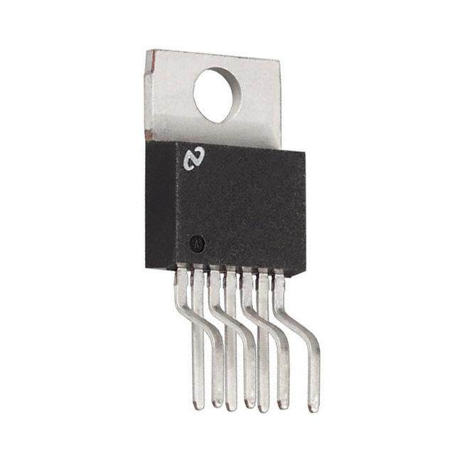
TPS54110 www.ti.com SLVS500D–DECEMBER2003–REVISEDJUNE2019 5 Device Information PACKAGEDDEVICES TJ OUTPUTVOLTAGE PLASTICHTSSOP(PWP)(1) –40°Cto125°C Adjustableto0.891V TPS54110PWP (1) ThePWPpackageisalsoavailabletapedandreeled.AddanRsuffixtothedevicetype(i.e.,TPS54110PWPR).Seeapplication sectionofdatasheetforPowerPADdrawingandlayoutinformation. 6 Pin Configuration and Functions PWPPackage 20-PinHTSSOPWithPowerPAD TopView AGND 1 20 RT VSENSE 2 19 SYNC COMP 3 18 SS/ENA PWRGD 4 17 VBIAS BOOT 5 16 VIN PH 6 15 VIN PH 7 14 VIN PH 8 13 PGND PH 9 12 PGND PH 10 11 PGND PinFunctions PIN DESCRIPTION NAME NO. AGND 1 Analogground—internallyconnectedtothesensitiveanalog-groundcircuitry.ConnecttoPGNDandPowerPAD. Bootstrapinput.0.022-µFto0.1-µFlow-ESRcapacitorconnectedfromBOOTtoPHgeneratesfloatingdriveforthe BOOT 5 high-sideFETdriver. COMP 3 Erroramplifieroutput.ConnectcompensationnetworkfromCOMPtoVSENSE. Powerground.Highcurrentreturnforthelow-sidedriverandpowerMOSFET.ConnectPGNDwithlargecopper PGND 11–13 areastotheinputandoutputsupplyreturns,andnegativeterminalsoftheinputandoutputcapacitors.Connectto AGNDandPowerPAD. PH 6–10 Phaseinput/output.Junctionoftheinternalhighandlow-sidepowerMOSFETs,andoutputinductor. Power-goodopendrainoutput.HighwhenVSENSE≥93%Vref,otherwisePWRGDislow.Notethatoutputislow PWRGD 4 whenSS/ENAisloworinternalshutdownsignalactive. RT 20 Frequencysettingresistorinput.ConnectaresistorfromRTtoAGNDtosettheswitchingfrequency,f . s Slow-start/enableinput/output.Dual-functionpinthatprovideslogicinputtoenable/disabledeviceoperationand SS/ENA 18 capacitorinputtoexternallysetthestart-uptime. Synchronizationinput.Dual-functionpinthatprovideslogicinputtosynchronizetoanexternaloscillatororpinselect SYNC 19 betweentwointernallysetswitchingfrequencies.Whenusedtosynchronizetoanexternalsignal,aresistormustbe connectedtotheRTpin. Internalbiasregulatoroutput.Suppliesregulatedvoltagetointernalcircuitry.BypassVBIASpintoAGNDpinwitha VBIAS 17 highquality,lowESR0.1-µFto1-µFceramiccapacitor. InputsupplyforthepowerMOSFETswitchesandinternalbiasregulator.BypassVINpinstoPGNDpinscloseto VIN 14–16 devicepackagewithahighquality,lowESR1-µFto10-µFceramiccapacitor. VSENSE 2 Erroramplifierinvertinginput. Copyright©2003–2019,TexasInstrumentsIncorporated SubmitDocumentationFeedback 3 ProductFolderLinks:TPS54110
TPS54110 SLVS500D–DECEMBER2003–REVISEDJUNE2019 www.ti.com 7 Specifications 7.1 Absolute Maximum Ratings overoperatingfree-airtemperaturerangeunlessotherwisenoted(1) VALUE UNIT VIN,SS/ENA,SYNC –0.3to7 V RT –0.3to6 V Inputvoltagerange,V I VSENSE –0.3to4 V BOOT –0.3to17 V VBIAS,PWRGD,COMP –0.3to7 V Outputvoltagerange,V O PH –0.6to10 V PH InternallyLimited Sourcecurrent,I O COMP,VBIAS 6 mA PH 3.5 A Sinkcurrent COMP 6 mA SS/ENA,PWRGD 10 mA Voltagedifferential AGNDtoPGND ±0.3 V Continuouspowerdissipation SeeThermalInformation Operatingvirtualjunctiontemperaturerange,T –40to150 °C J Storagetemperature,T –65to150 °C stg (1) Stressesbeyondthoselistedunder“absolutemaximumratings”maycausepermanentdamagetothedevice.Thesearestressratings only,andfunctionaloperationofthedeviceattheseoranyotherconditionsbeyondthoseindicatedunder“recommendedoperating conditions”isnotimplied.Exposuretoabsolute-maximum-ratedconditionsforextendedperiodsmayaffectdevicereliability. 7.2 Recommended Operating Conditions MIN NOM MAX UNIT Inputvoltagerange,V 3 6 V I Operatingjunctiontemperature,T –40 125 °C J 7.3 Thermal Information TPS54110 THERMALMETRIC(1) PWP(HTTSOP) UNIT 20PINS R Junction-to-ambientthermalresistance 34.0 °C/W θJA R Junction-to-case(top)thermalresistance 21.2 °C/W θJC(top) R Junction-to-boardthermalresistance 6.7 °C/W θJB ψ Junction-to-topcharacterizationparameter 0.3 °C/W JT ψ Junction-to-boardcharacterizationparameter 6.5 °C/W JB R Junction-to-case(bottom)thermalresistance 1.5 °C/W θJC(bot) (1) Formoreinformationabouttraditionalandnewthermalmetrics,seetheSemiconductorandICpackagethermalmetricsapplication report. 4 SubmitDocumentationFeedback Copyright©2003–2019,TexasInstrumentsIncorporated ProductFolderLinks:TPS54110
TPS54110 www.ti.com SLVS500D–DECEMBER2003–REVISEDJUNE2019 7.4 Electrical Characteristics T =–40°Cto+125°C,V =3Vto6V(unlessotherwisenoted) J IN PARAMETER TESTCONDITIONS MIN TYP MAX UNIT SUPPLYVOLTAGE,VIN VINinputvoltagerange 3 6 V f =350kHz,SYNC≤0.8V,RTopen 4.5 8.5 s f =550kHz,Phasepinopen, Quiescentcurrent s 5.8 9.6 mA SYNC≥2.5V,RTopen, Shutdown,SS/ENA=0V 1 1.4 UNDERVOLTAGELOCKOUT Startthresholdvoltage,UVLO 2.95 3 V Stopthresholdvoltage,UVLO 2.70 2.80 Hysteresisvoltage,UVLO 0.12 V Risingandfallingedgedeglitch, UVLO(1) 2.5 µs BIASVOLTAGE Outputvoltage,VBIAS I =0 2.70 2.80 2.90 V (VBIAS) V O Outputcurrent,VBIAS(2) 100 µA CUMULATIVEREFERENCE V Accuracy 0.882 0.891 0.900 V ref REGULATION I =0.75A, f =350kHz, T =85°C 0.05 Lineregulation(1)(3) L s J %/V I =0.75A, f =550kHz, T =85°C 0.05 L s J I =0Ato1.5A, f =350kHz, T =85°C 0.01 Loadregulation(1)(3) L s J %/A I =0Ato1.5A f =550kHz, T =85°C 0.01 L s J OSCILLATOR Internallysetfree-running SYNC≤0.8V, RTopen 280 350 420 kHz frequencyrange SYNC≥2.5V, RTopen 440 550 660 RT=180kΩ(1%resistortoAGND)(1) 252 280 308 Externallysetfree-running RT=100kΩ(1%resistortoAGND) 460 500 540 kHz frequencyrange RT=68kΩ(1%resistortoAGND)(1) 663 700 762 High-levelthresholdvoltage, 2.5 V SYNC Low-levelthresholdvoltage, 0.8 V SYNC Pulseduration,SYNC(1) 50 ns Frequencyrange,SYNC(1) 330 700 kHz Rampvalley(1) 0.75 V Rampamplitude(peak-to-peak)(1) 1 V Minimumcontrollableontime(1) 200 ns Maximumdutycycle 90 % (1) Specifiedbydesign (2) Staticresistiveloadsonly (3) SpecifiedbythecircuitusedinFigure9. Copyright©2003–2019,TexasInstrumentsIncorporated SubmitDocumentationFeedback 5 ProductFolderLinks:TPS54110
TPS54110 SLVS500D–DECEMBER2003–REVISEDJUNE2019 www.ti.com Electrical Characteristics (continued) T =–40°Cto+125°C,V =3Vto6V(unlessotherwisenoted) J IN PARAMETER TESTCONDITIONS MIN TYP MAX UNIT ERRORAMPLIFIER Error-amplifieropenloopvoltage 1kΩCOMPtoAGND(1) 90 110 dB gain Error-amplifierunitygain Parallel10kΩ,160pFCOMPtoAGND(1) 3 5 MHz bandwidth Error-amplifiercommon-mode PoweredbyinternalLDO(1) 0 VBIAS V inputvoltagerange I Inputbiascurrent,VSENSE VSENSE=V 60 250 nA IB ref Outputvoltageslewrate VO (symmetric),COMP(1) 1.2 V/µs PWMCOMPARATOR PWMcomparatorpropagation delaytime,PWMcomparator 10mVoverdrive(1) 70 85 ns inputtoPHpin(excludingdead time) SLOW-START/ENABLE Enablethresholdvoltage, 0.82 1.20 1.40 V SS/ENA Enablehysteresisvoltage, SS/ENA(1) 0.03 V Falling-edgedeglitch,SS/ENA(1) 2.5 µs Internalslow-starttime 2.6 3.35 4.1 ms Chargecurrent,SS/ENA SS/ENA=0V 3 5 8 µA Dischargecurrent,SS/ENA SS/ENA=1.3V, V =1.5V 1.5 2.3 4 mA I POWERGOOD Power-goodthresholdvoltage VSENSEfalling 93 %V ref Power-goodhysteresisvoltage(1) 3 %V ref Power-goodfalling-edge deglitch(1) 35 µs Outputsaturationvoltage, I =2.5mA 0.18 0.30 V PWRGD (sink) Leakagecurrent,PWRGD V =5.5V 1 µA I CURRENTLIMIT V =3V,outputshorted(1) 3.0 I Currentlimittrippoint A V =6V,outputshorted(1) 3.5 I Current-limitleadingedge 100 ns blankingtime Current-limittotalresponsetime 200 ns THERMALSHUTDOWN Thermal-shutdowntrippoint(1) 135 150 165 °C Thermal-shutdownhysteresis(1) 10 °C OUTPUTPOWERMOSFETS I =1.5A, V =6V(5) 240 480 r PowerMOSFETswitches(4) O I mΩ DS(on) I =1.5A, V =3V(5) 345 690 O I (4) Includespackageandbondwireresistance (5) MatchedMOSFETs,lowsider productiontested,highsider specifiedbydesign DS(on) DS(on) 6 SubmitDocumentationFeedback Copyright©2003–2019,TexasInstrumentsIncorporated ProductFolderLinks:TPS54110
TPS54110 www.ti.com SLVS500D–DECEMBER2003–REVISEDJUNE2019 7.5 Typical Characteristics 0.6 0.4 Ω VI=3.3V Ω VI=5V −e 0.5 IO=1.5A −e IO=1.5A c c an an 0.3 sist 0.4 sist e e R R e e at 0.3 at 0.2 St St n- n- O O e 0.2 e c c ur ur 0.1 o o S S n- 0.1 n- ai ai Dr Dr 0−40 0 25 85 125 0−40 0 25 85 125 TJ−JunctionTemperature−°C TJ−JunctionTemperature−°C Figure1.Drain-SourceOn-StateResistancevsJunction Figure2.Drain-SourceOn-StateResistancevsJunction Temperature Temperature −kHz 750 −kHz 800 RT=68k Oscillator Frequency 456555000 SYNC≥2.5V Oscillator Frequency 657000000 RT=100k Internally Set 350 SYNC≤0.8V Externally Set 430000 RT= 180 k − 250 − 200 f −40 0 25 85 125 f −40 0 25 85 125 TJ−JunctionTemperature−°C TJ−JunctionTemperature−°C Figure3.InternallySetOscillatorfrequencyvsJunction Figure4.ExternallySetOscillatorfrequencyvsJunction Temperature Temperature 0.895 0.8950 TA=85°C V V 0.893 −n 0.8930 − o Reference 0.891 ge Regulati 0.8910 Voltage 0.889 oltaut V 0.8890 fS=350kHz V−ref0.887 −Outp 0.8870 O V 0.885 0.8850 −40 0 25 85 125 3 4 5 6 TJ−JunctionTemperature−°C VI−InputVoltage−V Figure5.VoltageReferencevsJunctionTemperature Figure6.OutputVoltageRegulationvsInputVoltage Copyright©2003–2019,TexasInstrumentsIncorporated SubmitDocumentationFeedback 7 ProductFolderLinks:TPS54110
TPS54110 SLVS500D–DECEMBER2003–REVISEDJUNE2019 www.ti.com Typical Characteristics (continued) 140 0 3.80 RL=10kΩ, −20 120 CL=160pF, 3.65 TA=25°C −40 ms 100 −60 −e 3.50 s m 80 Phase −80 ee Ti dB egr art 3.35 − 60 −100D St Gain 40 Gain −−112400Phase− nal Slow- 33..2005 20 −160 nter I 2.90 0 −180 −20 −200 2.75 0 10 100 1k 10k 100k 1M 10M −40 0 25 85 125 f−Frequency−Hz TJ−JunctionTemperature−°C Figure7.ErrorAmplifieropenLoopResponse Figure8.InternalSlow-StartTimevsJunctionTemperature 8 SubmitDocumentationFeedback Copyright©2003–2019,TexasInstrumentsIncorporated ProductFolderLinks:TPS54110
TPS54110 www.ti.com SLVS500D–DECEMBER2003–REVISEDJUNE2019 8 Detailed Description 8.1 Overview The TPS54110 low-input-voltage high-output-current synchronous-buck PWM converter integrates all required active components. Included on the substrate with the listed features are a true, high- performance, voltage error amplifier that provides high performance under transient conditions; an undervoltage-lockout circuit to prevent start-up until the input voltage reaches 3 V; an internally and externally set slow-start circuit to limit in-rush currents. 8.2 Functional Block Diagram AGND VBIAS VIN Enable Comparator SS/ENA VBIAS REG Falling SHUTDOWN 1.2 V Edge ILIM VIN Deglitch Thermal Comparator 3 - 6 V Hysteresis: 0.03 V 2.5µs Shutdown Leading 150C° Edge VIN UVLO Blanking Comparator Falling 100 ns and VIN Rising BOOT 2.95 V Edge Hysteresis: 0.16 V Deglitch 2.5µs SS_DIS SHUTDOWN PH LOUT VO Internal/External Slow-start + (Internal Slow-startTime = 3.35 ms - RQ Adaptive Dead-Time CO and Error S Control Logic Amplifier PWM Reference Comparator VIN VREF = 0.891 V OSC PGND Powergood Comparator PWRGD VSENSE Falling 0.93 Vref Edge TPS54110 Deglitch Hysteresis: 0.03 Vref SHUTDOWN 35µs VSENSE COMP RT SYNC Copyright©2003–2019,TexasInstrumentsIncorporated SubmitDocumentationFeedback 9 ProductFolderLinks:TPS54110
TPS54110 SLVS500D–DECEMBER2003–REVISEDJUNE2019 www.ti.com 8.3 Feature Description 8.3.1 VBIASRegulator(VBIAS) The VBIAS regulator provides internal analog and digital blocks with a stable supply voltage over variations in junction temperature and input voltage. A high quality, low-ESR, ceramic bypass capacitor is required on the VBIAS pin. X7R or X5R grade dielectrics are recommended because their values are more stable over temperature. Place the bypass capacitor close to the VBIAS pin and returned to AGND. External loading on VBIAS is allowed, with the caution that internal circuits require a minimum VBIAS of 2.7 V, and external loads on VBIAS with ac or digital switching noise may degrade performance. The VBIAS pin may be useful as a reference voltageforexternalcircuits. 8.3.2 VoltageReference The voltage reference system produces a precise V signal by scaling the output of a temperature stable ref bandgap circuit. During manufacture, the bandgap and scaling circuits are trimmed to produce 0.891 V at the output of the error amplifier, with the amplifier connected as a voltage follower. The trim procedure adds to the high precision regulation of the TPS54110 because it cancels offset errors in the scale and error amplifier circuits. 8.3.3 OscillatorandPWMRamp The oscillator frequency can be set to internally fixed values of 350 kHz or 550 kHz using the SYNC pin as a static digital input. If a different frequency of operation is required for the application, the oscillator frequency can be externally adjusted from 280 kHz to 700 kHz by connecting a resistor from the RT pin to ground and floating the SYNC pin. The switching frequency is approximated by the following equation, where R is the resistance fromRTtoAGND: 100kW SWITCHINGFREQUENCY= ´500kHz R (1) ExternalsynchronizationofthePWMrampispossibleoverthefrequencyrangeof330kHzto700kHzby driving asynchronizationsignalinto SYNC and connecting a resistor from RT to AGND. Choose an RT resistor that sets the free-running frequency to 80% of the synchronization signal. Table 1 summarizes the frequency selection configurations. Table1.SummaryOfTheFrequencySelectionConfigurations SWITCHINGFREQUENCY SYNCPIN RTPIN 350kHz,internallyset FloatorAGND Float 550kHz,internallyset ≥2.5V Float Externallyset280kHzto700kHz Float R=68kto180k Externallysynchronized R=RTvaluefor80%ofexternal Synchronizationsignal frequency synchronizationfrequency 8.3.4 ErrorAmplifier The high-performance, wide-bandwidth, voltage error amplifier sets the TPS54110 apart from most dc/dc converters. The user is given the flexibility to use a wide range of output L- and C-filter components to suit the particular application needs. Type-2 or type-3 compensation can be employed using external compensation components. 8.3.5 PWMControl Signals from the error-amplifier output, oscillator, and current-limit circuit are processed by the PWM control logic. Referring to the internal block diagram, the control logic includes the PWM comparator, OR gate, PWM latch, and portions of the adaptive dead-time and control-logic block. During steady-state operation below the current-limit threshold, the PWM-comparator output and oscillator pulse train alternately reset and set the PWM latch. Once the PWM latch is set, the low-side FET remains on for a minimum duration set by the oscillator pulse 10 SubmitDocumentationFeedback Copyright©2003–2019,TexasInstrumentsIncorporated ProductFolderLinks:TPS54110
TPS54110 www.ti.com SLVS500D–DECEMBER2003–REVISEDJUNE2019 duration. During this period, the PWM ramp discharges rapidly to its valley voltage. When the ramp begins to charge back up, the low-side FET turns off and high-side FET turns on. As the PWM ramp voltage exceeds the error-amplifier output voltage, the PWM comparator resets the latch, thus turning off the high-side FET and turning on the low-side FET. The low-side FET remains on until the next oscillator pulse discharges the PWM ramp. During transient conditions, the error amplifier output could be below the PWM ramp valley voltage or above the PWM peak voltage. If the error-amplifier output is high, the PWM latch is never reset and the high-side FET remains on until the oscillator pulse signals the control logic to turn the high-side FET off and the low-side FET on. The device operates at its maximum duty cycle until the output voltage rises to the regulation set-point, setting VSENSE to approximately the same voltage as V . If the error-amplifier output is low, the PWM latch is ref continually reset and the high-side FET does not turn on. The low-side FET remains on until the VSENSE voltage decreases to a range that allows the PWM comparator to change states. The TPS54110 is capable of sinkingcurrentcontinuouslyuntiltheoutputreachestheregulationset-point. If the current-limit comparator remains tripped longer than 100 ns, the PWM latch resets before the PWM ramp exceeds the error-amplifier output. The high-side FET turns off and low-side FET turns on to decrease the energy in the output inductor, and consequently the output current. This process is repeated each cycle that the current-limitcomparatoristripped. 8.3.6 Dead-TimeControlandMOSFETDrivers Adaptive dead-time control prevents shoot-through current from flowing in both N-channel power MOSFETs during the switching transitions by actively controlling the turn-on times of the MOSFET drivers. The high-side driver does not turn on until the gate-drive voltage to the low-side FET is below 2 V. The low-side driver does not turn on until the voltage at the gate of the high-side MOSFETs is below 2 V. The high-side and low-side drivers are designed with 300-mA source and sink capability to quickly drive the power MOSFETs gates. The low-side driver is supplied from VIN, while the high-side driver is supplied from the BOOT pin. A bootstrap circuit uses an external BOOT capacitor and an internal 2.5-Ω bootstrap switch connected between the VIN and BOOT pins. Theintegratedbootstrapswitchimprovesdriveefficiencyandreducesexternal-componentcount. 8.3.7 OvercurrentProtection Cycle-by-cycle current limiting is achieved by sensing the current flowing through the high-side MOSFET and differential amplifier and comparing it to the preset overcurrent threshold. The high-side MOSFET is turned off within 200 ns of reaching the current-limit threshold. A 100-ns leading-edge blanking circuit prevents false tripping of the current limit. Current-limit detection occurs only when current flows from VIN to PH when sourcing currenttotheoutputfilter.Loadprotectionduringcurrent-sinkoperationisprovidedbythermalshutdown. 8.3.8 ThermalShutdown The device uses the thermal shutdown to turn off the power MOSFETs and disable the controller if the junction temperature exceeds 150°C. The device is released from shutdown when the junction temperature decreases to 10°C below the thermal-shutdown trip point, and starts up under control of the slow-start circuit. Thermal shutdown provides protection when an overload condition is sustained for several milliseconds. In a persistent- fault condition, the device cycles continuously; starting up under control of the soft-start circuit, heating up due to thefault,andthenshuttingdownuponreachingthethermal-shutdownpoint. 8.3.9 PowerGood(PWRDG) Thepower-goodcircuitmonitors for undervoltage conditions on VSENSE. If the voltage on VSENSE is 7% below the reference voltage, the open-drain PWRGD output is pulled low. PWRGD is also pulled low if V is less than IN the UVLO threshold, or SS/ENA is low, or if thermal shutdown asserts. When VIN = UVLO threshold, SS/ENA = enable threshold, and VSENSE > 93% of V , the open-drain output of the PWRGD pin is high. A hysteresis ref voltage equal to 3% of V and a 35-µs falling-edge deglitch circuit prevent tripping of the power-good ref comparatorduetohighfrequencynoise. Copyright©2003–2019,TexasInstrumentsIncorporated SubmitDocumentationFeedback 11 ProductFolderLinks:TPS54110
TPS54110 SLVS500D–DECEMBER2003–REVISEDJUNE2019 www.ti.com 8.4 Undervoltage Lockout (UVLO) The TPS54110 incorporates an under voltage lockout circuit to keep the device disabled when the input voltage (VIN) is insufficient. During power up, internal circuits are held inactive until V exceeds the nominal UVLO IN threshold voltage of 2.95 V. Once the UVLO start threshold is reached, device start-up begins. The device operates until VIN falls below the nominal UVLO stop threshold of 2.8 V. Hysteresis in the UVLO comparator, and a 2.5-µs rising and falling edge deglitch circuit reduce the likelihood of shutting the device down due to noise onVIN. 8.5 Slow-Start/Enable (SS/ENA) The slow-start/enable pin provides two functions; first, the pin acts as an enable (shutdown) control by keeping the device turned off until the voltage exceeds the start threshold voltage of approximately 1.2 V. When SS/ENA exceeds the enable threshold, device start up begins. The reference voltage fed to the error amplifier is linearly ramped up from 0 V to 0.891 V in 3.35 ms. Similarly, the converter output voltage reaches regulation in approximately 3.35 ms. Voltage hysteresis and a 2.5-µs falling edge deglitch circuit reduce the likelihood of triggeringtheenableduetonoise. The second function of the SS/ENA pin provides an external means of extending the slow-start time with a low- value capacitor connected between SS/ENA and AGND. Adding a capacitor to the SS/ENA pin has two effects on start-up. First, a delay occurs between release of the SS/ENA pin and start up of the output. The delay is proportional to the slow-start capacitor value and lasts until the SS/ENA pin reaches the enable threshold. The start-updelayisapproximately: 1.2V t =C ´ d (SS) 5ma (2) Second,astheoutputbecomesactive,abrieframp-upat the internal slow-start rate may be observed before the externally set slow-start rate takes control and the output rises at a rate proportional to the slow-start capacitor. Theslow-starttimesetbythecapacitorisapproximately: 0.7V t =C ´ (SS) (SS) 5ma (3) The actual slow-start is likely to be less than the above approximation due to the brief ramp-up at the internal rate. 12 SubmitDocumentationFeedback Copyright©2003–2019,TexasInstrumentsIncorporated ProductFolderLinks:TPS54110
TPS54110 www.ti.com SLVS500D–DECEMBER2003–REVISEDJUNE2019 9 Application and Implementation NOTE Information in the following applications sections is not part of the TI component specification, and TI does not warrant its accuracy or completeness. TI’s customers are responsible for determining suitability of components for their purposes. Customers should validateandtesttheirdesignimplementationtoconfirmsystemfunctionality. 9.1 Application Information The TPS54110 low-input-voltage high-output-current synchronous-buck PWM converter integrates all required active components. Included on the substrate with the listed features are a true, high- performance, voltage error amplifier that provides high performance under transient conditions; an undervoltage-lockout circuit to prevent start-up until the input voltage reaches 3 V; an internally and externally set slow-start circuit to limit in-rush currents;andapower-goodoutputusefulforprocessor/logicreset,faultsignaling,andsupplysequencing. 9.2 Typical Applications 9.2.1 TypicalTPS54110Application Figure 9 shows the schematic diagram for a typical TPS54110 application. The TPS54110 can provide up to 1.5 A of output current at a nominal output voltage of 3.3 V. For proper thermal performance, the exposed PowerPADunderneaththedevicemustbesoldereddowntotheprinted-circuitboard. R7 VIN(4.5−5.5 V) 10 kΩ PWRGD C8 R5 2200 pF 2.05 kΩ + R4 U2 C1 71.5 kΩ TPS54110PWP R3 C6 10µF 20 RT AGND 1 19.1 kΩ 2700 pF 19 SYNC VSENSE 2 R1 18 3 C7 10.7 kΩ 17 SS/ENA COMP 4 33 pF R3.292 kΩ VBIAS PWRGD 16 5 C3 0.047µF VIN BOOT 15 6 VIN PH 14 7 VIN PH C5 C4 C9 13 8 .047 µF 0.1 µF 10 µF PGND PH L1 12 9 6.8µH PGND PH 11 10 1 2 PGND PH PwrPd 3.3 V at 1.5A 21 C2 100 µF Figure9. ApplicationSchematic Copyright©2003–2019,TexasInstrumentsIncorporated SubmitDocumentationFeedback 13 ProductFolderLinks:TPS54110
TPS54110 SLVS500D–DECEMBER2003–REVISEDJUNE2019 www.ti.com Typical Applications (continued) 9.2.1.1 DesignRequirements Therequiredparameterstobeginthedesignprocessandvaluesforthisdesign example are listed in Table 2. As anadditionalconstraint,thedesignissetuptobesmallsizeandlowcomponentheight. Table2.DesignParameters DESIGNPARAMETER EXAMPLEVALUE Inputvoltagerange 4.5to5.5V Outputvoltage 3.3V Inputripplevoltage 100mV Outputripplevoltage 30mV Outputcurrentrating 1.5A Operatingfrequency 700kHz 9.2.1.2 DetailedDesignProcedure 9.2.1.2.1 SwitchingFrequency The switching frequency is set within the range of 280 kHz to 700 kHz by connecting a resistor from the RT pin toAGND.Equation4 isusedtodeterminetheproperRTvalue. 100´500kHz RT(kW) = ¦ s(kHz) (4) Inthisexample,thetiming-resistorvaluechosenforR4is71.5kΩ,settingtheswitchingfrequencyto700kHz. Alternately, the TPS54110 can be set to preprogrammed switching frequencies of 350 kHz or 550 kHz by connectingpinsRTandSYNCasshowninTable3. Table3.DesignParameters FREQUENCY RT SYNC 350kHz Float FloatorAGND 550kHz Float ≥2.5V 9.2.1.2.2 InputCapacitors The TPS54110 requires an input decoupling capacitor and, depending on the application, a bulk input capacitor. The minimum value for the decoupling capacitor, C9, is 10 uF. A high quality ceramic type X5R or X7R with a voltage rating greater than the maximum input voltage is recommended. A bulk input capacitor may be needed, especially if the TPS54110 circuit is not located within approximately 2 inches from the input voltage source. The capacitance value is not critical, but the voltage rating must be greater than the maximum input voltage including ripplevoltage.Thecapacitormustfiltertheinputripplevoltagetoacceptablelevels. InputripplevoltagecanbeapproximatedbyEquation5: I DV OUT(MAX)´0.25+(I ESR ) IN= C ¦ OUT(MAX)´ MAX BULK´ SW where • I isthemaximumloadcurrent OUT(MAX) • ƒ istheswitchingfrequency SW • C isthebulkcapacitorvalue BULK • ESR isthemaximumseriesresistanceofthebulkcapacitor (5) MAX Worst-caseRMSripplecurrentisapproximatedbyEquation6: I I = OUT(MAX) CIN 2 (6) 14 SubmitDocumentationFeedback Copyright©2003–2019,TexasInstrumentsIncorporated ProductFolderLinks:TPS54110
TPS54110 www.ti.com SLVS500D–DECEMBER2003–REVISEDJUNE2019 In this case the input ripple voltage is 66 mV with a 10-µF bulk capacitor. Figure 14 shows the measured ripple waveform. The RMS ripple current is 0.75 A. The maximum voltage across the input capacitors is V + INMAX ΔV /2. The bypass capacitor and input bulk capacitor are each rated for 6.3 V and a ripple-current capacity of IN 1.5 A, providing some margin. It is very important that the maximum ratings for voltage and current are not exceededunderanycircumstance. 9.2.1.2.3 OutputFilterComponents Two components, L1 and C2, are selected for the output filter. Since the TPS54110 is an externally- compensateddevice,awiderangeoffilter-componenttypesandvaluesaresupported. 9.2.1.2.3.1 InductorSelection UseEquation7tocalculatetheminimumvalueoftheoutputinductor: V ´(V -V ) L = OUT IN(MAX) OUT MIN V ´K ´I ´F IN(MAX) IND OUT SW (7) K is a coefficient that represents the amount of inductor ripple current relative to the maximum output current. IND For designs using low-ESR capacitors such as ceramics, use K = 0.2. When using higher ESR output IND capacitors, K = 0.1 yields better results. If higher ripple currents can be tolerated, K can be increased IND IND allowingforasmalleroutput-inductorvalue. This example design uses K = 0.2, yielding a minimum inductor value of 6.29 µH. The next-higher standard IND value of 6.8 µH is chosen for this design. If a lower inductor value is desired, a larger amount of ripple current mustbetolerated. The RMS-current and saturation-current ratings of the output filter inductor must not be exceeded. The RMS inductorcurrentcanbefoundfromEquation8: 1 æ V ´(V -V ) ö2 IL(RMS)= I2OUT(MAX)+12´çèVINO(MUTAX)´LIONU(MTA´XF) SW´OU0T.8÷ø (8) ThepeakinductorcurrentisdeterminedfromEquation9: V ´(V -V ) I =I + OUT IN(MAX) OUT L(PK) OUT(MAX) 1.6´V ´L ´F IN(MAX) OUT SW (9) For this design, the RMS inductor current is 1.503 A and the peak inductor current is 1.673 A. The inductor chosen is a Coilcraft DS3316P-682 6.8 µH. It has a saturation current rating of 2.8 A and an RMS current rating of2.2A,easilymeetingtheserequirements. 9.2.1.2.3.2 CapacitorSelection The important design parameters for the output capacitor are dc voltage, ripple current, and equivalent series resistance (ESR). The dc-voltage and ripple-current ratings must not be exceeded. The ESR rating is important because along with the inductor current it determines the output ripple voltage level. The actual value of the output capacitor is not critical, but some practical limits do exist. Consider the relationship between the desired closed-loop crossover frequency of the design and LC corner frequency of the output filter. In general, it is desirable to keep the closed-loop crossover frequency at less than 1/5 of the switching frequency. With high switching frequencies such as the 700 kHz frequency of this design, internal circuit limitations of the TPS54110 limit the practical maximum crossover frequency to about 100 kHz. To allow adequate phase gain in the compensation network, set the LC corner frequency to approximately one decade below the closed-loop crossoverfrequency.Thislimitstheminimumcapacitorvaluefortheoutputfilterto: 1 æ K ö2 COUT(MIN)=LOUT´çè2p¦CO÷ø where • Kisthefrequencymultiplierforthespreadbetweenf LC • f .Kshouldbebetween5and15,typically10foronedecadeofdifference. (10) CO Copyright©2003–2019,TexasInstrumentsIncorporated SubmitDocumentationFeedback 15 ProductFolderLinks:TPS54110
TPS54110 SLVS500D–DECEMBER2003–REVISEDJUNE2019 www.ti.com For a desired crossover of 60 kHz, K=10 and a 6.8 μH inductor, the minimum value for the output capacitor is 100 μF. The selected output capacitor must be rated for a voltage greater than the desired output voltage plus one half the ripple voltage. Any derating factors must also be included. The maximum RMS ripple current in the outputcapacitorisgivenbyEquation11: 1 é V ´(V -V ) ù ICOUT(RMS)= 12´êëV OUT ´LIN(MA´X)F O´UNT úû IN(MAX) OUT SW C where • NCisthenumberofoutputcapacitorsinparallel (11) The maximum ESR of the output capacitor is determined by the allowable output ripple specified in the initial design parameters. The output ripple voltage is the inductor ripple current times the ESR of the output filter so themaximumspecifiedESRaslistedinthecapacitordatasheetisgivenbyEquation12: æV ´L ´F ´0.8ö ESR =N ´ç IN(MAX) OUT SW ÷´DV MAX C ç V ´(V -V ) ÷ p-p(MAX) è OUT IN(MAX) OUT ø (12) For this design example, a single 100-µF output capacitor is chosen for C2. The calculated RMS ripple current is 80 mA and the maximum ESR required is 87 mΩ. An example of a suitable capacitor is the Sanyo Poscap 6TPC100M,ratedat6.3VwithamaximumESRof45mΩ andaripple-currentratingof1.7A. OthercapacitortypesworkwellwiththeTPS54110,dependingontheneedsoftheapplication. 9.2.1.2.4 CompensationComponents The external compensation used with the TPS54110 allows for a wide range of output-filter configurations. A large range of capacitor values and dielectric types are supported. The design example uses type 3 compensation consisting of R1, R3, R5, C6, C7 and C8. Additionally, R2 and R1 form a voltage-divider network that sets the output voltage. These component reference designators are the same as those used in the SWIFT DesignerSoftware. There are a number of different ways to design a compensation network. This procedure outlines a relatively simple procedure that produces good results with most output filter combinations. Use the SWIFT Designer Software for designs with unusually high closed-loop crossover frequencies; with low-value, low-ESR output capacitorssuchasceramics;orifyouareunsureaboutthedesignprocedure. A number of considerations apply when designing compensation networks for the TPS54110. The compensated error-amplifier gain must not be limited by the open-loop amplifier gain characteristics and must not produce excessive gain at the switching frequency. Also, the closed-loop crossover frequency must be set less than one fifth of the switching frequency, and the phase margin at crossover must be greater than 45 degrees. The general procedure outlined here meets these requirements without going into great detail about the theory of loopcompensation. First,calculatetheoutputfilterLCcornerfrequencyusingEquation13: 1 ¦ = LC 2p LOUTCOUT (13) Forthedesignexample,ƒ =6103Hz. LC Choose a closed-loop crossover frequency greater than f and less than one fifth of the switching frequency. LC Also, keep the crossover frequency below 100 kHz, as the error amplifier may not provide the desired gain at higher frequencies. The 60-kHz crossover frequency chosen for this design provides comparatively wide loop bandwidthwhilestillallowingadequatephaseboosttoensurestability. 16 SubmitDocumentationFeedback Copyright©2003–2019,TexasInstrumentsIncorporated ProductFolderLinks:TPS54110
TPS54110 www.ti.com SLVS500D–DECEMBER2003–REVISEDJUNE2019 Next,the values for the compensation components that set the poles and zeros of the compensation network are calculated. Assuming an R1 value > than R5 and a C6 value > C7, the pole and zero locations are given by Equation14throughEquation17: 1 ¦ = Z1 2pR3C6 (14) 1 ¦ = Z2 2pR1C8 (15) 1 ¦ = P1 2pR5C8 (16) 1 ¦ = P2 2pR3C7 (17) Additionallythereisapoleattheorigin,whichhasunitygainatafrequency: 1 ¦ = INT 2pR1C6 (18) This pole is used to set the overall gain of the compensated error amplifier and determines the closed loop crossover frequency. Since R1 is given as 10 kΩ and the crossover frequency is selected as 60 kHz, the desired f iscalculatedfromEquation19: INT 10-0.74 ´ ¦ ¦ = CO INT 2 (19) AndthevalueforC6isgivenbyEquation20: 1 C6= 2pR1¦ INT (20) Since C6 is calculated to be 2900 pF, and the location of the integrator crossover frequency is important in setting the overall loop crossover, adjust the value of R1 so that C6 is a standard value of 2700 pF, using Equation21: 1 R1= 2pC6¦ LC (21) ThevalueforR1is10.7KΩ Thefirstzero,f islocatedatonehalftheoutputfilterLCcornerfrequency,soR3iscalculatedfrom: Z1 1 R3= pC6¦ LC (22) Thesecondzero, f islocatedattheoutputfilterLCcornerfrequency,soC8iscalculatedfrom: Z2 1 C8= 2pR1¦ LC (23) Thefirstpole, f islocatedtocoincidewithoutputfilterESRzerofrequency.Thisfrequencyisgivenby: P1 1 ¦ = ESR0 2pR C ESR OUT where • R istheequivalentseriesresistanceoftheoutputcapacitor (24) ESR Inthiscase,theESRzerofrequencyis35.4kHz,andR5iscalculatedfrom: 1 R5= 2pC8¦ ESR (25) Copyright©2003–2019,TexasInstrumentsIncorporated SubmitDocumentationFeedback 17 ProductFolderLinks:TPS54110
TPS54110 SLVS500D–DECEMBER2003–REVISEDJUNE2019 www.ti.com The final pole is placed at a frequency high enough above the closed-loop crossover frequency to avoid causing an excessive phase decrease at the crossover frequency while still providing enough attenuation so that there is little or no gain at the switching frequency. The f pole location for this circuit is set to 4 times the closed-loop P2 crossoverfrequencyandthelastcompensationcomponentvalueC7isderived: 1 C7= 8pR3¦ CO (26) Finally,calculatetheR2resistorvaluefortheoutputvoltageof3.3VusingEquation27: R1 ´ 0.891 R2= V -0.891 OUT (27) ForthisTPS54110design,useR1=10.7kΩinsteadof10.0kΩ.R2isthen3.92kΩ. Since capacitors are only available in a limited range of standard values, the nearest standard value was chosen foreachcapacitor.Themeasuredclosed-loopresponseforthisdesignisshowninFigure18. 9.2.1.2.5 BiasandBootstrapCapacitors Every TPS54110 design requires a bootstrap capacitor (C3), and a bias capacitor (C4). The bootstrap capacitor must be between 0.022 µF and 0.1 µF. This design uses 0.047 µF. The bootstrap capacitor is located between the PH pins and BOOT. The bias capacitor is connected between the VBIAS pin and AGND. Recommended values are 0.1 µF to 1 µF. This design uses 0.1 µF. Use high-quality ceramic capacitors with X7R or X5R grade dielectricfortemperaturestability.Placethemasclosetothedevicepinsaspossible. 18 SubmitDocumentationFeedback Copyright©2003–2019,TexasInstrumentsIncorporated ProductFolderLinks:TPS54110
TPS54110 www.ti.com SLVS500D–DECEMBER2003–REVISEDJUNE2019 9.2.1.3 ApplicationCurves AllperformancedatashownforV =5V,V =3.3V,f =700kHz,T =25°C,Figure9 I O s A 100 1.2 95 90 W 1 − % 8805 pation 0.8 − si Efficiency 7705 Power Dis 00..46 65 − D 60 P 0.2 55 50 0 0 0.25 0.5 0.75 1 1.25 1.5 0 0.25 0.5 0.75 1 1.25 1.5 IO−Output Current−A IO−Output Current−A Figure10.EfficiencyvsOutputCurrent Figure11.PowerDissipationvsOutputCurrent 0.05 0.02 0.04 0.015 % 0.03 % Ou−tputVoltageVaristion−−−00000.....00000123210 Output−VoltageVaristion−−00.00.00..000051015 IO=0A IO=1.5AIO=0.75A −0.04 −0.015 −0.05 −0.02 0 0.25 0.5 0.75 1 1.25 1.5 4.5 4.75 5 5.25 5.5 IO−Output Current−A VI−InputVoltage−V Figure12.LoadRegulationvsOutputCurrent Figure13.LineRegulationvsInputVoltage VI=50mV/div(AC) VO=10mV/div(AC) V(phase)=2V/div V(phase)=2V/div Time=500ns/div Time=500ns/div Figure14.InputVoltageRipple Figure15.OutputVoltageRipple Copyright©2003–2019,TexasInstrumentsIncorporated SubmitDocumentationFeedback 19 ProductFolderLinks:TPS54110
TPS54110 SLVS500D–DECEMBER2003–REVISEDJUNE2019 www.ti.com VI=2V/div VO=10mV/div(AC) IO=1V/div VO=1V/div Time=200 s/div Time=5ms/div Figure16.OutputVoltageTransientResponse Figure17.StartUpWaveform 60 180 50 150 40 Phase 120 30 90 20 60 s e dB 10 Gain 30 egre − 0 0 D n − Gai−10 −30se −20 −60ha P −30 −90 −40 −120 −50 −150 −60 −180 100 1k 10k 100k 1M f−Frequency−Hz Figure18.MeasuredLoopResponse 20 SubmitDocumentationFeedback Copyright©2003–2019,TexasInstrumentsIncorporated ProductFolderLinks:TPS54110
TPS54110 www.ti.com SLVS500D–DECEMBER2003–REVISEDJUNE2019 9.2.2 Very-SmallForm-FactorApplication Figure 19 shows an application schematic for a TPS54110 application designed for extremely small size. To achievethisgoal,thedesignproceduregiven in the previous application circuit is modified. For example, in order to use a small-footprint Coilcraft DO3314-103MX inductor, the maximum-allowable inductor ripple current was increased above that normally specified. A small 0805 10-µF ceramic capacitor is used in the output filter. All the additionalcomponentsare0402casesize. R7 VIN 10 kΩ PWRGD C8 R5 560 pF 432Ω + R4 U2 C1 71.5 kΩ TPS54110PWP R3 C6 OPEN 20 RT AGND 1 1.74 kΩ 1000 pF 19 SYNC VSENSE 2 R1 18 3 C7 10.0 kΩ SS/ENA COMP 47 pF R2 17 4 14.7 kΩ VBIAS PWRGD 16 5 C3 0.047 µF VIN BOOT 15 6 VIN PH 14 7 VIN PH C5 C4 C9 13 8 OPEN 0.1 µF 10 µF PGND PH L1 12 9 1 µH PGND PH 11 10 1 2 PGND PH PwrPd 1.5 V at 1.5A 21 C2 10 µF Figure19. SmallForm-FactorReferenceDesign 9.2.2.1 DesignRequirements SeeDesignRequirements 9.2.2.2 DetailedDesignProcedure SeeDetailedDesignProcedure Copyright©2003–2019,TexasInstrumentsIncorporated SubmitDocumentationFeedback 21 ProductFolderLinks:TPS54110
TPS54110 SLVS500D–DECEMBER2003–REVISEDJUNE2019 www.ti.com 9.2.2.3 ApplicationCurves AllperformancedatashownforV =5V,V =1.5V,F =700kHz,T =25°C,Figure19 I O S A 100 95 W 1.2 90 − n 85 o 1 −% 80 VI=5V sipati 0.8 Efficiency 7705 Power Dis 0.6 VI=5V 65 − 0.4 D P 60 VI=3.3V 0.2 55 VI=3.3V 50 0 0 0.25 0.5 0.75 1 1.25 1.5 0 0.25 0.5 0.75 1 1.25 1.5 IO−Output Current−A IO−Output Current−A Figure20.EfficiencyvsOutputCurrent Figure21.PowerDissipationvsOutputCurrent 0.1 0.02 0.08 0.015 % utput−%VoltageVaristion−−−000000......0000002460642 VI=5V VI=3.3V OutputV−oltageVaristion−−00.00.00..000051015 IO=0A IO=1.5IOA=0.75A O −0.015 −0.08 −0.1 −0.02 0 0.25 0.5 0.75 1 1.25 1.5 3 3.5 4 4.5 5 5.5 6 IO−OutputCurrent−A VI−InputVoltage−V Figure22.LoadRegulationvsOutputCurrent Figure23.LineRegulationvsInputVoltage VI=50mV/div(AC) VO=20mV/div(AC) V(phase)=2V/div V(phase)=2V/div Time=500ns/div Time=500ns/div Figure24.InputVoltageRipple Figure25.OutputVoltageRipple 22 SubmitDocumentationFeedback Copyright©2003–2019,TexasInstrumentsIncorporated ProductFolderLinks:TPS54110
TPS54110 www.ti.com SLVS500D–DECEMBER2003–REVISEDJUNE2019 VO=20mV/div(AC) VI=1V/div VO=500mV/div IO=1V/div Time=200 s/div Time=5ms/div Figure26.OutputVoltageTransientresponse Figure27.StartUpWaveform Copyright©2003–2019,TexasInstrumentsIncorporated SubmitDocumentationFeedback 23 ProductFolderLinks:TPS54110
TPS54110 SLVS500D–DECEMBER2003–REVISEDJUNE2019 www.ti.com 9.2.3 Two-OutputSequenced-StartupApplication InFigure28, the power-good output of U1 is used as a sequencing signal in a two-output design. Connecting the PWRGD pin of U1 to the SS/ENA pin of U2 causes the 1.5-V output to ramp up after the 3.3-V output is within regulation.Figure29showsthestart-upwaveformsassociatedwiththiscircuit. WhenV reachestheUVLO-startthreshold,theU1outputrampsuptowardsthe3.3-Vsetpoint.Aftertheoutput IN reaches 90 percent of 3.3 V, the U1 asserts the power-good signal driving the U2 SS/ENA input high. The output ofU2thenrampsuptowardsthefinaloutputsetpointof1.5V. PWRGD_3P3 VI5V R7 + 10kΩ 56C08pF 43R25Ω U1 C4710µF 71.R54kΩ 20 RTTPS54110APGWNPD 1 1.7R43kΩ100C06pF 1198 SYNC VSENSE 32 C7 10R1kΩ SS/ENA COMP 47pF R2 17 VBIAS PWRGD 4 3.74kΩ 16 5 C3 0.047µF VIN BOOT 15 6 C4 VIN PH 0.1µF 14 VIN PH 7 13 8 PGND PH L1 12 PGND PH 9 1µH 10CµF9 11 PGND PH 10 1 2 VOUT1 PWPD 3.3Vat1.5A 21 C2 10µF R8 PWRGD_1P5 10kΩ 56C013pF 4R3212Ω U2 71.R59kΩ 20 RTTPS54110APGWNPD 1 1.7R46kΩ100C05pF 1198 SYNC VSENSE 32 C11 1R01k1Ω SS/ENA COMP 47pF R10 17 VBIAS PWRGD 4 14.7kΩ 16 5 C14 0.047µF VIN BOOT 15 6 C10 VIN PH 0.1µF 14 VIN PH 7 13 8 PGND PH L2 10Cµ1F5 1112 PPGGNNDD PPHH 190 1 1µH 2 VOUT2 PWPD 1.5Vat1.5A 21 C12 10µF Figure28. TPS54110SequencingApplicationCircuit 9.2.3.1 DesignRequirements SeeDesignRequirements 9.2.3.2 DetailedDesignProcedure SeeDetailedDesignProcedure 24 SubmitDocumentationFeedback Copyright©2003–2019,TexasInstrumentsIncorporated ProductFolderLinks:TPS54110
TPS54110 www.ti.com SLVS500D–DECEMBER2003–REVISEDJUNE2019 9.2.3.3 ApplicationCurve V −5 V/div IN U1−V OUT1 3.3−2 V/div U1 PWRGD −5 V/div U2−V 1.5−2 V/div OUT2 Figure29.SequencingStart-UpWaveforms Copyright©2003–2019,TexasInstrumentsIncorporated SubmitDocumentationFeedback 25 ProductFolderLinks:TPS54110
TPS54110 SLVS500D–DECEMBER2003–REVISEDJUNE2019 www.ti.com 10 Layout 10.1 Layout Guidelines The VIN pins are connected together on the printed board (PCB) and bypassed with a low-ESR ceramic bypass capacitor. Minimize the loop area formed by the bypass capacitor connections, the VIN pins, and the TPS54110 ground pins. The recommended bypass capacitor is 10-μF (minimum) ceramic with X5R or X7R dielectric. The optimum placement is closest to the VIN pins and the AGND and PGND pins. See Figure 30 for an example layout. It has an area of ground on the top layer directly under the IC, with an exposed area for connection to the PowerPAD.Useviastoconnectthisgroundareatoanyinternalgroundplanes.Useadditionalvias at the ground side of the input and output filter capacitors as well. Tie the AGND and PGND pins to the PCB ground area under the device as shown. Use a separate wide trace for the analog-ground path, connecting the voltage set- point divider, timing resistor RT, slow-start capacitor and bias-capacitor grounds. Tie the PH pins together and route to the output inductor. Since the PH connection is the switching node, locate the inductor very close to the PH pins, and minimize the area of the conductor to prevent excessive capacitive coupling. Connect the boot capacitor between the phase node and the BOOT pin as shown. Keep the boot capacitor close to the IC and minimize the conductor trace lengths. Connect the output-filter capacitor(s) as shown between the VOUT trace and PGND. It is important to keep the loop formed by the PH pins, L , C , and PGND as small as is OUT OUT practical. Place the compensation components from the VOUT trace to the VSENSE and COMP pins. Do not place these components too close to the PH trace. Due to the size of the IC package and the device pin-out, they must be somewhat closely routed while maintaining as much separation as possible, yet keeping the layout compact. Connect the bias capacitor from the VBIAS pin to analog ground using the isolated analog ground trace. If a slow-start capacitor or RT resistor is used, or if the SYNC pin is used to select 350-kHz operating frequency,connectthemtothistraceaswell. 10.2 Layout Example ANALOGGROUNDTRACE FREQUENCYSETRESISTOR AGND RT VSENSE SYNC SLOWSTART CAPACITOR COMPENSATION COMP SS/ENA NETWORK PWRGD VBIAS BIASCAPACITOR BOOT Exposed CAPACITOR BOOT Powerpad VIN Area VIN PH VIN VOUT PH VIN LOUT PH PGND OUTPUTINDUCTOR PH PGND PH PH PGND COUT INPUT INPUT BYPASS BULK CAPACITOR FILTER OUTPUT FILTER PGND CAPACITOR TOPSIDE GROUNDAREA VIA to Ground Plane Figure30. PCBoardLayoutExample 26 SubmitDocumentationFeedback Copyright©2003–2019,TexasInstrumentsIncorporated ProductFolderLinks:TPS54110
TPS54110 www.ti.com SLVS500D–DECEMBER2003–REVISEDJUNE2019 10.3 Layout Considerations For Thermal Performance For operation at full rated load current, the analog ground plane must provide adequate heat dissipation area. A 3-inch-by-3-inch plane of 1-ounce copper is recommended, though not mandatory, depending on ambient temperature and airflow. Most applications have larger areas of internal ground plane available. Connect the PowerPAD to the largest area available. Additional areas on the top or bottom layers also help dissipate heat. Use any area available when 1.5-A or greater operation is desired. Connect the exposed area of the PowerPAD to the analog ground-plane layer with 0.013-inch-diameter vias to avoid solder wicking through the vias. An adequate design includes six vias in the PowerPAD area with four additional vias located under the device package. The size of the vias under the package, but not in the exposed thermal pad area, can be increased to 0.018.Additionalviasinareasnotunderthedevicepackageenhancethermalperformance. 10.4 Grounding and Powerpad Layout The TPS54110 has two internal grounds (analog and power). Inside the TPS54110, the analog ground connects all noise-sensitive signals, while the power ground connects the noisier power signals. The PowerPAD must be tied directly to AGND. Noise injected between the two grounds can degrade the performance of the TPS54110, particularly at higher output currents. However, ground noise on an analog ground plane can also cause problems with some of the control and bias signals. For these reasons, separate analog and power ground planes are recommended. Tie these two planes together directly at the IC to reduce noise between the two grounds. The only components that tie directly to the power-ground plane are the input capacitor, the output capacitor, the input voltage decoupling capacitor, and the PGND pins of the TPS54110. The layout of the TPS54110 evaluation module represents recommended layout for a 2-layer board. Documentation for the TPS54110 evaluation module is obtained from the Texas Instruments web site under the TPS54110 product folderandintheapplicationnote,TIliteraturenumberSLVA109. 6PL ∅0.0130 MinimumRecommendedThermalVias:6× .013dia. 4PL ∅0.0180 InsidePowerpadArea4× .018dia.UnderDeviceasShown. Additional.018dia.ViasMaybeUsedifTopSideAnalog GroundAreaisExtended. ConnectPin1toAnalogGroundPlane inThisAreaforOptimumPerformance 0.0150 0.06 0.0227 0.0600 0.0400 0.2560 0.2454 0.1010 0.0400 0.0600 0.0256 0.1700 MinimumRecommendedExposed 0.1340 CopperAreaForPowerpad.5mm MinimumRecommendedTop 0.0620 StencilsmayRequire10Percent SideAnalogGroundArea 0.0400 LargerArea Figure31. RecommendedLandPatternfor20-PinPWPPowerpad Copyright©2003–2019,TexasInstrumentsIncorporated SubmitDocumentationFeedback 27 ProductFolderLinks:TPS54110
TPS54110 SLVS500D–DECEMBER2003–REVISEDJUNE2019 www.ti.com 11 Device and Documentation Support 11.1 Device Support 11.1.1 Third-PartyProductsDisclaimer TI'S PUBLICATION OF INFORMATION REGARDING THIRD-PARTY PRODUCTS OR SERVICES DOES NOT CONSTITUTE AN ENDORSEMENT REGARDING THE SUITABILITY OF SUCH PRODUCTS OR SERVICES OR A WARRANTY, REPRESENTATION OR ENDORSEMENT OF SUCH PRODUCTS OR SERVICES, EITHER ALONEORINCOMBINATIONWITHANYTIPRODUCTORSERVICE. 11.2 Receiving Notification of Documentation Updates To receive notification of documentation updates, navigate to the device product folder on ti.com. In the upper right corner, click on Alert me to register and receive a weekly digest of any product information that has changed.Forchangedetails,reviewtherevisionhistoryincludedinanyreviseddocument. 11.3 Community Resources The following links connect to TI community resources. Linked contents are provided "AS IS" by the respective contributors. They do not constitute TI specifications and do not necessarily reflect TI's views; see TI's Terms of Use. TIE2E™OnlineCommunity TI'sEngineer-to-Engineer(E2E)Community.Createdtofostercollaboration amongengineers.Ate2e.ti.com,youcanaskquestions,shareknowledge,exploreideasandhelp solveproblemswithfellowengineers. DesignSupport TI'sDesignSupport QuicklyfindhelpfulE2Eforumsalongwithdesignsupporttoolsand contactinformationfortechnicalsupport. 11.4 Trademarks PowerPAD,E2EaretrademarksofTexasInstruments. Allothertrademarksarethepropertyoftheirrespectiveowners. 11.5 Electrostatic Discharge Caution This integrated circuit can be damaged by ESD. Texas Instruments recommends that all integrated circuits be handled with appropriateprecautions.Failuretoobserveproperhandlingandinstallationprocedurescancausedamage. ESDdamagecanrangefromsubtleperformancedegradationtocompletedevicefailure.Precisionintegratedcircuitsmaybemore susceptibletodamagebecauseverysmallparametricchangescouldcausethedevicenottomeetitspublishedspecifications. 11.6 Glossary SLYZ022—TIGlossary. Thisglossarylistsandexplainsterms,acronyms,anddefinitions. 12 Mechanical, Packaging, and Orderable Information The following pages include mechanical, packaging, and orderable information. This information is the most current data available for the designated devices. This data is subject to change without notice and revision of thisdocument.Forbrowser-basedversionsofthisdatasheet,refertotheleft-handnavigation. 28 SubmitDocumentationFeedback Copyright©2003–2019,TexasInstrumentsIncorporated ProductFolderLinks:TPS54110
PACKAGE OPTION ADDENDUM www.ti.com 6-Feb-2020 PACKAGING INFORMATION Orderable Device Status Package Type Package Pins Package Eco Plan Lead/Ball Finish MSL Peak Temp Op Temp (°C) Device Marking Samples (1) Drawing Qty (2) (6) (3) (4/5) TPS54110PWP ACTIVE HTSSOP PWP 20 70 Green (RoHS NIPDAU Level-2-260C-1 YEAR -40 to 85 TPS54110 & no Sb/Br) TPS54110PWPG4 ACTIVE HTSSOP PWP 20 70 Green (RoHS NIPDAU Level-2-260C-1 YEAR -40 to 85 TPS54110 & no Sb/Br) TPS54110PWPR ACTIVE HTSSOP PWP 20 2000 Green (RoHS NIPDAU Level-2-260C-1 YEAR -40 to 85 TPS54110 & no Sb/Br) TPS54110PWPRG4 ACTIVE HTSSOP PWP 20 2000 Green (RoHS NIPDAU Level-2-260C-1 YEAR -40 to 85 TPS54110 & no Sb/Br) (1) The marketing status values are defined as follows: ACTIVE: Product device recommended for new designs. LIFEBUY: TI has announced that the device will be discontinued, and a lifetime-buy period is in effect. NRND: Not recommended for new designs. Device is in production to support existing customers, but TI does not recommend using this part in a new design. PREVIEW: Device has been announced but is not in production. Samples may or may not be available. OBSOLETE: TI has discontinued the production of the device. (2) RoHS: TI defines "RoHS" to mean semiconductor products that are compliant with the current EU RoHS requirements for all 10 RoHS substances, including the requirement that RoHS substance do not exceed 0.1% by weight in homogeneous materials. Where designed to be soldered at high temperatures, "RoHS" products are suitable for use in specified lead-free processes. TI may reference these types of products as "Pb-Free". RoHS Exempt: TI defines "RoHS Exempt" to mean products that contain lead but are compliant with EU RoHS pursuant to a specific EU RoHS exemption. Green: TI defines "Green" to mean the content of Chlorine (Cl) and Bromine (Br) based flame retardants meet JS709B low halogen requirements of <=1000ppm threshold. Antimony trioxide based flame retardants must also meet the <=1000ppm threshold requirement. (3) MSL, Peak Temp. - The Moisture Sensitivity Level rating according to the JEDEC industry standard classifications, and peak solder temperature. (4) There may be additional marking, which relates to the logo, the lot trace code information, or the environmental category on the device. (5) Multiple Device Markings will be inside parentheses. Only one Device Marking contained in parentheses and separated by a "~" will appear on a device. If a line is indented then it is a continuation of the previous line and the two combined represent the entire Device Marking for that device. (6) Lead/Ball Finish - Orderable Devices may have multiple material finish options. Finish options are separated by a vertical ruled line. Lead/Ball Finish values may wrap to two lines if the finish value exceeds the maximum column width. Important Information and Disclaimer:The information provided on this page represents TI's knowledge and belief as of the date that it is provided. TI bases its knowledge and belief on information provided by third parties, and makes no representation or warranty as to the accuracy of such information. Efforts are underway to better integrate information from third parties. TI has taken and Addendum-Page 1
PACKAGE OPTION ADDENDUM www.ti.com 6-Feb-2020 continues to take reasonable steps to provide representative and accurate information but may not have conducted destructive testing or chemical analysis on incoming materials and chemicals. TI and TI suppliers consider certain information to be proprietary, and thus CAS numbers and other limited information may not be available for release. In no event shall TI's liability arising out of such information exceed the total purchase price of the TI part(s) at issue in this document sold by TI to Customer on an annual basis. OTHER QUALIFIED VERSIONS OF TPS54110 : •Automotive: TPS54110-Q1 NOTE: Qualified Version Definitions: •Automotive - Q100 devices qualified for high-reliability automotive applications targeting zero defects Addendum-Page 2
PACKAGE MATERIALS INFORMATION www.ti.com 18-Jun-2019 TAPE AND REEL INFORMATION *Alldimensionsarenominal Device Package Package Pins SPQ Reel Reel A0 B0 K0 P1 W Pin1 Type Drawing Diameter Width (mm) (mm) (mm) (mm) (mm) Quadrant (mm) W1(mm) TPS54110PWPR HTSSOP PWP 20 2000 330.0 16.4 6.95 7.1 1.6 8.0 16.0 Q1 PackMaterials-Page1
PACKAGE MATERIALS INFORMATION www.ti.com 18-Jun-2019 *Alldimensionsarenominal Device PackageType PackageDrawing Pins SPQ Length(mm) Width(mm) Height(mm) TPS54110PWPR HTSSOP PWP 20 2000 350.0 350.0 43.0 PackMaterials-Page2
None
None
None
IMPORTANTNOTICEANDDISCLAIMER TI PROVIDES TECHNICAL AND RELIABILITY DATA (INCLUDING DATASHEETS), DESIGN RESOURCES (INCLUDING REFERENCE DESIGNS), APPLICATION OR OTHER DESIGN ADVICE, WEB TOOLS, SAFETY INFORMATION, AND OTHER RESOURCES “AS IS” AND WITH ALL FAULTS, AND DISCLAIMS ALL WARRANTIES, EXPRESS AND IMPLIED, INCLUDING WITHOUT LIMITATION ANY IMPLIED WARRANTIES OF MERCHANTABILITY, FITNESS FOR A PARTICULAR PURPOSE OR NON-INFRINGEMENT OF THIRD PARTY INTELLECTUAL PROPERTY RIGHTS. These resources are intended for skilled developers designing with TI products. You are solely responsible for (1) selecting the appropriate TI products for your application, (2) designing, validating and testing your application, and (3) ensuring your application meets applicable standards, and any other safety, security, or other requirements. These resources are subject to change without notice. TI grants you permission to use these resources only for development of an application that uses the TI products described in the resource. Other reproduction and display of these resources is prohibited. No license is granted to any other TI intellectual property right or to any third party intellectual property right. TI disclaims responsibility for, and you will fully indemnify TI and its representatives against, any claims, damages, costs, losses, and liabilities arising out of your use of these resources. TI’s products are provided subject to TI’s Terms of Sale (www.ti.com/legal/termsofsale.html) or other applicable terms available either on ti.com or provided in conjunction with such TI products. TI’s provision of these resources does not expand or otherwise alter TI’s applicable warranties or warranty disclaimers for TI products. Mailing Address: Texas Instruments, Post Office Box 655303, Dallas, Texas 75265 Copyright © 2020, Texas Instruments Incorporated