ICGOO在线商城 > 集成电路(IC) > PMIC - 稳压器 - 线性 + 切换式 > TPS51123RGET
 Datasheet下载
- 型号: TPS51123RGET
- 制造商: Texas Instruments
- 库位|库存: xxxx|xxxx
- 要求:
| 数量阶梯 | 香港交货 | 国内含税 |
| +xxxx | $xxxx | ¥xxxx |
查看当月历史价格
查看今年历史价格
TPS51123RGET产品简介:
ICGOO电子元器件商城为您提供TPS51123RGET由Texas Instruments设计生产,在icgoo商城现货销售,并且可以通过原厂、代理商等渠道进行代购。 TPS51123RGET价格参考¥17.02-¥31.62。Texas InstrumentsTPS51123RGET封装/规格:PMIC - 稳压器 - 线性 + 切换式, Linear And Switching Voltage Regulator IC 4 Output Step-Down (Buck) Synchronous (2), Linear (LDO) (2) 460kHz 24-VQFN (4x4)。您可以下载TPS51123RGET参考资料、Datasheet数据手册功能说明书,资料中有TPS51123RGET 详细功能的应用电路图电压和使用方法及教程。
| 参数 | 数值 |
| 产品目录 | 集成电路 (IC)半导体 |
| 描述 | IC REG QD BCK/LINEAR 24-VQFN开关控制器 Dual-Synch,Step-Down Controller |
| 产品分类 | |
| 品牌 | Texas Instruments |
| 产品手册 | http://www.ti.com/lit/gpn/tps51123 |
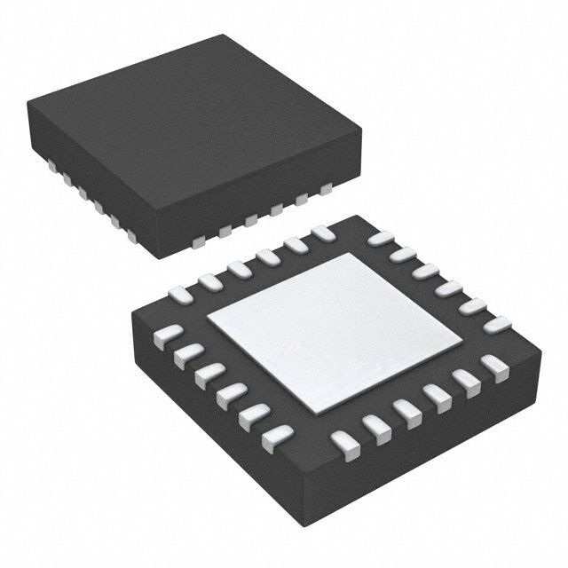
| 产品图片 |
|
| rohs | 符合RoHS无铅 / 符合限制有害物质指令(RoHS)规范要求 |
| 产品系列 | 电源管理 IC,开关控制器 ,Texas Instruments TPS51123RGETD-CAP™ |
| 数据手册 | |
| 产品型号 | TPS51123RGET |
| 产品 | Voltage Controllers |
| 产品目录页面 | |
| 产品种类 | 开关控制器 |
| 供应商器件封装 | 24-VQFN (4x4) |
| 其它名称 | 296-24069-6 |
| 功能 | 任何功能 |
| 包装 | Digi-Reel® |
| 单位重量 | 45.400 mg |
| 商标 | Texas Instruments |
| 安装类型 | 表面贴装 |
| 安装风格 | SMD/SMT |
| 封装 | Reel |
| 封装/外壳 | 24-VFQFN 裸露焊盘 |
| 封装/箱体 | VQFN-24 |
| 工作温度 | -40°C ~ 85°C |
| 工厂包装数量 | 250 |
| 带LED驱动器 | 无 |
| 带定序器 | 无 |
| 带监控器 | 无 |
| 开关频率 | 460 kHz |
| 拓扑 | 降压(降压)同步(2),线性(LDO)(2) |
| 拓扑结构 | Buck |
| 标准包装 | 1 |
| 电压-电源 | 5.5 V ~ 28 V |
| 电压/电流-输出1 | 控制器 |
| 电压/电流-输出2 | 控制器 |
| 电压/电流-输出3 | 3.3V,100mA |
| 类型 | DC/DC Switching Controllers |
| 系列 | TPS51123 |
| 输入电压 | 5.5 V to 28 V |
| 输出数 | 4 |
| 输出电压 | 5.5 V |
| 输出电流 | 20 A |
| 输出端数量 | 2 Output |
| 配用 | /product-detail/zh/TPS51123EVM-399/TPS51123EVM-399-ND/2232791 |
| 频率-开关 | 460kHz |


- 商务部:美国ITC正式对集成电路等产品启动337调查
- 曝三星4nm工艺存在良率问题 高通将骁龙8 Gen1或转产台积电
- 太阳诱电将投资9.5亿元在常州建新厂生产MLCC 预计2023年完工
- 英特尔发布欧洲新工厂建设计划 深化IDM 2.0 战略
- 台积电先进制程称霸业界 有大客户加持明年业绩稳了
- 达到5530亿美元!SIA预计今年全球半导体销售额将创下新高
- 英特尔拟将自动驾驶子公司Mobileye上市 估值或超500亿美元
- 三星加码芯片和SET,合并消费电子和移动部门,撤换高东真等 CEO
- 三星电子宣布重大人事变动 还合并消费电子和移动部门
- 海关总署:前11个月进口集成电路产品价值2.52万亿元 增长14.8%


PDF Datasheet 数据手册内容提取
TPS51123 www.ti.com SLUS890E–DECEMBER2008–REVISEDJANUARY2013 Dual-Synchronous, Step-Down Controller with Out-of-Audio™ Operation and 100-mA LDOs for Notebook System Power CheckforSamples:TPS51123 FEATURES APPLICATIONS 1 • Wide-InputVoltageRange:5.5Vto28V • NotebookComputers 2 • OutputVoltageRange:2Vto5.5V • I/OSupplies • Built-in100-mA5-V/3.3-VLDOwithSwitches • SystemPowerSupplies • Built-in1%2-VReferenceOutput DESCRIPTION • With/WithoutOut-of-Audio™ModeSelectable The TPS51123 is a cost effective, dual-synchronous Light-LoadandPWMonlyOperation buck controller targeted for notebook system power • Internal1.6-msVoltageServoSoftstart supply solutions. It provides 5-V and 3.3-V LDOs and • AdaptiveOn-TimeControlArchitecturewith requires few external components. The TPS51123 FourSelectableFrequencySetting supports high efficiency, fast transient responses and provides a combined power-good signal. Out-of- • 4500ppm/°CR CurrentSensing DS(on) Audio™ mode light-load operation enables low • Built-InOutputDischarge acoustic noise at much higher efficiency than • PowerGoodOutput conventional forced PWM operation. Adaptive on- • Built-inOVP/UVP/OCP time D-CAP™ control provides convenient and efficient operation. The part operates with supply • ThermalShutdown(Non-latch) input voltages ranging from 5.5 V to 28 V and • 24-PinQFN(RGE)Package supports output voltages from 2 V to 5.5 V. The TPS51123 is available in a 24-pin QFN package and is specified from -40°C to 85°C ambient temperature range. 13kW 20kW 20kW 30kW VIN VIN 220nF 130kW 130kW VIN 10mFx2 10mFx2 5.5V 6 5 4 3 2 1 to 2 2 L F 1 1 28V P B E E B P 7 VO2TRI VF ONS VR VF TRIVO1 24 10mF T 100kW 8 VREG3 PGOOD 23 VREG5 0.1mF 0.1mF 9 VBST2 TPS51123RGE VBST1 22 VO2 3.3mF 5.1W 10 DRVH2 (QFN-24) DRVH1 21 5.1W 3.3mF VO1 3.3V 11 LL2 PowerPAD LL1 20 5V 330mF 330mF L 12 DRVL2 E 5 DRVL1 19 S G EN0 SKIP GND VIN VRE ENC 13 14 15 16 17 18 EN0 ENC VREG5 33mF VIN UDG-08167 1 Pleasebeawarethatanimportantnoticeconcerningavailability,standardwarranty,anduseincriticalapplicationsof TexasInstrumentssemiconductorproductsanddisclaimerstheretoappearsattheendofthisdatasheet. Out-of-Audio,D-CAParetrademarksofTexasInstruments. 2 PRODUCTIONDATAinformationiscurrentasofpublicationdate. Copyright©2008–2013,TexasInstrumentsIncorporated Products conform to specifications per the terms of the Texas Instruments standard warranty. Production processing does not necessarilyincludetestingofallparameters.
TPS51123 SLUS890E–DECEMBER2008–REVISEDJANUARY2013 www.ti.com ORDERINGINFORMATION(1) ORDERABLE TRANSPORT MINIMUM T PACKAGE PINS ECOPLAN A DEVICES MEDIA QUANTITY PlasticQuadFlatPack TPS51123RGET 250 Green(RoHSandno -40°Cto85°C 24 Tape/Reel (QFN) TPS51123RGER 3000 Sb/Br) (1) Forthemostcurrentspcificationsandpackageinformation,seethePackageOptionAddendumlocatedattheendofthisdatasheetor refertoourwebsiteathttp://www.ti.com. ABSOLUTE MAXIMUM RATINGS(1) overoperatingfree-airtemperaturerange(unlessotherwisenoted) VALUE UNIT PARAMETER MIN MAX VBST1,VBST2 –0.3 36 VIN –0.3 30 LL1,LL2 –2.0 30 Inputvoltagerange (1) V LL1,LL2,pulsewidth<20ns –5.0 30 VBST1,VBST2 (2) –0.3 6 EN0,ENC,TRIP1,TRIP2,VFB1,VFB2,VO1,VO2,TONSEL,SKIPSEL –0.3 6 DRVH1,DRVH2 –1.0 36 Outputvoltagerange (1) DRVH1,DRVH2 (2) –0.3 6 V PGOOD,VREG3,VREG5,VREF,DRVL1,DRVL2 –0.3 6 HumanbodymodelQSS009-105(JESD22-A114A 2 Electrostaticdischarge kV ChargeddevicemodelQSS009-147(JESD22-C101B.01) 1.5 Junctiontemperaturerange,T –40 125 J Storagetemperature,T –55 150 °C stg (1) Stressesbeyondthoselistedunder"absolutemaximumratings"maycausepermanentdamagetothedevice.Thesearestressratings onlyandfunctionaloperationofthedeviceattheseoranyotherconditionsbeyondthoseindicatedunder"recommendedoperating conditions"isnotimplied.Exposuretoabsolute-maximum-ratedconditionsforextendedperiodsmayaffectdevicereliability. (2) VoltagevaluesarewithrespecttothecorrespondingLLxterminal. DISSIPATION RATINGS 2-oz.traceandcopperpadwithsolder. DERATINGFACTORABOVET PACKAGE T <25°CPOWERRATING A T =85°CPOWERRATING A =25°C A 24-pinRGE(1) 1.85W 18.5mW/°C 0.74W (1) Enhancedthermalconductanceby3x3thermalviasbeneaththermalpad. 2 SubmitDocumentationFeedback Copyright©2008–2013,TexasInstrumentsIncorporated ProductFolderLinks:TPS51123
TPS51123 www.ti.com SLUS890E–DECEMBER2008–REVISEDJANUARY2013 RECOMMENDED OPERATING CONDITIONS overoperatingfree-airtemperaturerange(unlessotherwisenoted) PARAMETER MIN TYP MAX UNIT Supplyvoltage VIN 5.5 28 VBST1,VBST2 -0.1 34 VBST1,VBST2(wrtLLx) -0.1 5.5 Inputvoltagerange EN0,ENC,TRIP1,TRIP2,VFB1,VFB2,VO1,VO2,TONSEL, -0.1 5.5 SKIPSEL V DRVH1,DRVH2 -0.8 34 DRVH1,DRVH2(wrtLLx) -0.1 5.5 Outputvoltagerange LL1,LL2 -1.8 28 VREF,VREG3,VREG5 -0.1 5.5 PGOOD,DRVL1,DRVL2 -0.1 5.5 T Operatingfree-airtemperature -40 85 °C A Copyright©2008–2013,TexasInstrumentsIncorporated SubmitDocumentationFeedback 3 ProductFolderLinks:TPS51123
TPS51123 SLUS890E–DECEMBER2008–REVISEDJANUARY2013 www.ti.com ELECTRICAL CHARACTERISTICS overoperatingfree-airtemperaturerange,VIN=12V(unlessotherwisenoted) PARAMETER CONDITIONS MIN TYP MAX UNIT SUPPLYCURRENT VINcurrent,T =25°C,noload,VO1=0V, A I VINsupplycurrent1 VO2=0V,EN0=open,ENC=5V, 0.55 1 mA VIN1 TRIP1=TRIP2=2V,VFB1=VFB2=2.05V VINcurrent,T =25°C,noload,VO1=5V, A I VINsupplycurrent2 VO2=3.3V,EN0=open,ENC=5V, 4 6.5 μA VIN2 TRIP1=TRIP2=2V,VFB1=VFB2=2.05V VO1current,T =25°C,noload,VO1=5V, A I VO1current VO2=3.3V,EN0=open,ENC=5V, 0.8 1.5 mA VO1 TRIP1=TRIP2=2V,VFB1=VFB2=2.05V VO2current,T =25°C,noload,VO1=5V, A I VO2current VO2=3.3V,EN0=open,ENC=5V, 12 100 VO2 TRIP1=TRIP2=2V,VFB1=VFB2=2.05V VINcurrent,T =25°C,noload, μA I VINstandbycurrent A 95 250 VINSTBY EN0=1.2V,ENC=0V VINcurrent,T =25°C,noload, I VINshutdowncurrent A 10 25 VINSDN EN0=ENC=0V VREFOUTPUT I =0A 1.98 2.00 2.02 VREF V VREFoutputvoltage V VREF –5μA<I <100μA 1.97 2.00 2.03 VREF VREG5OUTPUT VO1=0V,I <100mA,T =25°C 4.8 5 5.2 VREG5 A VO1=0V,I <100mA, V VREG5outputvoltage VREG5 4.75 5 5.25 V VREG5 6.5V<VIN<28V VO1=0V,I <50mA,5.5V<VIN<28V 4.75 5 5.25 VREG5 I VREG5outputcurrent VO1=0V,VREG5=4.5V 100 175 250 mA VREG5 Turnson 4.55 4.7 4.85 V Switchoverthreshold V TH5VSW Hysteresis 0.15 0.25 0.3 R 5VSWR VO1=5V,I =100mA 1 3 Ω 5VSW ON VREG5 VREG3OUTPUT VO2=0V,I <100mA,T =25°C 3.2 3.33 3.46 VREG3 A V VREG3outputvoltage VO2=0V,I <100mA,6.5V<VIN<28V 3.13 3.33 3.5 V VREG3 VREG3 VO2=0V,I <50mA,5.5V<VIN<28V 3.13 3.33 3.5 VREG3 I VREG3outputcurrent VO2=0V,VREG3=3V 100 175 250 mA VREG3 Turnson 3.05 3.15 3.25 V Switchoverthreshold V TH3VSW Hysteresis 0.1 0.2 0.25 R 3VSWR VO2=3.3V,I =100mA 1.5 4 Ω 3VSW ON VREG3 INTERNALREFERENCEVOLTAGE V Internalreferencevoltage I =0A,beginningofONstate 1.95 1.98 2.01 IREF VREF FBvoltage,I =0A,skipmode 1.98 2.01 2.04 VREF FBvoltage,I =0A,skipmode,T =25°C 1.9849 2.01 2.0351 VREF A V VVFB VFBregulationvoltage FBvoltage,IVREF=0A,OOAmode (1) 2.00 2.035 2.07 FBvoltage,I =0A,continuousconduction mode(1) VREF 2.00 I VFBinputcurrent VFBx=2.0V,T =25°C -20 20 nA VFB A OUTPUTVOLTAGE,V DISCHARGE OUT I VOUTdischargecurrent ENC=0V,VOx=0.5V 10 60 mA Dischg (1) Ensuredbydesign.Notproductiontested. 4 SubmitDocumentationFeedback Copyright©2008–2013,TexasInstrumentsIncorporated ProductFolderLinks:TPS51123
TPS51123 www.ti.com SLUS890E–DECEMBER2008–REVISEDJANUARY2013 ELECTRICAL CHARACTERISTICS (continued) overoperatingfree-airtemperaturerange,VIN=12V(unlessotherwisenoted) PARAMETER CONDITIONS MIN TYP MAX UNIT OUTPUTDRIVERS Source,V =100mV 4 8 BSTx-DRVHx R DRVHresistance DRVH Sink,V =100mV 1.5 4 DRVHx-LLx Ω Source,V =100mV 4 8 VREG5-DRVLx R DRVLresistance DRVL Sink,V =100mV 1.5 4 DRVLx DRVHx-offtoDRVLx-on 10 t Deadtime ns DEAD DRVLx-offtoDRVHx-on 30 INTERNALBSTDIODE V Forwardvoltage V ,I =10mA,T =25°C 0.7 0.8 0.9 V FBST VREG5-VBSTx F A I VBSTleakagecurrent VBSTx=34V,LLx=28V,T =25°C 0.1 1 μA VBSTLK A DUTYANDFREQUENCYCONTROL t CH1on-time1 V =12V,VO1=5V,200kHzsetting 2080 ON11 IN t CH1on-time2 V =12V,VO1=5V,245kHzsetting 1700 ON12 IN t CH1on-time3 V =12V,VO1=5V,300kHzsetting 1390 ON13 IN t CH1on-time4 V =12V,VO1=5V,365kHzsetting 1140 ON14 IN t CH2on-time1 V =12V,VO2=3.3V,250kHzsetting 1100 ON21 IN ns t CH2on-time2 V =12V,VO2=3.3V,305kHzsetting 900 ON22 IN t CH2on-time3 V =12V,VO2=3.3V,375kHzsetting 730 ON23 IN t CH2on-time4 V =12V,VO2=3.3V,460kHzsetting 600 ON24 IN t Minimumon-time T =25°C 80 ON(min) A t Minimumoff-ime T =25°C 300 OFF(min) A SOFTSTART t InternalSStime Internalsoftstart 1.1 1.6 2.1 ms SS POWERGOOD PGinfromlower 92.50% 95% 97.50% V PGthreshold PGinfromhigher 102.50% 105% 107.50% THPG PGhysteresis 2.50% 5% 7.50% I PGsinkcurrent PGOOD=0.5V 5 12 mA PGMAX t PGdelaytime DelayforPGin 350 510 670 μs PGDEL LOGICTHRESHOLDANDSETTINGCONDITIONS Shutdown 0.4 V EN0settingvoltage V EN0 Enable 2.4 I EN0current V =0.2V 2 3.5 5 μA EN0 EN0 Shutdown 0.6 V ENCthresholdvoltage V ENC Enable 2 200kHz/250kHz 1.5 245kHz/305kHz 1.9 2.1 V TONSELsettingvoltage V TONSEL 300kHz/375kHz 2.7 3.6 365kHz/460kHz 4.7 Autoskip 1.5 V SKIPSELsettingvoltage PWMonly 1.9 2.1 V SKIPSEL OOAautoskip 2.7 Copyright©2008–2013,TexasInstrumentsIncorporated SubmitDocumentationFeedback 5 ProductFolderLinks:TPS51123
TPS51123 SLUS890E–DECEMBER2008–REVISEDJANUARY2013 www.ti.com ELECTRICAL CHARACTERISTICS (continued) overoperatingfree-airtemperaturerange,VIN=12V(unlessotherwisenoted) PARAMETER CONDITIONS MIN TYP MAX UNIT PROTECTION:CURRENTSENSE I TRIPxsourcecurrent V =920mV,T =25°C 9.4 10 10.6 μA TRIP TRIPx A TRIPxcurrenttemperature TC Onthebasisof25°C 4500 ppm/°C ITRIP coefficient ((V /9)-24mV-V )voltage,V V OCPcomparatoroffset TRIPx-GND GND-LLx TRIPx- -8 0 8 OCLoff =920mV GND V MaximumOCLsetting V =5V 185 205 225 mV OCL(max) TRIPx Zerocrossdetection V V voltage -5 0 5 ZC comparatoroffset GND-LLx V Currentlimitthreshold V voltage (2) 0.515 2 V TRIP TRIPx-GND PROTECTION:UNDERVOLTAGEANDOVERVOLTAGEPROTECTION V OVPtripthreshold OVPdetect 110% 115% 120% OVP t OVPpropdelay 2 μs OVPDEL UVPdetect 55% 60% 65% V OutputUVPtripthreshold UVP Hysteresis 10% t OutputUVPpropdelay 20 32 40 μs UVPDEL t OutputUVPenabledelay 1.4 2 2.6 ms UVPEN UNDERVOLTAGELOCKOUT(UVLO) Wakeup 4.1 4.2 4.3 V VREG5UVLOthreshold UVVREG5 Hysteresis 0.38 0.43 0.48 V V VREG3UVLOthreshold Shutdown (2) VO2-1 UVVREG3 THERMALSHUTDOWN Shutdowntemperature (2) 150 T Thermalshutdownthreshold °C SDN Hysteresis (2) 10 (2) Ensuredbydesign.Notproductiontested. 6 SubmitDocumentationFeedback Copyright©2008–2013,TexasInstrumentsIncorporated ProductFolderLinks:TPS51123
TPS51123 www.ti.com SLUS890E–DECEMBER2008–REVISEDJANUARY2013 DEVICE INFORMATION Table1. TERMINALFUNCTIONSTABLE TERMINAL I/O DESCRIPTION NAME NO. DRVH1 21 O High-sideN-channelMOSFETdriveroutputs.LLreferenceddrivers. DRVH2 10 DRVL1 19 O Low-sideN-channelMOSFETdriveroutputs.GNDreferenceddrivers. DRVL2 12 Masterenableinput. EN0 13 I/O Open:LDOson,andreadytoturnbothswitcherchannels. GND:disableallcircuit Channel1andChannel2enableinput.Pulluptothevoltageranging3.3-Vto5-Vtoturnonboth ENC 18 I switcherchannels.Shorttogroundtoshutdownthem. GND 15 – Ground. LL1 20 I Switchnodeconnectionsforhigh-sidedrivers,currentlimitandcontrolcircuitry. LL2 11 PGOOD 23 O Powergoodwindowcomparatoroutputforchannel1and2.(LogicalAND) Selectionpinforoperationmode: OOAautoskip:ConnecttoVREG3orVREG5 SKIPSEL 14 I PWMonly:ConnecttoVREF Autoskip:ConnecttoGND TRIP1 1 I/O OCLtripsettingpins.ConnectresistorfromthispintoGNDtosetthresholdforsynchronousR DS(on) TRIP2 6 sense. On-timeadjustmentpin. 365kHz/460kHzsetting:connecttoVREG5 TONSEL 4 I 300kHz/375kHzsetting:connecttoVREG3 245kHz/305kHzsetting:connecttoVREF 200kHz/250kHzsetting:connecttoGND VBST1 22 I Supplyinputforhigh-sideN-channelMOSFETdriver(boostterminal). VBST2 9 VFB1 2 I SMPSfeedbackinputs.Connectwithfeedbackresistordivider. VFB2 5 VIN 16 I Highvoltagepowersupplyinputfor5-V/3.3-VLDO. VO1 24 OutputconnectiontoSMPS.Theseterminalsworkasfixedvoltageinputsandoutputdischarge I/O VO2 7 inputs.VO1andVO2alsoworkas5-Vand3.3-Vswitchoverreturnpowerinputrespectively. 2-Vreferencevoltageoutput.Connect220-nFto1-μFceramiccapacitortoSignalGNDnearthe VREF 3 O device. 3.3-Vpowersupplyoutput.Connecta10-μFceramiccapacitortoPowerGNDnearthedevice.A1- VREG3 8 O μFceramiccapacitorisacceptablewhennotloaded. VREG5 17 O 5-Vpowersupplyoutput.Connecta33-μFceramiccapacitortoPowerGNDnearthedevice. Copyright©2008–2013,TexasInstrumentsIncorporated SubmitDocumentationFeedback 7 ProductFolderLinks:TPS51123
TPS51123 SLUS890E–DECEMBER2008–REVISEDJANUARY2013 www.ti.com QFNPACKAGE(TOPVIEW) VO1 PGOOD VBST1 DRVH1 LL1 DRVL1 24 23 22 21 20 19 TRIP1 1 18 ENC VFB1 2 17 VREG5 VREF 3 TPS51123RGE 16 VIN (QFN-24) TONSEL 4 15 GND VFB2 5 14 SKIPSEL TRIP2 6 13 EN0 7 8 9 10 11 12 VO2 VREG3 VBST2 DRVH2 LL2 DRVL2 FunctionalBlockDiagram 8 SubmitDocumentationFeedback Copyright©2008–2013,TexasInstrumentsIncorporated ProductFolderLinks:TPS51123
TPS51123 www.ti.com SLUS890E–DECEMBER2008–REVISEDJANUARY2013 SwitcherControllerBlock Copyright©2008–2013,TexasInstrumentsIncorporated SubmitDocumentationFeedback 9 ProductFolderLinks:TPS51123
TPS51123 SLUS890E–DECEMBER2008–REVISEDJANUARY2013 www.ti.com TYPICAL CHARACTERISTICS VINSUPPLYCURRENT1 VINSUPPLYCURRENT1 vs vs JUNCTIONTEMPERATURE INPUTVOLTAGE 800 800 700 700 A A m m 600 - 600 - urrent1 500 urrent1 500 C C NSupply 340000 NSupply 340000 VI VI - 200 - IVIN1 100 IVIN1 200 100 0 -50 0 50 100 150 0 TJ -JunctionTemperature- °C 5 10 15 20 25 VIN-InputVoltage-V Figure1. Figure2. VINSUPPLYCURRENT2 VINSUPPLYCURRENT2 vs vs JUNCTIONTEMPERATURE INPUTVOLTAGE 9 9 8 8 mA 7 Am 7 - - 2 2 nt 6 nt 6 e e Curr 5 Curr 5 y y pl pl p 4 p 4 u u S S VIN 3 VIN 3 - - IVIN2 2 IVIN2 2 1 1 0 0 -50 0 50 100 150 5 10 15 20 25 TJ -JunctionTemperature- °C VIN-InputVoltage-V Figure3. Figure4. 10 SubmitDocumentationFeedback Copyright©2008–2013,TexasInstrumentsIncorporated ProductFolderLinks:TPS51123
TPS51123 www.ti.com SLUS890E–DECEMBER2008–REVISEDJANUARY2013 TYPICAL CHARACTERISTICS (continued) VIN STANDBYCURRENT VINSTANDBYCURRENT vs vs INPUT VOLTAGE JUNCTIONTEMPERATURE 250 250 Am 200 nA 200 - nt- ent Curre 150 Curr 150 y y b b d VINStand 100 VINStan 100 I-VINSTBY 50 I-VINSTBY 50 0 0 - 0 50 100 150 5 10 15 20 25 50 TJ -JunctionTemperature-°C VIN- Input Voltage - V Figure5. Figure6. VINSHUTDOWNCURRENT VINSHUTDOWNCURRENT vs vs JUNCTIONTEMPERATURE INPUTVOLTAGE 25 25 A Am 20 m 20 - - nt nt e e urr urr C 15 C 15 n n w w o o d d Shut 10 Shut 10 N N VI VI - - N N D D NS 5 NS 5 IVI IVI 0 0 -50 0 50 100 150 5 10 15 20 25 TJ -JunctionTemperature- °C VIN-InputVoltage-V Figure7. Figure8. Copyright©2008–2013,TexasInstrumentsIncorporated SubmitDocumentationFeedback 11 ProductFolderLinks:TPS51123
TPS51123 SLUS890E–DECEMBER2008–REVISEDJANUARY2013 www.ti.com TYPICAL CHARACTERISTICS (continued) SWITCHING FREQUENCY CURRENTSENSECURRENT vs vs INPUT VOLTAGE JUNCTIONTEMPERATURE 500 14 TONSEL= GND 13 Am Hz 400 k - 12 - urrent 11 uency 300 C q ense 10 gFre CH2 S n Current 9 withchi 200 CH1 S -TRIP 8 f-SW100 I 7 0 6 - 6 8 10 12 14 16 18 20 22 24 26 0 50 100 150 50 TJ -JunctionTemperature- °C VIN- Input Voltage - V Figure9. Figure10. SWITCHING FREQUENCY SWITCHING FREQUENCY vs vs INPUT VOLTAGE INPUT VOLTAGE 500 500 TONSEL= 2V TONSEL= 3.3V Hz 400 Hz 400 CH2 k k - - ncy CH2 ncy ue 300 ue 300 q q Fre Fre CH1 g g hchin 200 CH1 hchin 200 wit wit S S f-SW100 f-SW100 0 0 6 8 10 12 14 16 18 20 22 24 26 6 8 10 12 14 16 18 20 22 24 26 VIN- Input Voltage - V VIN- Input Voltage - V Figure11. Figure12. 12 SubmitDocumentationFeedback Copyright©2008–2013,TexasInstrumentsIncorporated ProductFolderLinks:TPS51123
TPS51123 www.ti.com SLUS890E–DECEMBER2008–REVISEDJANUARY2013 TYPICAL CHARACTERISTICS (continued) SWITCHING FREQUENCY SWITCHING FREQUENCY vs vs INPUT VOLTAGE OUTPUT CURRENT 500 500 TONSEL= GND CH2 TONSEL= 5V Hz 400 Hz 400 k k - - ncy CH1 ncy ue 300 ue 300 q q Fre Fre CH2 PWM Only g g n n hi 200 hi 200 c c h h wit wit CH1 PWM Only CH2Auto-skip S S - - fSW100 fSW100 CH2 OOA CH1 OOA CH1Auto-skip 0 0 6 8 10 12 14 16 18 20 22 24 26 0.001 0.01 0.1 1 10 V - Input Voltage - V I - Output Current -A IN OUT Figure13. Figure14. SWITCHING FREQUENCY SWITCHING FREQUENCY vs vs OUTPUT CURRENT OUTPUT CURRENT 500 500 TONSEL= 2V TONSEL= 3.3V Hz 400 Hz 400 CH2 PWM Only k k uency- 300 CH2 PWM Only uency- 300 Freq Freq CH1 PWM Only g g withchin 200 CH1 PWM OnClyH2Auto-skip withchin 200 CH2Auto-skip S S f-SW100 CH2 OOA f-SW100 CH1 OOA CH2 OOA CH1 OOA CH1Auto-skip CH1Auto-skip 0 0 0.001 0.01 0.1 1 10 0.001 0.01 0.1 1 10 IOUT- Output Current -A IOUT- Output Current -A Figure15. Figure16. Copyright©2008–2013,TexasInstrumentsIncorporated SubmitDocumentationFeedback 13 ProductFolderLinks:TPS51123
TPS51123 SLUS890E–DECEMBER2008–REVISEDJANUARY2013 www.ti.com TYPICAL CHARACTERISTICS (continued) SWITCHING FREQUENCY vs OVP/UVPTHRESHOLDVOLTAGE OUTPUT CURRENT vs JUNCTIONTEMPERATURE 500 150 TONSEL= 5V 140 CH2 PWM Only Hz 400 % 130 y-k old- 120 c h n CH1 PWM Only s Freque 300 VPThre 110100 g U hin 200 VP/ 90 c O -SwithW100 CHC2H O2OAAuto-skip -P/VUVP 7800 fS CH1 OOA VOV 60 CH1Auto-skip 50 0 40 0.001 0.01 0.1 1 10 -50 0 50 100 150 IOUT- Output Current -A TJ -JunctionTemperature- °C Figure17. Figure18. VREG5OUTPUTVOLTAGE VREG3OUTPUTVOLTAGE vs vs OUTPUTCURRENT OUTPUTCURRENT 5.05 3.35 V V Voltage-5.00 Voltage- 3.3 Output Output VREG54.95 VREG33.25 V-VREG5 V-VREG3 4.90 3.2 0 20 40 60 80 100 0 20 40 60 80 100 IVREG5-VREG5OutputCurrent-mA IVREG3-VREG3OutputCurrent-mA Figure19. Figure20. 14 SubmitDocumentationFeedback Copyright©2008–2013,TexasInstrumentsIncorporated ProductFolderLinks:TPS51123
TPS51123 www.ti.com SLUS890E–DECEMBER2008–REVISEDJANUARY2013 TYPICAL CHARACTERISTICS (continued) VREFOUTPUTVOLTAGE 5-VOUTPUTVOLTAGE vs vs OUTPUTCURRENT OUTPUTCURRENT 5.075 2.020 OOA 2.015 5.050 V V - - e 2.010 e g g a a Volt 2.005 Volt 5.025 Auto-skip ut ut p p ut 2.000 ut O O F V 5.000 PWMOnly RE 1.995 5- -VEF 1.990 V-OUT1 4.975 R V V 1.985 4.950 1.980 0.001 0.01 0.1 1 10 0 20 40 60 80 100 I -5-VOutputCurrent-A OUT1 IVREF-VREFOutputCurrent-mA Figure21. Figure22. 3.3-V OUTPUT VOLTAGE 5-V OUTPUT VOLTAGE vs vs OUTPUT CURRENT INPUT VOLTAGE 3.360 5.075 OOA Voltage-V 3.330 Auto-skip Voltage-V 55..002550 IO= 0A Output 3.300 PWM Only Output 3.3-V -5-V 5.000 V-OUT23.270 VOUT14.975 IO= 6A 3.240 4.950 0.001 0.01 0.1 1 10 6 8 10 12 14 16 18 20 22 24 26 IOUT2- 3.3-V Output Current -A VIN- Input Voltage - V Figure23. Figure24. Copyright©2008–2013,TexasInstrumentsIncorporated SubmitDocumentationFeedback 15 ProductFolderLinks:TPS51123
TPS51123 SLUS890E–DECEMBER2008–REVISEDJANUARY2013 www.ti.com TYPICAL CHARACTERISTICS (continued) 3.3-V OUTPUT VOLTAGE 5-VEFFICIENCY vs vs OUTPUTCURRENT INPUT VOLTAGE 100 3.360 Auto-Skip 80 V - 3.330 e g V =20V a % IN Volt IO= 0A y– 60 ut nc VOutp 3.300 IO= 6A Efficie 40 VIN=12V 3- – 3. h - VOUT23.270 20 OOA VIN=8V PWMOnly 3.240 0 6 8 10 12 14 16 18 20 22 24 26 0.001 0.01 0.1 1 10 V - Input Voltage - V IN I –5-VOutputCurrent–A OUT1 Figure25. Figure26. 3.3-VEFFICIENCY vs OUTPUTCURRENT 100 Auto-skip 80 % - 60 VIN=8V y c n e VIN=12V ci Effi 40 VIN=20V - h 20 OOA PWMOnly 5-VSwitcherON 0 0.001 0.01 0.1 1 10 I -3.3-VOutputCurrent-A OUT2 Figure27. 16 SubmitDocumentationFeedback Copyright©2008–2013,TexasInstrumentsIncorporated ProductFolderLinks:TPS51123
TPS51123 www.ti.com SLUS890E–DECEMBER2008–REVISEDJANUARY2013 TYPICAL CHARACTERISTICS (continued) 5-VLoadTransientResponse 3.3-VLoadTransientResponse VOUT1(100mV/div) VOUT2(100mV/div) IIND(5A/div) IIND(5A/div) IOUT1(5A/div) IOUT2(5A/div) Figure28. Figure29. 5-VStartupWaveforms 3.3-VStartupWaveforms ENC(5V/div) ENC(5V/div) V (2V/div) OUT1 V (2V/div) OUT2 PGOOD(5V/div) PGOOD(5V/div) Figure30. Figure31. Copyright©2008–2013,TexasInstrumentsIncorporated SubmitDocumentationFeedback 17 ProductFolderLinks:TPS51123
TPS51123 SLUS890E–DECEMBER2008–REVISEDJANUARY2013 www.ti.com TYPICAL CHARACTERISTICS (continued) 5-VSwitchoverWaveforms 3.3-VSwitchoverWaveforms VREG5(200mV/div) VREG3(200mV/div) VOUT1(200mV/div) VOUT2(200mV/div) Figure32. Figure33. 5-VSoft-stopWaveforms 3.3-VSoft-stopWaveforms ENC(10V/div) ENC(10V/div) V (2V/div) V (2V/div) OUT1 OUT2 PGOOD(5V/div) PGOOD(5V/div) DRVL1(5V/div) DRVL2(5V/div) Figure34. Figure35. 18 SubmitDocumentationFeedback Copyright©2008–2013,TexasInstrumentsIncorporated ProductFolderLinks:TPS51123
TPS51123 www.ti.com SLUS890E–DECEMBER2008–REVISEDJANUARY2013 APPLICATION INFORMATION PWM Operations The main control loop of the switch mode power supply (SMPS) is designed as an adaptive on-time pulse width modulation (PWM) controller. It supports a proprietary D-CAP™ mode. D-CAP™ mode does not require external compensation circuit and is suitable for low external component count configuration when used with appropriate amountofESRattheoutputcapacitor(s). At the beginning of each cycle, the synchronous top MOSFET is turned on, or becomes ‘ON’ state. This MOSFET is turned off, or becomes ‘OFF’ state, after internal one shot timer expires. This one shot is determined by V and V to keep frequency fairly constant over input voltage range, hence it is called adaptive on-time IN OUT control.TheMOSFETisturnedonagainwhenthefeedbackpointvoltage,VFB,decreasedtomatchwithinternal 2-V reference. The inductor current information is also monitored and should be below the over current threshold to initiate this new cycle. Repeating operation in this manner, the controller regulates the output voltage. The synchronous bottom or the “rectifying” MOSFET is turned on at the beginning of each ‘OFF’ state to keep the conductionlossminimum.TherectifyingMOSFETisturnedoffbeforethetopMOSFETturnsonatnextswitching cycle or when inductor current information detects zero level. In the auto-skip mode or the OOA skip mode, this enables seamless transition to the reduced frequency operation at light load condition so that high efficiency is keptoverbroadrangeofloadcurrent. Adaptive On-Time Control and PWM Frequency TPS51123 does not have a dedicated oscillator on board. However, the part runs with pseudo-constant frequency by feed-forwarding the input and output voltage into the on-time, one-shot timer. The on-time is controlledinverseproportionaltotheinputvoltageandproportionaltotheoutputvoltagesothatthedutyratiowill be kept as VOUT/VIN technically with the same cycle time. The frequencies are set by TONSEL terminal connectionasTable2. Table2.TONSELConnectionandSwitchingFrequency SWITCHINGFREQUENCY(kHz) TONSELCONNECTION CH1 CH2 GND 200 250 VREF 245 305 VREG3 300 375 VREG5 365 460 Copyright©2008–2013,TexasInstrumentsIncorporated SubmitDocumentationFeedback 19 ProductFolderLinks:TPS51123
TPS51123 SLUS890E–DECEMBER2008–REVISEDJANUARY2013 www.ti.com Loop Compensation Fromsmall-signalloopanalysis,abuckconverterusingD-CAPTMmodecanbesimplifiedasbelow. VIN R1 DRVH Lx PWM VFB Control logic + & I Ic Io + Driver DRVL L R2 2V ESR Vc RL VoltageDivider SwitchingModulator Co OutputCapacitor Figure36. SimplifyingtheModulator The output voltage is compared with internal reference voltage after divider resistors, R1 and R2. The PWM comparator determines the timing to turn on high-side MOSFET. The gain and speed of the comparator is high enough to keep the voltage at the beginning of each on cycle substantially constant. For the loop stability, the 0dBfrequency,f ,definedbelowneedtobelowerthan1/4oftheswitchingfrequency. 0 1 f f = £ SW 0 2p´ESR´C 4 O (1) As f is determined solely by the output capacitor's characteristics, loop stability of D-CAPTM mode is determined 0 by the capacitor's chemistry. For example, specialty polymer capacitors (SP-CAP) have Co in the order of several 100 μF and ESR in range of 10 mΩ. These make f on the order of 100 kHz or less and the loop will be 0 stable. However, ceramic capacitors have f at more than 700 kHz, which is not suitable for this operational 0 mode. Ramp Signal TheTPS51123addsarampsignaltothe2-Vreferenceinordertoimproveitsjitterperformance.Asdescribedin the previous section, the feedback voltage is compared with the reference information to keep the output voltage in regulation. By adding a small ramp signal to the reference, the S/N ratio at the onset of a new switching cycle is improved. Therefore the operation becomes less jitter and stable. The ramp signal is controlled to start with - 20mV at the beginning of ON-cycle and to become 0 mV at the end of OFF-cycle in steady state. By using this scheme,theTPS51123improvejitterperformancewithoutsacrificingthereferenceaccuracy. 20 SubmitDocumentationFeedback Copyright©2008–2013,TexasInstrumentsIncorporated ProductFolderLinks:TPS51123
TPS51123 www.ti.com SLUS890E–DECEMBER2008–REVISEDJANUARY2013 Light Load Condition in Auto-Skip Operation The TPS51123 automatically reduces switching frequency at light load conditions to maintain high efficiency. This reduction of frequency is achieved smoothly and without increase of V ripple. Detail operation is OUT described as follows. As the output current decreases from heavy load condition, the inductor current is also reduced and eventually comes to the point that its ‘valley’ touches zero current, which is the boundary between continuous conduction and discontinuous conduction modes. The rectifying MOSFET is turned off when this zero inductor current is detected. As the load current further decreased, the converter runs in discontinuous conduction mode and it takes longer and longer to discharge the output capacitor to the level that requires next ‘ON’cycle.TheONtimeiskeptthesameasthatintheheavyloadcondition.Inreverse,whentheoutputcurrent increase from light load to heavy load, switching frequency increases to the preset value as the inductor current reaches to the continuous conduction. The transition load point to the light load operation I (i.e. the OUT(LL) thresholdbetweencontinuousanddiscontinuousconductionmode)canbecalculatedasfollows; 1 (VIN-VOUT)´VOUT I = ´ OUT(LL) 2´L´f V IN (2) wherefisthePWMswitchingfrequency. Switching frequency versus output current in the light load condition is a function of L, V and V , but it IN OUT decreases almost proportional to the output current from the I shown in Equation 2. For example, it ise 60 OUT(LL) kHzatI /5ifthefrequencysettingis300kHz. OUT(LL) Out-of-Audio™ Light-Load Operation Out-of-Audio™ (OOA) light-load mode is a unique control feature that keeps the switching frequency above acoustic audible frequencies toward virtually no load condition while maintaining best of the art high conversion efficiency. When the Out-of-Audio™ operation is selected, OOA control circuit monitors the states of both MOSFET and force to change into the ‘ON’ state if both of MOSFETs are off for more than 32 μs. This means that the top MOSFET is turned on even if the output voltage is higher than the target value so that the output capacitoristendstobeovercharged. The OOA control circuit detects the over-voltage condition and begins to modulate the on time to keep the output voltageregulated.Asaresult,theoutputvoltagebecomes0.5%higherthannormallight-loadoperation. Enable and Soft Start EN0 is the control pin of VREG5, VREG3 and VREF regulators. Bring this node down to GND disables those three regulators and minimize the shutdown supply current to 10 μA. Pulling this node up to 3.3 V or 5 V will turn the three regulators on to standby mode. The two switch mode power supplies (channel-1, channel-2) become ready to enable at this standby mode. The TPS51123 has an internal, 1.6 ms, voltage servo softstart for each channel. When the ENC pin becomes higher than the enable threshold voltage, which is typically 1.26 V, an internal DAC begins ramping up the reference voltage to both of the PWM comparators at the same time. Smoothcontroloftheoutputvoltageismaintainedduringstartup. Table3.EnablingState EN0 ENC VREF VREG5 VREG3 CH1 CH2 GND Don’tCare Off Off Off Off Off Open Off On On On Off Off Open On On On On On On VREG5/VREG3 Linear Regulators There are two sets of 100-mA standby linear regulators which outputs 5 V and 3.3 V, respectively. The VREG5 serves as the main power supply for the analog circuitry of the device and provides the current for gate drivers. TheVREG3isintendedmainlyforauxiliary3.3-Vsupplyforthenotebooksystemduringstandbymode. Add a ceramic capacitor with a value of at least 33 μF and place it close to the VREG5 pin, and add at most 10μFtotheVREG3pin.TotalcapacitanceconnectedtotheVREG3pinshouldnotexceed10μF. Copyright©2008–2013,TexasInstrumentsIncorporated SubmitDocumentationFeedback 21 ProductFolderLinks:TPS51123
TPS51123 SLUS890E–DECEMBER2008–REVISEDJANUARY2013 www.ti.com VREG5 Switch Over When the VO1 voltage becomes higher than 4.7 V AND channel-1 internal powergood flag is generated, internal 5-V LDO regulator is shut off and the VREG5 output is connected to VO1 by internal switch over MOSFET. The 510-μspowergooddelayhelpsaswitchoverwithoutglitch. VREG3 Switch Over When the VO2 voltage becomes higher than 3.15 V AND channel-2 internal powergood flag is generated, internal 3.3-V LDO regulator is shut off and the VREG3 output is connected to VO2 by internal switch over MOSFET.The510-μspowergooddelayhelpsaswitchoverwithoutglitch. Powergood The TPS51123 has one powergood output that indicates 'high' when both switcher outputs are within the targets (AND gated). The powergood function is activated with 2-ms internal delay after ENC goes high. If the output voltage becomes within ±5% of the target value, internal comparators detect power good state and the powergood signal becomes high after 510-μs internal delay. Therefore PGOOD goes high around 2.5 ms after ENC goes high. If the output voltage goes outside of ±10% of the target value, the powergood signal becomes low after 2-μs internal delay. The powergood output is an open drain output and is needed to be pulled up outside. Also note that, in the case of Auto-skip or Out-of-Audio™ mode, if the output voltage goes +10% above the target value and the power-good signal flags low, then the loop attempts to correct the output by turning on the low-side driver (forced PWM mode). After the feedback voltage returns to be within +5% of the target value and thepower-goodsignalgoeshigh,thecontrollerreturnsbacktoauto-skipmodeorOut-of-Audio™mode. Output Discharge Control When ENC is low, the TPS51123 discharges outputs using internal MOSFET which is connected to VOx and GND.ThecurrentcapabilityoftheseMOSFETsislimitedtodischargeslowly. Low-Side Driver The low-side driver is designed to drive high current low R N-channel MOSFET(s). The drive capability is DS(on) represented by its internal resistance, which are 4 Ω for VREG5 to DRVLx and 1.5 Ω for DRVLx to GND. A dead time to prevent shoot through is internally generated between top MOSFET off to bottom MOSFET on, and bottom MOSFET off to top MOSFET on. 5-V bias voltage is delivered from VREG5 supply. The instantaneous drive current is supplied by an input capacitor connected between VREG5 and GND. The average drive current is equal to the gate charge at Vgs = 5 V times switching frequency. This gate drive current as well as the high- sidegatedrivecurrenttimes5VmakesthedrivingpowerwhichneedtobedissipatedfromTPS51123package. High-Side Driver The high-side driver is designed to drive high current, low R N-channel MOSFET(s). When configured as a DS(on) floating driver, 5-V bias voltage is delivered from VREG5 supply. The average drive current is also calculated by the gate charge at Vgs = 5 V times switching frequency. The instantaneous drive current is supplied by the flying capacitorbetweenVBSTxandLLxpins.Thedrivecapabilityisrepresentedbyitsinternalresistance,whichare4 ΩforVBSTxtoDRVHxand1.5Ω forDRVHxtoLLx. 22 SubmitDocumentationFeedback Copyright©2008–2013,TexasInstrumentsIncorporated ProductFolderLinks:TPS51123
TPS51123 www.ti.com SLUS890E–DECEMBER2008–REVISEDJANUARY2013 Current Protection TPS51123 has cycle-by-cycle over current limiting control. The inductor current is monitored during the ‘OFF’ state and the controller keeps the ‘OFF’ state during the inductor current is larger than the over current trip level. In order to provide both good accuracy and cost effective solution, TPS51123 supports temperature compensated MOSFET R sensing. The TRIPx pin should be connected to GND through the trip voltage DS(on) settingresistor,R .TRIPxterminalsourcesI current,whichis10μAtypicallyatroomtemperature,andthe TRIP TRIP trip level is set to the OCL trip voltage V as below. Note that the V is limited up to about 205 mV TRIP TRIP internally. VTRIP(mV)= RTRIP(kW)´ITRIP(mA)-24(mV) 9 (3) Note that when TRIPx voltage is under a certain thershould (typically 0.4V), the switcher channel concerned is shutdown.TheinductorcurrentismonitoredbythevoltagebetweenGNDpinandLLxpinsothatLLxpinshould be connected to the drain terminal of the bottom MOSFET properly. Itrip has 4500 ppm/°C temperature slope to compensate the temperature dependency of the R . GND is used as the positive current sensing node so DS(on) that GND should be connected to the proper current sensing device, i.e. the source terminal of the bottom MOSFET. As the comparison is done during the ‘OFF’ state, V sets valley level of the inductor current. Thus, the load TRIP currentatovercurrentthreshold,I ,canbecalculatedasfollows; OCP IOCP = VTRIP +IRIPPLE = VTRIP + 1 ´(VIN-VOUT)´VOUT RDS(on) 2 RDS(on) 2´L´f VIN (4) In an over current condition, the current to the load exceeds the current to the output capacitor thus the output voltage tends to fall down. Eventually, it ends up with crossing the under voltage protection threshold and shutdownbothchannels. Overvoltage and Undervoltage Protection TPS51123 monitors a resistor divided feedback voltage to detect over and under voltage. When the feedback voltage becomes higher than 115% of the target voltage, the OVP comparator output goes high and the circuit latchesasthetopMOSFETdriverOFFandthebottomMOSFETdriverON. Also, TPS51123 monitors VOx voltage directly and if it becomes greater than 5.75 V the TPS51123 turns off the topMOSFETdriver. When the feedback voltage becomes lower than 60% of the target voltage, the UVP comparator output goes high and an internal UVP delay counter begins counting. After 32 μs, TPS51123 latches OFF both top and bottom MOSFETs drivers, and shut off both drivers of another channel. This function is enabled after 2 ms followingENChasbecomehigh. Copyright©2008–2013,TexasInstrumentsIncorporated SubmitDocumentationFeedback 23 ProductFolderLinks:TPS51123
TPS51123 SLUS890E–DECEMBER2008–REVISEDJANUARY2013 www.ti.com UVLO Protection TPS51123 has VREG5 under voltage lock out protection (UVLO). When the VREG5 voltage is lower than UVLO threshold voltage both switch mode power supplies are shut off. This is non-latch protection. When the VREG3 voltageislowerthan(VO2-1V),bothswitchmodepowersuppliesarealsoshutoff Thermal Shutdown TPS51123 monitors the temperature of itself. If the temperature exceeds the threshold value (typically 150°C), TPS51123isshutoffincludingLDOs.Thisisnon-latchprotection. External Parts Selection TheexternalcomponentsselectionismuchsimpleinD-CAP™Mode. 1.Determineoutputvoltage The output voltage is programmed by the voltage-divider resistor, R1 and R2, as shown in Figure 36. R1 is connectedbetweenVFBxpinandtheoutput,andR2isconnectedbetwentheVFBxpinandGND. RecommendedR2valueisfrom10kΩ to20kΩ.DetermineR1usingequationasbelow. (VOUT -2.0) R1= ´R2 2.0 (5) 2.ChoosetheInductor The inductance value should be determined to give the ripple current of approximately 1/4 to 1/2 of maximum output current. Larger ripple current increases output ripple voltage and improves S/N ratio and helps stable operation. ( ) ( ) V -V ´V V -V ´V 1 IN(max) OUT OUT 3 IN(max) OUT OUT L= ´ = ´ IIND(ripple)´f VIN(max) IOUT(max)´f VIN(max) (6) The inductor also needs to have low DCR to achieve good efficiency, as well as enough room above peak inductorcurrentbeforesaturation.Thepeakinductorcurrentcanbeestimatedasfollows. ( ) V -V ´V V 1 IN(max) OUT OUT I = TRIP + ´ IND(peak) RDS(on) L´f VIN(max) (7) 3.ChoosetheOutputCapacitor(s) Organic semiconductor capacitor(s) or specialty polymer capacitor(s) are recommended. Determine ESR to meet required ripple voltage. A quick approximation is as shown in Equation 8. This equation is based on that required outputrippleslopeisapproximately20mVperT (switchingperiod)intermsofVFBterminalvoltage. SW VOUT´20(mV)´(1-D) 20(mV)´L´f ESR= - 2(V)´IRIPPLE 2(V) where • Disthedutycycle • therequiredoutputrippleslopeisapproximately20mVpert (switchingperiod)intermsofVFBterminal SW voltage (8) 4.ChoosetheLow-SideMOSFET It is highly recommended that the low-side MOSFET should have an integrated Schottky barrier diode, or an externalSchottkybarrierdiodeinparalleltoachievestableoperation. 24 SubmitDocumentationFeedback Copyright©2008–2013,TexasInstrumentsIncorporated ProductFolderLinks:TPS51123
TPS51123 www.ti.com SLUS890E–DECEMBER2008–REVISEDJANUARY2013 Layout Considerations CertainpointsmustbeconsideredbeforestartingalayoutworkusingtheTPS51123. • TPS51123 has only one GND pin and special care of GND trace design makes operation stable, especially when both channels operate. Group GND terminals of output voltage divider of both channels and the VREF capacitor as close as possible, and connect them to an inner GND plane with PowerPad and the overcurrent setting resistor, as shown in the thin GND line of Figure 37. This trace is named Signal Ground (SGND). Group ground terminals of VIN capacitor(s), VOUT capacitor(s) and source of low-side MOSFETs as close as possible, and connect them to another inner GND plane with GND pin of the device and the GND terminal of VREG3 and VREG5 capacitors, as shown in the bold GND line of Figure 37. This trace is named Power Ground (PGND). SGND should be connected to PGND at the middle point between ground terminal of VOUT capacitors. • Inductor, VOUT capacitor(s), VIN capacitor(s) and MOSFETs are the power components and should be placed on one side of the PCB (solder side). Power components of each channel should be at the same distance from the TPS51123. Other small signal parts should be placed on another side (component side). InnerGNDplanesshouldshieldandisolatethesmallsignaltracesfromnoisypowerlines. • PCB trace defined as LLx node, which connects to source of high-side MOSFET, drain of low-side MOSFET andhigh-voltagesideoftheinductor,shouldbeasshortandwideaspossible. • VREG5 requires capacitance of at least 33-μF and VREG3 requires capacitance of at most 10-μF. VREF requires a 220-nF ceramic bypass capacitor which should be placed close to the device and traces should be nolongerthan10mm. • Connect the overcurrent setting resistors from TRIPx to SGND and close to the device, right next to the deviceifpossible. • The discharge path (VOx) should have a dedicated trace to the output capacitor; separate from the output voltage sensing trace. When LDO5 is switched over Vo1 trace should be 1.5 mm with no loops. When LDO3 is switched over and loaded Vo2 trace should also be 1.5 mm with no loops. There is no restriction for just monitoring Vox. Make the feedback current setting resistor (the resistor between VFBx to SGND) close to the device.Placeonthecomponentsideandavoidviasbetweenthisresistorandthedevice. • Connections from the drivers to the respective gate of the high-side or the low-side MOSFET should be as short as possible to reduce stray inductance. Use 0.65-mm (25 mils) or wider trace and via(s) of at least 0.5 mm(20mils)diameteralongthistrace. • All sensitive analog traces and components such as VOx, VFBx, VREF, GND, EN0, TRIPx, PGOOD, TONSEL and SKIPSEL should be placed away from high-voltage switching nodes such as LLx, DRVLx, and DRVHxnodestoavoidcoupling. • Traces for VFB1 and VFB2 should be short and laid apart each other to avoid channel to channel interference. • In order to effectively remove heat from the package, prepare thermal land and solder to the package’s thermal pad. Three by three or more vias with a 0.33-mm (13 mils) diameter connected from the thermal land to the internal ground plane should be used to help dissipation. This thermal land underneath the package shouldbeconnectedtoSGND,andshouldNOTbeconnectedtoPGND. Copyright©2008–2013,TexasInstrumentsIncorporated SubmitDocumentationFeedback 25 ProductFolderLinks:TPS51123
TPS51123 SLUS890E–DECEMBER2008–REVISEDJANUARY2013 www.ti.com SGND V V IN IN 220nF 5 3 2 VFB2 VREF VFB1 V V OUT2 OUT1 DRVL2 DRVL1 5 19 TPS51123 PowerPAD VREG5 GND VREG3 PGND PGND 17 15 8 33mF 10mF SGND UDG-08166 Figure37. GroundSystem 26 SubmitDocumentationFeedback Copyright©2008–2013,TexasInstrumentsIncorporated ProductFolderLinks:TPS51123
TPS51123 www.ti.com SLUS890E–DECEMBER2008–REVISEDJANUARY2013 * DriverandswitchnodetracesareshownforCH1 only. TPS51123 CH1 Vout divider Top Layer DRVH1* C LL1* VREF DRVL1* C VREG5 ConnectiontoGNDisland CH2Voutdivider Connectionto ConnectiontoGND GNDisland ConnectionofVout Throughhole C VREG3 Inner Layer GND GND island Cout L HS-MOSFET Vout1 ToCH1Voutdivider LS-MOSFET ToVO1 Cin VIN GND ToVO2 Cin ToCH2Voutdivider Vout2 L HS-MOSFET Bottom Layer Cout LS-MOSFET Figure38. PCBLayout Copyright©2008–2013,TexasInstrumentsIncorporated SubmitDocumentationFeedback 27 ProductFolderLinks:TPS51123
TPS51123 SLUS890E–DECEMBER2008–REVISEDJANUARY2013 www.ti.com Application Circuit SGND R1 R2 R3 R4 13kW 20kW 20kW 30kW 13R05kW 0.2C26mF 13R06kW 3.3V/100mA SGND SGND VIN VIN 6 5 4 3 2 1 10Cm1F 10Cm2F 7 VO2 TRIP2 VFB2 TONSEL VREF VFB1 TRIP1 VO1 24 10Cm8F 10Cm9F V5.I5N~28V 10Cm3F 8 VREG3 PGOOD 23 10R08kW VREG5 PGND PGND PGND VO2 3.3L1mH IRFQ71821 0.C14mF 5R.17W 190VDBRSVTH22 TPS(Q51F1N2234R)GE DVRBVSHT11 2212 5R.19W 0.C17mF IRFQ73821 3.L32mH VO1 3V.O3V2_/8GAND P3O3CS0C5mAFP FDS6Q6290AS 1112LDLR2VL2 EN0 PoSKIwPSeELrPADGND VIN VREG5 ENCDRVLLL11 1290 FDS6Q6490AS PO3C3S01Cm0AFP 5VVO/18_AGND PGND PGND 13 14 15 16 17 18 PGND PGND SGND VREG5 EN0 5V/100mA C11 33mF ENC SGND PGND PGND UDG-08165 Figure39. 5-V/8-A,3.3-V/8-AApplicationCircuit(245-kHz/305-kHzSetting) Table4.ListofMaterialsfor5-V/8-A,3.3-V/8-AApplicationCircuit REFERENCE SPECIFICATION MANUFACTURER PARTNUMBER DESIGNATOR C1,C2,C8,C9 10μF/25V TaiyoYuden TMK325BJ106MM C3 10μF/6.3V TDK C2012X5R0J106K C11 33μF/6.3V TDK C3216X5RBJ336M C5,C10 330μF/6.3V/25mΩ Sanyo 6TPE330ML L1,L2 3.3μH,15.6A,5.92mΩ TOKO FDA1055-3R3M Q1,Q3 30V,9.5mΩ IR IRF7821 Q2,Q4(1) 30V,12mΩ Fairchild FDS6690AS (1) UseaMOSFETwithanintegratedSchottkybarrierdiode(SBD)forthelow-side,oraddanSBDinparallelwithanormalMOSFET. 28 SubmitDocumentationFeedback Copyright©2008–2013,TexasInstrumentsIncorporated ProductFolderLinks:TPS51123
TPS51123 www.ti.com SLUS890E–DECEMBER2008–REVISEDJANUARY2013 REVISION HISTORY ChangesfromRevisionB(March2010)toRevisionC Page • AddedLL1,LL2,pulsewidth<20nsparameterwithavalueof-5.0Vto30V. ................................................................. 2 ChangesfromRevisionC(March2012)toRevisionD Page • AddedESDratingstotheABSOLUTEMAXIMUMRATINGStable .................................................................................... 2 • AddedclaritytoSwitcherControllerBlockdiagram.............................................................................................................. 9 ChangesfromRevisionD(SEPTEMBER2012)toRevisionE Page • AddedspecificationforVFBregulationvoltageinELECTRICALCHARACTERISTICStable ............................................. 4 Copyright©2008–2013,TexasInstrumentsIncorporated SubmitDocumentationFeedback 29 ProductFolderLinks:TPS51123
PACKAGE OPTION ADDENDUM www.ti.com 6-Feb-2020 PACKAGING INFORMATION Orderable Device Status Package Type Package Pins Package Eco Plan Lead/Ball Finish MSL Peak Temp Op Temp (°C) Device Marking Samples (1) Drawing Qty (2) (6) (3) (4/5) TPS51123RGER ACTIVE VQFN RGE 24 3000 Green (RoHS NIPDAU Level-2-260C-1 YEAR -40 to 85 (51123, 51123A) & no Sb/Br) TPS51123RGET ACTIVE VQFN RGE 24 250 Green (RoHS NIPDAU Level-2-260C-1 YEAR -40 to 85 51123 & no Sb/Br) (1) The marketing status values are defined as follows: ACTIVE: Product device recommended for new designs. LIFEBUY: TI has announced that the device will be discontinued, and a lifetime-buy period is in effect. NRND: Not recommended for new designs. Device is in production to support existing customers, but TI does not recommend using this part in a new design. PREVIEW: Device has been announced but is not in production. Samples may or may not be available. OBSOLETE: TI has discontinued the production of the device. (2) RoHS: TI defines "RoHS" to mean semiconductor products that are compliant with the current EU RoHS requirements for all 10 RoHS substances, including the requirement that RoHS substance do not exceed 0.1% by weight in homogeneous materials. Where designed to be soldered at high temperatures, "RoHS" products are suitable for use in specified lead-free processes. TI may reference these types of products as "Pb-Free". RoHS Exempt: TI defines "RoHS Exempt" to mean products that contain lead but are compliant with EU RoHS pursuant to a specific EU RoHS exemption. Green: TI defines "Green" to mean the content of Chlorine (Cl) and Bromine (Br) based flame retardants meet JS709B low halogen requirements of <=1000ppm threshold. Antimony trioxide based flame retardants must also meet the <=1000ppm threshold requirement. (3) MSL, Peak Temp. - The Moisture Sensitivity Level rating according to the JEDEC industry standard classifications, and peak solder temperature. (4) There may be additional marking, which relates to the logo, the lot trace code information, or the environmental category on the device. (5) Multiple Device Markings will be inside parentheses. Only one Device Marking contained in parentheses and separated by a "~" will appear on a device. If a line is indented then it is a continuation of the previous line and the two combined represent the entire Device Marking for that device. (6) Lead/Ball Finish - Orderable Devices may have multiple material finish options. Finish options are separated by a vertical ruled line. Lead/Ball Finish values may wrap to two lines if the finish value exceeds the maximum column width. Important Information and Disclaimer:The information provided on this page represents TI's knowledge and belief as of the date that it is provided. TI bases its knowledge and belief on information provided by third parties, and makes no representation or warranty as to the accuracy of such information. Efforts are underway to better integrate information from third parties. TI has taken and continues to take reasonable steps to provide representative and accurate information but may not have conducted destructive testing or chemical analysis on incoming materials and chemicals. TI and TI suppliers consider certain information to be proprietary, and thus CAS numbers and other limited information may not be available for release. In no event shall TI's liability arising out of such information exceed the total purchase price of the TI part(s) at issue in this document sold by TI to Customer on an annual basis. Addendum-Page 1
PACKAGE OPTION ADDENDUM www.ti.com 6-Feb-2020 Addendum-Page 2
PACKAGE MATERIALS INFORMATION www.ti.com 12-Aug-2015 TAPE AND REEL INFORMATION *Alldimensionsarenominal Device Package Package Pins SPQ Reel Reel A0 B0 K0 P1 W Pin1 Type Drawing Diameter Width (mm) (mm) (mm) (mm) (mm) Quadrant (mm) W1(mm) TPS51123RGER VQFN RGE 24 3000 330.0 12.4 4.25 4.25 1.15 8.0 12.0 Q2 TPS51123RGET VQFN RGE 24 250 180.0 12.4 4.25 4.25 1.15 8.0 12.0 Q2 PackMaterials-Page1
PACKAGE MATERIALS INFORMATION www.ti.com 12-Aug-2015 *Alldimensionsarenominal Device PackageType PackageDrawing Pins SPQ Length(mm) Width(mm) Height(mm) TPS51123RGER VQFN RGE 24 3000 367.0 367.0 35.0 TPS51123RGET VQFN RGE 24 250 210.0 185.0 35.0 PackMaterials-Page2
GENERIC PACKAGE VIEW RGE 24 VQFN - 1 mm max height PLASTIC QUAD FLATPACK - NO LEAD Images above are just a representation of the package family, actual package may vary. Refer to the product data sheet for package details. 4204104/H
PACKAGE OUTLINE RGE0024B VQFN - 1 mm max height SCALE 3.000 PLASTIC QUAD FLATPACK - NO LEAD A 4.1 B 3.9 0.5 0.3 PIN 1 INDEX AREA 4.1 3.9 0.3 0.2 DETAIL OPTIONAL TERMINAL TYPICAL C 1 MAX SEATING PLANE 0.05 0.00 0.08 C 2X 2.5 2.45 0.1 (0.2) TYP 7 12 EXPOSED SEE TERMINAL THERMAL PAD DETAIL 6 13 2X 25 SYMM 2.5 1 18 0.3 20X 0.5 24X 0.2 24 SYMM 19 0.1 C A B PIN 1 ID 0.05 (OPTIONAL) 0.5 24X 0.3 4219013/A 05/2017 NOTES: 1. All linear dimensions are in millimeters. Any dimensions in parenthesis are for reference only. Dimensioning and tolerancing per ASME Y14.5M. 2. This drawing is subject to change without notice. 3. The package thermal pad must be soldered to the printed circuit board for thermal and mechanical performance. www.ti.com
EXAMPLE BOARD LAYOUT RGE0024B VQFN - 1 mm max height PLASTIC QUAD FLATPACK - NO LEAD ( 2.45) SYMM 24 19 24X (0.6) 1 18 24X (0.25) (R0.05) TYP 25 SYMM (3.8) 20X (0.5) 13 6 ( 0.2) TYP VIA 7 12 (0.975) TYP (3.8) LAND PATTERN EXAMPLE EXPOSED METAL SHOWN SCALE:15X 0.07 MAX 0.07 MIN ALL AROUND ALL AROUND SOLDER MASK METAL OPENING EXPMOESTEADL SOOPLEDNEINRG MASK EXPMOESTEADL MSOELTDAEL RU NMDAESRK NON SOLDER MASK SOLDER MASK DEFINED DEFINED (PREFERRED) SOLDER MASK DETAILS 4219013/A 05/2017 NOTES: (continued) 4. This package is designed to be soldered to a thermal pad on the board. For more information, see Texas Instruments literature number SLUA271 (www.ti.com/lit/slua271). 5. Vias are optional depending on application, refer to device data sheet. If any vias are implemented, refer to their locations shown on this view. It is recommended that vias under paste be filled, plugged or tented. www.ti.com
EXAMPLE STENCIL DESIGN RGE0024B VQFN - 1 mm max height PLASTIC QUAD FLATPACK - NO LEAD 4X ( 1.08) (0.64) TYP 24 19 24X (0.6) 1 25 18 24X (0.25) (R0.05) TYP (0.64) TYP SYMM (3.8) 20X (0.5) 13 6 METAL TYP 7 12 SYMM (3.8) SOLDER PASTE EXAMPLE BASED ON 0.125 mm THICK STENCIL EXPOSED PAD 25 78% PRINTED SOLDER COVERAGE BY AREA UNDER PACKAGE SCALE:20X 4219013/A 05/2017 NOTES: (continued) 6. Laser cutting apertures with trapezoidal walls and rounded corners may offer better paste release. IPC-7525 may have alternate design recommendations. www.ti.com
IMPORTANTNOTICEANDDISCLAIMER TI PROVIDES TECHNICAL AND RELIABILITY DATA (INCLUDING DATASHEETS), DESIGN RESOURCES (INCLUDING REFERENCE DESIGNS), APPLICATION OR OTHER DESIGN ADVICE, WEB TOOLS, SAFETY INFORMATION, AND OTHER RESOURCES “AS IS” AND WITH ALL FAULTS, AND DISCLAIMS ALL WARRANTIES, EXPRESS AND IMPLIED, INCLUDING WITHOUT LIMITATION ANY IMPLIED WARRANTIES OF MERCHANTABILITY, FITNESS FOR A PARTICULAR PURPOSE OR NON-INFRINGEMENT OF THIRD PARTY INTELLECTUAL PROPERTY RIGHTS. These resources are intended for skilled developers designing with TI products. You are solely responsible for (1) selecting the appropriate TI products for your application, (2) designing, validating and testing your application, and (3) ensuring your application meets applicable standards, and any other safety, security, or other requirements. These resources are subject to change without notice. TI grants you permission to use these resources only for development of an application that uses the TI products described in the resource. Other reproduction and display of these resources is prohibited. No license is granted to any other TI intellectual property right or to any third party intellectual property right. TI disclaims responsibility for, and you will fully indemnify TI and its representatives against, any claims, damages, costs, losses, and liabilities arising out of your use of these resources. TI’s products are provided subject to TI’s Terms of Sale (www.ti.com/legal/termsofsale.html) or other applicable terms available either on ti.com or provided in conjunction with such TI products. TI’s provision of these resources does not expand or otherwise alter TI’s applicable warranties or warranty disclaimers for TI products. Mailing Address: Texas Instruments, Post Office Box 655303, Dallas, Texas 75265 Copyright © 2020, Texas Instruments Incorporated