ICGOO在线商城 > 集成电路(IC) > PMIC - 稳压器 - DC DC 切换控制器 > TPS40200DR

 Datasheet下载
- 型号: TPS40200DR
- 制造商: Texas Instruments
- 库位|库存: xxxx|xxxx
- 要求:
| 数量阶梯 | 香港交货 | 国内含税 |
| +xxxx | $xxxx | ¥xxxx |
查看当月历史价格
查看今年历史价格
TPS40200DR产品简介:
ICGOO电子元器件商城为您提供TPS40200DR由Texas Instruments设计生产,在icgoo商城现货销售,并且可以通过原厂、代理商等渠道进行代购。 TPS40200DR价格参考。Texas InstrumentsTPS40200DR封装/规格:PMIC - 稳压器 - DC DC 切换控制器, 降压 稳压器 正 输出 降压 DC-DC 控制器 IC 8-SOIC。您可以下载TPS40200DR参考资料、Datasheet数据手册功能说明书,资料中有TPS40200DR 详细功能的应用电路图电压和使用方法及教程。
| 参数 | 数值 |
| 产品目录 | 集成电路 (IC)半导体 |
| Cuk | 无 |
| 描述 | IC REG CTRLR BUCK PWM VM 8-SOIC开关控制器 Wide Inp Non-Sync Buck DC/DC Cntrlr |
| 产品分类 | |
| 品牌 | Texas Instruments |
| 产品手册 | |
| 产品图片 |
|
| rohs | 符合RoHS无铅 / 符合限制有害物质指令(RoHS)规范要求 |
| 产品系列 | 电源管理 IC,开关控制器 ,Texas Instruments TPS40200DR- |
| 数据手册 | |
| 产品型号 | TPS40200DR |
| PWM类型 | 电压模式 |
| 产品种类 | 开关控制器 |
| 倍增器 | 无 |
| 其它名称 | 296-26968-2 |
| 分频器 | 无 |
| 包装 | 带卷 (TR) |
| 升压 | 无 |
| 单位重量 | 72.600 mg |
| 占空比 | 95% |
| 参考设计库 | http://www.digikey.com/rdl/4294959904/4294959903/110http://www.digikey.com/rdl/4294959904/4294959903/134 |
| 反向 | 无 |
| 反激式 | 无 |
| 商标 | Texas Instruments |
| 安装风格 | SMD/SMT |
| 封装 | Reel |
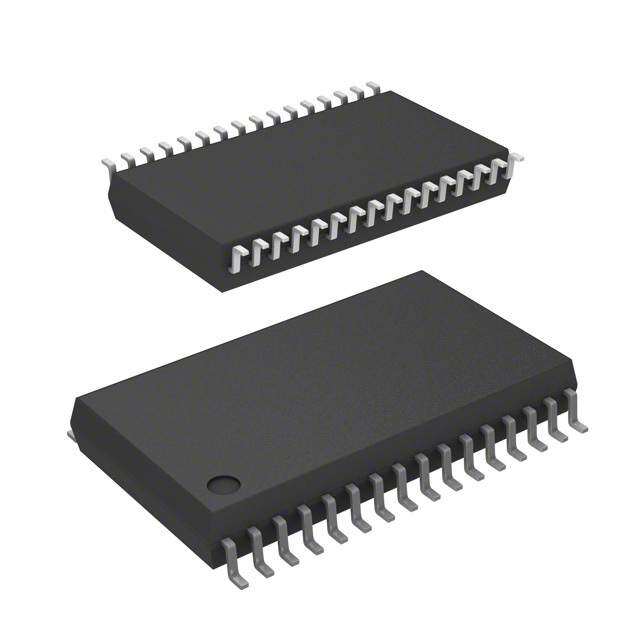
| 封装/外壳 | 8-SOIC(0.154",3.90mm 宽) |
| 封装/箱体 | SOIC-8 |
| 工作温度 | -40°C ~ 85°C |
| 工厂包装数量 | 2500 |
| 最大工作温度 | + 85 C |
| 最小工作温度 | - 40 C |
| 标准包装 | 2,500 |
| 电压-电源 | 4.5 V ~ 52 V |
| 类型 | DC/DC Controller (External Switch) |
| 系列 | TPS40200 |
| 输入电压 | 4.5 V to 52 V |
| 输出数 | 1 |
| 输出电压 | 0.7 V to 46 V |
| 输出端数量 | 1 Output |
| 配用 | /product-detail/zh/TPS40200EVM-001/296-19607-ND/1014182/product-detail/zh/TPS40200EVM-002/296-22911-ND/1671736 |
| 降压 | 是 |
| 隔离式 | 无 |
| 频率-最大值 | 500kHz |


- 商务部:美国ITC正式对集成电路等产品启动337调查
- 曝三星4nm工艺存在良率问题 高通将骁龙8 Gen1或转产台积电
- 太阳诱电将投资9.5亿元在常州建新厂生产MLCC 预计2023年完工
- 英特尔发布欧洲新工厂建设计划 深化IDM 2.0 战略
- 台积电先进制程称霸业界 有大客户加持明年业绩稳了
- 达到5530亿美元!SIA预计今年全球半导体销售额将创下新高
- 英特尔拟将自动驾驶子公司Mobileye上市 估值或超500亿美元
- 三星加码芯片和SET,合并消费电子和移动部门,撤换高东真等 CEO
- 三星电子宣布重大人事变动 还合并消费电子和移动部门
- 海关总署:前11个月进口集成电路产品价值2.52万亿元 增长14.8%


PDF Datasheet 数据手册内容提取
Product Sample & Technical Tools & Support & Folder Buy Documents Software Community TPS40200 SLUS659G–FEBRUARY2006–REVISEDNOVEMBER2014 TPS40200 Wide Input Range Non-Synchronous Voltage Mode Controller 1 Features 3 Description • InputVoltageRange4.5Vto52V The TPS40200 is a flexible, non-synchronous 1 controller with a built-in 200-mA driver for P-channel • OutputVoltage(700mVto90%V ) IN FETs. The circuit operates with inputs up to 52 V with • 200-mAInternalP-channelFETDriver a power-saving feature that turns off driver current • VoltageFeed-ForwardCompensation once the external FET has been fully turned on. This feature extends the flexibility of the device, allowing it • UndervoltageLockout to operate with an input voltage up to 52 V without • ProgrammableFixed-Frequency(between35kHz dissipating excessive power. The circuit operates with and500kHz)Operation voltage-mode feedback and has feed-forward input • ProgrammableShort-CircuitProtection voltage compensation that responds instantly to input voltage change. The integral 700-mV reference is • HiccupOvercurrentFaultRecovery trimmed to 2%, providing the means to accurately • ProgrammableClosed-LoopSoft-Start control low voltages. The TPS40200 is available in an • 700mV1%ReferenceVoltage 8-pin SOIC and an 8-pin VSON package and • ExternalSynchronization supports many of the features of more complex controllers. Clock frequency, soft-start, and • Small8-PinSOIC(D)andVSON(DRB)Packages overcurrent limits are each easily programmed by a single, external component. The part has 2 Applications undervoltage lockout, and can be easily synchronized • IndustrialControl to other controllers or a system clock to satisfy sequencingand/ornoise-reductionrequirements. • DistributedPowerSystems • DSL/CableModems DeviceInformation(1) • Scanners PARTNUMBER PACKAGE BODYSIZE(NOM) • Telecom VSON(8) 3.00mmx3.00mm TPS40200 SOIC(8) 4.90mmx3.90mm (1) For all available packages, see the orderable addendum at theendofthedatasheet. SimplifiedSchematic EfficiencyvsOutputCurrent VIN 100 V =5V OUT 90 TPS40200 1 RC VDD 8 %) 80 ( y c n e 2 SS ISNS 7 Effici 70 V (V) 3 COMP GDRV 6 V IN OUT 16 60 12 8 4 FB GND 5 50 0 0.5 1.0 1.5 2.0 2.5 LoadCurrent(A) UDG-11201 1 An IMPORTANT NOTICE at the end of this data sheet addresses availability, warranty, changes, use in safety-critical applications, intellectualpropertymattersandotherimportantdisclaimers.PRODUCTIONDATA.
TPS40200 SLUS659G–FEBRUARY2006–REVISEDNOVEMBER2014 www.ti.com Table of Contents 1 Features.................................................................. 1 7.4 DeviceFunctionalModes........................................18 2 Applications........................................................... 1 8 ApplicationandImplementation........................ 19 3 Description............................................................. 1 8.1 ApplicationInformation............................................19 4 RevisionHistory..................................................... 2 8.2 TypicalApplication..................................................19 5 PinConfigurationandFunctions......................... 3 9 PowerSupplyRecommendations...................... 37 6 Specifications......................................................... 4 10 Layout................................................................... 37 6.1 AbsoluteMaximumRatings......................................4 10.1 LayoutGuidelines.................................................37 6.2 HandlingRatings......................................................4 10.2 LayoutExample....................................................38 6.3 RecommendedOperatingConditions.......................4 11 DeviceandDocumentationSupport................. 39 6.4 ThermalInformation..................................................4 11.1 DeviceSupport ....................................................39 6.5 ElectricalCharacteristics...........................................5 11.2 DocumentationSupport .......................................39 6.6 TypicalCharacteristics..............................................7 11.3 Trademarks...........................................................39 7 DetailedDescription............................................ 11 11.4 ElectrostaticDischargeCaution............................39 7.1 Overview.................................................................11 11.5 Glossary................................................................39 7.2 FunctionalBlockDiagram.......................................11 12 Mechanical,Packaging,andOrderable Information........................................................... 39 7.3 FeatureDescription.................................................11 4 Revision History ChangesfromRevisionF(September2014)toRevisionG Page • ChangedAddedHandlingRatingtable,FeatureDescriptionsection,DeviceFunctionalModes,Applicationand Implementationsection,PowerSupplyRecommendationssection,Layoutsection,DeviceandDocumentation Supportsection,andMechanical,Packaging,andOrderableInformationsection. .............................................................. 1 2 SubmitDocumentationFeedback Copyright©2006–2014,TexasInstrumentsIncorporated ProductFolderLinks:TPS40200
TPS40200 www.ti.com SLUS659G–FEBRUARY2006–REVISEDNOVEMBER2014 5 Pin Configuration and Functions 8PINS 8PINS VSON(DRB)PACKAGE SOIC(D)PACKAGE (BOTTOMVIEW) (TOPVIEW) RC SS COMP FB RC 1 8 VDD 1 2 3 4 SS 2 7 ISNS COMP 3 6 GDRV FB 4 5 GND 8 7 6 5 VDD ISNS GDRV GND PinFunctions PIN I/O DESCRIPTION NAME NO. COMP 3 O Erroramplifieroutput.ConnectcontrolloopcompensationnetworkfromCOMPtoFB. FB 4 I Erroramplifierinvertinginput.Connectfeedbackresistornetworkcentertaptothispin. GND 5 Deviceground. GDRV 6 O DriveroutputforexternalP-channelMOSFET Current-sensecomparatorinput.ConnectacurrentsenseresistorbetweenISNSandVDDinordertoset ISNS 7 I desiredovercurrentthreshold. SwitchingfrequencysettingRCnetwork.ConnectacapacitorfromtheRCpintotheGNDpinandconnecta resistorfromtheVDDpintotheRCpin.Thedevicemaybesynchronizedtoanexternalclockbyconnecting RC 1 I anopendrainoutputtothispinandpullingittoGND.Formorinfoonpulsewidthforsynchronization, pleaserefertotheSynchronizingtheOscillatorsection. Soft-startprogrammingpin.ConnectcapacitorfromSStoGNDtoprogramsoftstarttime.Pullingthispin SS 2 I below150mVcausestheoutputswitchingtostop,placingthedeviceinashutdownstate.Thepinalso functionsasarestarttimerforovercurrentevents. VDD 8 I Systeminputvoltage.ConnectlocalbypasscapacitorfromVDDtoGND. Copyright©2006–2014,TexasInstrumentsIncorporated SubmitDocumentationFeedback 3 ProductFolderLinks:TPS40200
TPS40200 SLUS659G–FEBRUARY2006–REVISEDNOVEMBER2014 www.ti.com 6 Specifications 6.1 Absolute Maximum Ratings overoperatingfree-airtemperaturerange(unlessotherwisenoted) (1) MIN MAX UNIT V ,ISNS –0.3 52 DD Inputvoltagerange RC,FB –0.3 5.5 V SS –0.3 9.0 COMP –0.3 9.0 Outputvoltagerange V GDRV V –10 V IN IN T OperatingJunctionTemperature –40 125 J °C Leadtemperature1,6mm(1/16inch)fromcasefor10seconds 260 (1) StressesbeyondthoselistedunderAbsoluteMaximumRatingsmaycausepermanentdamagetothedevice.Thesearestressratings only,whichdonotimplyfunctionaloperationofthedeviceattheseoranyotherconditionsbeyondthoseindicatedunderRecommended OperatingConditions.Exposuretoabsolute-maximum-ratedconditionsforextendedperiodsmayaffectdevicereliability. 6.2 Handling Ratings MIN MAX UNIT T Storagetemperaturerange –55 150 °C stg Humanbodymodel(HBM),perANSI/ESDA/JEDECJS-001,all pins(1) –1500 1500 V Electrostaticdischarge V (ESD) Chargeddevicemodel(CDM),perJEDECspecification JESD22-C101,allpins(2) –1500 1500 (1) JEDECdocumentJEP155statesthat500VHBMallowssafemanufacturingwithastandardESDcontrolprocess. (2) JEDECdocumentJEP157statesthat250VCDMallowssafemanufacturingwithastandardESDcontrolprocess. 6.3 Recommended Operating Conditions overoperatingfree-airtemperaturerange(unlessotherwisenoted) MIN MAX UNIT V Inputvoltage 4.5 52 V DD T Operatingtemperaturerange –40 125 °C J 6.4 Thermal Information D DRB THERMALMETRIC(1) SOIC VSON UNIT (8PINS) (8PINS) R Junction-to-ambientthermalresistance 109.6 44.2 θJA R Junction-to-case(top)thermalresistance 54.0 53.6 θJC(top) R Junction-to-boardthermalresistance 49.6 19.8 θJB °C/W ψ Junction-to-topcharacterizationparameter 11.2 1.1 JT ψ Junction-to-boardcharacterizationparameter 49.1 19.9 JB R Junction-to-case(bottom)thermalresistance N/A 7.9 θJC(bot) (1) Formoreinformationabouttraditionalandnewthermalmetrics,seetheICPackageThermalMetricsapplicationreport,SPRA953. 4 SubmitDocumentationFeedback Copyright©2006–2014,TexasInstrumentsIncorporated ProductFolderLinks:TPS40200
TPS40200 www.ti.com SLUS659G–FEBRUARY2006–REVISEDNOVEMBER2014 6.5 Electrical Characteristics –40°C<T =T <85°C,V =12V,f =100kHz(unlessotherwisenoted) A J DD OSC PARAMETER TESTCONDITIONS MIN TYP MAX UNIT VOLTAGEREFERENCE COMP=FB,T =25°C 689 696 702 A T =25°C 686 696 703 A V Feedbackvoltage mV FB 4.5<V <52 –40°C<T <85°C 679 696 708 DD A –40°C<T <125°C 679 696 710 A GATEDRIVER I Gatedriverpull-upcurrent 125 300 mA src I Gatedriverpull-downcurrent 200 300 mA snk V Gatedriveroutputvoltage V =(V –V ),for12<V <52 6 8 10 V GATE GATE DD GDRV DD QUIESCENTCURRENT I Devicequiescentcurrent f =300kHz,Drivernotswitching,4.5<V <52 1.5 3.0 mA qq OSC DD UNDERVOLTAGELOCKOUT(UVLO) V Turn-onthreshold –40°C<T <125°C 3.8 4.25 4.5 UVLO(on) A V V Turn-offthreshold 4.05 UVLO(off) V Hysteresis 110 200 275 mV UVLO(HYST) SOFT-START Internalsoft-startpull-up 65 105 170 R SS(chg) resistance kΩ Internalsoft-startpull-down 190 305 485 R SS(dchg) resistance V Soft-startresetthreshold 100 150 200 mV SSRST OVERCURRENTPROTECTION 0°C<T <125°C 65 100 140 A V Overcurrentthreshold 4.5<V <52 mV ILIM DD –40°C<T <125°C 55 100 140 A OC Overcurrentdutycycle(1) 2% DF V Overcurrentresetthreshold 100 150 200 mV ILIM(rst) OSCILLATOR Oscillatorfrequencyrange(1) 35 500 f R =200kΩ,C =470pF 85 100 115 kHz OSC RC RC Oscillatorfrequency R =68.1kΩ,C =470pF 255 300 345 RC RC 12V<V <52V -9% 0% DD Frequencylineregulation 4.5V<V <12V –20% 0% DD V Rampamplitude 4.5V<V <52V V ÷10 V RMP DD DD (1) Ensuredbydesign.Notproductiontested. Copyright©2006–2014,TexasInstrumentsIncorporated SubmitDocumentationFeedback 5 ProductFolderLinks:TPS40200
TPS40200 SLUS659G–FEBRUARY2006–REVISEDNOVEMBER2014 www.ti.com Electrical Characteristics (continued) –40°C<T =T <85°C,V =12V,f =100kHz(unlessotherwisenoted) A J DD OSC PARAMETER TESTCONDITIONS MIN TYP MAX UNIT PULSEWIDTHMODULATOR Minimumcontrollablepulse VDD=12V 200 400 tMIN width(2) V =30V 100 200 ns DD f =100kHz,C =470pF 93% 95% osc L D Maximumdutycycle MAX f =300kHz,C =470pF 90% 93% osc L K Modulatorandpowerstage 8 10 12 PWM V/V DCgain ERRORAMPLIFIER I Inputbiascurrent 100 250 nA IB AOL Openloopgain(1) 60 80 dB GBWP Unitygainbandwidth(1) 1.5 3 MHz I Outputsourcecurrent V =0.6V,COMP=1V 100 250 μA COMP(src) FB I Outputsinkcurrent V =1.2V,COMP=1V 1.0 2.5 mA COMP(snk) FB (2) SeeFigure21forfort vsf atvariousinputvoltages. MIN OSC 6 SubmitDocumentationFeedback Copyright©2006–2014,TexasInstrumentsIncorporated ProductFolderLinks:TPS40200
TPS40200 www.ti.com SLUS659G–FEBRUARY2006–REVISEDNOVEMBER2014 6.6 Typical Characteristics 1.66 3 1.65 2.5 1.64 1.63 2 1.62 A A I- mDD 1.16.16 I- mDD 1.5 1 1.59 1.58 VDD= 12 V 0.5 1.57 1.56 0 -50 -25 0 25 50 75 100 125 5 10 15 20 25 30 35 40 45 50 55 V - V Temp - °C DD Figure1.QuiescentCurrentvsTemperature Figure2.QuiescentCurrentvsInputVoltage 156.5 4.3 156 4.25 Turn On V m 155.5 V 4.2 d - n - ol O esh 155 urn 4.15 Thr O T et 154.5 VL 4.1 es U R 154 VDD= 12 V 4.05 Turn Off 153.5 4 -50 -25 0 25 50 75 100 125 -50 -25 0 25 50 75 100 125 Temp - °C Temp - °C Figure3.Soft-StartThresholdvsTemperature Figure4.UVLOTurn-OnandTurn-OffvsTemperature 98 103 96 102.5 V = 4.5 V DD 94 102 z) 92 RC == 240720 kpWF mV quency (kH 889680 VDD= 12 V hreshold - 10110.15 VDD= 12 V Fre 84 ItLIM 100.5 100 82 VDD= 52 V 80 99.5 -50 -25 0 25 50 75 100 125 -50 -25 0 25 50 75 100 125 Temp (°C) Temp - °C Figure5.OscillatorFrequencyvsTemperature Figure6.CurrentLimitThresholdvsTemperature Copyright©2006–2014,TexasInstrumentsIncorporated SubmitDocumentationFeedback 7 ProductFolderLinks:TPS40200
TPS40200 SLUS659G–FEBRUARY2006–REVISEDNOVEMBER2014 www.ti.com Typical Characteristics (continued) 275 21.00 270 R = 68.1 kW TJ= 25°C C = 470 pF kHz) 226605 TJ= 25°C 20.50 cy ( 255 n ue 250 dB Freq 245 ain - 20.00 or 240 G at cill 235 19.50 s O 230 225 220 19.00 5 10 15 20 25 30 35 40 45 50 55 5 10 15 20 25 30 35 40 45 50 55 VDD(V) VDD- V Figure7.OscillatorFrequencyvsVDD Figure8.PowerStageGainvsVDD 20.50 20.50 V = 24 V DD 20.30 20.45 V = 4.5 V DD 20.10 20.40 B B d d ain - 19.90 VDD= 12 V ain - 20.35 G G V = 52 V DD 19.70 20.30 19.50 20.25 -50 -25 0 25 50 75 100 125 -50 -25 0 25 50 75 100 125 Temp - °C Temp °C Figure9.PowerStageGainvsTemperature Figure10.PowerStageGainvsTemperature 3 6 5.8 2.8 5.6 2.6 5.4 2.4 VDD= 24 V 5.52 VDD= 52 V 2.2 4.8 V V 4.6 - mp 2 - mp 4.4 Vra 1.8 Vra 4.2 4 1.6 3.8 1.4 V = 12 V 3.6 VDD= 36 V DD 3.4 1.2 3.2 1 3 -50 -25 0 25 50 75 100 125 -50 -25 0 25 50 75 100 125 Temp - °C Temp - °C Figure11.ModulatorRampAmplitudevsTemperature Figure12.ModulatorRampAmplitudevsTemperature 8 SubmitDocumentationFeedback Copyright©2006–2014,TexasInstrumentsIncorporated ProductFolderLinks:TPS40200
TPS40200 www.ti.com SLUS659G–FEBRUARY2006–REVISEDNOVEMBER2014 Typical Characteristics (continued) 6 160 T = 25°C J 140 5 120 4 100 V - A P 3 n 80 VRAM I- IB 60 2 40 1 20 0 0 5 10 15 20 25 30 35 40 45 50 55 -50 -25 0 25 50 75 100 125 V - V DD Temp - °C Figure13.ModulatorRampAmplitudevsVDD Figure14.FeedbackAmplifierInputBiasCurrentvs Temperature 300 3.5 3 250 A A 2.5 m 200 m nt - nt - 2 urre 150 urre C C 1.5 ut ut Outp 100 Outp 1 50 0.5 0 0 -50 -25 0 25 50 75 100 125 -50 -25 0 25 50 75 100 125 Temp - °C Temp - °C Figure15.CompSourceCurrentvsTemperature Figure16.CompSinkCurrentvsTemperature 8 8.4 7.8 VDD= 12V 8.2 VJ= 25°C 7.6 8 V 7.4 - 7.8 E AT 7.2 G V 7.6 7 7.4 6.8 7.2 6.6 6.4 7 -50 -25 0 25 50 75 100 125 5 10 15 20 25 30 35 40 45 50 55 V - V Temp - °C DD Figure17.GateDriveVoltagevsTemperature Figure18.GateDriveVoltagevsVIN Copyright©2006–2014,TexasInstrumentsIncorporated SubmitDocumentationFeedback 9 ProductFolderLinks:TPS40200
TPS40200 SLUS659G–FEBRUARY2006–REVISEDNOVEMBER2014 www.ti.com Typical Characteristics (continued) 720 720 718 718 716 716 714 714 712 712 V V = 24V V - m 710 DD - m 710 B B V = 4.5 V VF708 VF708 DD 706 V = 50 V 706 DD 704 704 V = 12 V DD 702 702 700 700 -50 -25 0 25 50 75 100 125 -50 -25 0 25 50 75 100 125 Temp - °C Temp - °C Figure19.ReferenceVoltagevsTemperature Figure20.ReferenceVoltagevsTemperature 700 100 600 V = 4.5 V 95 DD %) 90 500 ( e dth - ns 400 utyCycl 8850 Pulse Wi 230000 VDD= 24 V VDD= 12 V MaximumD 7705 fOSC (k52H0000z) 100 VDD= 36 V 65 15000 V = 52 V 0 DD 60 0 100 200 300 400 500 0 10 20 30 40 50 Frequency - kHz InputVoltage(V) Figure21.MinimumControllablePulseWidthvsFrequency Figure22.MaximumDutyCyclevsInputVoltage 10 SubmitDocumentationFeedback Copyright©2006–2014,TexasInstrumentsIncorporated ProductFolderLinks:TPS40200
TPS40200 www.ti.com SLUS659G–FEBRUARY2006–REVISEDNOVEMBER2014 7 Detailed Description 7.1 Overview The TPS40200 is a non-synchronous controller with a built in 200-mA driver designed to drive high speed P- channel FETs up to 500 kHz. Small size combined with complete functionality makes the part both versatile and easytouse. The controller uses a low-value current-sensing resistor in series with the input voltage and the power FETs source connection to detect switching current. When the voltage drop across this resistor exceeds 100 mV, the partentersanhiccupfaultmodeatabout2%oftheoperatingfrequency. The device uses voltage feedback to an error amplifier that is biased by a precision 700-mV reference. Feed- forward compensation from the input keeps the PWM gain constant over the full input voltage range, eliminating theneedtochangefrequencycompensationfordifferentinputvoltages. The TPS40200 also incorporates a soft-start feature where the output follows a slowly rising soft-start voltage, preventingoutput-voltageovershoot. 7.2 Functional Block Diagram TPS40200 COMP 3 FB 4 E/AandSS Reference SS 2 + 700mV Soft-Start + 8 VDD and Overcurrent PWM EnableE/A Logic GDRVvoltageswing ISNS 7 limitedto(V –8V) IN Driver 6 GDRV RC 1 OSC 5 GND UVLO UDG-05069 7.3 Feature Description 7.3.1 MOSFETGateDrive Theoutputdriversinkingcurrentisapproximately200mAandisdesignedtodriveP-channelpowerFETs.When the driver pulls the gate charge of the FET it is controlling to 8 V, the drive current folds back to a low level so that high-power dissipation only occurs during the turn-on period of the FET. This feature is particularly valuable when turning on a FET at high input voltages where leaving the gate drive current on would otherwise cause unacceptablepowerdissipation. 7.3.2 UndervoltageLockoutProtection Undervoltage lockout (UVLO) protection ensures proper startup of the device only when the input voltage has exceeded minimum operating voltage. Undervoltage protection incorporates hysteresis which eliminates hiccup startingincaseswhereinputsupplyimpedanceishigh. Copyright©2006–2014,TexasInstrumentsIncorporated SubmitDocumentationFeedback 11 ProductFolderLinks:TPS40200
TPS40200 SLUS659G–FEBRUARY2006–REVISEDNOVEMBER2014 www.ti.com Feature Description (continued) TPS40200 545kW VDD 8 Run + 200kW + 1.3V 36kW GND 5 UDG-05082 Figure23. UndervoltageLockout Undervoltage protection ensures proper startup of the device only when the input voltage has exceeded minimum operating voltage. The UVLO level is measured at the VDD pin with respect to GND. Startup voltage is typically 4.3 V with approximately 200 mV of hysteresis. The device shuts off at a nominal 4.1 V. As shown in Figure 23, when the input V voltage rises to 4.3 V , the 1.3-V comparator’s threshold voltage is exceeded and DD a RUN signal occurs. Feedback from the output closes the switch, and shunts the 200-kΩ resistor so that an approximately200mVlowervoltage,or4.1V,isrequiredbeforethepartshutsdown. 7.3.3 SelectingtheOperatingFrequency TheoperatingfrequencyofthecontrollerisdeterminedbyanexternalresistorR thatisconnectedfromtheRC RC pin to VDD and a capacitor attached from the RC pin to ground. This connection and the two oscillator comparatorsinsidethedevice,areshowninFigure24.TheoscillatorfrequencycanbecalculatedinEquation1. 1 f = SW R ´C ´0.105 RC RC (1) where f istheclockfrequency SW R isthetimingresistorvalueinΩ RC C isthetimingcapacitorvalueinF RC R must be kept large enough that the current through it does not exceed 750 μA when the internal switch RC (showninFigure24)isdischargingthetimingcapacitor.ThisconditionmaybeexpressedbyEquation2. V IN £750mA R RC (2) 7.3.4 SynchronizingtheOscillator Figure 24 shows the functional diagram of the oscillator. When synchronizing the oscillator to an external clock, the RC pin must be pulled below 150 mV for 20 ns or more. The external clock frequency must be higher than the free running frequency of the converter as well. When synchronizing the controller, if the RC pin is held low for an excessive amount of time, erratic operation may occur. The maximum amount of time that the RC pin should be held low is 50% of a nominal output pulse, or 10% of the period of the synchronization frequency whicheverisless. 12 SubmitDocumentationFeedback Copyright©2006–2014,TexasInstrumentsIncorporated ProductFolderLinks:TPS40200
TPS40200 www.ti.com SLUS659G–FEBRUARY2006–REVISEDNOVEMBER2014 Feature Description (continued) Under circumstances where the input voltage is high and the duty cycle is less than 50%, a Schottky diode connected from the RC pin to an external clock may be used to synchronize the oscillator. The cathode of the diode is connected to the RC pin. The trip point of the oscillator is set by an internal voltage divider to be 1/10 of theinputvoltage.Theclocksignalmusthaveanamplitudehigherthanthistrippoint.Whentheclockgoeslow,it allows the reset current to restart the RC ramp, synchronizing the oscillator to the external clock. This provides a simple,single-componentmethodforclocksynchronization. TPS40200 VDD V 8 IN + CLK S Q R RC R Q ExternalFrequency RC Synchronization + (optional) 1 + C 150mV RC GND 5 UDG-05070 Figure24. OscillatorFunctionalDiagram TPS40200 VDD V 8 IN + CLK S Q Amplitude> VIN RRC RC 10 R Q RC + 1 Frequency>ControllerFrequency + C 150mV RC GND 5 UDG-10076 Figure25. Diode-ConnectedSynchronization Copyright©2006–2014,TexasInstrumentsIncorporated SubmitDocumentationFeedback 13 ProductFolderLinks:TPS40200
TPS40200 SLUS659G–FEBRUARY2006–REVISEDNOVEMBER2014 www.ti.com Feature Description (continued) 7.3.5 CurrentLimitResistorSelection As shown in Figure 28, a resistor in series with the power MOSFET sets the overcurrent protection level. Use a low-inductance resistor to avoid ringing signals and nuisance tripping. When the FET is on and the controller senses 100 mV or more drop from the VDD pin to the ISNS pin, an overcurrent condition is declared. When this happens, the FET is turned off, and as shown in Figure 26, the soft-start capacitor is discharged. When the soft- start capacitor reaches a level below 150 mV, the converter clears the overcurrent condition flag and attempts to restart. If the condition that caused the overcurrent event to occur is still present on the output of the converter (see Figure 27), another overcurrent condition is declared and the process repeats indefinitely. Figure 27 shows the soft-start capacitor voltage during an extended output fault condition. The overall duty cycle of current conductionduringapersistentfaultisapproximately2%. V SS TPS40200 100mV + VDD 8 + Fault Latched 100kW 300mV Fault ISNS 7 S Q + SSReference 300kW ErrorAmplifier R Q SS 2 Enable ErrorAmplifier + ResetFault + 150mV GND 5 UDG-10077 Figure26. CurrentLimitReset 14 SubmitDocumentationFeedback Copyright©2006–2014,TexasInstrumentsIncorporated ProductFolderLinks:TPS40200
TPS40200 www.ti.com SLUS659G–FEBRUARY2006–REVISEDNOVEMBER2014 Feature Description (continued) Figure27. TypicalSoft-StartCapacitorandV DuringOvercurrent OUT If necessary, a small RC filter can be added to the current sensing network to reduce nuisance tripping due to noise pickup. This filter can also be used to trim the overcurrent trip point to a higher level with the addition of a single resistor. See Figure 28. The nominal overcurrent trip point using the circuit of Figure 28 is described in Equation3. V R +R I = ILIM ´ F1 F2 OC R R ILIM F2 (3) Where I istheovercurrenttrippoint,peakcurrentintheinductor OC V istheovercurrentthresholdvoltagefortheTPS40200,typically100mV ILIM R isthevalueofthecurrentsenseresistorin Ω ILIM R andR arethevaluesofthescalingresistorsinΩ F1 F2 The value of the capacitor is determined by the nominal pulse width of the converter and the values of the scaling resistors R and R . It is best not to have the time constant of the filter longer than the nominal pulse F1 F2 width of the converter, otherwise a substantial increase in the overcurrent trip point occurs. Using this constraint, thecapacitorvaluemaybeboundedbyEquation4. æ V ö OUT ç ÷ CF £ è(RVIFN1´´RfSFW2)ø (RF1+RF2) (4) Where C isthevalueofthecurrentlimitfiltercapacitorinF F V istheoutputvoltageoftheconverter OUT V istheinputvoltagetotheconverter IN f istheconverterswitchingfrequency SW R andR arethevaluesofthescalingresistorsinΩ F1 F2 Copyright©2006–2014,TexasInstrumentsIncorporated SubmitDocumentationFeedback 15 ProductFolderLinks:TPS40200
TPS40200 SLUS659G–FEBRUARY2006–REVISEDNOVEMBER2014 www.ti.com Feature Description (continued) V IN VDD 8 C F R F2 R ILIM R F1 ISNS 7 GDRV 6 TPS40200 UDG-05071 Figure28. CurrentLimitAdjustment NOTE The current limit resistor and its associated circuitry can be eliminated and the ISNS pin (pin 7) and the VDD pin (pin 8) are shorted. The result of this however, may result in damagetothedeviceorPCboardduringanovercurrentevent. 16 SubmitDocumentationFeedback Copyright©2006–2014,TexasInstrumentsIncorporated ProductFolderLinks:TPS40200
TPS40200 www.ti.com SLUS659G–FEBRUARY2006–REVISEDNOVEMBER2014 Feature Description (continued) 7.3.6 CalculatingtheSoft-StartTime An external capacitor C , connected from the SS pin to ground, controls the soft-start interval. An internal SS charging resistor connected to V produces a rising reference voltage which is connected though a 700-mV DD offset to the reference input of the TPS40200 error amplifier. When the soft-start capacitor voltage (V ) is CSS below 150 mV, there is no switching activity. When V rises above the 700 mV offset, the error amplifier starts CSS to follow V – 700 mV, and uses this rising voltage as a reference. When V reaches 1.4 V, the internal SST CSS reference takes over, and further increases have no effect. An advantage of initiating a slow start in this fashion is that the controller cannot overshoot because its output follows a scaled version of the controller reference voltage. A conceptual drawing of the circuit that produces these results is shown in Figure 29. A consequence of the 700 mV offset is that the controller does not start switching until V has risen to 700 mV. The output CSS remains at 0 V during the resulting delay. When V exceeds the 700 mV offset, the TPS40200 output follows CSS the soft-start time constant. Once above 1.4 V, the 700-mV internal reference takes over, and normal operation begins. VSST TPS40200 700mV Ideal SS 105kW VSST(offset) Diodes 2 + ErrorAmplifier CSS + + FB 700mV 4 COMP 3 UDG-05083 Figure29. Soft-StartCircuit The slow-start time should be longer (slower) than the time constant of the output LC filter. This time constraint maybeexpressedasdescribedinEquation5. t ³2p´ L ´C S OUT OUT (5) The calculation of the soft-start interval is simply the time it takes the RC network to exponentially charge from 0 V to 1.4 V. An internal 105 kΩ charging resistor is connected from the SS pin to V . For applications where the SST voltageisabove8V,aninternalregulatorclampsthemaximumchargingvoltageto8V. Theresultofthisisaformulaforthestart-uptime,asshowninEquation6. æ V ö tSS =RC´CSS´ln´ç SST ÷ V -1.4 è SST ø (6) Where t istherequiredsoft-starttimeinseconds SS C isthesoft-startcapacitorvalueinF SS R istheinternalsoft-startchargingresistor(105kΩ nominal) c V istheinputvoltageuptoamaximumof8V SST Copyright©2006–2014,TexasInstrumentsIncorporated SubmitDocumentationFeedback 17 ProductFolderLinks:TPS40200
TPS40200 SLUS659G–FEBRUARY2006–REVISEDNOVEMBER2014 www.ti.com Feature Description (continued) 7.3.7 VoltageSettingandModulatorGain Since the input current to the error amplifier is negligible, the feedback impedance can be selected over a wide range. Knowing that the reference voltage is 696 mV, choose a convenient value for R1 and then calculate the valueofR2fromEquation7. æ R2ö V =0.696´ 1+ OUT ç ÷ è R1ø (7) V g L V d OUT K PWM C R OUT LOAD V C R2 + V REF R1 UDG-10220 Figure30. SystemGainElements The error amplifier has a DC open loop gain of at least 60 dB with a minimum of a 1.5-MHz gain bandwidth product which gives the user flexibility with respect to the type of feedback compensation he uses for his particular application. The gain selected by the user at the crossover frequency is set to provide an over all unity gain for the system. The crossover frequency should be selected so that the error amplifier open-loop gain is high with respect to the required closed-loop gain, ensuring that the amplifier response is determined by the passivefeedbackelements. 7.4 Device Functional Modes 7.4.1 OperationNearMinimumInputVoltage The TPS40200 is designed to operate with input voltages above 4.5 V. The typical VDD UVLO threshold is 4.25 V and the device may operate at input voltages down to the UVLO voltage. At input voltages below the actual UVLO voltage, the device will not switch. When V passes the UVLO threshold the device will become active. VDD Switching is enabled and the soft start sequence is initiated. The TPS40200 will ramp up the output voltage at theratedeterminedbytheexternalcapacitoratthesoft-startpin. 7.4.2 OperationWithSSPin The SS pin has a 150 mV threshold which can be used to disable the TPS40200. With SS forced below this thresholdvoltagethedeviceisdisabledandswitchingisinhibitedevenifV isaboveitsUVLOthreshold.Ifthe VDD SS voltage is allowed to increase above the threshold while V is above its UVLO threshold, the device VDD becomes active. Switching is enabled and the soft start sequence is initiated. The TPS40200 will ramp up the outputvoltageattheratedeterminedbytheexternalcapacitoratthesoft-startpin. 18 SubmitDocumentationFeedback Copyright©2006–2014,TexasInstrumentsIncorporated ProductFolderLinks:TPS40200
TPS40200 www.ti.com SLUS659G–FEBRUARY2006–REVISEDNOVEMBER2014 8 Application and Implementation NOTE Information in the following applications sections is not part of the TI component specification, and TI does not warrant its accuracy or completeness. TI’s customers are responsible for determining suitability of components for their purposes. Customers should validateandtesttheirdesignimplementationtoconfirmsystemfunctionality. 8.1 Application Information The TPS40200 is a 4.5-V to 52-V buck controller with an integrated gate driver for a high-side p-channel MOSFET. This device is typically used to convert a higher DC voltage to a lower DC voltage with a maximum output current set by an external current sense resistor. In higher current applications, the maximum output current can also be limited by the thermal performance of the external MOSFET and rectifying diode switch. Use thefollowingdesignproceduretoselectexternalcomponentsfortheTPS40200.Thedesignprocedureillustrates thedesignofatypicalbuckregulatorwiththeTPS40200. 8.2 Typical Application 8.2.1 BuckRegulator,8Vto12VInput,3.3Vto5.0Vat2.5-AOutput ThebuckregulatordesignshowninFigure31showstheuseoftheTPS40200.Itdelivers2.5Aateither3.3Vor 5.0Vasselectedbyasinglefeedbackresistor.Itachievesapproximately90%efficiencyat3.3Vand94%at5.0 V. A discussion of design tradeoffs and methodology is included to serve as a guide to the successful design of buckconvertersusingtheTPS40200. The Bill of Materials for this application is given in Table 2. The efficiency and load regulation from boards built fromthisdesignareshowninFigure42andFigure43. + + Notes D3 : Do not populate. SOT 23 Common Cathode Dual Schottky R6 =26.7k for 3.3 Vout, R6 = 16.2k for 5.0 Vout Figure31. 8Vto16V Step-DownBuckConverter IN Copyright©2006–2014,TexasInstrumentsIncorporated SubmitDocumentationFeedback 19 ProductFolderLinks:TPS40200
TPS40200 SLUS659G–FEBRUARY2006–REVISEDNOVEMBER2014 www.ti.com Typical Application (continued) 8.2.1.1 DesignRequirements Table1.DesignParameters PARAMETER TESTCONDITION MIN NOM MAX UNIT V InputVoltage 8 12 16 V IN V OutputVoltage I =2.5A 3.2 3.3 3.4(1) V OUT OUT LineRegulation ±0.2%V 3.293 3.300 3.307 V OUT LoadRegulation ±0.2%V 3.293 3.300 3.307 V OUT V OutputVoltage I at2.5A 4.85 5.0 5.150(1) V OUT OUT LineRegulation ±0.2%×V 4.99 5.00 5.01 V OUT LoadRegulation ±0.2%×V 4.99 5.00 5.01 V OUT V Outputripplevoltage Atmaximumoutputcurrent 60 mV RIPPLE V Outputovershoot For2.5Aloadtransientfrom2.5Ato0.25A 100 mV OVER V Outputundershoot For2.5Aloadtransientfrom0.25Ato2.5A 60 mV UNDER I OutputCurrent 0.125 2.500 A OUT I Shortcircuitcurrenttrippoint 3.75 5.00 A SCP Efficiency Atnominalinputvoltageandmaximumoutput 90% current F Switchingfrequency 300 kHz S (1) Setpointaccuracyisdependentonexternalresistortoleranceandthedevicereferencevoltage.LineandLoadregulationvaluesare referencedtothenominaldesignoutputvoltage. 8.2.1.2 DetailedDesignProcedure 8.2.1.2.1 FETSelectionCriteria • The maximum input voltage for this application is 16 V. Switching the inductor causes overshoot voltages that can equal the input voltage. Since the R of the FET rises with breakdown voltage, select a FET with as DS(on) lowabreakdownvoltageaspossible.Inthiscase,a30-VFETwasselected. • The selection of a power FET size requires knowing both the switching losses and DC losses in the application. AC losses are all frequency dependent and directly related to device capacitances and device size. On the other hand, DC losses are inversely related to device size. The result is an optimum where the two types of losses are equal. Since device size is proportional to R , begin by selecting a device with an DS(on) R that results in a small loss of power relative to package thermal capability and overall efficiency DS(on) objectives. • In this application, the efficiency target is 90% and the output power 8.25 W. This gives a total power-loss budgetof0.916W.TotalFETlossesmustbesmallrelativetothisnumber. TheDCconductionlossintheFETisgivenby:P =I 2×R DC rms DS(on) TheRMScurrentisgivenby: 1 IRMS =æçD´æçIOUT2 +(DIP-P)2 ö÷ö÷2 ç ç 12 ÷÷ ç ÷ è è øø (8) Where t DI =DV´D´ S P-P L I ΔV=V – V –(DCR+R )×I IN OUT DS(on) OUT R istheFETon-stateresistance DS(on) DCRistheinductorDCresistance Disthedutycycle t =thereciprocaloftheswitchingfrequency S 20 SubmitDocumentationFeedback Copyright©2006–2014,TexasInstrumentsIncorporated ProductFolderLinks:TPS40200
TPS40200 www.ti.com SLUS659G–FEBRUARY2006–REVISEDNOVEMBER2014 Usingthevaluesinthisexample,theDCpowerlossis129mW.TheremainingFETlossesareasfollows: • P isthepowerdissipatedwhileswitchingtheFETonandoff SW • P isthepowerdissipateddrivingtheFETgatecapacitance GATE • P isthepowerswitchingtheFEToutputcapacitance COSS ThetotalpowerdissipatedbytheFETisthesumofthesecontributions. P =P +P +P +P FET SW GATE COSS RDS(on) (9) TheP-channelFETusedinthisapplicationisaFDC654Pwiththefollowingcharacteristics: t =13× 10–9 C =83× 10–12 RISE OSS t =6 ×10⁻⁹ Q =9nC FALL G R =0.1Ω V =1.9V DS(on) GATE Q =1.2×10⁻⁹ Q =1.0×10⁻⁹ GD GS UsingthesedevicecharacteristicsandEquation10: f æ ö f ( ) P = S ´çV ´I ´t ÷+ S V ´I ´t =10 mW SW 2 ç IN pk CHON÷ 2 IN pk CHOFF è ø (10) Q ´R Q ´R where tCH(on)= VGD-V G and tCH(off)= GDV G aretheswitchingtimesforthepowerFET. IN TH IN spacer P =Q ×V ×f =22mW (11) GATE G GATE S C ´V 2´f P = OSS IN_MAX S =2 mW CROSS 2 (12) Thegatecurrent,I =Q ×f =2.7mA G G S The sum of the switching losses is 34 mW, and is comparable to the 129-mW DC losses. At added expense, a slightly larger FET is better because the DC loss drops and the AC losses increase, with both moving toward the optimumpointofequallosses. 8.2.1.2.2 RectifierSelectionCriteria 1. RectifierBreakdownVoltage The rectifier has to withstand the maximum input voltage which in this case is 16 V. To allow for switching transientswhichcanapproachtheswitchingvoltagea30-Vrectifierwasselected. 2. DiodeSize The importance of power losses from the Schottky rectifier D2 is determined by the duty cycle. For a low duty cycle application, the rectifier is conducting most of the time, and the current that flows through it times its forward drop can be the largest component of loss in the entire controller. In this application, the duty cycle ranges from 20% to 40%, which in the worst case means that the diode is conducting 80% of the time. Where efficiency is of paramount importance, choose a diode with a minimum of forward drop. In more cost sensitiveapplications,sizemaybereducedtothepointofthethermallimitationsofthediodepackage. The device in this application is large relative to the current required by the application. In a more cost sensitive application, a smaller diode in a less-expensive package will provide a less-efficient but appropriate solution Thedeviceusedhasthefollowingcharacteristics: • V =0.3Vat3A f • C =300pF(C =theeffectivereversevoltagecapacitanceofthesynchronousrectifier,D2). t t ThetwocomponentsofthelossesfromthediodeD2are: Copyright©2006–2014,TexasInstrumentsIncorporated SubmitDocumentationFeedback 21 ProductFolderLinks:TPS40200
TPS40200 SLUS659G–FEBRUARY2006–REVISEDNOVEMBER2014 www.ti.com æ I ö P = V ´çI + RIPPLE ÷´(1-D)=653 mW CON f OUT è 4 ø (13) Where D=thedutycycle I istheripplecurrent RIPPLE I istheoutputcurrent OUT V istheforwardvoltage F P istheconductionpowerloss COND TheswitchingcapacitanceofthisdiodeaddsanACloss,givenby: P = 1éC´(V +V )2´fù =6.8 mW SW 2êë IN f úû (14) Thisadditionallossraisesthetotallossto:660mW. At an output voltage of 3.3 V, the application runs at a nominal duty cycle of 27%, and the diode is conducting 72.5% of the time. As the output voltage is moved up to 5 V, the on-time increases to 46% and the diode is conducting only 54% of the time during each clock cycle. This change in duty cycle proportionately reduces the conductionpowerlossesinthediode.Thisreductionmaybeexpressedas æ0.54ö 660ç ÷= 491mW è0.725ø forasavingsinpowerof660– 491=169mW. To illustrate the relevance of this power savings we measured the full load module Efficiency for this application at 3.3 V and 5 V. The 5-V output efficiency is 92% vs. 89% for the 3.3 V design. This difference in efficiency represents a 456 mW reduction in losses between the two conditions. This 169 mW power-loss reduction in the rectifierrepresents37%ofthedifference. 8.2.1.2.3 InductorSelectionCriteria The P-channel FET driver facilitates switching the power FET at a high frequency. This, in turn, enables the use ofsmaller,less-expensiveinductorsasillustratedinthis300kHzapplication.Ferrite,withitsgoodhighfrequency properties, is the material of choice. Several manufacturers provide catalogs with inductor saturation currents, inductancevalues,andLSRs(internalresistance)fortheirvarious-sizedferrites. In this application, the device must deliver a maximum current of 2.5 A. This requires that the output inductor’s saturation current be above 2.5 A plus ½ the ripple current caused during inductor switching. The value of the inductor determines this ripple current. A low value of inductance has a higher ripple current that contributes to ripple voltage across the resistance of the output capacitors. The advantages of a low inductance are a higher transient response, lower DCR, a higher saturation current, and a smaller, less expensive part. Too low an inductor however, leads to higher peak currents which ultimately are bounded by the overcurrent limit set to protect the output FET or by output ripple voltage. Fortunately, with low ESR Ceramic capacitors on the output, theresultingripplevoltageforrelativelyhighripplecurrentscanbesmall. For example, a single 1-μF, 1206 size, 6.3-V, ceramic capacitor has an internal resistance of 2 Ω at 1 MHz. For this2.5-Aapplication,a10%ripplecurrentof0.25Aproducesa50-mVripplevoltage.Thisripplevoltagemaybe furtherreducedbyadditionalparallelcapacitors. The other bound on inductance is the minimum current at which the controller enters discontinuous conduction. Atthispoint,Inductorcurrentiszero.Theminimumoutputcurrentforthisapplicationisspecifiedat0.125A.This averagecurrentis1/2thepeakcurrentthatmustdevelopduringaminimumontime.Theconditionsforminimum ontimearehighlineandlowload. Using: V -V L = IN OUT ´t =32 mH MIN I on PEAK (15) Where V =16V IN V =3.3V OUT I =0.25A PEAK 22 SubmitDocumentationFeedback Copyright©2006–2014,TexasInstrumentsIncorporated ProductFolderLinks:TPS40200
TPS40200 www.ti.com SLUS659G–FEBRUARY2006–REVISEDNOVEMBER2014 t =0.686μs ON 1 3.3 V t isgivenby ´ ON 300kHz 16 V spacer The inductor used in the circuit is the closest standard value of 33 μH. This is the minimum inductance that can beusedintheconvertertodelivertheminimumcurrentwhilemaintainingcontinuousconduction. 8.2.1.2.4 OutputCapacitance In order to satisfy the output voltage over and under shoot specifications there must be enough output capacitancetokeeptheoutputvoltagewithinthespecifiedvoltagelimitsduringloadcurrentsteps. In a situation where a full load of 2.5 A within the specified voltage limits is suddenly removed, the output capacitor must absorb energy stored in the output inductor. This condition may be described by realizing that the energy in the stored in the inductor must be suddenly absorbed by the output capacitance. This energy relationshipiswrittenas: 1 1 [ ( )] ´L I 2 £ ´ C V 2 -V 2 2 O O 2 O OS O (16) Where V istheallowedover-shootvoltageabovetheoutputvoltage OS L istheinductance O I istheoutputcurrent O C istheoutputcapacitance O V istheoutputvoltage O In this application, the worst case load step is 2.25 A and the allowed overshoot is 100 mV. With a 33 μH output inductor,thisimpliesanoutputcapacitanceof249 μFfora3.3Voutputand165 μFfora5Voutput.. When the load increases from minimum to full load the output capacitor must deliver current to the load. The worst case is for a minimum on time that occurs at 16 V in and 3.3 V and minimum load. This corresponds to OUT an off time of (1 – 0.2 ) times the period 3.3 μs and is the worst case time before the inductor can start supplying current.Thissituationmayberepresentedby: t DV < DI ´ OFFMAX O O C O (17) Where ΔV istheundershootspecificationof60mV O ΔI istheloadcurrentstep O t isthemaximumofftime OFF(max) This condition produces a requirement of 100 μF for the output capacitance. The larger of these two requirementsbecomestheminimumvalueofoutputcapacitance. The ripple current develops a voltage across the ESR of the output capacitance, so another requirement on this componentisitESRbesmallrelativetotheripplevoltagespecification. 8.2.1.2.5 SwitchingFrequency The TPS40200 has a built-in, 8-V, 200-mA, P-channel FET driver output that facilitates using P-channel switching FETs A clock frequency of 300 kHz is chosen as a switching frequency that represents a compromise between a high-frequency that allows the use of smaller capacitors and inductors but one that is not so high as to cause excessive transistor switching losses. As previously discussed, an optimum frequency can be selected bypickingavaluewheretheDCandswitchinglossesareequal. ThefrequencyissetbyusingthedesignformulagivenintheFETSelectionCriteria section. 1 R ´C = RC RC 0.105´f SW (18) Where Copyright©2006–2014,TexasInstrumentsIncorporated SubmitDocumentationFeedback 23 ProductFolderLinks:TPS40200
TPS40200 SLUS659G–FEBRUARY2006–REVISEDNOVEMBER2014 www.ti.com R isthetimingresistorvalueinΩ RC R =68.1kΩ RC C isthetimingcapacitorvalueinF RC C5=470pF f isthedesiredswitchingfrequencyinHz SW f =297kHz. SW At a worst case of 16 V, the timing resistor draws about 250 μA which is well below the 750 μA maximum which thecircuitcanpulldown. 8.2.1.2.6 CalculatingtheOvercurrentThresholdLevel The current limit in the TSP40200 is triggered by a comparator with a 100-mV offset whose inputs are connected across a current-sense resistor between V and the source of the high-side switching FET. When current in this IN resistordevelopsmorethan100mV,thecomparatortripsandterminatestheoutputgatedrive. In this application, the current-limit resistor is set by the peak output stage current which consists of the maximum load current plus ½ the ripple current. In this case, we have 2.5 + 0.125 = 2.625 A. To accommodate tolerances a 25% margin is added giving a 3.25 A peak current. Using the equation below then yields a value for R of0.03 Ω. ILIM Current sensing in a switching environment requires attention to both circuit board traces and noise pick up. In the design shown a small RC filter has been added to the circuit to prevent switching noise from tripping the current sense comparator. The requirements of this filter are board-dependent, but with the layout used in this application,nounreasonableovercurrentisobserved. V IN TPS40200 VDD 8 C F R F2 R ILIM R F1 ISNS 7 GDRV 6 0.1 I = ILIM R ILIM UDG-11200 Figure32. OvercurrentTripCircuitforR Open F2 24 SubmitDocumentationFeedback Copyright©2006–2014,TexasInstrumentsIncorporated ProductFolderLinks:TPS40200
TPS40200 www.ti.com SLUS659G–FEBRUARY2006–REVISEDNOVEMBER2014 8.2.1.2.7 Soft-StartCapacitor Thesoft-startintervalisgiven(inpF)bythefollowingequation: t C = SS ´103 SS æ V ö R´lnç SST ÷ çèVSST-1.4÷ø (19) Where Risaninternal105-kΩ chargingresistor V istheinputvoltageupto8Vwherethechargingvoltageisinternallyclampedto8Vmaximum IN V =700mV,andbecausetheinputvoltageis12V,V =8V. OS SST The oscilloscope picture below shows the expected delay at the output (middle trace) until the soft-start node (bottom trace) reaches 700 mV. At this point, the output rises following the exponential rise of the soft-start capacitor voltage until the soft-start capacitor reaches 1.4 V and the internal 700-mV reference takes over. This total time is approximately 1 ms, which agrees with the calculated value of 0.95 ms where the soft-start capacitanceis0.047 μF. A. Channel1istheoutputvoltage(V )risingto3.3V OUT B. Channel2isthesoftstartpin(SS) Figure33. Soft-StartShowingOutputDelayandControlledRisetoProgrammedOutputVoltage Copyright©2006–2014,TexasInstrumentsIncorporated SubmitDocumentationFeedback 25 ProductFolderLinks:TPS40200
TPS40200 SLUS659G–FEBRUARY2006–REVISEDNOVEMBER2014 www.ti.com 8.2.1.2.8 FrequencyCompensation The four elements that determine the system overall response are discussed below The gain of the error amplifier(K )isthefirstofthereelements.ItsoutputdevelopsacontrolvoltagewhichistheinputtothePWM. EA The TPS40200 has a unique modulator that scales the peak to peak amplitude of the PWM ramp to be 0.1 times the value of the input voltage. Since modulator gain is given by V divided by V , the modulator gain is 10 IN RAMP andisconstantat10(20dB)overtheentirespecifiedinputvoltagerange. The last two elements that affect system gain are the transfer characteristic of the output LC filter and the feedbacknetworkfromtheoutputtotheinputtotheerroramplifier. These four elements maybe expressed by the following expression that represents the system transfer function asshowninFigure34. ( ) TV(S) =KFB ´KEA S ´KPWM ´XLC(S) (20) Where K istheoutputvoltagesettingdivider FB K istheerroramplifierfeedback EA K isthemodulatorgain PWM X isthefiltertransferfunction LC v g v v + c d o V K K X ref EA PWM LC - Tv(s) K FB Figure34. ControlLoop 26 SubmitDocumentationFeedback Copyright©2006–2014,TexasInstrumentsIncorporated ProductFolderLinks:TPS40200
TPS40200 www.ti.com SLUS659G–FEBRUARY2006–REVISEDNOVEMBER2014 Figure 35 shows the feedback network used in this application. This is a Type II compensation network which gives a combination of good transient response and phase boost for good stability. This type of compensation has a pole at the origin causing a –20dB/decade (–1) slope followed by a zero that causes a region of flat gain followed by a final pole that returns the gain slope to –1. The bode plot in Figure 36 shows the effect of these polesandzeros. Theprocedureforsettingupthecompensationnetworkisasfollows: 1. Determinethebreakfrequencyoftheoutputcapacitor. 2. Selectazerofrequencywellbelowthisbreakfrequency. 3. From the gain bandwidth of the error amplifier select a crossover frequency where the amplifier gain is large relativetoexpectedclosedloopgain 4. Selectasecondzerowellabovethecrossoverfrequency,thatreturnsthegainslopetoa –1slope. 5. Calculatetherequiredgainfortheamplifieratcrossover. Bepreparedtoiteratethisproceduretooptimizethepoleandzerolocationsasneeded. The frequency response of this converter is largely determined by two poles that arise from the LC output filter andahigherfrequencyzerocausedbytheESRoftheoutputcapacitance.Thepolesfromtheoutputfiltercause a –40 dB/decade roll off with a phase shift approaching 180 degrees followed by the output capacitor zero that reduced the roll off to –20 dB and gives a phase boost back toward 90 degrees. In other nomenclature, this is a –2 slope followed by a –1 slope. The two zeros in the compensation network act to cancel the double pole from the output filter The compensation network’s two poles produce a region where the error amplifier is flat and can be set to a gain such that the overall gain of the system is zero dB. This region is set so that it brackets the systemcrossoverfrequency. C 7 P1 Slope=–1 C R8 8 dB) n( Z1 P2 ai G R 10 + R 6 V REF f1 f2 Frequency Figure35.ErrorAmplifierFeedbackElements Figure36.ErrorAmplifierBodePlot Copyright©2006–2014,TexasInstrumentsIncorporated SubmitDocumentationFeedback 27 ProductFolderLinks:TPS40200
TPS40200 SLUS659G–FEBRUARY2006–REVISEDNOVEMBER2014 www.ti.com Inordertoproperlycompensatethissystem,itisnecessarytoknowthefrequenciesofitspolesandzeros. 8.2.1.2.8.1 Step1 Thebreakfrequencyoftheoutputcapacitorisgivenby: 1 f = ESR 2p´R ´C ESR OUT (21) Where C =theoutputcapacitor,220μF OUT R =theESRofthecapacitors ESR Because of the ESR of the output capacitor, the output LC filter has a single-pole response above the 1.8-kHz break frequency of the output capacitor and its ESR. This simplifies compensation since the system becomes essentiallyasinglepolesystem. 8.2.1.2.8.2 Step2 The first zero is place well below the 1.8-kHz break frequency of the output capacitor and its ESR. The phase boostfromthiszeroisshowninFigure38. 1 f = Z1 2p´R ´C 8 8 (22) Where R =300kΩ 8 C =1500pF 8 f =354Hz Z1 8.2.1.2.8.3 Step3 From its minimum gain bandwidth product of 1.5 MHz, and knowing it has a 20 dB/decade roll off, the open-loop gain of the error amplifier is 33 dB at 35 kHz. This approximate frequency is chosen for a crossover frequency to keep the amplifier gain contribution to the overall system gain small, as well as following the convention of placingthecrossoverfrequencybetween1/6to1/10the300kHzswitchingfrequency. 8.2.1.2.8.4 Step4 Thesecondpoleisplacedwellabovethe35kHzcrossoverfrequency. 1 f = ´(C +C ) P2 2p´C ´C ´R 7 8 7 8 8 (23) Where R =300kΩ 8 C =10pF 7 C =1500pF 8 f =53kHz P2 28 SubmitDocumentationFeedback Copyright©2006–2014,TexasInstrumentsIncorporated ProductFolderLinks:TPS40200
TPS40200 www.ti.com SLUS659G–FEBRUARY2006–REVISEDNOVEMBER2014 8.2.1.2.8.5 Step5 Calculate the gain elements in the system to determine the gain required by the error amplifier to make the over allgain0dBat35kHz. Thetotalgainaroundthevoltagefeedbackloopis: ( ) TV(S) =KFB ´KEA S ´KPWM ´XLC(S) (24) Where K istheoutputvoltagesettingdivider FB K istheerroramplifierfeedback EA K isthemodulatorgain PWM X isthefiltertransferfunction LC With reference to the graphic below, the output filter's transfer characteristic XLC (S) can be estimated by the following: R L SW VIN D Vsw V OUT 1-D R SR C OUT R LOAD Figure37. OutputFilterAnalysis Z (S) X (S)= OUT LC ( ) Z (S)+Z (S)+R ´D+R ´ 1-D OUT L SW SR (25) Where Z istheparallelcombinationofoutputcapacitor(s)andtheload OUT R istheR oftheswitchingFETplusthecurrent-senseresistor SW DS(on) R istheresistanceofthesynchronousrectifier SR Disthedutycycleestimatedas3.3/12=0.27 ToevaluateX (S)at35kHzusethefollowing: LC • Z (s)at35kHz,whichisdominatedbytheoutputcapacitor'sESR;estimatedtobe400mΩ OUT • Z (s)at35kHzis7.25Ω L • R =0.95mΩ,includingtheR resistance SW LIM • R =100mΩ SR Usingthesenumbers,X (S)=0.04or–27.9dB. LC Thefeedbacknetworkhasagaintotheerroramplifiergivenby: R K = 10 fb R 6 (26) Where for3.3V ,R6=26.7kΩ OUT Usingthevaluesinthisapplication,K =11.4dB. fb Themodulatorhasagainof10thatisflattowellbeyond35kHz,soK =20dB. PWM Toachieve0dboverallgain,theamplifierandfeedbackgainmustbesetto –7.9dB(20dB –27.9dB). Theamplifiergain,includingthefeedbackgain,K ,canbeapproximatedbythisexpression: fb Copyright©2006–2014,TexasInstrumentsIncorporated SubmitDocumentationFeedback 29 ProductFolderLinks:TPS40200
TPS40200 SLUS659G–FEBRUARY2006–REVISEDNOVEMBER2014 www.ti.com V A OUT (S)= VOL V R R IN 1+ 10 + 10 ´(1+A ) R Z VOL 8 FS (27) Where Z istheparallelcombinationofC inparallelwiththesumofR andtheimpedanceofC . fs 7 8 8 A istheopen-loopgainoftheerroramplifierat35kHz,whichis44.6dBor33dB. VOL Figure38showstheresultofthecompensation.Thecrossoverfrequencyis35kHzandthephasemarginis45°. The response of the system is dominated by the ESR of the output capacitor and is exploited to produce an essentiallysingle-polesystemwithsimplecompensation. 50 180 40 Gain 160 Phase 30 140 20 120 10 ain(dB) 0 81000 hase(°) G –10 P 60 –20 –30 40 –40 20 –50 0 0.1 1 10 100 1000 CrossoverFrequency(kHz) Figure38. OverallSystemGainandPhaseResponse Figure38alsoshowsthephaseboostthatgivesthesystemacrossoverphasemarginof47°. The bill of materials for this application is shown below. The efficiency and load regulation from boards built from this design are shown in the following two figures. Gerber PCB layout files and additional application information areavailablefromthefactory. 30 SubmitDocumentationFeedback Copyright©2006–2014,TexasInstrumentsIncorporated ProductFolderLinks:TPS40200
TPS40200 www.ti.com SLUS659G–FEBRUARY2006–REVISEDNOVEMBER2014 Table2.BillofMaterials,BuckRegulator,12Vto3.3Vand5.0V REF.DES. VALUE DESCRIPTION SIZE MFR. PARTNUMBER C1 100μF Capacitor,Aluminum,SM,25V,0.3Ω 8x10mm Sanyo 20SVP100M C12 220μF Capacitor,Aluminum,SM,6.3V,0.4Ω 8x6.2mm Panasonic EEVFC0J221P C13 100pF Capacitor,Ceramic,50V,[COG],[20%] 603 muRata Std. C3 0.1pF Capacitor,Ceramic,50V,[X7R],[20%] 603 muRata Std. C2,C11 1μF Capacitor,Ceramic,50V,[X7R],[20%] 603 muRata Std. C4,C5 470pF Capacitor,Ceramic,50V,[X7R],[20%] 603 muRata Std. C6 0.047μF Capacitor,Ceramic,50V,[X7R],[20%] 603 muRata Std. C7 10pF Capacitor,Ceramic,50V,[COG],[20%] 603 muRata Std. C8 1500pF Capacitor,Ceramic,50V,[X7R],[20%] 603 muRata Std. D1 12V Diode,Zener,12-V,350mW SOT23 Diodes,Inc. BZX84C12T D2 Diode,Schottky,30A,30V SMC OnSemi MBRS330T3 D3 12V DiodeZener12V5mA VMD2 Rohm VDZT2R12B J1,J3 TerminalBlock4-Pin15A5.1mm 0.8x0.35 OST ED2227 J2 Header,2-pin,100milspacing,(36-pinstrip) 0.100x2 Sullins PTC36SAAN L1 33μH Inductor,SMT,3.2A,.039Ω 12.5x12.5mm TDK SLF12575T330M3R2PF PCB 2LayerPCB2OunceCu 1.4x2.12x0.062 HPA164 Q1 Trans,N-ChanEnhancementSwitching,50mA SOT-143B Phillips BSS83 Q2 MOSFET,P-ch,30V,3.6A,75mΩ SuperSOT-6 Fairchild FDC654P U1 IC,LowCostNon-SyncBuckController SO-8 TI TPS40200D R1 10Ω Resistor,Chip,1/16W,1% 603 Std. Std. R10 100kΩ Resistor,Chip,,1/16W,1% 603 Std. Std. R11 10kΩ Resistor,Chip,1/16W,1% 603 Std. Std. R12 1MΩ Resistor,Chip,1/16W,1% 603 Std. Std. R13 49.9Ω Resistor,Chip,1/16W,1% 603 Std. Std. R2 0.02Ω Resistor,Chip,½W,5% 2010 Std. Std. R3 68.1kΩ Resistor,Chip,1/16W,1% 603 Std. Std. R4 2.0kΩ Resistor,Chip,1/16W,1% 603 Std. Std. R5 0Ω Resistor,Chip,1/16W,1% 603 Std. Std. R6 26.7kΩ Resistor,Chip,1/16W,1% 603 Std. Std. R7 1.0kΩ Resistor,Chip,1/16W,1% 603 Std. Std. R8 300kΩ Resistor,Chip,1/16W,1% 603 Std. Std. 8.2.1.2.9 PrintedCircuitBoardPlots The following figures Figure 39 through Figure 41 show the design of the TPS40200EVM-001 printed circuit board. The design uses 2-layer, 2-oz copper and is 1.4” x 2.3” in size. All components are mounted on the top side to allow the user to easily view, probe, and evaluate the TPS40200 control IC in a practical application. Moving components to both sides of the printed circuit board (PCB) or using additional internal layers can offer additionalsizereductionforspaceconstrainedapplications. Copyright©2006–2014,TexasInstrumentsIncorporated SubmitDocumentationFeedback 31 ProductFolderLinks:TPS40200
TPS40200 SLUS659G–FEBRUARY2006–REVISEDNOVEMBER2014 www.ti.com Figure39. TPS40200EVM-001ComponentPlacement(ViewedfromTop) Figure40. TPS40200EVM-001TopCopper(ViewedfromTop) Figure41. TPS40200EVM-001BottomCopper(X-RayViewfromTop) 32 SubmitDocumentationFeedback Copyright©2006–2014,TexasInstrumentsIncorporated ProductFolderLinks:TPS40200
TPS40200 www.ti.com SLUS659G–FEBRUARY2006–REVISEDNOVEMBER2014 8.2.1.3 ApplicationCurves 100 100 V =5V OUT VOUT=3.3V 90 90 %) 80 %) 80 ( ( y y c c n n e e Effici 70 Effici 70 VIN(V) VIN(V) 16 16 60 60 12 12 8 8 50 50 0 0.5 1.0 1.5 2.0 2.5 0 0.5 1.0 1.5 2.0 2.5 LoadCurrent(A) LoadCurrent(A) Figure42.Full-LoadEfficiencyat5.0V Figure43.Full-LoadEfficiencyat3.3V OUT OUT 8.2.2 18V-50VInput,16Vat1-AOutput This is an example of using the TPS40200 in a higher voltage application. The output voltage is 16 V at 1 A with an18Vto50Vinput.Someofthetestresultsareshownbelow. + + Figure44. BuckConverter.V =18Vto50V;V =16V@1A IN OUT Copyright©2006–2014,TexasInstrumentsIncorporated SubmitDocumentationFeedback 33 ProductFolderLinks:TPS40200
TPS40200 SLUS659G–FEBRUARY2006–REVISEDNOVEMBER2014 www.ti.com 8.2.2.1 DesignRequirements Table3.DesignParameters PARAMETER MIN NOM MAX UNIT V InputVoltage 18 50 IN V V OutputVoltage 16 OUT I OutputCurrent 1 OUT A I Shortcircuitcurrenttrippoint 2 SCP F SwitchingFrequency 200 kHz S 8.2.2.2 DetailedDesignProcedures Using the design parameters stated in Table 3, follow the detailed design procedures listed under Detailed DesignProcedure. 8.2.2.3 ApplicationCurves 100 16.50 16.45 95 16.40 90 V) %) e( 16.35 ency( 85 Voltag 16.30 Effici 80 utput 16.25 O VIN(V) 16.20 VIN(V) 75 24 24 16.15 48 48 70 16.10 0.1 0.2 0.3 0.4 0.5 0.6 0.7 0.8 0.9 1.0 0.0 0.1 0.2 0.3 0.4 0.5 0.6 0.7 0.8 0.9 1.0 LoadCurrent(A) LoadCurrent (A) Figure45.Efficiencyvs.Load Figure46.17604LoadRegulation,TwoInputVoltage Extremes 34 SubmitDocumentationFeedback Copyright©2006–2014,TexasInstrumentsIncorporated ProductFolderLinks:TPS40200
TPS40200 www.ti.com SLUS659G–FEBRUARY2006–REVISEDNOVEMBER2014 8.2.3 WideInputVoltageLedConstantCurrentDriver This application uses the TPS40200 as a buck controller that drives a string of LED diodes. The feedback point for this circuit is a sense resistor in series with this string. The low 0.7 V reference minimizes power wasted in this resistor, and maintains the LED current at a value given by 0.7/R . As the input voltage is varied, the SENSE duty cycle changes to maintain the LED current at a constant value so that the light intensity does not change withlargeinputvoltagevariations. + + Figure47. Wide-InputVoltageRangeLEDDriver 8.2.3.1 DesignRequirements Table4.DesignParameters PARAMETER MIN NOM MAX UNIT V InputVoltage 12 30 V IN I OutputVoltage 0.25 AA LED I Shortcircuitcurrenttrippoint 3.3 A SCP F SwitchingFrequency 300 kHz S Copyright©2006–2014,TexasInstrumentsIncorporated SubmitDocumentationFeedback 35 ProductFolderLinks:TPS40200
TPS40200 SLUS659G–FEBRUARY2006–REVISEDNOVEMBER2014 www.ti.com 8.2.3.2 DetailedDesignProcedures Using the design parameters stated in Table 4, follow the detailed design procedures listed under Detailed DesignProcedure. 8.2.3.3 ApplicationCurve 100 90 %) 80 ( y c n e Effici 70 60 50 10 15 20 25 30 InputVoltage(V) Figure48.EfficiencyvsInputVoltage 36 SubmitDocumentationFeedback Copyright©2006–2014,TexasInstrumentsIncorporated ProductFolderLinks:TPS40200
TPS40200 www.ti.com SLUS659G–FEBRUARY2006–REVISEDNOVEMBER2014 9 Power Supply Recommendations The TPS40200 is designed to operate from an input voltage supply range between 4.5 V and 52 V. This input supply should be well regulated. If the input supply is located more than a few inches from the buck power stage controlled by the TPS40200, additional bulk capacitance may be required in addition to the ceramic-bypass capacitors.Anelectrolyticcapacitorwithavalueof100uFisatypicalchoice. 10 Layout 10.1 Layout Guidelines • Keep the AC current loops as short as possible. For the maximum effectiveness from C3, place it near the VDD pin of the controller and design the input AC loop consisting of C1-R -Q1-D1 to be as short as SENSE possible. Excessive high frequency noise on VDD during switching degrades overall regulation as the load increases. • Keep the output loop A (D1-L1-C2) as small as possible. A larger loop can degrade the application output noiseperformance. • Traces carrying large AC currents should NOT be connected through a ground plane. Instead, use PCB tracesonthetoplayertoconducttheACcurrentandusethegroundplaneasanoiseshield.Splittheground plane as necessary to keep noise away from the TPS40200 and noise sensitive areas such as feedback resistorsR6,andR10. • Keep the SW node as physically small as possible to minimize parasitic capacitance and to minimize radiated emissions. • Forgoodoutputvoltageregulation,KelvinconnectionsshouldbebroughtfromtheloadtoR6andR10. • The trace from the R6-R10 junction to the TPS40200 should be short and kept away from any noise source (suchastheSWnode). • ThegatedrivetraceshouldbeascloseaspossibletothepowerFETgate. Copyright©2006–2014,TexasInstrumentsIncorporated SubmitDocumentationFeedback 37 ProductFolderLinks:TPS40200
TPS40200 SLUS659G–FEBRUARY2006–REVISEDNOVEMBER2014 www.ti.com 10.2 Layout Example R3 R1 Input C5 C3 C6 TPS40200 RSENSE C1 1 RC VDD 8 C4 Q1 R5 L1 2 SS ISNS 7 Output R4 C2 3 COMP GDRV 6 D1 C7 C8 Ground 4 FB GND 5 R8 R9 C9 R6 R10 UDG-07045 Input C5 R3 C3 R1 C6 RC TPS40200 VDD C4 R4 SS ISEN RSENSE C1 R5 COMP GDRV Highcurrent Powerstagecomponents FB GND 8 7 Q1 C C Switchnode L1 Output R8 R6 LowcurrentControl R9 D1 C2 Components R10 9 Ground C KelvinGround KelvinVoltage Sense Figure49. PCBoardLayoutRecommendations 38 SubmitDocumentationFeedback Copyright©2006–2014,TexasInstrumentsIncorporated ProductFolderLinks:TPS40200
TPS40200 www.ti.com SLUS659G–FEBRUARY2006–REVISEDNOVEMBER2014 11 Device and Documentation Support 11.1 Device Support 11.1.1 RelatedProducts DEVICENUMBER DESCRIPTION TPS4007 LowInputSynchronousBuckController TPS4009 TL5001 WideInputRangeController TPS40057 Wideinput(8Vto40V)SynchronousBuckController TPS40190 LowPinCountSynchronousBuckController TPS40192 –4.5Vto18VLowPinCountSynchronousBuckController TPS40193 11.1.2 Third-PartyProductsDisclaimer TI'S PUBLICATION OF INFORMATION REGARDING THIRD-PARTY PRODUCTS OR SERVICES DOES NOT CONSTITUTE AN ENDORSEMENT REGARDING THE SUITABILITY OF SUCH PRODUCTS OR SERVICES OR A WARRANTY, REPRESENTATION OR ENDORSEMENT OF SUCH PRODUCTS OR SERVICES, EITHER ALONEORINCOMBINATIONWITHANYTIPRODUCTORSERVICE. 11.2 Documentation Support 11.2.1 RelatedDocumentation • UndertheHoodofLowVoltageDC/DCConverters–SEM1500Topic5 – 2002SeminarSeries • UnderstandingBuckPowerStagesinSwitchmodePowerSupplies –SLVA057 • Design and Application Guide for High Speed MOSFET Gate Drive Circuits- SEM 1400 – 2001 Seminar Series • DesigningStableControlLoops-SEM1400– 2001SeminarSeries • http://power.ti.com 11.3 Trademarks Alltrademarksarethepropertyoftheirrespectiveowners. 11.4 Electrostatic Discharge Caution Thesedeviceshavelimitedbuilt-inESDprotection.Theleadsshouldbeshortedtogetherorthedeviceplacedinconductivefoam duringstorageorhandlingtopreventelectrostaticdamagetotheMOSgates. 11.5 Glossary SLYZ022—TIGlossary. Thisglossarylistsandexplainsterms,acronyms,anddefinitions. 12 Mechanical, Packaging, and Orderable Information The following pages include mechanical, packaging, and orderable information. This information is the most current data available for the designated devices. This data is subject to change without notice and revision of thisdocument.Forbrowser-basedversionsofthisdatasheet,refertotheleft-handnavigation. Copyright©2006–2014,TexasInstrumentsIncorporated SubmitDocumentationFeedback 39 ProductFolderLinks:TPS40200
PACKAGE OPTION ADDENDUM www.ti.com 11-Sep-2014 PACKAGING INFORMATION Orderable Device Status Package Type Package Pins Package Eco Plan Lead/Ball Finish MSL Peak Temp Op Temp (°C) Device Marking Samples (1) Drawing Qty (2) (6) (3) (4/5) TPS40200D ACTIVE SOIC D 8 75 Green (RoHS CU NIPDAU Level-1-260C-UNLIM -40 to 85 40200 & no Sb/Br) TPS40200DG4 ACTIVE SOIC D 8 75 Green (RoHS CU NIPDAU Level-1-260C-UNLIM -40 to 85 40200 & no Sb/Br) TPS40200DR ACTIVE SOIC D 8 2500 Green (RoHS CU NIPDAU Level-1-260C-UNLIM -40 to 85 40200 & no Sb/Br) TPS40200DRBR ACTIVE SON DRB 8 3000 Green (RoHS CU NIPDAU Level-2-260C-1 YEAR -40 to 85 4200 & no Sb/Br) TPS40200DRBT ACTIVE SON DRB 8 250 Green (RoHS CU NIPDAU Level-2-260C-1 YEAR -40 to 85 4200 & no Sb/Br) TPS40200DRG4 ACTIVE SOIC D 8 2500 Green (RoHS CU NIPDAU Level-1-260C-UNLIM -40 to 85 40200 & no Sb/Br) TPS40200GDR ACTIVE SOIC D 8 2500 Green (RoHS CU NIPDAU Level-1-260C-UNLIM -40 to 85 40200 & no Sb/Br) (1) The marketing status values are defined as follows: ACTIVE: Product device recommended for new designs. LIFEBUY: TI has announced that the device will be discontinued, and a lifetime-buy period is in effect. NRND: Not recommended for new designs. Device is in production to support existing customers, but TI does not recommend using this part in a new design. PREVIEW: Device has been announced but is not in production. Samples may or may not be available. OBSOLETE: TI has discontinued the production of the device. (2) Eco Plan - The planned eco-friendly classification: Pb-Free (RoHS), Pb-Free (RoHS Exempt), or Green (RoHS & no Sb/Br) - please check http://www.ti.com/productcontent for the latest availability information and additional product content details. TBD: The Pb-Free/Green conversion plan has not been defined. Pb-Free (RoHS): TI's terms "Lead-Free" or "Pb-Free" mean semiconductor products that are compatible with the current RoHS requirements for all 6 substances, including the requirement that lead not exceed 0.1% by weight in homogeneous materials. Where designed to be soldered at high temperatures, TI Pb-Free products are suitable for use in specified lead-free processes. Pb-Free (RoHS Exempt): This component has a RoHS exemption for either 1) lead-based flip-chip solder bumps used between the die and package, or 2) lead-based die adhesive used between the die and leadframe. The component is otherwise considered Pb-Free (RoHS compatible) as defined above. Green (RoHS & no Sb/Br): TI defines "Green" to mean Pb-Free (RoHS compatible), and free of Bromine (Br) and Antimony (Sb) based flame retardants (Br or Sb do not exceed 0.1% by weight in homogeneous material) (3) MSL, Peak Temp. - The Moisture Sensitivity Level rating according to the JEDEC industry standard classifications, and peak solder temperature. (4) There may be additional marking, which relates to the logo, the lot trace code information, or the environmental category on the device. Addendum-Page 1
PACKAGE OPTION ADDENDUM www.ti.com 11-Sep-2014 (5) Multiple Device Markings will be inside parentheses. Only one Device Marking contained in parentheses and separated by a "~" will appear on a device. If a line is indented then it is a continuation of the previous line and the two combined represent the entire Device Marking for that device. (6) Lead/Ball Finish - Orderable Devices may have multiple material finish options. Finish options are separated by a vertical ruled line. Lead/Ball Finish values may wrap to two lines if the finish value exceeds the maximum column width. Important Information and Disclaimer:The information provided on this page represents TI's knowledge and belief as of the date that it is provided. TI bases its knowledge and belief on information provided by third parties, and makes no representation or warranty as to the accuracy of such information. Efforts are underway to better integrate information from third parties. TI has taken and continues to take reasonable steps to provide representative and accurate information but may not have conducted destructive testing or chemical analysis on incoming materials and chemicals. TI and TI suppliers consider certain information to be proprietary, and thus CAS numbers and other limited information may not be available for release. In no event shall TI's liability arising out of such information exceed the total purchase price of the TI part(s) at issue in this document sold by TI to Customer on an annual basis. OTHER QUALIFIED VERSIONS OF TPS40200 : •Automotive: TPS40200-Q1 •Enhanced Product: TPS40200-EP NOTE: Qualified Version Definitions: •Automotive - Q100 devices qualified for high-reliability automotive applications targeting zero defects •Enhanced Product - Supports Defense, Aerospace and Medical Applications Addendum-Page 2
PACKAGE MATERIALS INFORMATION www.ti.com 11-Sep-2014 TAPE AND REEL INFORMATION *Alldimensionsarenominal Device Package Package Pins SPQ Reel Reel A0 B0 K0 P1 W Pin1 Type Drawing Diameter Width (mm) (mm) (mm) (mm) (mm) Quadrant (mm) W1(mm) TPS40200DR SOIC D 8 2500 330.0 12.4 6.4 5.2 2.1 8.0 12.0 Q1 TPS40200DRBR SON DRB 8 3000 330.0 12.4 3.3 3.3 1.1 8.0 12.0 Q2 TPS40200DRBT SON DRB 8 250 180.0 12.4 3.3 3.3 1.1 8.0 12.0 Q2 TPS40200GDR SOIC D 8 2500 330.0 12.4 6.4 5.2 2.1 8.0 12.0 Q1 PackMaterials-Page1
PACKAGE MATERIALS INFORMATION www.ti.com 11-Sep-2014 *Alldimensionsarenominal Device PackageType PackageDrawing Pins SPQ Length(mm) Width(mm) Height(mm) TPS40200DR SOIC D 8 2500 340.5 338.1 20.6 TPS40200DRBR SON DRB 8 3000 367.0 367.0 35.0 TPS40200DRBT SON DRB 8 250 210.0 185.0 35.0 TPS40200GDR SOIC D 8 2500 340.5 338.1 20.6 PackMaterials-Page2
PACKAGE OUTLINE D0008A SOIC - 1.75 mm max height SCALE 2.800 SMALL OUTLINE INTEGRATED CIRCUIT C SEATING PLANE .228-.244 TYP [5.80-6.19] .004 [0.1] C A PIN 1 ID AREA 6X .050 [1.27] 8 1 2X .189-.197 [4.81-5.00] .150 NOTE 3 [3.81] 4X (0 -15 ) 4 5 8X .012-.020 B .150-.157 [0.31-0.51] .069 MAX [3.81-3.98] .010 [0.25] C A B [1.75] NOTE 4 .005-.010 TYP [0.13-0.25] 4X (0 -15 ) SEE DETAIL A .010 [0.25] .004-.010 0 - 8 [0.11-0.25] .016-.050 [0.41-1.27] DETAIL A (.041) TYPICAL [1.04] 4214825/C 02/2019 NOTES: 1. Linear dimensions are in inches [millimeters]. Dimensions in parenthesis are for reference only. Controlling dimensions are in inches. Dimensioning and tolerancing per ASME Y14.5M. 2. This drawing is subject to change without notice. 3. This dimension does not include mold flash, protrusions, or gate burrs. Mold flash, protrusions, or gate burrs shall not exceed .006 [0.15] per side. 4. This dimension does not include interlead flash. 5. Reference JEDEC registration MS-012, variation AA. www.ti.com
EXAMPLE BOARD LAYOUT D0008A SOIC - 1.75 mm max height SMALL OUTLINE INTEGRATED CIRCUIT 8X (.061 ) [1.55] SYMM SEE DETAILS 1 8 8X (.024) [0.6] SYMM (R.002 ) TYP [0.05] 5 4 6X (.050 ) [1.27] (.213) [5.4] LAND PATTERN EXAMPLE EXPOSED METAL SHOWN SCALE:8X SOLDER MASK SOLDER MASK METAL OPENING OPENING METAL UNDER SOLDER MASK EXPOSED METAL EXPOSED METAL .0028 MAX .0028 MIN [0.07] [0.07] ALL AROUND ALL AROUND NON SOLDER MASK SOLDER MASK DEFINED DEFINED SOLDER MASK DETAILS 4214825/C 02/2019 NOTES: (continued) 6. Publication IPC-7351 may have alternate designs. 7. Solder mask tolerances between and around signal pads can vary based on board fabrication site. www.ti.com
EXAMPLE STENCIL DESIGN D0008A SOIC - 1.75 mm max height SMALL OUTLINE INTEGRATED CIRCUIT 8X (.061 ) [1.55] SYMM 1 8 8X (.024) [0.6] SYMM (R.002 ) TYP [0.05] 5 4 6X (.050 ) [1.27] (.213) [5.4] SOLDER PASTE EXAMPLE BASED ON .005 INCH [0.125 MM] THICK STENCIL SCALE:8X 4214825/C 02/2019 NOTES: (continued) 8. Laser cutting apertures with trapezoidal walls and rounded corners may offer better paste release. IPC-7525 may have alternate design recommendations. 9. Board assembly site may have different recommendations for stencil design. www.ti.com
None
PACKAGE OUTLINE DRB0008B VSON - 1 mm max height SCALE 4.000 PLASTIC SMALL OUTLINE - NO LEAD 3.1 B A 2.9 PIN 1 INDEX AREA 3.1 2.9 C 1 MAX SEATING PLANE 0.05 0.08 C 0.00 EXPOSED 1.65 0.05 (0.2) TYP THERMAL PAD 4 5 2X 1.95 2.4 0.05 8 1 6X 0.65 0.35 8X 0.25 PIN 1 ID 0.5 0.1 C A B (OPTIONAL) 8X 0.3 0.05 C 4218876/A 12/2017 NOTES: 1. All linear dimensions are in millimeters. Any dimensions in parenthesis are for reference only. Dimensioning and tolerancing per ASME Y14.5M. 2. This drawing is subject to change without notice. 3. The package thermal pad must be soldered to the printed circuit board for thermal and mechanical performance. www.ti.com
EXAMPLE BOARD LAYOUT DRB0008B VSON - 1 mm max height PLASTIC SMALL OUTLINE - NO LEAD (1.65) 8X (0.6) SYMM 1 8 8X (0.3) (2.4) (0.95) 6X (0.65) 4 5 (R0.05) TYP (0.575) ( 0.2) VIA (2.8) TYP LAND PATTERN EXAMPLE SCALE:20X 0.07 MAX 0.07 MIN ALL AROUND ALL AROUND SOLDER MASK METAL METAL UNDER SOLDER MASK OPENING SOLDER MASK OPENING NON SOLDER MASK SOLDER MASK DEFINED DEFINED (PREFERRED) SOLDER MASK DETAILS 4218876/A 12/2017 NOTES: (continued) 4. This package is designed to be soldered to a thermal pad on the board. For more information, see Texas Instruments literature number SLUA271 (www.ti.com/lit/slua271). 5. Vias are optional depending on application, refer to device data sheet. If any vias are implemented, refer to their locations shown on this view. It is recommended that vias under paste be filled, plugged or tented. www.ti.com
EXAMPLE STENCIL DESIGN DRB0008B VSON - 1 mm max height PLASTIC SMALL OUTLINE - NO LEAD SYMM 8X (0.6) METAL TYP 1 8X (0.3) 8 (0.63) SYMM 6X (0.65) (1.06) 5 4 (R0.05) TYP (1.47) (2.8) SOLDER PASTE EXAMPLE BASED ON 0.125 mm THICK STENCIL EXPOSED PAD 81% PRINTED SOLDER COVERAGE BY AREA SCALE:25X 4218876/A 12/2017 NOTES: (continued) 6. Laser cutting apertures with trapezoidal walls and rounded corners may offer better paste release. IPC-7525 may have alternate design recommendations. www.ti.com
IMPORTANTNOTICEANDDISCLAIMER TIPROVIDESTECHNICALANDRELIABILITYDATA(INCLUDINGDATASHEETS),DESIGNRESOURCES(INCLUDINGREFERENCE DESIGNS),APPLICATIONOROTHERDESIGNADVICE,WEBTOOLS,SAFETYINFORMATION,ANDOTHERRESOURCES“ASIS” ANDWITHALLFAULTS,ANDDISCLAIMSALLWARRANTIES,EXPRESSANDIMPLIED,INCLUDINGWITHOUTLIMITATIONANY IMPLIEDWARRANTIESOFMERCHANTABILITY,FITNESSFORAPARTICULARPURPOSEORNON-INFRINGEMENTOFTHIRD PARTYINTELLECTUALPROPERTYRIGHTS. TheseresourcesareintendedforskilleddevelopersdesigningwithTIproducts.Youaresolelyresponsiblefor(1)selectingtheappropriate TIproductsforyourapplication,(2)designing,validatingandtestingyourapplication,and(3)ensuringyourapplicationmeetsapplicable standards,andanyothersafety,security,orotherrequirements.Theseresourcesaresubjecttochangewithoutnotice.TIgrantsyou permissiontousetheseresourcesonlyfordevelopmentofanapplicationthatusestheTIproductsdescribedintheresource.Other reproductionanddisplayoftheseresourcesisprohibited.NolicenseisgrantedtoanyotherTIintellectualpropertyrightortoanythird partyintellectualpropertyright.TIdisclaimsresponsibilityfor,andyouwillfullyindemnifyTIanditsrepresentativesagainst,anyclaims, damages,costs,losses,andliabilitiesarisingoutofyouruseoftheseresources. TI’sproductsareprovidedsubjecttoTI’sTermsofSale(www.ti.com/legal/termsofsale.html)orotherapplicabletermsavailableeitheron ti.comorprovidedinconjunctionwithsuchTIproducts.TI’sprovisionoftheseresourcesdoesnotexpandorotherwisealterTI’sapplicable warrantiesorwarrantydisclaimersforTIproducts. MailingAddress:TexasInstruments,PostOfficeBox655303,Dallas,Texas75265 Copyright©2019,TexasInstrumentsIncorporated