ICGOO在线商城 > TPS40055EVM-001
 Datasheet下载
- 型号: TPS40055EVM-001
- 制造商: Texas Instruments
- 库位|库存: xxxx|xxxx
- 要求:
| 数量阶梯 | 香港交货 | 国内含税 |
| +xxxx | $xxxx | ¥xxxx |
查看当月历史价格
查看今年历史价格
TPS40055EVM-001产品简介:
ICGOO电子元器件商城为您提供TPS40055EVM-001由Texas Instruments设计生产,在icgoo商城现货销售,并且可以通过原厂、代理商等渠道进行代购。 提供TPS40055EVM-001价格参考¥371.66-¥371.66以及Texas InstrumentsTPS40055EVM-001封装/规格参数等产品信息。 你可以下载TPS40055EVM-001参考资料、Datasheet数据手册功能说明书, 资料中有TPS40055EVM-001详细功能的应用电路图电压和使用方法及教程。
| 参数 | 数值 |
| 产品目录 | 编程器,开发系统半导体 |
| 描述 | EVAL MODULE FOR TPS40055-001电源管理IC开发工具 Eval Mod Converter |
| 产品分类 | |
| 品牌 | Texas Instruments |
| 产品手册 | http://www.ti.com/lit/pdf/sluu186 |
| 产品图片 | |
| rohs | 否无铅 / 符合限制有害物质指令(RoHS)规范要求 |
| 产品系列 | 电源管理IC开发工具,Texas Instruments TPS40055EVM-001- |
| 数据手册 | 点击此处下载产品Datasheethttp://www.ti.com/lit/pdf/sluu186 |
| 产品型号 | TPS40055EVM-001 |
| 主要用途 | DC/DC,步降 |
| 产品 | Evaluation Boards |
| 产品目录页面 | |
| 产品种类 | 电源管理IC开发工具 |
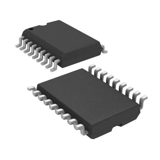
| 使用的IC/零件 | TPS40055 |
| 其它名称 | 296-18953 |
| 制造商产品页 | http://www.ti.com/general/docs/suppproductinfo.tsp?distId=10&orderablePartNumber=TPS40055EVM-001 |
| 功率-输出 | - |
| 商标 | Texas Instruments |
| 尺寸 | 72.4 mm x 50.8 mm |
| 工具用于评估 | TPS40055 |
| 工厂包装数量 | 1 |
| 所含物品 | 板 |
| 板类型 | 完全填充 |
| 标准包装 | 1 |
| 电压-输入 | 10 V ~ 14 V |
| 电压-输出 | 1.8V |
| 电流-输出 | 15A |
| 相关产品 | /product-detail/zh/TPS40055PWPRG4/TPS40055PWPRG4-ND/1671692/product-detail/zh/TPS40055PWPR/296-25754-2-ND/1671691/product-detail/zh/TPS40055PWPG4/TPS40055PWPG4-ND/1671690/product-detail/zh/TPS40055MPWPREP/296-22445-6-ND/1667383/product-detail/zh/TPS40055MPWPREP/296-22445-1-ND/1667014/product-detail/zh/TPS40055MPWPREP/296-22445-2-ND/1666603/product-detail/zh/TPS40055PWP/296-17510-ND/699791 |
| 稳压器拓扑 | 降压 |
| 类型 | DC-DC Controllers |
| 输入电压 | 0 V to 14 V |
| 输出和类型 | 1,非隔离 |
| 输出电压 | 1.8 V |
| 频率-开关 | 300kHz |


- 商务部:美国ITC正式对集成电路等产品启动337调查
- 曝三星4nm工艺存在良率问题 高通将骁龙8 Gen1或转产台积电
- 太阳诱电将投资9.5亿元在常州建新厂生产MLCC 预计2023年完工
- 英特尔发布欧洲新工厂建设计划 深化IDM 2.0 战略
- 台积电先进制程称霸业界 有大客户加持明年业绩稳了
- 达到5530亿美元!SIA预计今年全球半导体销售额将创下新高
- 英特尔拟将自动驾驶子公司Mobileye上市 估值或超500亿美元
- 三星加码芯片和SET,合并消费电子和移动部门,撤换高东真等 CEO
- 三星电子宣布重大人事变动 还合并消费电子和移动部门
- 海关总署:前11个月进口集成电路产品价值2.52万亿元 增长14.8%


PDF Datasheet 数据手册内容提取
User’s Guide TPS40055-Based Design Converts 12-V Bus to 1.8 V at 15 A (HPA070) User’s Guide 1
EVM IMPORTANT NOTICE Texas Instruments (TI) provides the enclosed product(s) under the following conditions: This evaluation kit being sold by TI is intended for use for ENGINEERING DEVELOPMENT OR EVALUATION PURPOSES ONLY and is not considered by TI to be fit for commercial use. As such, the goods being provided may not be complete in terms of required design-, marketing-, and/or manufacturing-related protective considerations, including product safety measures typically found in the end product incorporating the goods. As a prototype, this product does not fall within the scope of the European Union directive on electromagnetic compatibility and therefore may not meet the technical requirements of the directive. Should this evaluation kit not meet the specifications indicated in the EVM User’s Guide, the kit may be returned within 30 days from the date of delivery for a full refund. THE FOREGOING WARRANTY IS THE EXCLUSIVE WARRANTY MADE BY SELLER TO BUYER AND IS IN LIEU OF ALL OTHER WARRANTIES, EXPRESSED, IMPLIED, OR STATUTORY, INCLUDING ANY WARRANTY OF MERCHANTABILITY OR FITNESS FOR ANY PARTICULAR PURPOSE. The user assumes all responsibility and liability for proper and safe handling of the goods. Further, the user indemnifies TI from all claims arising from the handling or use of the goods. Please be aware that the products received may not be regulatory compliant or agency certified (FCC, UL, CE, etc.). Due to the open construction of the product, it is the user’s responsibility to take any and all appropriate precautions with regard to electrostatic discharge. EXCEPT TO THE EXTENT OF THE INDEMNITY SET FORTH ABOVE, NEITHER PARTY SHALL BE LIABLE TO THE OTHER FOR ANY INDIRECT, SPECIAL, INCIDENTAL, OR CONSEQUENTIAL DAMAGES. TI currently deals with a variety of customers for products, and therefore our arrangement with the user is not exclusive. TI assumes no liability for applications assistance, customer product design, software performance, or infringement of patents or services described herein. Please read the EVM User’s Guide and, specifically, the EVM Warnings and Restrictions notice in the EVM User’s Guide prior to handling the product. This notice contains important safety information about temperatures and voltages. For further safety concerns, please contact the TI application engineer. Persons handling the product must have electronics training and observe good laboratory practice standards. No license is granted under any patent right or other intellectual property right of TI covering or relating to any machine, process, or combination in which such TI products or services might be or are used. Mailing Address: Texas Instruments Post Office Box 655303 Dallas, Texas 75265 Copyright 2004, Texas Instruments Incorporated 2
DYNAMIC WARNINGS AND RESTRICTIONS It is important to operate this EVM within the input voltage range of 0 V to 14 V . DC DC Exceeding the specified input range may cause unexpected operation and/or irreversible damage to the EVM. If there are questions concerning the input range, please contact a TI field representative prior to connecting the input power. Applying loads outside of the specified output range may result in unintended operation and/or possible permanent damage to the EVM. Please consult the EVM User’s Guide prior to connecting any load to the EVM output. If there is uncertainty as to the load specification, please contact a TI field representative. During normal operation, some circuit components may have case temperatures greater than 50°C. The EVM is designed to operate properly with certain components above 50°C as long as the input and output ranges are maintained. These components include but are not limited to linear regulators, switching transistors, pass transistors, and current sense resistors. These types of devices can be identified using the EVM schematic located in the EVM User’s Guide. When placing measurement probes near these devices during operation, please be aware that these devices may be very warm to the touch. Mailing Address: Texas Instruments Post Office Box 655303 Dallas, Texas 75265 Copyright 2004, Texas Instruments Incorporated 3
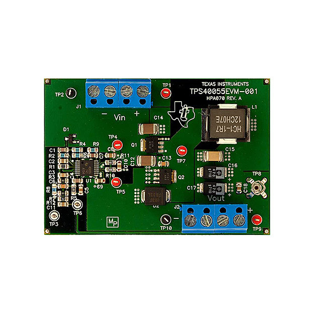
SLUU186 − March 2004 TPS40055-Based Design Converts 12-V Bus to 1.8 V at 15 A (HPA070) Mark Dennis System Power Contents 1 Introduction . . . . . . . . . . . . . . . . . . . . . . . . . . . . . . . . . . . . . . . . . . . . . . . . . . . . . . . . . . . . . . . . . . . . . . . . . 4 2 Features . . . . . . . . . . . . . . . . . . . . . . . . . . . . . . . . . . . . . . . . . . . . . . . . . . . . . . . . . . . . . . . . . . . . . . . . . . . . 4 3 Schematic . . . . . . . . . . . . . . . . . . . . . . . . . . . . . . . . . . . . . . . . . . . . . . . . . . . . . . . . . . . . . . . . . . . . . . . . . . . 5 4 Component Selection . . . . . . . . . . . . . . . . . . . . . . . . . . . . . . . . . . . . . . . . . . . . . . . . . . . . . . . . . . . . . . . 6 5 Test Setup . . . . . . . . . . . . . . . . . . . . . . . . . . . . . . . . . . . . . . . . . . . . . . . . . . . . . . . . . . . . . . . . . . . . . . . . . . 10 6 Test Results and Performance Data . . . . . . . . . . . . . . . . . . . . . . . . . . . . . . . . . . . . . . . . . . . . . . . . . 11 7 EVM Assembly Drawing and PCB Layout . . . . . . . . . . . . . . . . . . . . . . . . . . . . . . . . . . . . . . . . . . . . . 12 8 List of Materials . . . . . . . . . . . . . . . . . . . . . . . . . . . . . . . . . . . . . . . . . . . . . . . . . . . . . . . . . . . . . . . . . . . . 15 9 References . . . . . . . . . . . . . . . . . . . . . . . . . . . . . . . . . . . . . . . . . . . . . . . . . . . . . . . . . . . . . . . . . . . . . . . . . 16 1 Introduction In many modern electronic applications there is a growing demand for circuits to convert a12-V bus to digital voltages as low as, but not limited to 1.8 V. The current requirements can range from below 1 A to over 15 A. For high-efficiency and small circuit size the TPS40055 wide-input synchronous buck controller can be used to provide the necessary control and drive functions to implement these converters. The TPS40055EVM−001 operates at 300 kHz and delivers 1.8 V at 15 A with efficiency over 90% for much of the load range, and a full load efficiency of 88%. The TPS40055 synchronous buck controller offers a variety of user programmable functions such as operating frequency, soft-start time, voltage feed-forward, high-side current limit, and external loop compensation. This controller also provides a regulated 10-V bias voltage which supplies onboard drivers for the N-channel switch and synchronous rectifier MOSFETs, utilizing adaptive gate drive logic to prevent cross conduction of the power MOSFETs.[1] 2 Features The specification of this design is as follows: (cid:1) 92% peak efficiency at 6 A (cid:1) 88% peak efficiency at 15 A (cid:1) 1.8V output at 15 A (cid:1) V range from 10 V to 14 V IN DC DC (cid:1) Small circuit size 1.4” x 2.5” SMT design, components on single side (cid:1) Line/load regulation < 0.5% (cid:1) High-frequency 300-kHz operation (cid:1) Transient deviation 60 mV with 10-A load step 4 TPS40055-Based Design Converts 12-V Bus to 1.8 V at 15 A (HPA070)
SLUU186 − March 2004 3 Schematic + + Figure 1. TPS40055EVM−001 (HPA070) Schematic TPS40055-Based Design Converts 12-V Bus to 1.8 V at 15 A (HPA070) 5
SLUU186 − March 2004 4 Component Selection 4.1 TPS40055 Device Selection The TPS4005x family of parts offers a range of output current configurations including source only (TPS40054), source/sink (TPS40055), or source/sink with V prebias (TPS40057). In this converter the TPS40055 with OUT source/sink capability is selected. This serves to maintain continuous inductor ripple current all the way to zero load to improve the small signal loop response by preventing the inductor current from transitioning to the discontinuous current mode. The TPS4005x family is packaged in TI’s PWP PowerPAD thermally enhanced package which should be soldered to the PCB using standard solder flow techniques. The PowerPAD technology uses a thermally conductive epoxy to attach the integrated circuit die to the leadframe die pad, which is exposed on the bottom of the completed package. The PWP PowerPAD package has a θ = 2°C/W which helps keep the junction JC temperature rise relatively low even with the power dissipation inherent in the onboard MOSFET drivers. This power loss is proportional to switching frequency, drive voltage, and the gate charge needed to enhance the N-channel MOSFETs. Effective heat removal allows the use of ultra-small packaging while maintaining high component reliability. The technical brief, PowerPAD Thermally Enhanced Package[2] contains more information on the PowerPAD package. 4.2 Frequency of Operation The clock oscillator frequency for the TPS40055 is programmed with a single resistor from RT (pin 2) to signal ground. The following equation (1) from the datasheet allows selection of RT in kΩ for a given switching frequency in kHz. R (cid:1) R2 (cid:1) 1 (cid:3)23 (k(cid:1)) (1) T f (cid:2)17.82(cid:2)10(cid:3)6 SW For 300-kHz operation, R2 is selected to be 165 kΩ. For a particular operating frequency, the PWM ramp time must be programmed via the resistor R connected KFF to V . Also, the selection of R programs the V voltage at which the circuit starts operation. This prevents IN KFF IN the circuit from starting at low voltages, which can lead to current flow larger than desired. R is programmed KFF using equation (2). (cid:4) (cid:5) (cid:4) (cid:5) R (cid:1) R6 (cid:1) V (cid:3)3.5 (cid:2) 58.14(cid:2)R (cid:6)1340 (k(cid:1)) (2) KFF IN(min) T Where VIN(min) is the minimum startup input voltage, and RT is in kΩ. Note that internal tolerances have been incorporated into this equation, so the actual VIN(min) of the input voltage should be used. For an oscillator frequency of 300-kHz, the RKFF value of 71.5 kΩ is selected. 6 TPS40055-Based Design Converts 12-V Bus to 1.8 V at 15 A (HPA070)
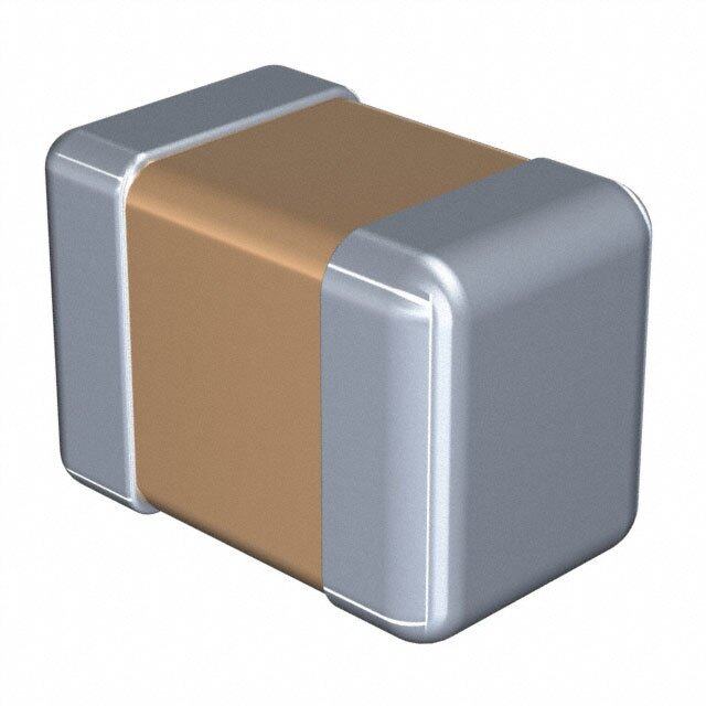
SLUU186 − March 2004 4.3 UVLO Circuitry The user programmable UVLO built into the TPS4005x provides hysteresis for transients shorter than a total count of seven cycles. If the input voltage to the converter can be slowly rising around the minimum V range, IN external hysteresis can be incorporated to prevent multiple on/off cycles during startup or shutdown. These on/off cycles are a result of line impedance external to the EVM causing V to the module to drop when under IN load, which causes the programmable UVLO threshold to be crossed repetitively. In this converter, C1 and D1 are added to form a peak detector from the lower gate drive which is only active when the converter is operating. This provides a bias source to deliver hysteresis current from the peak detector voltage to the lower KFF voltage of 3.5 V, enabling the designer to alter the programmable UVLO shutdown point. The bias is not present during startup, so the circuit starts as expected from the R calculation. KFF In this application, R4 is selected to provide a hysteresis current of 20% I . R4 can be calculated from equation KFF (3). (cid:4) (cid:5) R (cid:2) V (cid:3)3.5 R (cid:1) R4 (cid:1) KFF(cid:4) PD (cid:5) (3) HYS 0.2(cid:2) V (cid:3)3.5 IN(min) where (cid:1) V is the voltage on the peak detector PD (cid:1) VIN(min) is the desired start voltage used in the determination of RKFF In a typical case, V = 8V, and R4 is found to be 247 kΩ, and a standard value of 243kΩ is selected. Testing PD shows the startup voltage to be 9.2 V, and the shutdown voltage to be 8.5 V. 4.4 Inductance Value The output inductor L1 value used in the circuit of Figure 2 was selected from equation (4). V V L (cid:1) OUT (cid:2)1(cid:3) OUT (4) f(cid:2)I V RIPPLE IN(min) in which I is usually chosen to be in the range between 10% and 40% of I . With I = 20% of RIPPLE OUT RIPPLE IOUT(max) there is a ripple current of 3 A, and the inductance value is 1.7 µH. 4.5 Input capacitor selection Bulk input capacitor selection is based on allowable input voltage ripple and required RMS current carrying capability. In typical buck converter applications, the converter is fed from an upstream power converter with its own output capacitance. In this converter, ceramic capacitors capable of meeting circuit requirements are provided onboard. For this power level, input voltage ripple of approximately 250 mV is reasonable, and the minimum capacitance is calculated in (5). C (cid:1) I(cid:2)(cid:2) t (cid:1) I(cid:2)VO (cid:1) 15 A(cid:2)1.8 V (cid:1) 36 (cid:3)F (5) IN (cid:2) V (cid:2) V(cid:2)V (cid:2)f 0.25 V(cid:2)10 V(cid:2)300 kHz IN S Also consider the RMS current rating required for the input capacitors (6). (cid:8) (cid:8) V i (cid:7) I (cid:2)(cid:8)D (cid:1) I (cid:2) OUT (cid:1) 15(cid:2) 1.8 (cid:1) 6.4 A (6) OUT OUT V 10 IN To meet this requirement with the smallest cost and size two 22 µF, 16 V, X5R ceramic capacitors (C12, C14) are installed on the board. In the 1812 case, the parts are able to carry approximately 4 ARMS each. These capacitors function as power bypass components and should be located close to the MOSFET packages to keep the high-frequency current flow in a small, tight loop. TPS40055-Based Design Converts 12-V Bus to 1.8 V at 15 A (HPA070) 7
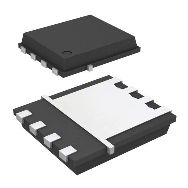
SLUU186 − March 2004 4.6 Output Capacitor Selection Selection of the output capacitor is based on many application variables, including function, cost, size, and availability. The minimum allowable output capacitance is determined by the amount of inductor ripple current and the allowable output ripple, as given in equation (7). I C (cid:1) RIPPLE (cid:1) 3 A (cid:1) 83 (cid:3)F (7) OUT(min) 8(cid:2)f(cid:2)V 8(cid:2)300 kHz(cid:2)15 mV RIPPLE In this design, C is 83 µF with V =15 mV to allow for some margin. However, this only affects the OUT(min) RIPPLE capacitive component of the ripple voltage, and the final value of capacitance is generally influenced by ESR and transient considerations. The voltage component due to the capacitor ESR. V C (cid:9) RIPPLE (cid:1) 15 mA (cid:1) 5 (cid:3)(cid:1) (8) ESR I 3 A RIPPLE An additional consideration in the selection of the output inductor and capacitance value can be derived from examining the transient voltage overshoot which can be initiated with a load step from full load to no load. By equating the inductive energy with the capacitive energy the equation (9) can be derived: (cid:4) (cid:5) (cid:4) (cid:5)2 (cid:4) (cid:5)2 L(cid:2) I (cid:3) I OH OL C (cid:9) L(cid:2)I2 (cid:1) (cid:1) (cid:4) 1.7 (cid:3)H(cid:2)(15 A) (cid:5) (cid:1) 1034 (cid:3)F (9) O V2 (cid:4)V(cid:5)2(cid:3)(cid:4)V(cid:5)2 (1.9 V)2(cid:3)(1.8 V)2 f i where • I = full load current OH • I = no load current OL • Vf = allowed transient voltage rise • V = initial voltage i For compactness while maintaining transient response capability, two 470-µF POSCAP capacitors (C16, C17) are fitted in parallel. The total ESR of these capacitors is approximately 5 mΩ. An additional 47-µF, 6.3-V ceramic capacitor C15 is placed in parallel with the POSCAPs to help suppress high frequency noise generated by the fast current transitions as the current switches between the input and output circuits during each switching cycle. 4.7 MOSFET selection Proper MOSFET selection is essential to optimize circuit efficiency. To operate with high current it is important to choose a package which allows the generated heat to be removed from the package as easily as possible. Various MOSFETs with a package similar to the SO−8 footprint are considered for this application, and devices with reduced junction-case thermal impedance are selected. For the upper switch Q1, a Hitachi HAT2168H MOSFET with low gate charge (typically 27 nC at 10 V) and with an R of 6 mΩ is selected to keep the switching losses to a minimum. The low-side rectifier switch Q2 was DS(on) chosen as a Hitachi HAT2167H, which has slightly more gate charge (43 nC at 10 V) but lower R = 4.2 DS(on) mΩ to minimize conduction losses. A schottky diode, D2, is placed across Q2 in this high current design to carry some of the high circulating current during short circuit conditions. 8 TPS40055-Based Design Converts 12-V Bus to 1.8 V at 15 A (HPA070)
SLUU186 − March 2004 4.8 Short Circuit Protection The TPS40055 implements short circuit protection by comparing the voltage across the topside MOSFET while it is ON to a voltage developed across R due to an internal current source of 10 µA inside pin 16. Both of these LIM voltages are negative with respect to V . From the datasheet equation, R is defined as: IN LIM I (cid:2)R V R (cid:1) R9 (cid:1) OC DS(on)(max) (cid:1) OS (cid:1) ((cid:1)) (10) LIM 1.12(cid:2)I I SINK SINK where • I is the overcurrent set point equal to the DC output current plus one-half the inductor ripple current OC • V is the overcurrent comparator offset, and Isink is the current into ILIM (pin 16). OS Using worst case tolerances the value of R should be maximized to ensure that the converter can deliver full LIM rated current under all conditions. In a worst case condition, R =R9 and LIM R (cid:1) (15 A(cid:6)1.5 A)(cid:2)(7.9 m(cid:1)(cid:2)1.45)(cid:6)(cid:3)30 mV(cid:1) 16.0 k(cid:1) (11) LIM 1.12(cid:2)8.65 (cid:3)A 8.65 (cid:3)A The standard value of 16.2 kΩ was selected. This ensures that we can deliver a minimum of 15 A before current limit is activated. There is also a small capacitor, C7, placed in parallel with R9 to filter the signal. 4.9 Snubber Component Selection Initially, the junction of Q1, Q2, and L1 was ringing at a frequency near 100 MHz with a peak voltage near 30 V. This was due to the extremely fast switching speed of the MOSFETs and the lack of any cross−conduction. C13 was added to shunt the high-frequency ringing to ground and the peak voltage is now below 25 V. 4.10 Compensation Components The TPS40055 uses voltage mode control with feed-forward in conjunction with a high-frequency error amplifier to implement closed loop control. The power circuit L-C double pole corner frequency f occurs at 3.8 kHz, and C the output capacitor ESR zero is located at approximately 38 kHz. The feedback compensation network is implemented to provide two zeroes and three poles. The first pole is placed at the origin to improve DC regulation. The first zero is placed at 2.8 kHz, just below the L-C corner frequency. f (cid:1) 1 (12) Z1 2(cid:4)(cid:2)R5(cid:2)C5 The second zero is selected to be coincident with the L-C corner frequency of 3.8 kHz, f (cid:1) 1 (13) Z2 2(cid:4)(cid:2)(R7(cid:6)R8)(cid:2)C6 The second pole is placed near the ESR zero frequency at 37 kHz. fP1(cid:1) 2(cid:4)(cid:2)R5(cid:2)1(cid:4)C4(cid:2)C5(cid:5) (14) C4(cid:6)C5 and the third pole is placed at 150 kHz, which is one-half the switching frequency. f (cid:1) 1 (15) P2 2(cid:4)(cid:2)R8(cid:2)C6 TPS40055-Based Design Converts 12-V Bus to 1.8 V at 15 A (HPA070) 9
SLUU186 − March 2004 5 Test Setup Figure 2 illustrates the basic test setup needed to evaluate the TPS40055EVM−001. 5.1 DC Input Source The input voltage source should be capable of supplying between 10 V and 14 V and rated for at least 4 DC DC A of current. For best results the input leads should be made with a wire of 18AWG or larger. 5.2 Output Load The output load can be either an electronic load or a resistive load configured to draw between 0 A and 15 A. The output leads should be made with a wire of 16AWG or larger diameter wire. Monitor the output voltage on the PCB by connecting a voltmeter to TP9 and TP10 to prevent voltage drops through PCB traces and the output terminal block which can lead to substantial measurement errors. 5.3 Oscilloscope Probe Test Jacks An oscilloscope probe test jack (TP8) has been included to allow monitoring the ourput voltage ripple. 5.4 Fan There is no cover to prevent the user from probing the internal circuit nodes. There are components that can get hot to the touch (above 60°C) in normal operation. A small fan delivering more than 15 cfm should be used when operating at and near full load. VIN VIN Test Points 10 V to 14 V TP1 = VIN(+) TP2 = VIN(−) − + Fan − + VOUT Test Points TP9 = VOUT(+) TP10 = VOUT(−) VLOAD 1.8 V / 15 A Figure 2. Test Setup 10 TPS40055-Based Design Converts 12-V Bus to 1.8 V at 15 A (HPA070)
SLUU186 − March 2004 6 Test Results / Performance Data 6.1 Efficiency and Power Loss Figure 3 shows the efficiency as the load is varied from 1 A to over 15 A. The typical efficiency remains over 90% as the load ranges from 3 A to 12 A. POWER DISSIPATION EFFICIENCY vs vs LOAD LOAD 94 7 92 6 W 90 n − 5 o % 88 ati y − sip 4 c s n 86 Di Efficie 84 ower 3 P − S 2 82 S DI P 1 80 78 0 0 2 4 6 8 10 12 14 16 0 2 4 6 8 10 12 14 16 IOUT − Output Current − A IOUT − Output Current − A Figure 3 Figure 4 6.2 Closed Loop Performance OVERALL GAIN AND PHASE vs FREQUENCY 50 160 Phase 40 140 30 120 Gain ° 20 100 − B e d s n − 10 80 Pha ai G 0 60 −10 40 −20 20 −30 0 100 1 k 10 k 100 k f − Frequency − kHz Figure 5. TPS40055-Based Design Converts 12-V Bus to 1.8 V at 15 A (HPA070) 11
SLUU186 − March 2004 6.3 Output Ripple and Transient Response Figure 6 shows the typical output voltage ripple with I =15 A to be less than 20 mVpp. OUT The transient response is shown in Figure 7 as the load is stepped from 5 A to 15 A. The voltage deviation is less than 60 mV. OUTPUT VOLTAGE RIPPLE TRANSIENT RESPONSE IOUT = 15 A VOUT = 50 mV/div VRIPPLE (10 mV/div) IOUT 5 A/div t − Time − 1 µs/div t − Time − 200 µs/div Figure 6 Figure 7 7 EVM Assembly Drawing and PCB Layout Figure 8. Top Side Component Assembly 12 TPS40055-Based Design Converts 12-V Bus to 1.8 V at 15 A (HPA070)
SLUU186 − March 2004 Figure 9. Top Side Copper Figure 10. Internal Layer 1 Copper TPS40055-Based Design Converts 12-V Bus to 1.8 V at 15 A (HPA070) 13
SLUU186 − March 2004 Figure 11. Internal Layer 2 Copper Figure 12. Bottom Layer Copper 14 TPS40055-Based Design Converts 12-V Bus to 1.8 V at 15 A (HPA070)
SLUU186 − March 2004 8 List of Materials Table 1 lists the parts values of the evaluation board. These values can be modified to meet the application requirements. Table 1. TPS40055EVM−001 (HPA070) List of Materials REFERENCE QTY DESCRIPTION SIZE MFR PART NUMBER DESIGNATOR C1, C4 2 Capacitor, ceramic, 470 pF, 50 V, X7R, 10% 805 Vishay VJ0805Y471KXAAT C12, C14 2 Capacitor, ceramic, 22 µF, 16 V, X5R, 20% 1812 TDK C4532X5R1C226MT C15 1 Capacitor, ceramic, 47 µF, 6.3 V, X5R, 20% 1812 TDK C4532X5R0J476MT C16, C17(1) 2 Capacitor, POSCAP, 470 µF, 4 V, 10 mΩ, 20% 7343 (D) Sanyo 4TPD470M C2, C8, C10, 5 Capacitor, ceramic, 0.1 µF, 25 V, X7R, 10% 805 Vishay VJ0805Y104KXXAT C11, C18 C3 1 Capacitor, ceramic, 2.2 nF, 50 V, X7R, 10% 805 Vishay VJ0805Y222KXAAT C5 1 Capacitor, ceramic, 5.6 nF, 50 V, X7R, 10% 805 Vishay VJ0805Y562KXAAT C6,C13 2 Capacitor, ceramic, 4.7 nF, 50 V, X7R, 10% 805 Vishay VJ0805Y472KXAAT C7 1 Capacitor, ceramic, 100 pF, 50 V, NPO, 10% 805 Vishay VJ0805A101KXAAT C9 1 Capacitor, ceramic, 1 µF, 16−V, X5R, 10% 805 TDK C2012X5R1C105KT D1 1 Diode, switching, 10 mA, 85 V, 350 mW SOT23 Vishay−Liteon BAS16 D2 1 Diode, schottky, 3 A, 40 V SMC IR 30BQ040 J1, J2 2 Terminal block, 4-pin, 15 A, 5.1 mm 0.80 x 0.35 OST ED2227 L1(1) 1 Inductor, SMT, 1.7−µH, 22.3 A, 1.8 mΩ 0.512 x 0.512 Coiltronics HC1−1R7 Q1(1) 1 MOSFET, N−channel, VDS 30 V, RDS 6 mΩ, ID 30 A LFPAK Hitachi HAT2168H Q2(1) 1 MOSFET, N−channel, VDS 30 V, RDS 4.2 mΩ, ID 40 A LFPAK Hitachi HAT2167H R1 1 Resistor, chip, 1 kΩ, 1/10−W, 1% 805 Std Std R10 1 Resistor, chip, 0 Ω, 1/10−W, 5% 805 Std Std R11 1 Resistor, chip, 0 Ω, 1/10−W, yy% 805 Std Std R12 1 Resistor, chip, 20 Ω, 1/10−W, 5% 805 Std Std R2 1 Resistor, chip, 165 kΩ, 1/10−W, 1% 805 Std Std R3 1 Resistor, chip, 5.49 kΩ, 1/10−W, 1% 805 Std Std R4 1 Resistor, chip, 243 kΩ, 1/10−W, 1% 805 Std Std R5 1 Resistor, chip, 10 kΩ, 1/10−W, 1% 805 Std Std R6 1 Resistor, chip, 71.5 kΩ, 1/10−W, 1% 805 Std Std R7 1 Resistor, chip, 8.66 kΩ, 1/10−W, 1% 805 Std Std R8 1 Resistor, chip, 226 Ω, 1/10−W, 1% 805 Std Std R9 1 Resistor, chip, 16.2 kΩ, 1/10−W, 1% 805 Std Std TP1, TP4, 5 JACK, test point, red Farnell 240−345 TP5, TP7, TP9 TP2, TP3, 4 JACK, test point, black Farnell 240−333 TP6, TP10 131−4244−00 or TP8 1 Adaptor, 3.5 mm probe clip 0.2 Tektronix 131−5031−00 U1 1 Wide input synchronous buck controller PWP16 TI TPS40055PWP −− 1 PCB, 2.85” x 2” x .062 In Std HPA070 TPS40055-Based Design Converts 12-V Bus to 1.8 V at 15 A (HPA070) 15
SLUU186 − March 2004 9 References 1. Data Sheet, TPS40055 Wide-Input Synchronous Buck Controller (SLUS593). 2. Technical Brief, PowerPAD Thermally Enhanced Package (SLMA002). 16 TPS40055-Based Design Converts 12-V Bus to 1.8 V at 15 A (HPA070)
IMPORTANT NOTICE Texas Instruments Incorporated and its subsidiaries (TI) reserve the right to make corrections, modifications, enhancements, improvements, and other changes to its products and services at any time and to discontinue any product or service without notice. Customers should obtain the latest relevant information before placing orders and should verify that such information is current and complete. All products are sold subject to TI’s terms and conditions of sale supplied at the time of order acknowledgment. TI warrants performance of its hardware products to the specifications applicable at the time of sale in accordance with TI’s standard warranty. Testing and other quality control techniques are used to the extent TI deems necessary to support this warranty. Except where mandated by government requirements, testing of all parameters of each product is not necessarily performed. TI assumes no liability for applications assistance or customer product design. Customers are responsible for their products and applications using TI components. To minimize the risks associated with customer products and applications, customers should provide adequate design and operating safeguards. TI does not warrant or represent that any license, either express or implied, is granted under any TI patent right, copyright, mask work right, or other TI intellectual property right relating to any combination, machine, or process in which TI products or services are used. Information published by TI regarding third-party products or services does not constitute a license from TI to use such products or services or a warranty or endorsement thereof. Use of such information may require a license from a third party under the patents or other intellectual property of the third party, or a license from TI under the patents or other intellectual property of TI. Reproduction of information in TI data books or data sheets is permissible only if reproduction is without alteration and is accompanied by all associated warranties, conditions, limitations, and notices. Reproduction of this information with alteration is an unfair and deceptive business practice. TI is not responsible or liable for such altered documentation. Resale of TI products or services with statements different from or beyond the parameters stated by TI for that product or service voids all express and any implied warranties for the associated TI product or service and is an unfair and deceptive business practice. TI is not responsible or liable for any such statements. Following are URLs where you can obtain information on other Texas Instruments products and application solutions: Products Applications Amplifiers amplifier.ti.com Audio www.ti.com/audio Data Converters dataconverter.ti.com Automotive www.ti.com/automotive DSP dsp.ti.com Broadband www.ti.com/broadband Interface interface.ti.com Digital Control www.ti.com/digitalcontrol Logic logic.ti.com Military www.ti.com/military Power Mgmt power.ti.com Optical Networking www.ti.com/opticalnetwork Microcontrollers microcontroller.ti.com Security www.ti.com/security Telephony www.ti.com/telephony Video & Imaging www.ti.com/video Wireless www.ti.com/wireless Mailing Address: Texas Instruments Post Office Box 655303 Dallas, Texas 75265 Copyright 2004, Texas Instruments Incorporated