ICGOO在线商城 > 集成电路(IC) > PMIC - 监控器 > TPS3838L30QDBVRQ1
 Datasheet下载
- 型号: TPS3838L30QDBVRQ1
- 制造商: Texas Instruments
- 库位|库存: xxxx|xxxx
- 要求:
| 数量阶梯 | 香港交货 | 国内含税 |
| +xxxx | $xxxx | ¥xxxx |
查看当月历史价格
查看今年历史价格
TPS3838L30QDBVRQ1产品简介:
ICGOO电子元器件商城为您提供TPS3838L30QDBVRQ1由Texas Instruments设计生产,在icgoo商城现货销售,并且可以通过原厂、代理商等渠道进行代购。 TPS3838L30QDBVRQ1价格参考。Texas InstrumentsTPS3838L30QDBVRQ1封装/规格:PMIC - 监控器, 开路漏极或开路集电极 监控器 1 通道 SOT-23-5。您可以下载TPS3838L30QDBVRQ1参考资料、Datasheet数据手册功能说明书,资料中有TPS3838L30QDBVRQ1 详细功能的应用电路图电压和使用方法及教程。
TPS3838L30QDBVRQ1 是 Texas Instruments(德州仪器)生产的一款电源管理集成电路(PMIC),具体属于监控器类别。它主要用于监测系统中的电源电压,确保系统在电源异常时能够稳定运行或安全关闭。

 应用场景包括:

1. 汽车电子系统:作为汽车电子控制单元(ECU)中的电压监控器,用于监测电池或系统电压,防止因电压过低或过高导致的系统故障。

2. 工业控制系统:在PLC(可编程逻辑控制器)或工业自动化设备中,用于监控供电电压,确保设备在电源异常时及时复位或报警。

3. 通信设备:用于基站、路由器或交换机等通信设备中,监测电源状态,保障设备在复杂环境中的稳定运行。

4. 消费类电子产品:如高端家电、智能仪表等,用于电源监控和系统复位控制。

5. 嵌入式系统和单片机应用:为MCU(微控制器)提供电源监控,确保其在电源不稳定时能正确复位,防止程序跑飞或数据损坏。

该器件具有低功耗、高精度电压检测和可调延迟时间等特点,适用于对电源稳定性要求较高的各种应用场景。
| 参数 | 数值 |
| 产品目录 | 集成电路 (IC) |
| 描述 | IC LP SUPERVISRY CIRCUIT SOT23-5 |
| 产品分类 | |
| 品牌 | Texas Instruments |
| 数据手册 | |
| 产品图片 |
|
| 产品型号 | TPS3838L30QDBVRQ1 |
| rohs | 无铅 / 符合限制有害物质指令(RoHS)规范要求 |
| 产品系列 | - |
| 产品目录页面 | |
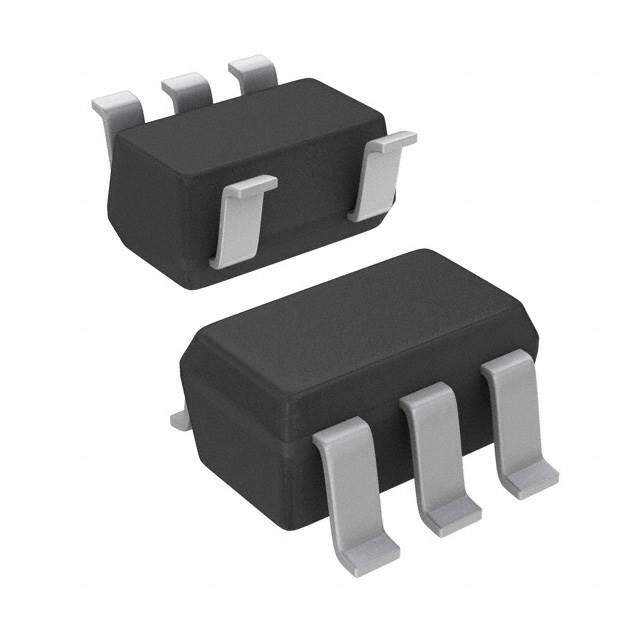
| 供应商器件封装 | SOT-23-5 |
| 其它名称 | 296-15671-6 |
| 包装 | Digi-Reel® |
| 受监控电压数 | 1 |
| 复位 | 低有效 |
| 复位超时 | 最小为 100 ms |
| 安装类型 | 表面贴装 |
| 封装/外壳 | SC-74A,SOT-753 |
| 工作温度 | -40°C ~ 125°C |
| 标准包装 | 1 |
| 电压-阈值 | 2.64V |
| 类型 | 简单复位/加电复位 |
| 输出 | 开路漏极或开路集电极 |


- 商务部:美国ITC正式对集成电路等产品启动337调查
- 曝三星4nm工艺存在良率问题 高通将骁龙8 Gen1或转产台积电
- 太阳诱电将投资9.5亿元在常州建新厂生产MLCC 预计2023年完工
- 英特尔发布欧洲新工厂建设计划 深化IDM 2.0 战略
- 台积电先进制程称霸业界 有大客户加持明年业绩稳了
- 达到5530亿美元!SIA预计今年全球半导体销售额将创下新高
- 英特尔拟将自动驾驶子公司Mobileye上市 估值或超500亿美元
- 三星加码芯片和SET,合并消费电子和移动部门,撤换高东真等 CEO
- 三星电子宣布重大人事变动 还合并消费电子和移动部门
- 海关总署:前11个月进口集成电路产品价值2.52万亿元 增长14.8%


PDF Datasheet 数据手册内容提取
(cid:1) TPS3836E18-Q1 / J25-Q1 / H30-Q1 / L30-Q1 / K33-Q1 TPS3837E18-Q1 / J25-Q1 / L30-Q1 / K33-Q1, TPS3838E18-Q1 / J25-Q1 / L30-Q1 / K33-Q1 NANOPOWER SUPERVISORY CIRCUITS SGLS141A − DECEMBER 2002 − REVISED JANUARY 2007 (cid:1) (cid:1) Qualified for Automotive Applications Applications Include (cid:1) Customer-Specific Configuration Control − Applications Using Automotive Can Be Supported Along With Low-Power DSPs, Microcontrollers, or Major-Change Approval Microprocessors (cid:1) − Battery-Powered Equipment ESD Protection Exceeds 2000 V Per − Intelligent Instruments MIL-STD-883, Method 3015; Exceeds 200 V − Wireless Communication Systems Using Machine Model (C = 200 pF, R = 0) − Automotive Systems (cid:1) Supply Current of 220 nA (Typ) (cid:1) TPS3836, TPS3838 Precision Supply Voltage Supervision DBV PACKAGE Range: 1.8 V, 2.5 V, 3.0 V, 3.3 V (TOP VIEW) (cid:1) Power-On Reset Generator With Selectable Delay Time of 10 ms or 200 ms CT 1 5 VDD (cid:1) Push/Pull RESET Output (TPS3836), GND 2 RESET Output (TPS3837), or Open-Drain RESET Output (TPS3838) MR 3 4 RESET (cid:1) Manual Reset (cid:1) 5-Pin SOT-23 Package TPS3837 (cid:1) Temperature Range: −40°C to 125°C DBV PACKAGE (TOP VIEW) description CT 1 5 VDD The TPS3836, TPS3837, TPS3838 families of GND 2 supervisory circuits provide circuit initialization and timing supervision, primarily for DSP and MR 3 4 RESET processor-based systems. During power on, RESET is asserted when the supply voltage V becomes higher than 1.1 V. Thereafter, the DD supervisory circuit monitors VDD and keeps RESET output active as long as VDD remains below the threshold voltage V . An internal timer delays the return of the output to the inactive state (high) to ensure proper system IT reset. The delay time starts after V has risen above the threshold voltage V . DD IT When CT is connected to GND a fixed delay time of typical 10 ms is asserted. When connected to V the delay DD time is typically 200 ms. When the supply voltage drops below the threshold voltage V , the output becomes active (low) again. IT All the devices of this family have a fixed-sense threshold voltage V set by an internal voltage divider. IT The TPS3836 has an active-low push-pull RESET output. The TPS3837 has active-high push-pull RESET, and TPS3838 integrates an active-low open-drain RESET output. Please be aware that an important notice concerning availability, standard warranty, and use in critical applications of TexasInstruments semiconductor products and disclaimers thereto appears at the end of this data sheet. PRODUCTION DATA information is current as of publication date. Copyright 2007, Texas Instruments Incorporated Products conform to specifications per the terms of Texas Instruments standard warranty. Production processing does not necessarily include testing of all parameters. POST OFFICE BOX 655303 • DALLAS, TEXAS 75265 1
TPS3836E18-Q1 / J25-Q1 / H30-Q1 / L30-Q1 / K33-Q1 (cid:1) TPS3837E18-Q1 / J25-Q1 / L30-Q1 / K33-Q1, TPS3838E18-Q1 / J25-Q1 / L30-Q1 / K33-Q1 NANOPOWER SUPERVISORY CIRCUITS SGLS141A − DECEMBER 2002 − REVISED JANUARY 2007 description (continued) TPS3836K33 MSP430 VDD VCC CT Xin Lithium RESET RST Battery MR Xout Quartz 3.6 V T GND VSS 32 kHz TYPICAL OPERATING CIRCUIT The product spectrum is designed for supply voltages of 1.8 V, 2.5 V, 3 V, and 3.3 V. The circuits are available in a 5-pin SOT-23 package. The TPS3836-Q-Q1, TPS3837-Q-Q1, TPS3838-Q-Q1 families are characterized for operation over a temperature range of −40°C to 125°C. PACKAGE INFORMATION TA DEVICE NAME THRESHOLD VOLTAGE SYMBOL TPS3836E18QDBVRQ1† 1.71 V PDNQ TPS3836J25QDBVRQ1† 2.25 V PDSQ TPS3836H30QDBVRQ1† 2.79 V PHRQ TPS3836L30QDBVRQ1† 2.64 V PCAQ TPS3836K33QDBVRQ1† 2.93 V PDTQ TPS3837E18QDBVRQ1† 1.71 V PDOQ −4400°CC ttoo 112255°CC TPS3837J25QDBVRQ1† 2.25 V PDRQ TPS3837L30QDBVRQ1† 2.64 V PCBQ TPS3837K33QDBVRQ1† 2.93 V PDUQ TPS3838E18QDBVRQ1† 1.71 V PDQQ TPS3838J25QDBVRQ1† 2.25 V PDPQ TPS3838L30QDBVRQ1† 2.64 V PCCQ TPS3838K33QDBVRQ1† 2.93 V PDVQ †DBVR indicates tape and reel of 3000 parts. ORDERING INFORMATION TPS383 6 E 18 Q DBV R Q1 Automotive Designator Reel Package Q-Temperature Designator Nominal Supply Voltage Typical Reset Threshold Voltage Functionality Family 2 POST OFFICE BOX 655303 • DALLAS, TEXAS 75265
(cid:1) TPS3836E18-Q1 / J25-Q1 / H30-Q1 / L30-Q1 / K33-Q1 TPS3837E18-Q1 / J25-Q1 / L30-Q1 / K33-Q1, TPS3838E18-Q1 / J25-Q1 / L30-Q1 / K33-Q1 NANOPOWER SUPERVISORY CIRCUITS SGLS141A − DECEMBER 2002 − REVISED JANUARY 2007 FUNCTION TABLE TPS3836, TPS3837, TPS3838 MR VDD > VIT RESET† RESET‡ L 0 L H L 1 L H H 0 L H H 1 H L †TPS3836 and TPS3838 ‡TPS3837 functional block diagram VDD R3 CT MR R1 C1 Reset Logic Reset (TPS3837-Push-Pull) + and Timer S1 Reset (TPS3836-Push-Pull − TPS3838-Open-Drain) R2 C2 S2 S3 Band-Gap Reference C3 Refresh Timer GND POST OFFICE BOX 655303 • DALLAS, TEXAS 75265 3
TPS3836E18-Q1 / J25-Q1 / H30-Q1 / L30-Q1 / K33-Q1 (cid:1) TPS3837E18-Q1 / J25-Q1 / L30-Q1 / K33-Q1, TPS3838E18-Q1 / J25-Q1 / L30-Q1 / K33-Q1 NANOPOWER SUPERVISORY CIRCUITS SGLS141A − DECEMBER 2002 − REVISED JANUARY 2007 timing diagram A B C D E F G VDD VIT < 1.1 V t MR t RESET t Undefined td td td Undefined Output Output 4 POST OFFICE BOX 655303 • DALLAS, TEXAS 75265
(cid:1) TPS3836E18-Q1 / J25-Q1 / H30-Q1 / L30-Q1 / K33-Q1 TPS3837E18-Q1 / J25-Q1 / L30-Q1 / K33-Q1, TPS3838E18-Q1 / J25-Q1 / L30-Q1 / K33-Q1 NANOPOWER SUPERVISORY CIRCUITS SGLS141A − DECEMBER 2002 − REVISED JANUARY 2007 absolute maximum ratings over operating free-air temperature range (unless otherwise noted)† Supply voltage, V (see Note 1) . . . . . . . . . . . . . . . . . . . . . . . . . . . . . . . . . . . . . . . . . . . . . . . . . . . . . . . . . . . . . . 7 V DD All other pins (see Note 1) . . . . . . . . . . . . . . . . . . . . . . . . . . . . . . . . . . . . . . . . . . . . . . . . . . . . . . . . . . . −0.3 V to 7 V Maximum low output current, I . . . . . . . . . . . . . . . . . . . . . . . . . . . . . . . . . . . . . . . . . . . . . . . . . . . . . . . . . . . . 5 mA OL Maximum high output current, I . . . . . . . . . . . . . . . . . . . . . . . . . . . . . . . . . . . . . . . . . . . . . . . . . . . . . . . . . . −5 mA OH Input clamp current, IIK (VI < 0 or VI > VDD). . . . . . . . . . . . . . . . . . . . . . . . . . . . . . . . . . . . . . . . . . . . . . . . . . ±10 mA Output clamp current, IOK (VO < 0 or VO > VDD) . . . . . . . . . . . . . . . . . . . . . . . . . . . . . . . . . . . . . . . . . . . . . ±10 mA Continuous total power dissipation . . . . . . . . . . . . . . . . . . . . . . . . . . . . . . . . . . . . . . See Dissipation Rating Table Operating free-air temperature range, T . . . . . . . . . . . . . . . . . . . . . . . . . . . . . . . . . . . . . . . . . . . . −40°C to 125°C A Storage temperature range, T . . . . . . . . . . . . . . . . . . . . . . . . . . . . . . . . . . . . . . . . . . . . . . . . . . . . −65°C to 150°C stg Soldering temperature . . . . . . . . . . . . . . . . . . . . . . . . . . . . . . . . . . . . . . . . . . . . . . . . . . . . . . . . . . . . . . . . . . . . 260°C †Stresses beyond those listed under “absolute maximum ratings” may cause permanent damage to the device. These are stress ratings only, and functional operation of the device at these or any other conditions beyond those indicated under “recommended operating conditions” is not implied. Exposure to absolute-maximum-rated conditions for extended periods may affect device reliability. NOTE 1: All voltage values are with respect to GND. For reliable operation, the device must not be operated at 7 V for more than t=1000 h continuously DISSIPATION RATING TABLE PACKAGE TA <25°C DERATING FACTOR TA = 70°C TA = 85°C TA = 125°C POWER RATING ABOVE TA = 25°C POWER RATING POWER RATING POWER RATING DBV 437 mW 3.5 mW/ºC 280 mW 227 mW 87 mW recommended operating conditions at specified temperature range MIN MAX UNIT Supply voltage, VDD 1.6 6 V Input voltage, VI 0 VDD + 0.3 V High-level input voltage, VIH 0.7 × VDD V Low-level input voltage, VIL 0.3 ×VDD V Input transition rise and fall rate at MR, ∆t/∆V 100 ns/V Operating free-air temperature range, TA −40 125 °C POST OFFICE BOX 655303 • DALLAS, TEXAS 75265 5
TPS3836E18-Q1 / J25-Q1 / H30-Q1 / L30-Q1 / K33-Q1 (cid:1) TPS3837E18-Q1 / J25-Q1 / L30-Q1 / K33-Q1, TPS3838E18-Q1 / J25-Q1 / L30-Q1 / K33-Q1 NANOPOWER SUPERVISORY CIRCUITS SGLS141A − DECEMBER 2002 − REVISED JANUARY 2007 electrical characteristics over recommended operating conditions (unless otherwise noted) PARAMETER TEST CONDITION MIN TYP MAX UNIT RREESSEETT VDD = 3.3 V, IOH = −2 mA (TPS3836) VDD = 6 V, IOH = −3 mA 00..88 ×× VVOH HHiigghh-lleevveell oouuttppuutt vvoollttaaggee RREESSEETT VDD = 1.8 V, IOH = −1 mA VDD VV (TPS3837) VDD = 3.3 V, IOL = −2 mA RREESSEETT VDD = 1.8 V, IOL = 1 mA (TPS3836/8) VDD = 3.3 V, IOL = 2 mA VVOL LLooww-lleevveell oouuttppuutt vvoollttaaggee RREESSEETT VDD = 3.3 V, IOL = 2 mA 00.44 VV (TPS3837) VDD = 6 V, IOL = 3 mA TPS3836/8 VDD ≥1.1 V, IOL = 50 µA 0.2 PPoowweerr-uupp rreesseett vvoollttaaggee 0.8 × V (see Note 2) TPS3837 VDD ≥1.1 V, IOH = −50 µA VDD TPS383xE18 1.64 1.71 1.76 TPS383xJ25 2.16 2.25 2.30 NNegattiive-goiing iinputt tthhreshholldd VVIITT vvoollttaaggee ((sseeee NNoottee 33)) TPS383xH30 2.70 2.79 2.85 VV TPS383xL30 2.54 2.64 2.71 TPS383xK33 2.82 2.93 3.10 1.7 V < VIT < 2.5 V 30 VVhhyyss HHyysstteerreessiiss aatt VVDDDD iinnppuutt 2.5 V < VIT < 3.5 V 40 mmVV 3.5 V < VIT < 5 V 50 MR IIIIHH HHiigghh-lleevveell iinnppuutt ccuurrrreenntt (see Note 4) MR = 0.7 × VDD, VDD = 6 V −40 −60 −100 µA CT CT = VDD = 6 V −25 25 nA MR IIIILL LLooww-lleevveell iinnppuutt ccuurrrreenntt (see Note 4) MR = 0 V, VDD = 6 V −130 −200 −340 µA CT CT = 0 V, VDD = 6 V −25 25 nA IOH High-level output current TPS3838 VDD = VIT + 0.2 V, VOH = VDD 25 nA VDD > VIT, VDD < 3 V 220 500 nnAA IIDDDD SSuuppppllyy ccuurrrreenntt VDD > VIT, VDD > 3 V 250 550 VDD < VIT 10 25 µA Internal pullup resistor at MR 30 kΩ CI Input capacitance at MR, CT VI = 0 V to VDD 5 pF NOTES: 2. The lowest voltage at which RESET output becomes active. tr, VDD ≥15 µs/V 3. To ensure best stability of the threshold voltage, a bypass capacitor (ceramic, 0.1 µF) should be placed near the supply terminal. 4. If manual reset is unused, MR should be connected to VDD to minimize current consumption. 6 POST OFFICE BOX 655303 • DALLAS, TEXAS 75265
(cid:1) TPS3836E18-Q1 / J25-Q1 / H30-Q1 / L30-Q1 / K33-Q1 TPS3837E18-Q1 / J25-Q1 / L30-Q1 / K33-Q1, TPS3838E18-Q1 / J25-Q1 / L30-Q1 / K33-Q1 NANOPOWER SUPERVISORY CIRCUITS SGLS141A − DECEMBER 2002 − REVISED JANUARY 2007 timing requirements at RL = 1 MΩ, CL = 50 pF, TA = 25(cid:2)C PARAMETER TEST CONDITIONS MIN TYP MAX UNIT at VDD VIH = VIT + 0.2 V, VIL = VIT − 0.2 V 6 µs tw Pulse width at MR VDD ≥VIT + 0.2 V, VIL = 0.3 × VDD, 1 µs VIH = 0.7 ×VDD switching characteristics at RL = 1 MΩ, CL = 50 pF, TA = 25(cid:2)C PARAMETER TEST CONDITIONS MIN TYP MAX UNIT VDD ≥VIT + 0.2 V, MR = 0.7 × VDD, CT = GND, 5 10 15 See timing diagram ttd DDeellaayy ttiimmee VDD≥ VIT + 0.2 V, mmss MR = 0.7 × VDD, CT = VDD , 100 200 300 See timing diagram ttPPHHLL PPrrooppaaggaattiioonn ((ddeellaayy)) ttiimmee,, hhiigghh-ttoo-llooww-lleevveell oouuttppuutt VDD to RESET delay VVIILH == VVIITT −+ 00..22 VV, 10 µµss ((TTPPSS33883366, TTPPSS33883388)) VIL = 1.6 V 50 ttPPLLHH PPrrooppaaggaattiioonn ((ddeellaayy)) ttiimmee,, llooww-ttoo-hhiigghh-lleevveell oouuttppuutt VDD to RESET delay VVIILH == VVIITT −+ 00..22 VV, 10 µµss ((TTPPSS33883377)) VIL = 1.6 V 50 tPHL Propagation (delay) time, high-to-low-level output M(TRP Sto3 8R3E6S, ETPT Sd3e8la3y8) VVVDIILLD == ≥ 00V..33IT ×× + VV 0DD.DD2 ,,V, 0.1 µs tPLH Propagation (delay) time, low-to-high-level output M(TRP Sto3 8R3E7S)ET delay VIL = 0.7 × VDD 0.1 µs TYPICAL CHARACTERISTICS Table of Graphs FIGURE IDD Supply current vs Supply voltage 1 IMR Manual reset current vs Manual reset voltage 2 VOL Low-level output voltage vs Low-level output current 3 VOH High-level output voltage vs High-level output current 4 Normalized reset threshold voltage vs Free-air temperature 5 Minimum pulse duration at VDD vs VDD Threshold overdrive 6 POST OFFICE BOX 655303 • DALLAS, TEXAS 75265 7
TPS3836E18-Q1 / J25-Q1 / H30-Q1 / L30-Q1 / K33-Q1 (cid:1) TPS3837E18-Q1 / J25-Q1 / L30-Q1 / K33-Q1, TPS3838E18-Q1 / J25-Q1 / L30-Q1 / K33-Q1 NANOPOWER SUPERVISORY CIRCUITS SGLS141A − DECEMBER 2002 − REVISED JANUARY 2007 TYPICAL CHARACTERISTICS SUPPLY CURRENT MANUAL RESET CURRENT vs vs SUPPLY VOLTAGE MANUAL RESET VOLTAGE 10 100 MR = Open VDD = 6 V CT = GND TA = 85°C CT = GND 0 8 A A µ− TA = −40°C µent − 6 TA = 25°C urrent −100 TA = 0°C r C y Cur TA = 0°C eset −200 pl R − SupDD 4 TA = −40°C − Manual −300 TAT A= =8 52°5C°C I 2 R IM −400 0 −500 0 2 4 6 −2 0 2 4 6 VDD − Supply Voltage − V VMR − Manual Reset Voltage − V Figure 1 Figure 2 LOW-LEVEL OUTPUT VOLTAGE HIGH-LEVEL OUTPUT VOLTAGE vs vs LOW-LEVEL OUTPUT CURRENT HIGH-LEVEL OUTPUT CURRENT 2.0 2.0 VDD = 2 V VDD = 2 V MR = OPEN V MR = OPEN V CT = GND − CT = GND − Output Voltage 11..05 TA = 25°C Output Voltage 11..05 TTAA = = 8 255°°CC − Low-Level 0.5 TA = 85°C TA = 0°C − High-Level 0.5 TA = 0°C V OL TA = −40°C V OH TA = −40°C 0.0 0.0 0 1 2 3 4 5 6 7 0 1 2 3 4 5 IOL − Low-Level Output Current − mA IOH − High-Level Output Current − mA Figure 3 Figure 4 8 POST OFFICE BOX 655303 • DALLAS, TEXAS 75265
(cid:1) TPS3836E18-Q1 / J25-Q1 / H30-Q1 / L30-Q1 / K33-Q1 TPS3837E18-Q1 / J25-Q1 / L30-Q1 / K33-Q1, TPS3838E18-Q1 / J25-Q1 / L30-Q1 / K33-Q1 NANOPOWER SUPERVISORY CIRCUITS SGLS141A − DECEMBER 2002 − REVISED JANUARY 2007 TYPICAL CHARACTERISTICS NORMALIZED RESET THRESHOLD VOLTAGE vs FREE-AIR TEMPERATURE 1.001 V e − 1 g a olt V d 0.999 ol h s e r h 0.998 T et s e R ed 0.997 CT = GND, aliz MR = Open m r 0.996 o N 0.995 −40 −15 10 35 60 85 TA − Free-Air Temperature − °C Figure 5 MINIMUM PULSE DURATION AT V DD vs VDD THRESHOLD OVERDRIVE 22 MR = Open 20 CT = GND µs 18 TA = 25°C − DD 16 V at 14 n o ati 12 r u D 10 e s ul 8 P m u 6 m ni 4 Mi 2 0 0 0.2 0.4 0.6 0.8 1 1.2 1.4 1.6 1.8 2 VDD − Threshold Overdrive − V Figure 6 POST OFFICE BOX 655303 • DALLAS, TEXAS 75265 9
PACKAGE OPTION ADDENDUM www.ti.com 22-Dec-2016 PACKAGING INFORMATION Orderable Device Status Package Type Package Pins Package Eco Plan Lead/Ball Finish MSL Peak Temp Op Temp (°C) Device Marking Samples (1) Drawing Qty (2) (6) (3) (4/5) 2U3836E18QDBVRG4Q1 NRND SOT-23 DBV 5 3000 Green (RoHS CU NIPDAU Level-1-260C-UNLIM -40 to 125 PDNQ & no Sb/Br) 2U3836H30QDBVRG4Q1 LIFEBUY SOT-23 DBV 5 3000 Green (RoHS CU NIPDAU Level-1-260C-UNLIM -40 to 125 PHRQ & no Sb/Br) 2U3836J25QDBVRG4Q1 LIFEBUY SOT-23 DBV 5 3000 Green (RoHS CU NIPDAU Level-1-260C-UNLIM -40 to 125 PDSQ & no Sb/Br) 2U3836K33QDBVRG4Q1 LIFEBUY SOT-23 DBV 5 3000 Green (RoHS CU NIPDAU Level-1-260C-UNLIM -40 to 125 PDTQ & no Sb/Br) 2U3836L30QDBVRG4Q1 LIFEBUY SOT-23 DBV 5 3000 Green (RoHS CU NIPDAU Level-1-260C-UNLIM -40 to 125 PCAQ & no Sb/Br) 2U3837L30QDBVRG4Q1 LIFEBUY SOT-23 DBV 5 3000 Green (RoHS CU NIPDAU Level-1-260C-UNLIM -40 to 125 PCBQ & no Sb/Br) 2U3838E18QDBVRG4Q1 LIFEBUY SOT-23 DBV 5 3000 Green (RoHS CU NIPDAU Level-1-260C-UNLIM -40 to 125 PDQQ & no Sb/Br) 2U3838J25QDBVRG4Q1 LIFEBUY SOT-23 DBV 5 3000 Green (RoHS CU NIPDAU Level-1-260C-UNLIM -40 to 125 PDPQ & no Sb/Br) 2U3838K33QDBVRG4Q1 ACTIVE SOT-23 DBV 5 3000 Green (RoHS CU NIPDAU Level-1-260C-UNLIM -40 to 125 PDVQ & no Sb/Br) 2U3838L30QDBVRG4Q1 LIFEBUY SOT-23 DBV 5 3000 Green (RoHS CU NIPDAU Level-1-260C-UNLIM -40 to 125 PCCQ & no Sb/Br) TPS3836E18QDBVRQ1 LIFEBUY SOT-23 DBV 5 3000 Green (RoHS CU NIPDAU Level-1-260C-UNLIM -40 to 125 PDNQ & no Sb/Br) TPS3836H30QDBVRQ1 LIFEBUY SOT-23 DBV 5 3000 Green (RoHS CU NIPDAU Level-1-260C-UNLIM -40 to 125 PHRQ & no Sb/Br) TPS3836J25QDBVRQ1 ACTIVE SOT-23 DBV 5 3000 Green (RoHS CU NIPDAU Level-1-260C-UNLIM -40 to 125 PDSQ & no Sb/Br) TPS3836K33QDBVRQ1 ACTIVE SOT-23 DBV 5 3000 Green (RoHS CU NIPDAU Level-1-260C-UNLIM -40 to 125 PDTQ & no Sb/Br) TPS3836L30QDBVRQ1 LIFEBUY SOT-23 DBV 5 3000 Green (RoHS CU NIPDAU Level-1-260C-UNLIM -40 to 125 PCAQ & no Sb/Br) TPS3837E18QDBVRQ1 OBSOLETE SOT-23 DBV 5 TBD Call TI Call TI -40 to 125 TPS3837J25QDBVRQ1 OBSOLETE SOT-23 DBV 5 TBD Call TI Call TI -40 to 125 TPS3837K33QDBVRQ1 OBSOLETE SOT-23 DBV 5 TBD Call TI Call TI -40 to 125 Addendum-Page 1
PACKAGE OPTION ADDENDUM www.ti.com 22-Dec-2016 Orderable Device Status Package Type Package Pins Package Eco Plan Lead/Ball Finish MSL Peak Temp Op Temp (°C) Device Marking Samples (1) Drawing Qty (2) (6) (3) (4/5) TPS3837L30QDBVRQ1 LIFEBUY SOT-23 DBV 5 3000 Green (RoHS CU NIPDAU Level-1-260C-UNLIM -40 to 125 PCBQ & no Sb/Br) TPS3838E18QDBVRQ1 LIFEBUY SOT-23 DBV 5 3000 Green (RoHS CU NIPDAU Level-1-260C-UNLIM -40 to 125 PDQQ & no Sb/Br) TPS3838J25QDBVRQ1 LIFEBUY SOT-23 DBV 5 3000 Green (RoHS CU NIPDAU Level-1-260C-UNLIM -40 to 125 PDPQ & no Sb/Br) TPS3838K33QDBVRQ1 ACTIVE SOT-23 DBV 5 3000 Green (RoHS CU NIPDAU Level-1-260C-UNLIM -40 to 125 PDVQ & no Sb/Br) TPS3838L30QDBVRQ1 NRND SOT-23 DBV 5 3000 Green (RoHS CU NIPDAU Level-1-260C-UNLIM -40 to 125 PCCQ & no Sb/Br) (1) The marketing status values are defined as follows: ACTIVE: Product device recommended for new designs. LIFEBUY: TI has announced that the device will be discontinued, and a lifetime-buy period is in effect. NRND: Not recommended for new designs. Device is in production to support existing customers, but TI does not recommend using this part in a new design. PREVIEW: Device has been announced but is not in production. Samples may or may not be available. OBSOLETE: TI has discontinued the production of the device. (2) Eco Plan - The planned eco-friendly classification: Pb-Free (RoHS), Pb-Free (RoHS Exempt), or Green (RoHS & no Sb/Br) - please check http://www.ti.com/productcontent for the latest availability information and additional product content details. TBD: The Pb-Free/Green conversion plan has not been defined. Pb-Free (RoHS): TI's terms "Lead-Free" or "Pb-Free" mean semiconductor products that are compatible with the current RoHS requirements for all 6 substances, including the requirement that lead not exceed 0.1% by weight in homogeneous materials. Where designed to be soldered at high temperatures, TI Pb-Free products are suitable for use in specified lead-free processes. Pb-Free (RoHS Exempt): This component has a RoHS exemption for either 1) lead-based flip-chip solder bumps used between the die and package, or 2) lead-based die adhesive used between the die and leadframe. The component is otherwise considered Pb-Free (RoHS compatible) as defined above. Green (RoHS & no Sb/Br): TI defines "Green" to mean Pb-Free (RoHS compatible), and free of Bromine (Br) and Antimony (Sb) based flame retardants (Br or Sb do not exceed 0.1% by weight in homogeneous material) (3) MSL, Peak Temp. - The Moisture Sensitivity Level rating according to the JEDEC industry standard classifications, and peak solder temperature. (4) There may be additional marking, which relates to the logo, the lot trace code information, or the environmental category on the device. (5) Multiple Device Markings will be inside parentheses. Only one Device Marking contained in parentheses and separated by a "~" will appear on a device. If a line is indented then it is a continuation of the previous line and the two combined represent the entire Device Marking for that device. (6) Lead/Ball Finish - Orderable Devices may have multiple material finish options. Finish options are separated by a vertical ruled line. Lead/Ball Finish values may wrap to two lines if the finish value exceeds the maximum column width. Addendum-Page 2
PACKAGE OPTION ADDENDUM www.ti.com 22-Dec-2016 Important Information and Disclaimer:The information provided on this page represents TI's knowledge and belief as of the date that it is provided. TI bases its knowledge and belief on information provided by third parties, and makes no representation or warranty as to the accuracy of such information. Efforts are underway to better integrate information from third parties. TI has taken and continues to take reasonable steps to provide representative and accurate information but may not have conducted destructive testing or chemical analysis on incoming materials and chemicals. TI and TI suppliers consider certain information to be proprietary, and thus CAS numbers and other limited information may not be available for release. In no event shall TI's liability arising out of such information exceed the total purchase price of the TI part(s) at issue in this document sold by TI to Customer on an annual basis. OTHER QUALIFIED VERSIONS OF TPS3836-Q1, TPS3836E18-Q1, TPS3836H30-Q1, TPS3836J25-Q1, TPS3836K33-Q1, TPS3836L30-Q1, TPS3837E18-Q1, TPS3837J25-Q1, TPS3837K33-Q1, TPS3837L30-Q1, TPS3838-Q1, TPS3838E18-Q1, TPS3838J25-Q1, TPS3838K33-Q1, TPS3838L30-Q1 : •Catalog: TPS3836, TPS3836E18, TPS3836H30, TPS3836J25, TPS3836K33, TPS3836L30, TPS3837E18, TPS3837J25, TPS3837K33, TPS3837L30, TPS3838, TPS3838E18, TPS3838J25, TPS3838K33, TPS3838L30 •Enhanced Product: TPS3836-EP, TPS3836J25-EP, TPS3837K33-EP NOTE: Qualified Version Definitions: •Catalog - TI's standard catalog product •Enhanced Product - Supports Defense, Aerospace and Medical Applications Addendum-Page 3
PACKAGE MATERIALS INFORMATION www.ti.com 22-Dec-2016 TAPE AND REEL INFORMATION *Alldimensionsarenominal Device Package Package Pins SPQ Reel Reel A0 B0 K0 P1 W Pin1 Type Drawing Diameter Width (mm) (mm) (mm) (mm) (mm) Quadrant (mm) W1(mm) 2U3836E18QDBVRG4Q1 SOT-23 DBV 5 3000 180.0 9.0 3.15 3.2 1.4 4.0 8.0 Q3 2U3836H30QDBVRG4Q1 SOT-23 DBV 5 3000 180.0 9.0 3.15 3.2 1.4 4.0 8.0 Q3 2U3836J25QDBVRG4Q1 SOT-23 DBV 5 3000 180.0 9.0 3.15 3.2 1.4 4.0 8.0 Q3 2U3836K33QDBVRG4Q1 SOT-23 DBV 5 3000 180.0 9.0 3.15 3.2 1.4 4.0 8.0 Q3 2U3836L30QDBVRG4Q1 SOT-23 DBV 5 3000 180.0 9.0 3.15 3.2 1.4 4.0 8.0 Q3 2U3837L30QDBVRG4Q1 SOT-23 DBV 5 3000 180.0 9.0 3.15 3.2 1.4 4.0 8.0 Q3 2U3838E18QDBVRG4Q1 SOT-23 DBV 5 3000 180.0 9.0 3.15 3.2 1.4 4.0 8.0 Q3 2U3838J25QDBVRG4Q1 SOT-23 DBV 5 3000 180.0 9.0 3.15 3.2 1.4 4.0 8.0 Q3 2U3838K33QDBVRG4Q1 SOT-23 DBV 5 3000 180.0 9.0 3.15 3.2 1.4 4.0 8.0 Q3 2U3838L30QDBVRG4Q1 SOT-23 DBV 5 3000 180.0 9.0 3.15 3.2 1.4 4.0 8.0 Q3 TPS3836E18QDBVRQ1 SOT-23 DBV 5 3000 180.0 9.0 3.15 3.2 1.4 4.0 8.0 Q3 TPS3836H30QDBVRQ1 SOT-23 DBV 5 3000 180.0 9.0 3.15 3.2 1.4 4.0 8.0 Q3 TPS3836J25QDBVRQ1 SOT-23 DBV 5 3000 180.0 9.0 3.15 3.2 1.4 4.0 8.0 Q3 TPS3836K33QDBVRQ1 SOT-23 DBV 5 3000 180.0 9.0 3.15 3.2 1.4 4.0 8.0 Q3 TPS3836L30QDBVRQ1 SOT-23 DBV 5 3000 180.0 9.0 3.15 3.2 1.4 4.0 8.0 Q3 TPS3837L30QDBVRQ1 SOT-23 DBV 5 3000 180.0 9.0 3.15 3.2 1.4 4.0 8.0 Q3 TPS3838E18QDBVRQ1 SOT-23 DBV 5 3000 180.0 9.0 3.15 3.2 1.4 4.0 8.0 Q3 TPS3838J25QDBVRQ1 SOT-23 DBV 5 3000 180.0 9.0 3.15 3.2 1.4 4.0 8.0 Q3 PackMaterials-Page1
PACKAGE MATERIALS INFORMATION www.ti.com 22-Dec-2016 Device Package Package Pins SPQ Reel Reel A0 B0 K0 P1 W Pin1 Type Drawing Diameter Width (mm) (mm) (mm) (mm) (mm) Quadrant (mm) W1(mm) TPS3838K33QDBVRQ1 SOT-23 DBV 5 3000 180.0 9.0 3.15 3.2 1.4 4.0 8.0 Q3 TPS3838L30QDBVRQ1 SOT-23 DBV 5 3000 180.0 9.0 3.15 3.2 1.4 4.0 8.0 Q3 *Alldimensionsarenominal Device PackageType PackageDrawing Pins SPQ Length(mm) Width(mm) Height(mm) 2U3836E18QDBVRG4Q1 SOT-23 DBV 5 3000 182.0 182.0 20.0 2U3836H30QDBVRG4Q1 SOT-23 DBV 5 3000 182.0 182.0 20.0 2U3836J25QDBVRG4Q1 SOT-23 DBV 5 3000 182.0 182.0 20.0 2U3836K33QDBVRG4Q1 SOT-23 DBV 5 3000 182.0 182.0 20.0 2U3836L30QDBVRG4Q1 SOT-23 DBV 5 3000 182.0 182.0 20.0 2U3837L30QDBVRG4Q1 SOT-23 DBV 5 3000 182.0 182.0 20.0 2U3838E18QDBVRG4Q1 SOT-23 DBV 5 3000 182.0 182.0 20.0 2U3838J25QDBVRG4Q1 SOT-23 DBV 5 3000 182.0 182.0 20.0 2U3838K33QDBVRG4Q1 SOT-23 DBV 5 3000 182.0 182.0 20.0 2U3838L30QDBVRG4Q1 SOT-23 DBV 5 3000 182.0 182.0 20.0 TPS3836E18QDBVRQ1 SOT-23 DBV 5 3000 182.0 182.0 20.0 TPS3836H30QDBVRQ1 SOT-23 DBV 5 3000 182.0 182.0 20.0 TPS3836J25QDBVRQ1 SOT-23 DBV 5 3000 182.0 182.0 20.0 TPS3836K33QDBVRQ1 SOT-23 DBV 5 3000 182.0 182.0 20.0 TPS3836L30QDBVRQ1 SOT-23 DBV 5 3000 182.0 182.0 20.0 PackMaterials-Page2
PACKAGE MATERIALS INFORMATION www.ti.com 22-Dec-2016 Device PackageType PackageDrawing Pins SPQ Length(mm) Width(mm) Height(mm) TPS3837L30QDBVRQ1 SOT-23 DBV 5 3000 182.0 182.0 20.0 TPS3838E18QDBVRQ1 SOT-23 DBV 5 3000 182.0 182.0 20.0 TPS3838J25QDBVRQ1 SOT-23 DBV 5 3000 182.0 182.0 20.0 TPS3838K33QDBVRQ1 SOT-23 DBV 5 3000 182.0 182.0 20.0 TPS3838L30QDBVRQ1 SOT-23 DBV 5 3000 182.0 182.0 20.0 PackMaterials-Page3
None
None
IMPORTANTNOTICE TexasInstrumentsIncorporatedanditssubsidiaries(TI)reservetherighttomakecorrections,enhancements,improvementsandother changestoitssemiconductorproductsandservicesperJESD46,latestissue,andtodiscontinueanyproductorserviceperJESD48,latest issue.Buyersshouldobtainthelatestrelevantinformationbeforeplacingordersandshouldverifythatsuchinformationiscurrentand complete.Allsemiconductorproducts(alsoreferredtohereinas“components”)aresoldsubjecttoTI’stermsandconditionsofsale suppliedatthetimeoforderacknowledgment. TIwarrantsperformanceofitscomponentstothespecificationsapplicableatthetimeofsale,inaccordancewiththewarrantyinTI’sterms andconditionsofsaleofsemiconductorproducts.TestingandotherqualitycontroltechniquesareusedtotheextentTIdeemsnecessary tosupportthiswarranty.Exceptwheremandatedbyapplicablelaw,testingofallparametersofeachcomponentisnotnecessarily performed. TIassumesnoliabilityforapplicationsassistanceorthedesignofBuyers’products.Buyersareresponsiblefortheirproductsand applicationsusingTIcomponents.TominimizetherisksassociatedwithBuyers’productsandapplications,Buyersshouldprovide adequatedesignandoperatingsafeguards. TIdoesnotwarrantorrepresentthatanylicense,eitherexpressorimplied,isgrantedunderanypatentright,copyright,maskworkright,or otherintellectualpropertyrightrelatingtoanycombination,machine,orprocessinwhichTIcomponentsorservicesareused.Information publishedbyTIregardingthird-partyproductsorservicesdoesnotconstitutealicensetousesuchproductsorservicesorawarrantyor endorsementthereof.Useofsuchinformationmayrequirealicensefromathirdpartyunderthepatentsorotherintellectualpropertyofthe thirdparty,oralicensefromTIunderthepatentsorotherintellectualpropertyofTI. ReproductionofsignificantportionsofTIinformationinTIdatabooksordatasheetsispermissibleonlyifreproductioniswithoutalteration andisaccompaniedbyallassociatedwarranties,conditions,limitations,andnotices.TIisnotresponsibleorliableforsuchaltered documentation.Informationofthirdpartiesmaybesubjecttoadditionalrestrictions. ResaleofTIcomponentsorserviceswithstatementsdifferentfromorbeyondtheparametersstatedbyTIforthatcomponentorservice voidsallexpressandanyimpliedwarrantiesfortheassociatedTIcomponentorserviceandisanunfairanddeceptivebusinesspractice. TIisnotresponsibleorliableforanysuchstatements. Buyeracknowledgesandagreesthatitissolelyresponsibleforcompliancewithalllegal,regulatoryandsafety-relatedrequirements concerningitsproducts,andanyuseofTIcomponentsinitsapplications,notwithstandinganyapplications-relatedinformationorsupport thatmaybeprovidedbyTI.Buyerrepresentsandagreesthatithasallthenecessaryexpertisetocreateandimplementsafeguardswhich anticipatedangerousconsequencesoffailures,monitorfailuresandtheirconsequences,lessenthelikelihoodoffailuresthatmightcause harmandtakeappropriateremedialactions.BuyerwillfullyindemnifyTIanditsrepresentativesagainstanydamagesarisingoutoftheuse ofanyTIcomponentsinsafety-criticalapplications. Insomecases,TIcomponentsmaybepromotedspecificallytofacilitatesafety-relatedapplications.Withsuchcomponents,TI’sgoalisto helpenablecustomerstodesignandcreatetheirownend-productsolutionsthatmeetapplicablefunctionalsafetystandardsand requirements.Nonetheless,suchcomponentsaresubjecttotheseterms. NoTIcomponentsareauthorizedforuseinFDAClassIII(orsimilarlife-criticalmedicalequipment)unlessauthorizedofficersoftheparties haveexecutedaspecialagreementspecificallygoverningsuchuse. OnlythoseTIcomponentswhichTIhasspecificallydesignatedasmilitarygradeor“enhancedplastic”aredesignedandintendedforusein military/aerospaceapplicationsorenvironments.BuyeracknowledgesandagreesthatanymilitaryoraerospaceuseofTIcomponents whichhavenotbeensodesignatedissolelyattheBuyer'srisk,andthatBuyerissolelyresponsibleforcompliancewithalllegaland regulatoryrequirementsinconnectionwithsuchuse. TIhasspecificallydesignatedcertaincomponentsasmeetingISO/TS16949requirements,mainlyforautomotiveuse.Inanycaseofuseof non-designatedproducts,TIwillnotberesponsibleforanyfailuretomeetISO/TS16949. Products Applications Audio www.ti.com/audio AutomotiveandTransportation www.ti.com/automotive Amplifiers amplifier.ti.com CommunicationsandTelecom www.ti.com/communications DataConverters dataconverter.ti.com ComputersandPeripherals www.ti.com/computers DLP®Products www.dlp.com ConsumerElectronics www.ti.com/consumer-apps DSP dsp.ti.com EnergyandLighting www.ti.com/energy ClocksandTimers www.ti.com/clocks Industrial www.ti.com/industrial Interface interface.ti.com Medical www.ti.com/medical Logic logic.ti.com Security www.ti.com/security PowerMgmt power.ti.com Space,AvionicsandDefense www.ti.com/space-avionics-defense Microcontrollers microcontroller.ti.com VideoandImaging www.ti.com/video RFID www.ti-rfid.com OMAPApplicationsProcessors www.ti.com/omap TIE2ECommunity e2e.ti.com WirelessConnectivity www.ti.com/wirelessconnectivity MailingAddress:TexasInstruments,PostOfficeBox655303,Dallas,Texas75265 Copyright©2016,TexasInstrumentsIncorporated