ICGOO在线商城 > 集成电路(IC) > PMIC - 监控器 > TPS3825-33QDBVRQ1
 Datasheet下载
- 型号: TPS3825-33QDBVRQ1
- 制造商: Texas Instruments
- 库位|库存: xxxx|xxxx
- 要求:
| 数量阶梯 | 香港交货 | 国内含税 |
| +xxxx | $xxxx | ¥xxxx |
查看当月历史价格
查看今年历史价格
TPS3825-33QDBVRQ1产品简介:
ICGOO电子元器件商城为您提供TPS3825-33QDBVRQ1由Texas Instruments设计生产,在icgoo商城现货销售,并且可以通过原厂、代理商等渠道进行代购。 TPS3825-33QDBVRQ1价格参考¥6.45-¥11.49。Texas InstrumentsTPS3825-33QDBVRQ1封装/规格:PMIC - 监控器, 推挽式,图腾柱 监控器 1 通道 SOT-23-5。您可以下载TPS3825-33QDBVRQ1参考资料、Datasheet数据手册功能说明书,资料中有TPS3825-33QDBVRQ1 详细功能的应用电路图电压和使用方法及教程。
| 参数 | 数值 |
| 产品目录 | 集成电路 (IC)半导体 |
| 描述 | IC 2.93V SUPPLY MONITOR SOT23-5监控电路 Processor Sup Circuits |
| 产品分类 | |
| 品牌 | Texas Instruments |
| 产品手册 | |
| 产品图片 |
|
| rohs | 符合RoHS无铅 / 符合限制有害物质指令(RoHS)规范要求 |
| 产品系列 | 电源管理 IC,监控电路,Texas Instruments TPS3825-33QDBVRQ1- |
| NumberofInputsMonitored | 1 Input |
| 数据手册 | |
| 产品型号 | TPS3825-33QDBVRQ1 |
| 产品种类 | 监控电路 |
| 人工复位 | Manual Reset |
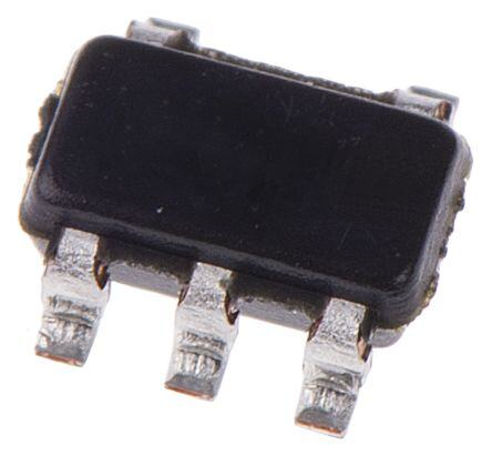
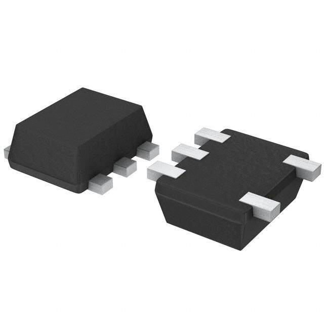
| 供应商器件封装 | SOT-23-5 |
| 其它名称 | 296-15656-1 |
| 功率失效检测 | No |
| 包装 | 剪切带 (CT) |
| 受监控电压数 | 1 |
| 商标 | Texas Instruments |
| 复位 | 低有效 |
| 复位超时 | 最小为 120 ms |
| 安装类型 | 表面贴装 |
| 安装风格 | SMD/SMT |
| 封装 | Reel |
| 封装/外壳 | SC-74A,SOT-753 |
| 封装/箱体 | SOT-23-5 |
| 工作温度 | -40°C ~ 125°C |
| 工作电源电流 | 15 uA |
| 工厂包装数量 | 3000 |
| 最大功率耗散 | 437 mW |
| 最大工作温度 | + 125 C |
| 最小工作温度 | - 40 C |
| 标准包装 | 1 |
| 欠电压阈值 | 2.93 V |
| 电压-阈值 | 2.93V |
| 电池备用开关 | No Backup |
| 电源电压-最大 | 5.5 V |
| 电源电压-最小 | 1.1 V |
| 监视器 | No Watchdog |
| 类型 | 简单复位/加电复位 |
| 系列 | TPS3825-33-Q1 |
| 芯片启用信号 | No Chip Enable |
| 被监测输入数 | 1 Input |
| 输出 | 推挽式,图腾柱 |
| 输出类型 | Push-Pull |
| 过电压阈值 | 3 V |
| 重置延迟时间 | 200 ms |
| 阈值电压 | 2.93 V |


- 商务部:美国ITC正式对集成电路等产品启动337调查
- 曝三星4nm工艺存在良率问题 高通将骁龙8 Gen1或转产台积电
- 太阳诱电将投资9.5亿元在常州建新厂生产MLCC 预计2023年完工
- 英特尔发布欧洲新工厂建设计划 深化IDM 2.0 战略
- 台积电先进制程称霸业界 有大客户加持明年业绩稳了
- 达到5530亿美元!SIA预计今年全球半导体销售额将创下新高
- 英特尔拟将自动驾驶子公司Mobileye上市 估值或超500亿美元
- 三星加码芯片和SET,合并消费电子和移动部门,撤换高东真等 CEO
- 三星电子宣布重大人事变动 还合并消费电子和移动部门
- 海关总署:前11个月进口集成电路产品价值2.52万亿元 增长14.8%


PDF Datasheet 数据手册内容提取
Product Order Technical Tools & Support & Folder Now Documents Software Community TPS3820-Q1,TPS3823-Q1,TPS3824-Q1,TPS3825-Q1,TPS3828-Q1 SGLS143D–DECEMBER2002–REVISEDJULY2019 TPS382x-xx-Q1 Voltage Monitor With Watchdog Timer 1 Features 3 Description • Qualifiedforautomotiveapplications For all new designs with TPS3820-xx-Q1, use the 1 TPS3820-xxQPDBVRQ1 part number. The TPS3820- • AEC-Q100QualifiedWiththeFollowingResults: xxQP is functionally equivalent and a replacement to – Devicetemperaturegrade1: –40°Cto125°C the TPS3820xxQ. The TPS3820-xxQDBVRQ1 is not – DeviceHBMESDclassificationlevel2 recommendedfornewdesigns(NRND). – DeviceCDMESDclassificationlevelC4B The TPS382x-xx-Q1 family of supervisors provide • ESDprotectionexceeds2000VPerMIL-STD- circuit initialization and timing supervision, primarily for DSP and processor-based systems. During power 883,Method3015;usinghumanbodymodel(C= on, RESET asserts when the supply voltage V 100pF,R=1500Ω) DD becomes greater than 1.1 V. Thereafter, the supply • Power-onresetgeneratorwithfixeddelaytimeof voltage supervisor monitors V and keeps RESET DD 200ms(TPS3823/4/5/8-xx-Q1)or25ms active low as long as V remains below the DD (TPS3820-xx-Q1) threshold voltage, V . An internal timer delays the IT− • Manualresetinput(TPS3820/3/5/8-xx-Q1) return of the output to the inactive state (high) to ensure proper system reset. The delay time, t , starts • Resetoutputavailableinactive-low d after V has risen above the threshold voltage V . (TPS3820/3/4/5-xx-Q1),Active-High(TPS3824/5- DD IT− When the supply voltage drops below the threshold xx-Q1),andopendrain(TPS3828-xx-Q1) voltage V , the output becomes active (low) again. IT− • Supplyvoltagesupervisionrange: No external components are required. All the devices 2.5V,3V,3.3V,5V of this family have a fixed-sense threshold voltage, V , set by an internal voltage divider. The TPS382x- • Watchdogtimer(TPS3820/3/4/8-xx-Q1) IT– xx-Q1 family also offers watchdog time out options of • Supplycurrentof15μA(Typical) 200 ms (TPS3820-xx-Q1) and 1.6 s (TPS3823/4/8- • 5-PinSOT-23package xx-Q1). • Temperaturerange:−40°Cto125°C DeviceInformation(1) 2 Applications PARTNUMBER PACKAGE BODYSIZE(NOM) TPS382x-xx-Q1 SOT-23(5) 2.90mm×1.60mm • AutomotiveDSPs,microcontrollers,or microprocessors (1) For all available packages, see the orderable addendum at theendofthedatasheet. • Industrialequipment • Programmablecontrols • Automotivesystems • Portableandbattery-poweredequipment • Intelligentinstruments • Wirelesscommunicationssystems TypicalApplicationSchematic NormalizedInputThresholdVoltagevs Free-AirTemperature 3.3 V °(25C)T 1.001 VDD 100 nF VDD T), VAI 1 (T I RESET RESET −V 0.999 ge TPS3823-33-Q1 MSP430C325 Volta 0.998 d ol MR WDI I/O hresh 0.997 T ut p GND GND d In 0.996 Normalize 0.995−40 −15 10 35 60 85 TA−Free-AirTemperature−°C 1 An IMPORTANT NOTICE at the end of this data sheet addresses availability, warranty, changes, use in safety-critical applications, intellectualpropertymattersandotherimportantdisclaimers.PRODUCTIONDATA.
TPS3820-Q1,TPS3823-Q1,TPS3824-Q1,TPS3825-Q1,TPS3828-Q1 SGLS143D–DECEMBER2002–REVISEDJULY2019 www.ti.com Table of Contents 1 Features.................................................................. 1 8.3 FeatureDescription...................................................9 2 Applications........................................................... 1 8.4 DeviceFunctionalModes........................................10 3 Description............................................................. 1 9 ApplicationandImplementation........................ 11 4 RevisionHistory..................................................... 2 9.1 ApplicationInformation............................................11 9.2 TypicalApplications................................................11 5 DeviceComparisonTable..................................... 3 10 PowerSupplyRecommendations..................... 12 6 PinConfigurationandFunctions......................... 3 11 Layout................................................................... 13 7 Specifications......................................................... 4 11.1 LayoutGuidelines.................................................13 7.1 AbsoluteMaximumRatings......................................4 11.2 LayoutExample....................................................13 7.2 ESDRatings..............................................................4 12 DeviceandDocumentationSupport................. 14 7.3 RecommendedOperatingConditions.......................4 7.4 ThermalInformation..................................................4 12.1 DocumentationSupport........................................14 7.5 ElectricalCharacteristics...........................................5 12.2 ReceivingNotificationofDocumentationUpdates14 7.6 TimingRequirements................................................6 12.3 CommunityResources..........................................14 7.7 SwitchingCharacteristics..........................................6 12.4 Trademarks...........................................................14 7.8 TypicalCharacteristics..............................................7 12.5 ElectrostaticDischargeCaution............................14 12.6 Glossary................................................................14 8 DetailedDescription.............................................. 9 13 Mechanical,Packaging,andOrderable 8.1 Overview...................................................................9 Information........................................................... 15 8.2 FunctionalBlockDiagram.........................................9 4 Revision History NOTE:Pagenumbersforpreviousrevisionsmaydifferfrompagenumbersinthecurrentversion. ChangesfromRevisionC(December2015)toRevisionD Page • Forallnewdesigns,usetheTPS3820-33QPDBVRQ1andTPS3820-50QPDBVRQ1.TPS3820-xxQPisfunctionally equivalentandareplacementtotheTPS3820xxQ................................................................................................................ 1 ChangesfromRevisionB(June2008)toRevisionC Page • AddedESDRatingstable,FeatureDescriptionsection,DeviceFunctionalModes,ApplicationandImplementation section,PowerSupplyRecommendationssection,Layoutsection,DeviceandDocumentationSupportsection,and Mechanical,Packaging,andOrderableInformationsection ................................................................................................. 1 • AddedAEC-Q100QualifiedinformationandTemperatureRangetoFeatures .................................................................... 1 • Added-Q1toallapplicablepartnumbers ............................................................................................................................. 1 • AddedFIXEDDELAYTIMEcolumntotable ........................................................................................................................ 3 2 SubmitDocumentationFeedback Copyright©2002–2019,TexasInstrumentsIncorporated ProductFolderLinks:TPS3820-Q1 TPS3823-Q1 TPS3824-Q1 TPS3825-Q1 TPS3828-Q1
TPS3820-Q1,TPS3823-Q1,TPS3824-Q1,TPS3825-Q1,TPS3828-Q1 www.ti.com SGLS143D–DECEMBER2002–REVISEDJULY2019 5 Device Comparison Table FIXEDDELAY DEVICE RESET RESET WDI MR TIME TPS3820-xx-Q1 Push-pull X X 25ms TPS3823-xx-Q1 Push-pull X X 200ms TPS3824-xx-Q1 Push-pull X 200ms TPS3825-xx-Q1 Push-pull Push-pull X 200ms TPS3828-xx-Q1 Open-drain X X 200ms 6 Pin Configuration and Functions TPS3820-xx-Q1,TPS3823-xx-Q1,TPS3828-xx-Q1:DBV PACKAGE TPS3824-xx-Q1:DBVPACKAGE 5-PinSOT-23 5-PinSOT-23 TopView TopView RESET 1 5 VDD RESET 1 5 VDD GND 2 GND 2 MR 3 4 WDI RESET 3 4 WDI TPS3825-xx-Q1:DBVPACKAGE 5-PinSOT-23 TopView RESET 1 5 VDD GND 2 RESET 3 4 MR PinFunctions PIN TPS3820‑‑xx‑‑Q1, I/O DESCRIPTION NAME TPS3823‑‑xx‑‑Q1, TPS3824‑‑xx‑‑Q1 TPS3825‑‑xx‑‑Q1 TPS3828‑‑xx‑‑Q1 GND 2 2 2 — Groundconnection Manual-resetinput.Pulllowtoforceareset.RESET remainslowaslongasMRislowandforthetime-out MR 3 — 4 I periodafterMRgoeshigh.Leaveunconnectedor connecttoV whenunused. DD Active-highresetoutput.Eitherpush-pulloropen-drain RESET — 3 3 O outputstage. Active-lowresetoutput.Eitherpush-pulloropen-drain RESET 1 1 1 O outputstage. Supplyvoltage.Powersthedeviceandmonitorsitsown V 5 5 5 I DD voltage. Watchdogtimerinput.IfWDIremainshighorlowlonger thanthetime-outperiod,thenresetistriggered.The timerclearswhenresetisassertedorwhenWDIseesa WDI 4 4 — I risingedgeorafallingedge.Ifunused,theWDI connectionmustbehighimpedancetopreventitfrom causingaresetevent. Copyright©2002–2019,TexasInstrumentsIncorporated SubmitDocumentationFeedback 3 ProductFolderLinks:TPS3820-Q1 TPS3823-Q1 TPS3824-Q1 TPS3825-Q1 TPS3828-Q1
TPS3820-Q1,TPS3823-Q1,TPS3824-Q1,TPS3825-Q1,TPS3828-Q1 SGLS143D–DECEMBER2002–REVISEDJULY2019 www.ti.com 7 Specifications 7.1 Absolute Maximum Ratings overoperatingfree-airtemperaturerange(unlessotherwisenoted)(1)(2) MIN MAX UNIT V –0.3 6 DD Voltage V RESET,RESET,MR,WDI –0.3 (V +0.3) DD Maximumlowoutput,I –5 5 OL Current Maximumhighoutput,I –5 5 mA OH Outputrange(V <0orV >V ),I –10 10 O O DD OK Continuoustotalpowerdissipation SeeThermalInformation Operatingfree-air,T –40 125 A Temperature °C Storage,T –65 150 stg (1) StressesbeyondthoselistedunderAbsoluteMaximumRatingsmaycausepermanentdamagetothedevice.Thesearestressratings only,whichdonotimplyfunctionaloperationofthedeviceattheseoranyotherconditionsbeyondthoseindicatedunderRecommended OperatingConditions.Exposuretoabsolute-maximum-ratedconditionsforextendedperiodsmayaffectdevicereliability. (2) AllvoltagevaluesarewithrespecttoGND. 7.2 ESD Ratings VALUE UNIT Human-bodymodel(HBM),perAECQ100-002(1) ±2000 V Electrostaticdischarge V (ESD) Charged-devicemodel(CDM),perAECQ100-011 ±750 (1) AECQ100-002indicatesthatHBMstressingshallbeinaccordancewiththeANSI/ESDA/JEDECJS-001specification. 7.3 Recommended Operating Conditions overoperatingjunctiontemperaturerange(unlessotherwisenoted). MIN NOM MAX UNIT V Supplyvoltage 1.1 5.5 V DD VI Inputvoltage 0 V +0.3 V DD V High-levelinputvoltageatMRandWDI 0.7×V V IH DD V Low-levelinputvoltage 0.3×V V IL DD Δt/ΔV InputtransitionriseandfallrateatMRorWDI 100 ns/V T Operatingfree-airtemperaturerange –40 125 °C A 7.4 Thermal Information TPS382x-xx-Q1 THERMALMETRIC(1) DBV(SOT-23) UNIT 5PINS R Junction-to-ambientthermalresistance 209.1 °C/W θJA R Junction-to-case(top)thermalresistance 72.8 °C/W θJC(top) R Junction-to-boardthermalresistance 36.7 °C/W θJB ψ Junction-to-topcharacterizationparameter 2.1 °C/W JT ψ Junction-to-boardcharacterizationparameter 35.8 °C/W JB (1) Formoreinformationabouttraditionalandnewthermalmetrics,seetheSemiconductorandICPackageThermalMetricsapplication report,SPRA953. 4 SubmitDocumentationFeedback Copyright©2002–2019,TexasInstrumentsIncorporated ProductFolderLinks:TPS3820-Q1 TPS3823-Q1 TPS3824-Q1 TPS3825-Q1 TPS3828-Q1
TPS3820-Q1,TPS3823-Q1,TPS3824-Q1,TPS3825-Q1,TPS3828-Q1 www.ti.com SGLS143D–DECEMBER2002–REVISEDJULY2019 7.5 Electrical Characteristics overoperatingjunctiontemperaturerange(unlessotherwisenoted) PARAMETER TESTCONDITIONS MIN TYP MAX UNIT TPS382x-25-Q1 VDD=VIT−+0.2V,IOH=–20μA TPS382x-30-Q1 0.8×VDD RESET TPS382x-33-Q1 VDD=VIT−+0.2V,IOH=–30μA TPS382x-50-Q1 VDD=VIT−+0.2VIOH=–120μA VDD−1.5V TPS3824-25-Q1 High-leveloutput TPS3825-25-Q1 VDD≥1.8V,IOH=–100μA VOH voltage V TPS3824-30-Q1 TPS3825-30-Q1 RESET 0.8×VDD TPS3824-33-Q1 TPS3825-33-Q1 VDD≥1.8V,IOH=–150μA TPS3824-50-Q1 TPS3825-50-Q1 TPS3824-25-Q1 TPS3825-25-Q1 VDD=VIT−+0.2V,IOL=1mA TPS3824-30-Q1 TPS3825-30-Q1 RESET VDD=VIT−+0.2V,IOL=1.2mA 0.4 TPS3824-33-Q1 TPS3825-33-Q1 Low-leveloutput VOL voltage TPS3824-50-Q1 V TPS3825-50-Q1 VDD=VIT−+0.2V,IOL=3mA TPS382x-25-Q1 VDD=VIT−–0.2V,IOL=1mA TPS382x-30-Q1 RESET VDD=VIT−–0.2V,IOL=1.2mA 0.45 TPS382x-33-Q1 TPS382x-50-Q1 VDD=VIT−–0.2V,IOL=3mA Power-upresetvoltage(1) VDD≥1.1V,IOL=20μA 0.4 V TPS382x-25-Q1 2.21 2.25 2.3 TPS382x-30-Q1 2.59 2.63 2.69 TA=0°Cto85°C TPS382x-33-Q1 2.88 2.93 3 Negative-goinginput TPS382x-50-Q1 4.49 4.55 4.64 VIT− thresholdvoltage(2) TPS382x-25-Q1 2.19 2.25 2.3 V TPS382x-30-Q1 2.55 2.63 2.69 TA=–40°Cto125°C TPS382x-33-Q1 2.84 2.93 3 TPS382x-50-Q1 4.44 4.55 4.64 TPS382x-25-Q1 TPS382x-30-Q1 30 Vhys HysteresisatVDDinput mV TPS382x-33-Q1 TPS382x-50-Q1 50 IIH(AV) Averagehigh-levelinputcurrent WDI=VDD,timeaverage(DC=88%) 120 WDI µA IIL(AV) Averagelow-levelinputcurrent WDI=0.3V,VDD=5.5Vtimeaverage(DC=12%) –15 WDI WDI=VDD 140 190 IIH High-levelinputcurrent µA MR MR=VDD×0.7,VDD=5.5V –40 –60 WDI WDI=0.3V,VDD=5.5V 140 190 IIL Low-levelinputcurrent µA MR MR=0.3V,VDD=5.5V –110 –160 TPS382x-25-Q1 Outputshort-circuit TPS382x-30-Q1 –400 IOS current(3) RESET TPS382x-33-Q1 VDD=VIT,max+0.2V,VO=0V µA TPS382x-50-Q1 –800 IDD Supplycurrent WDI,MR,andoutputsunconnected 15 25 µA InternalpullupresistoratMR 52 kΩ Ci InputcapacitanceatMR,WDI VI=0Vto5.5V 5 pF (1) ThelowestsupplyvoltageatwhichRESETbecomesactive.t,V ≥15μs/V. r DD (2) Toensurebeststabilityofthethresholdvoltage,abypasscapacitor(ceramic,0.1μF)shouldbeplacednearthesupplyterminals. (3) TheRESETshort-circuitcurrentisthemaximumpullupcurrentwhenRESETisdrivenlowbyamicroprocessorbidirectionalresetpin. Copyright©2002–2019,TexasInstrumentsIncorporated SubmitDocumentationFeedback 5 ProductFolderLinks:TPS3820-Q1 TPS3823-Q1 TPS3824-Q1 TPS3825-Q1 TPS3828-Q1
TPS3820-Q1,TPS3823-Q1,TPS3824-Q1,TPS3825-Q1,TPS3828-Q1 SGLS143D–DECEMBER2002–REVISEDJULY2019 www.ti.com 7.6 Timing Requirements AtR =1MΩ,C =50pF,andT =25°C,unlessotherwisenoted. L L J MIN TYP MAX UNIT atVDD VDD=VIT−+0.2V,VDD=VIT––0.2V 6 μs tw Pulsewidth atMR VDD≥VIT−+0.2V,VIL=0.3×VDD,VIH=0.7×VDD 1 μs atWDI VDD≥VIT−+0.2V,VIL=0.3×VDD,VIH=0.7×VDD 100 ns 7.7 Switching Characteristics AtR =1MΩ,C =50pF,andT =25°C,unlessotherwisenoted. L L A PARAMETER TESTCONDITIONS MIN TYP MAX UNIT ttout Watchdogtimeout TTPPSS33882203-/4xx/8-Q-x1x-Q1 VSDeDe≥FiVguITr−e+10.2V 101.92 210.60 320.50 mss td Delaytime TTPPSS33882203-/4xx/5-Q/81-xx-Q1 VSDeDe≥FiVguITr−e+10.2V 11250 22050 33070 ms MRtoRESETdelay VDD≥VIT−+0.2V, tPHL Phirgohp-atog-alotiwon-le(vdeellaoyu)tptiumte, (TPS3820/3/5/8-xx-Q1) VVIILH==00..37××VVDDDD, 0.1 µs VDDtoRESETdelay VVIILH==VVIITT–––+00..22VV, 25 MRtoRESETdelay VDD≥VIT−+0.2V, tPLH Plorwo-ptoa-ghaigtiohn-le(vdeellaoyu)tptiumte, (TPS3824/5-xx-Q1) VVIILH==00..37××VVDDDD, 0.1 µs VDDtoRESETdelay VIL=VIT––0.2V, 25 (TPS3824/5-xx-Q1) VIH=VIT–+0.2V V VIT- DD 1.1 V td td tt(out) td undefined undefined RESET WDI Figure1. DelayandTimeOutTimingDiagram 6 SubmitDocumentationFeedback Copyright©2002–2019,TexasInstrumentsIncorporated ProductFolderLinks:TPS3820-Q1 TPS3823-Q1 TPS3824-Q1 TPS3825-Q1 TPS3828-Q1
TPS3820-Q1,TPS3823-Q1,TPS3824-Q1,TPS3825-Q1,TPS3828-Q1 www.ti.com SGLS143D–DECEMBER2002–REVISEDJULY2019 7.8 Typical Characteristics C) 19 °5 1.001 MR = Open (2T 17 WDI = Open T), VAI 1 15 TA = 25°C (T I 13 −V 0.999 ge 11 TPS382x-33-Q 1 olta V 0.998 9 old sh 7 hre 0.997 ut T 5 p n ed I 0.996 3 aliz 1 Norm 0.995−40 −15 10 35 60 85 (cid:237)1 TA−Free-AirTemperature−°C (cid:237)0.5 0.5 1.5 2.5 3.5 4.5 5.5 6.5 Figure2.NormalizedInputThresholdVoltagevsFree-Air Figure3.SupplyCurrentvsSupplyVoltage TemperatureatV DD 50 3 VDD= 5.5 V VDD= 2.66 V WDI = Open WDI = Open V 2.5 MR= Open 0 − e g A a µ olt 2 − V nt −50 ut e −40°C p nput Curr −100 LevelOut 1.5 85°C −I w- 1 II 85°C Lo − −150 VOL 0.5 −40°C −200 0 −1 0 1 2 3 4 5 6 0 1 2 3 4 5 6 7 8 9 10 VI−InputVoltageatMR−V IOL−Low-Level Output Current−mA Figure4.InputCurrentvsInputVoltageatMR Figure5.Low-LevelOutputVoltagevsLow-LevelOutput Current 3.5 6 VDD= 3.2 V VDD= 5.5 V WDI = Open WDI = Open −V 3 MR= Open −V 5 MR= Open e e g g utVolta 2.5 −40°C utVolta 4 −40°C utp 2 utp O O 3 el el gh-Lev 1.5 85°C gh-Lev 2 85°C Hi 1 Hi − − H H VO 0.5 VO 1 0 0 0 −50 −100 −150 −200 −250 0 −100 −200 −300 −400 −500 −600 −700 IOH−High-Level Output Current−µA IOH−High-Level Output Current−µA Figure6.High-LevelOutputVoltagevsHigh-LevelOutput Figure7.High-LevelOutputVoltagevsHigh-LevelOutput Current Current Copyright©2002–2019,TexasInstrumentsIncorporated SubmitDocumentationFeedback 7 ProductFolderLinks:TPS3820-Q1 TPS3823-Q1 TPS3824-Q1 TPS3825-Q1 TPS3828-Q1
TPS3820-Q1,TPS3823-Q1,TPS3824-Q1,TPS3825-Q1,TPS3828-Q1 SGLS143D–DECEMBER2002–REVISEDJULY2019 www.ti.com Typical Characteristics (continued) 10 WDI = Open s µ MR= Open − D D 8 V at n o urati 6 D e s ul m P 4 u m ni Mi − 2 w t 0 0 200 400 600 800 1000 VDD−Threshold Overdrive−mV Figure8.MinimumPulseDurationatV vsV ThresholdOverdrive DD DD 8 SubmitDocumentationFeedback Copyright©2002–2019,TexasInstrumentsIncorporated ProductFolderLinks:TPS3820-Q1 TPS3823-Q1 TPS3824-Q1 TPS3825-Q1 TPS3828-Q1
TPS3820-Q1,TPS3823-Q1,TPS3824-Q1,TPS3825-Q1,TPS3828-Q1 www.ti.com SGLS143D–DECEMBER2002–REVISEDJULY2019 8 Detailed Description 8.1 Overview The TPS382x-xx-Q1 family of supervisors provide circuit initialization and timing supervision. Optional configurations include devices with active-high and active-low output signals (TPS3824/5-xx-Q1), devices with a watchdog timer (TPS3820/3/4/8-xx-Q1), and devices with manual reset (MR) pins (TPS3820/3/5/8-xx-Q1). RESET asserts when the supply voltage, V , rises above 1.1 V. For devices with active-low output logic, the DD device monitors V and keeps RESET low as long as V remains below the negative threshold voltage, V . DD DD IT− For devices with active-high output logic, RESET remains high as long as V remains below V . An internal DD IT− timer delays the return of the output to the inactive state (high) to ensure proper system reset. The delay time, t , d starts after V rises above the positive threshold voltage (V + V ). When the supply voltage drops below DD IT− HYS V , the output becomes active (low) again. All the devices of this family have a fixed-sense threshold voltage, IT− V ,setbyaninternalvoltagedivider,sonoexternalcomponentsarerequired. IT– The TPS382x-xx-Q1 family is designed to monitor supply voltages of 2.5 V, 3 V, 3.3 V, and 5 V. The devices are available in a 5-pin SOT-23 package and are characterized for operation over a temperature range of −40°C to 125°C,andarequalifiedinaccordancewithAEC-Q100stresstestqualificationforintegratedcircuits. 8.2 Functional Block Diagram V DD + (1) 52 kW _ RESET RESET Logic RESET V REF (2) MR Auto-Reset Oscillator 40 kW (3) Transition Watchdog WDI Detector Timer Logic (1) TPS3824/5-xx-Q1 (2) TPS3820/3/5/8-xx-Q1 (3) TPS3820/3/4/8-xx-Q1 8.3 Feature Description 8.3.1 ManualReset(MR) The MR input allows an external logic signal from processors, logic circuits, and/or discrete sensors to force a reset signal regardless of V with respect to V or the state of the watchdog timer. A low level at MR causes DD IT– theresetsignalstobecomeactive. 8.3.2 ActiveHighorActiveLowOutput All TPS382x-xx-Q1 devices have an active-low logic output (RESET), while the TPS3824/5-xx-Q1 devices also includeanactive-highlogicoutput(RESET). Copyright©2002–2019,TexasInstrumentsIncorporated SubmitDocumentationFeedback 9 ProductFolderLinks:TPS3820-Q1 TPS3823-Q1 TPS3824-Q1 TPS3825-Q1 TPS3828-Q1
TPS3820-Q1,TPS3823-Q1,TPS3824-Q1,TPS3825-Q1,TPS3828-Q1 SGLS143D–DECEMBER2002–REVISEDJULY2019 www.ti.com Feature Description (continued) 8.3.3 Push-PullorOpen-DrainOutput All TPS382x-xx-Q1 devices, except for TPS3828-xx-Q1, have push-pull outputs. TPS3828-xx-Q1 devices have anopen-drainoutput. 8.3.4 WatchdogTimer(WDI) TPS3820/3/4/8-xx-Q1 devices have a watchdog timer that must be periodically triggered by either a positive or negative transition at WDI to avoid a reset signal being issued. When the supervising system fails to retrigger the watchdog circuit within the time-out interval, t , RESET becomes active for the time period t . This event also tout d reinitializesthewatchdogtimer. The watchdog timer can be disabled by disconnecting the WDI pin from the system. If the WDI pin detects that it is in a high-impedance state the TPS3820/3/4/8-xx-Q1 will generate its own WDI pulse to ensure that RESET does not assert. If this behavior is not desired place a 1-kΩ resistor from WDI to ground. This resistor will help ensurethattheTPS3820/3/4/8-xx-Q1detectsthatWDIisnotinahigh-impedancestate. In applications where the input to the WDI pin is active (transitioning high and low) when the TPS3820/3/4/8-xx- Q1 is asserting RESET, RESET will be stuck at a logic low after the input voltage returns above V . If the IT– application requires that input to WDI be active when the reset signal is asserted, then use a FET to decouple the WDI signal. An external FET decouples the WDI signal by disconnecting the WDI input when RESET is asserted.Formoredetailsonthis,seeDecouplingWDIDuringResetEvent formoredetails. 8.4 Device Functional Modes ThedevicefunctionsaccordingtotheinputsandoutputsinTable1. Table1.FunctionTable INPUTS OUTPUTS MR (1) V >V RESET RESET(2) DD IT L 0 L H L 1 L H H 0 L H H 1 H L (1) TPS3820/3/5/8-xx-Q1 (2) TPS3824/5-xx-Q1 10 SubmitDocumentationFeedback Copyright©2002–2019,TexasInstrumentsIncorporated ProductFolderLinks:TPS3820-Q1 TPS3823-Q1 TPS3824-Q1 TPS3825-Q1 TPS3828-Q1
TPS3820-Q1,TPS3823-Q1,TPS3824-Q1,TPS3825-Q1,TPS3828-Q1 www.ti.com SGLS143D–DECEMBER2002–REVISEDJULY2019 9 Application and Implementation NOTE Information in the following applications sections is not part of the TI component specification, and TI does not warrant its accuracy or completeness. TI’s customers are responsible for determining suitability of components for their purposes. Customers should validateandtesttheirdesignimplementationtoconfirmsystemfunctionality. 9.1 Application Information The TPS382x-xx-Q1 family of devices are very small supervisory circuits that monitor fixed supply voltages of 2.5 V, 3 V, 3.3 V, and 5 V. The TPS382x-xx-Q1 family operates from 1.1 V to 5.5 V. Orderable options include versions with either push-pull or open-drain outputs, versions that use active-high or active-low logic for output signals,versionswithamanualresetpin, and versions with a watchdog timer. See the Device Comparison Table foranoverviewofdeviceoptions. 9.2 Typical Applications 9.2.1 SupplyRailMonitoringwithWatchdogTime-outand200-msDelay The TPS3823-xx-Q1 can be used to monitor the supply rail for devices such as microcontrollers. The downstream device is enabled by the TPS3823-xx-Q1 once the voltage on the supply pin (V ) is above the DD internal threshold voltage (V + V ). The downstream device is disabled by the TPS3823-xx-Q1 when V IT– HYS DD falls below the threshold voltage minus the hysteresis voltage (V ). The TPS3823-xx-Q1 also issues a reset IT– signal if the WDI input is not periodically triggered by a positive or negative transition at WDI. When the supervising system fails to retrigger the watchdog circuit within the time-out interval, t , RESET becomes active tout forthetimeperiodt . d Someapplicationsrequireashorterresetsignal than the 200 ms that most of the TPS382x-xx-Q1 family provide. In these cases, the TPS3820-xx-Q1is a good choice because it has a delay time of only 25 ms. If an open-drain output is needed, replace the TPS3823-xx-Q1 with the TPS3828-xx-Q1 (if the WDI input must be active while RESET is low, see Decoupling WDI During Reset Event). Figure 9 shows the TPS3823-33-Q1 in a typical application. 3.3 V VDD 100 nF VDD RESET RESET TPS3823-33-Q1 MSP430C325 MR WDI I/O GND GND Figure9. SupplyRailMonitoringWithWatchdogTime-out 9.2.1.1 DesignRequirements The TPS3823-33-Q1 must drive the enable pin of a MSP430C325 using a logic-high signal to signify that the supply voltage is above the minimum operating voltage of the device and monitor the I/O pin to determine if the microcontrollerisoperatingcorrectly. Copyright©2002–2019,TexasInstrumentsIncorporated SubmitDocumentationFeedback 11 ProductFolderLinks:TPS3820-Q1 TPS3823-Q1 TPS3824-Q1 TPS3825-Q1 TPS3828-Q1
TPS3820-Q1,TPS3823-Q1,TPS3824-Q1,TPS3825-Q1,TPS3828-Q1 SGLS143D–DECEMBER2002–REVISEDJULY2019 www.ti.com Typical Applications (continued) 9.2.1.2 DetailedDesignProcedure DeterminewhichversionoftheTPS382x-xx-Q1familybestsuitsthefunctionalperformancerequired. Iftheinputsupplyisnoisy,includeaninputcapacitortohelpavoidunwantedchangestotheresetsignal. 9.2.1.3 ApplicationCurve 10 WDI = Open s µ MR= Open − D D 8 V at n o rati 6 u D e s ul P 4 m u m ni Mi 2 − w t 0 0 200 400 600 800 1000 VDD−Threshold Overdrive−mV Figure10. MinimumPulseDurationatV vsV ThresholdOverdrive DD DD 9.2.2 DecouplingWDIDuringResetEvent If the application requires that the input to WDI is active when the reset signal is asserted, Figure 11 shows how to decouple WDI from the active signal using an N-channel FET. The N-channel FET is placed in series with the WDIpin,withthegateoftheFETconnectedtothe RESEToutput. 3.3 V VDD VDD RESET RESET TPS3820-33-Q1 Microprocessor MR WDI I/O GND GND Figure11. WDIExample 10 Power Supply Recommendations These devices are designed to operate from an input supply with a voltage range from 1.1 V to 5.5 V. Though notrequired,itisgoodanalogdesignpracticetoplacea0.1-μFceramiccapacitorclosetotheV pin if the input DD supplyisnoisy. 12 SubmitDocumentationFeedback Copyright©2002–2019,TexasInstrumentsIncorporated ProductFolderLinks:TPS3820-Q1 TPS3823-Q1 TPS3824-Q1 TPS3825-Q1 TPS3828-Q1
TPS3820-Q1,TPS3823-Q1,TPS3824-Q1,TPS3825-Q1,TPS3828-Q1 www.ti.com SGLS143D–DECEMBER2002–REVISEDJULY2019 11 Layout 11.1 Layout Guidelines Follow these guidelines to lay out the printed-circuit-board (PCB) that is used for the TPS382x-xx-Q1 family of devices. • PlacetheV decouplingcapacitor(C )closetothedevice. DD VDD • Avoid using long traces for the V supply node. The V capacitor (C ), along with parasitic inductance DD DD VDD from the supply to the capacitor, can form an LC tank and create ringing with peak voltages above the maximumV voltage. DD 11.2 Layout Example Pullup Voltage CVDD RESET Flag TPS3828-xx-Q1 1 5 2 MR 3 4 WDI Signal Signal Figure12. ExampleLayout(DBVPackage) Copyright©2002–2019,TexasInstrumentsIncorporated SubmitDocumentationFeedback 13 ProductFolderLinks:TPS3820-Q1 TPS3823-Q1 TPS3824-Q1 TPS3825-Q1 TPS3828-Q1
TPS3820-Q1,TPS3823-Q1,TPS3824-Q1,TPS3825-Q1,TPS3828-Q1 SGLS143D–DECEMBER2002–REVISEDJULY2019 www.ti.com 12 Device and Documentation Support 12.1 Documentation Support 12.1.1 RelatedDocumentation • LatchingaVoltageSupervisor(ResetIC) • VoltageSupervisors(ResetICs):FrequentlyAskedQuestions(FAQs) • DisablingtheWatchdogTimerforTI'sFamilyofSupervisors 12.1.1.1 RelatedLinks The table below lists quick access links. Categories include technical documents, support and community resources,toolsandsoftware,andquickaccesstoordernow. Table2.RelatedLinks TECHNICAL TOOLS& SUPPORT& PARTS PRODUCTFOLDER ORDERNOW DOCUMENTS SOFTWARE COMMUNITY TPS3820-Q1 Clickhere Clickhere Clickhere Clickhere Clickhere TPS3823-Q1 Clickhere Clickhere Clickhere Clickhere Clickhere TPS3824-Q1 Clickhere Clickhere Clickhere Clickhere Clickhere TPS3825-Q1 Clickhere Clickhere Clickhere Clickhere Clickhere TPS3828-Q1 Clickhere Clickhere Clickhere Clickhere Clickhere 12.2 Receiving Notification of Documentation Updates To receive notification of documentation updates, navigate to the device product folder on ti.com. In the upper right corner, click on Alert me to register and receive a weekly digest of any product information that has changed.Forchangedetails,reviewtherevisionhistoryincludedinanyreviseddocument. 12.3 Community Resources The following links connect to TI community resources. Linked contents are provided "AS IS" by the respective contributors. They do not constitute TI specifications and do not necessarily reflect TI's views; see TI's Terms of Use. TIE2E™OnlineCommunity TI'sEngineer-to-Engineer(E2E)Community.Createdtofostercollaboration amongengineers.Ate2e.ti.com,youcanaskquestions,shareknowledge,exploreideasandhelp solveproblemswithfellowengineers. DesignSupport TI'sDesignSupport QuicklyfindhelpfulE2Eforumsalongwithdesignsupporttoolsand contactinformationfortechnicalsupport. 12.4 Trademarks E2EisatrademarkofTexasInstruments. Allothertrademarksarethepropertyoftheirrespectiveowners. 12.5 Electrostatic Discharge Caution This integrated circuit can be damaged by ESD. Texas Instruments recommends that all integrated circuits be handled with appropriateprecautions.Failuretoobserveproperhandlingandinstallationprocedurescancausedamage. ESDdamagecanrangefromsubtleperformancedegradationtocompletedevicefailure.Precisionintegratedcircuitsmaybemore susceptibletodamagebecauseverysmallparametricchangescouldcausethedevicenottomeetitspublishedspecifications. 12.6 Glossary SLYZ022—TIGlossary. Thisglossarylistsandexplainsterms,acronyms,anddefinitions. 14 SubmitDocumentationFeedback Copyright©2002–2019,TexasInstrumentsIncorporated ProductFolderLinks:TPS3820-Q1 TPS3823-Q1 TPS3824-Q1 TPS3825-Q1 TPS3828-Q1
TPS3820-Q1,TPS3823-Q1,TPS3824-Q1,TPS3825-Q1,TPS3828-Q1 www.ti.com SGLS143D–DECEMBER2002–REVISEDJULY2019 13 Mechanical, Packaging, and Orderable Information The following pages include mechanical, packaging, and orderable information. This information is the most current data available for the designated devices. This data is subject to change without notice and revision of thisdocument.Forbrowser-basedversionsofthisdatasheet,refertotheleft-handnavigation. Copyright©2002–2019,TexasInstrumentsIncorporated SubmitDocumentationFeedback 15 ProductFolderLinks:TPS3820-Q1 TPS3823-Q1 TPS3824-Q1 TPS3825-Q1 TPS3828-Q1
PACKAGE OPTION ADDENDUM www.ti.com 6-Feb-2020 PACKAGING INFORMATION Orderable Device Status Package Type Package Pins Package Eco Plan Lead/Ball Finish MSL Peak Temp Op Temp (°C) Device Marking Samples (1) Drawing Qty (2) (6) (3) (4/5) 2T28-33QDBVRG4Q1 ACTIVE SOT-23 DBV 5 3000 Green (RoHS NIPDAU Level-1-260C-UNLIM -40 to 125 PDIQ & no Sb/Br) 2U3824-33QDBVRG4Q1 ACTIVE SOT-23 DBV 5 3000 Green (RoHS NIPDAU Level-1-260C-UNLIM -40 to 125 PAVQ & no Sb/Br) TPS3820-33QDBVRQ1 NRND SOT-23 DBV 5 3000 Green (RoHS NIPDAU Level-1-260C-UNLIM -40 to 125 PDEQ & no Sb/Br) TPS3820-33QPDBVRQ1 ACTIVE SOT-23 DBV 5 3000 Green (RoHS NIPDAU Level-1-260C-UNLIM -40 to 125 33PQ & no Sb/Br) TPS3820-50DBVRQ1G4 NRND SOT-23 DBV 5 3000 Green (RoHS NIPDAU Level-1-260C-UNLIM -40 to 125 PKG4 & no Sb/Br) TPS3820-50QDBVRQ1 NRND SOT-23 DBV 5 3000 Green (RoHS NIPDAU Level-1-260C-UNLIM -40 to 125 PDDQ & no Sb/Br) TPS3820-50QPDBVRQ1 ACTIVE SOT-23 DBV 5 3000 Green (RoHS NIPDAU Level-1-260C-UNLIM -40 to 125 50PQ & no Sb/Br) TPS3823-25QDBVRQ1 ACTIVE SOT-23 DBV 5 3000 Green (RoHS NIPDAU Level-1-260C-UNLIM -40 to 125 PAPQ & no Sb/Br) TPS3823-33QDBVRQ1 ACTIVE SOT-23 DBV 5 3000 Green (RoHS NIPDAU Level-1-260C-UNLIM -40 to 125 PARQ & no Sb/Br) TPS3823-50QDBVRQ1 ACTIVE SOT-23 DBV 5 3000 Green (RoHS NIPDAU Level-1-260C-UNLIM -40 to 125 PASQ & no Sb/Br) TPS3824-33QDBVRQ1 ACTIVE SOT-23 DBV 5 3000 Green (RoHS NIPDAU Level-1-260C-UNLIM -40 to 125 PAVQ & no Sb/Br) TPS3824-50QDBVRQ1 ACTIVE SOT-23 DBV 5 3000 Green (RoHS NIPDAU Level-1-260C-UNLIM -40 to 125 PAWQ & no Sb/Br) TPS3825-33QDBVRQ1 ACTIVE SOT-23 DBV 5 3000 Green (RoHS NIPDAU Level-1-260C-UNLIM -40 to 125 PDGQ & no Sb/Br) TPS3828-33QDBVRQ1 ACTIVE SOT-23 DBV 5 3000 Green (RoHS NIPDAU Level-1-260C-UNLIM -40 to 125 PDIQ & no Sb/Br) TPS3828-50QDBVRG4Q ACTIVE SOT-23 DBV 5 3000 Green (RoHS NIPDAU Level-1-260C-UNLIM -40 to 125 PDHQ & no Sb/Br) (1) The marketing status values are defined as follows: ACTIVE: Product device recommended for new designs. LIFEBUY: TI has announced that the device will be discontinued, and a lifetime-buy period is in effect. NRND: Not recommended for new designs. Device is in production to support existing customers, but TI does not recommend using this part in a new design. Addendum-Page 1
PACKAGE OPTION ADDENDUM www.ti.com 6-Feb-2020 PREVIEW: Device has been announced but is not in production. Samples may or may not be available. OBSOLETE: TI has discontinued the production of the device. (2) RoHS: TI defines "RoHS" to mean semiconductor products that are compliant with the current EU RoHS requirements for all 10 RoHS substances, including the requirement that RoHS substance do not exceed 0.1% by weight in homogeneous materials. Where designed to be soldered at high temperatures, "RoHS" products are suitable for use in specified lead-free processes. TI may reference these types of products as "Pb-Free". RoHS Exempt: TI defines "RoHS Exempt" to mean products that contain lead but are compliant with EU RoHS pursuant to a specific EU RoHS exemption. Green: TI defines "Green" to mean the content of Chlorine (Cl) and Bromine (Br) based flame retardants meet JS709B low halogen requirements of <=1000ppm threshold. Antimony trioxide based flame retardants must also meet the <=1000ppm threshold requirement. (3) MSL, Peak Temp. - The Moisture Sensitivity Level rating according to the JEDEC industry standard classifications, and peak solder temperature. (4) There may be additional marking, which relates to the logo, the lot trace code information, or the environmental category on the device. (5) Multiple Device Markings will be inside parentheses. Only one Device Marking contained in parentheses and separated by a "~" will appear on a device. If a line is indented then it is a continuation of the previous line and the two combined represent the entire Device Marking for that device. (6) Lead/Ball Finish - Orderable Devices may have multiple material finish options. Finish options are separated by a vertical ruled line. Lead/Ball Finish values may wrap to two lines if the finish value exceeds the maximum column width. Important Information and Disclaimer:The information provided on this page represents TI's knowledge and belief as of the date that it is provided. TI bases its knowledge and belief on information provided by third parties, and makes no representation or warranty as to the accuracy of such information. Efforts are underway to better integrate information from third parties. TI has taken and continues to take reasonable steps to provide representative and accurate information but may not have conducted destructive testing or chemical analysis on incoming materials and chemicals. TI and TI suppliers consider certain information to be proprietary, and thus CAS numbers and other limited information may not be available for release. In no event shall TI's liability arising out of such information exceed the total purchase price of the TI part(s) at issue in this document sold by TI to Customer on an annual basis. OTHER QUALIFIED VERSIONS OF TPS3820-Q1, TPS3823-Q1, TPS3824-Q1, TPS3825-Q1, TPS3828-Q1 : •Catalog: TPS3820, TPS3823, TPS3824, TPS3825, TPS3828 NOTE: Qualified Version Definitions: •Catalog - TI's standard catalog product Addendum-Page 2
PACKAGE MATERIALS INFORMATION www.ti.com 29-Sep-2019 TAPE AND REEL INFORMATION *Alldimensionsarenominal Device Package Package Pins SPQ Reel Reel A0 B0 K0 P1 W Pin1 Type Drawing Diameter Width (mm) (mm) (mm) (mm) (mm) Quadrant (mm) W1(mm) 2T28-33QDBVRG4Q1 SOT-23 DBV 5 3000 180.0 9.0 3.15 3.2 1.4 4.0 8.0 Q3 2U3824-33QDBVRG4Q1 SOT-23 DBV 5 3000 180.0 9.0 3.15 3.2 1.4 4.0 8.0 Q3 TPS3820-33QDBVRQ1 SOT-23 DBV 5 3000 180.0 9.0 3.15 3.2 1.4 4.0 8.0 Q3 TPS3820-33QPDBVRQ1 SOT-23 DBV 5 3000 180.0 8.4 3.2 3.2 1.4 4.0 8.0 Q3 TPS3820-50DBVRQ1G4 SOT-23 DBV 5 3000 180.0 9.0 3.15 3.2 1.4 4.0 8.0 Q3 TPS3820-50QDBVRQ1 SOT-23 DBV 5 3000 180.0 9.0 3.15 3.2 1.4 4.0 8.0 Q3 TPS3820-50QPDBVRQ1 SOT-23 DBV 5 3000 180.0 8.4 3.2 3.2 1.4 4.0 8.0 Q3 TPS3823-25QDBVRQ1 SOT-23 DBV 5 3000 180.0 9.0 3.15 3.2 1.4 4.0 8.0 Q3 TPS3823-33QDBVRQ1 SOT-23 DBV 5 3000 180.0 9.0 3.15 3.2 1.4 4.0 8.0 Q3 TPS3823-50QDBVRQ1 SOT-23 DBV 5 3000 180.0 9.0 3.15 3.2 1.4 4.0 8.0 Q3 TPS3824-33QDBVRQ1 SOT-23 DBV 5 3000 180.0 9.0 3.15 3.2 1.4 4.0 8.0 Q3 TPS3824-50QDBVRQ1 SOT-23 DBV 5 3000 180.0 9.0 3.15 3.2 1.4 4.0 8.0 Q3 TPS3825-33QDBVRQ1 SOT-23 DBV 5 3000 180.0 9.0 3.15 3.2 1.4 4.0 8.0 Q3 TPS3828-33QDBVRQ1 SOT-23 DBV 5 3000 180.0 9.0 3.15 3.2 1.4 4.0 8.0 Q3 TPS3828-50QDBVRG4Q SOT-23 DBV 5 3000 180.0 9.0 3.15 3.2 1.4 4.0 8.0 Q3 PackMaterials-Page1
PACKAGE MATERIALS INFORMATION www.ti.com 29-Sep-2019 *Alldimensionsarenominal Device PackageType PackageDrawing Pins SPQ Length(mm) Width(mm) Height(mm) 2T28-33QDBVRG4Q1 SOT-23 DBV 5 3000 182.0 182.0 20.0 2U3824-33QDBVRG4Q1 SOT-23 DBV 5 3000 182.0 182.0 20.0 TPS3820-33QDBVRQ1 SOT-23 DBV 5 3000 182.0 182.0 20.0 TPS3820-33QPDBVRQ1 SOT-23 DBV 5 3000 210.0 185.0 35.0 TPS3820-50DBVRQ1G4 SOT-23 DBV 5 3000 182.0 182.0 20.0 TPS3820-50QDBVRQ1 SOT-23 DBV 5 3000 182.0 182.0 20.0 TPS3820-50QPDBVRQ1 SOT-23 DBV 5 3000 210.0 185.0 35.0 TPS3823-25QDBVRQ1 SOT-23 DBV 5 3000 182.0 182.0 20.0 TPS3823-33QDBVRQ1 SOT-23 DBV 5 3000 182.0 182.0 20.0 TPS3823-50QDBVRQ1 SOT-23 DBV 5 3000 182.0 182.0 20.0 TPS3824-33QDBVRQ1 SOT-23 DBV 5 3000 182.0 182.0 20.0 TPS3824-50QDBVRQ1 SOT-23 DBV 5 3000 182.0 182.0 20.0 TPS3825-33QDBVRQ1 SOT-23 DBV 5 3000 182.0 182.0 20.0 TPS3828-33QDBVRQ1 SOT-23 DBV 5 3000 182.0 182.0 20.0 TPS3828-50QDBVRG4Q SOT-23 DBV 5 3000 182.0 182.0 20.0 PackMaterials-Page2
PACKAGE OUTLINE DBV0005A SOT-23 - 1.45 mm max height SCALE 4.000 SMALL OUTLINE TRANSISTOR C 3.0 2.6 0.1 C 1.75 1.45 1.45 B A 0.90 PIN 1 INDEX AREA 1 5 2X 0.95 3.05 2.75 1.9 1.9 2 4 3 0.5 5X 0.3 0.15 0.2 C A B (1.1) TYP 0.00 0.25 GAGE PLANE 0.22 TYP 0.08 8 TYP 0.6 0 0.3 TYP SEATING PLANE 4214839/E 09/2019 NOTES: 1. All linear dimensions are in millimeters. Any dimensions in parenthesis are for reference only. Dimensioning and tolerancing per ASME Y14.5M. 2. This drawing is subject to change without notice. 3. Refernce JEDEC MO-178. 4. Body dimensions do not include mold flash, protrusions, or gate burrs. Mold flash, protrusions, or gate burrs shall not exceed 0.15 mm per side. www.ti.com
EXAMPLE BOARD LAYOUT DBV0005A SOT-23 - 1.45 mm max height SMALL OUTLINE TRANSISTOR PKG 5X (1.1) 1 5 5X (0.6) SYMM (1.9) 2 2X (0.95) 3 4 (R0.05) TYP (2.6) LAND PATTERN EXAMPLE EXPOSED METAL SHOWN SCALE:15X SOLDER MASK SOLDER MASK METAL UNDER METAL OPENING OPENING SOLDER MASK EXPOSED METAL EXPOSED METAL 0.07 MAX 0.07 MIN ARROUND ARROUND NON SOLDER MASK SOLDER MASK DEFINED DEFINED (PREFERRED) SOLDER MASK DETAILS 4214839/E 09/2019 NOTES: (continued) 5. Publication IPC-7351 may have alternate designs. 6. Solder mask tolerances between and around signal pads can vary based on board fabrication site. www.ti.com
EXAMPLE STENCIL DESIGN DBV0005A SOT-23 - 1.45 mm max height SMALL OUTLINE TRANSISTOR PKG 5X (1.1) 1 5 5X (0.6) SYMM 2 (1.9) 2X(0.95) 3 4 (R0.05) TYP (2.6) SOLDER PASTE EXAMPLE BASED ON 0.125 mm THICK STENCIL SCALE:15X 4214839/E 09/2019 NOTES: (continued) 7. Laser cutting apertures with trapezoidal walls and rounded corners may offer better paste release. IPC-7525 may have alternate design recommendations. 8. Board assembly site may have different recommendations for stencil design. www.ti.com
IMPORTANTNOTICEANDDISCLAIMER TI PROVIDES TECHNICAL AND RELIABILITY DATA (INCLUDING DATASHEETS), DESIGN RESOURCES (INCLUDING REFERENCE DESIGNS), APPLICATION OR OTHER DESIGN ADVICE, WEB TOOLS, SAFETY INFORMATION, AND OTHER RESOURCES “AS IS” AND WITH ALL FAULTS, AND DISCLAIMS ALL WARRANTIES, EXPRESS AND IMPLIED, INCLUDING WITHOUT LIMITATION ANY IMPLIED WARRANTIES OF MERCHANTABILITY, FITNESS FOR A PARTICULAR PURPOSE OR NON-INFRINGEMENT OF THIRD PARTY INTELLECTUAL PROPERTY RIGHTS. These resources are intended for skilled developers designing with TI products. You are solely responsible for (1) selecting the appropriate TI products for your application, (2) designing, validating and testing your application, and (3) ensuring your application meets applicable standards, and any other safety, security, or other requirements. These resources are subject to change without notice. TI grants you permission to use these resources only for development of an application that uses the TI products described in the resource. Other reproduction and display of these resources is prohibited. No license is granted to any other TI intellectual property right or to any third party intellectual property right. TI disclaims responsibility for, and you will fully indemnify TI and its representatives against, any claims, damages, costs, losses, and liabilities arising out of your use of these resources. TI’s products are provided subject to TI’s Terms of Sale (www.ti.com/legal/termsofsale.html) or other applicable terms available either on ti.com or provided in conjunction with such TI products. TI’s provision of these resources does not expand or otherwise alter TI’s applicable warranties or warranty disclaimers for TI products. Mailing Address: Texas Instruments, Post Office Box 655303, Dallas, Texas 75265 Copyright © 2020, Texas Instruments Incorporated