ICGOO在线商城 > TPS3803G15DCKR
 Datasheet下载
- 型号: TPS3803G15DCKR
- 制造商: Texas Instruments
- 库位|库存: xxxx|xxxx
- 要求:
| 数量阶梯 | 香港交货 | 国内含税 |
| +xxxx | $xxxx | ¥xxxx |
查看当月历史价格
查看今年历史价格
TPS3803G15DCKR产品简介:
ICGOO电子元器件商城为您提供TPS3803G15DCKR由Texas Instruments设计生产,在icgoo商城现货销售,并且可以通过原厂、代理商等渠道进行代购。 提供TPS3803G15DCKR价格参考¥2.18-¥5.42以及Texas InstrumentsTPS3803G15DCKR封装/规格参数等产品信息。 你可以下载TPS3803G15DCKR参考资料、Datasheet数据手册功能说明书, 资料中有TPS3803G15DCKR详细功能的应用电路图电压和使用方法及教程。
| 参数 | 数值 |
| 产品目录 | 集成电路 (IC)半导体 |
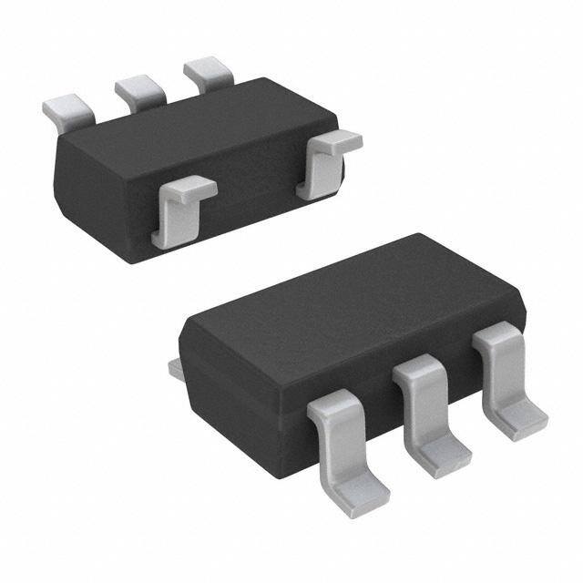
| 描述 | IC VOLT DETECTOR ADJ/1.5V SC70-5监控电路 Adj 1.5V V Detector |
| 产品分类 | |
| 品牌 | Texas Instruments |
| 产品手册 | |
| 产品图片 |
|
| rohs | 符合RoHS无铅 / 符合限制有害物质指令(RoHS)规范要求 |
| 产品系列 | 电源管理 IC,监控电路,Texas Instruments TPS3803G15DCKR- |
| NumberofInputsMonitored | 1 Input |
| 数据手册 | |
| 产品型号 | TPS3803G15DCKR |
| 产品种类 | 监控电路 |
| 人工复位 | No Manual Reset |
| 供应商器件封装 | SC-70-5 |
| 其它名称 | 296-13406-6 |
| 准确性 | +/- 1.5 % |
| 包装 | Digi-Reel® |
| 单位重量 | 2.500 mg |
| 受监控电压数 | 1 |
| 商标 | Texas Instruments |
| 复位 | 低有效 |
| 复位超时 | 标准传输延迟为 5 µs |
| 安装类型 | 表面贴装 |
| 安装风格 | SMD/SMT |
| 封装 | Reel |
| 封装/外壳 | 6-TSSOP(5 引线),SC-88A,SOT-353 |
| 封装/箱体 | SC-70-5 |
| 工作温度 | -40°C ~ 85°C |
| 工作电源电流 | 3 uA |
| 工厂包装数量 | 3000 |
| 最大工作温度 | + 125 C |
| 最小工作温度 | - 40 C |
| 标准包装 | 1 |
| 欠电压阈值 | 1.4 V |
| 电压-阈值 | 1.4V |
| 电池备用开关 | No Backup |
| 电源电压-最大 | 6 V |
| 电源电压-最小 | 1.3 V |
| 监视器 | No Watchdog |
| 类型 | 简单复位/加电复位 |
| 系列 | TPS3803G15 |
| 被监测输入数 | 1 Input |
| 输出 | 开路漏极或开路集电极 |
| 输出类型 | Open Drain |
| 重置延迟时间 | 5.5 us |
| 阈值电压 | 1.226 V |


- 商务部:美国ITC正式对集成电路等产品启动337调查
- 曝三星4nm工艺存在良率问题 高通将骁龙8 Gen1或转产台积电
- 太阳诱电将投资9.5亿元在常州建新厂生产MLCC 预计2023年完工
- 英特尔发布欧洲新工厂建设计划 深化IDM 2.0 战略
- 台积电先进制程称霸业界 有大客户加持明年业绩稳了
- 达到5530亿美元!SIA预计今年全球半导体销售额将创下新高
- 英特尔拟将自动驾驶子公司Mobileye上市 估值或超500亿美元
- 三星加码芯片和SET,合并消费电子和移动部门,撤换高东真等 CEO
- 三星电子宣布重大人事变动 还合并消费电子和移动部门
- 海关总署:前11个月进口集成电路产品价值2.52万亿元 增长14.8%


PDF Datasheet 数据手册内容提取
TPS3803−01 TPS3803G15 TPS3805H33 www.ti.com SLVS392A − JULY 2001 − REVISED JUNE 2007 VOLTAGE DETECTOR FEATURES APPLICATIONS (cid:1) (cid:1) Single Voltage Detector (TPS3803): Applications Using DSPs, Microcontrollers, Adjustable/1.5 V or Microprocessors (cid:1) (cid:1) Dual Voltage Detector (TPS3805): Wireless Communication Systems Adjustable/3.3 V (cid:1) Portable/Battery-Powered Equipment (cid:1) High ±1.5% Threshold Voltage Accuracy (cid:1) Programmable Controls (cid:1) Supply Current: 3 µA Typical at V = 3.3 V (cid:1) DD Intelligent Instruments (cid:1) Push/Pull Reset Output (TPS3805) Open-Drain (cid:1) Industrial Equipment Reset Output (TPS3803) (cid:1) Notebook/Desktop Computers (cid:1) Temperature Range: −40°C to +85°C (cid:1) Automotive Systems (cid:1) 5-Pin SC−70 Package DCKPACKAGE DESCRIPTION (TopView) TPS3803−01,TPS3803G15,TPS3805 The TPS3803 and TPS3805 families of supervisory NC 1 5 SENSE circuits provide circuit initialization and timing supervision, NC(1) primarily for DSPs and processor-based systems. GND 2 The TPS3803G15 device has a fixed-sense threshold voltage VIT set by an internal voltage divider, whereas the RESET 3 4 VDD TPS3803−01 has an adjustable SENSE input that can be configured by two external resistors. In addition to the fixed (1)NC= NoConnectiononTPS3803G15 sense threshold monitored at V , the TPS3805 devices DD provide a second adjustable SENSE input. RESET is TypicalOperatingCircuit asserted in case any of the two voltages drops below V IT. 1.6V 3.3 V During power on, RESET is asserted when supply voltage V becomes higher than 0.8 V. Thereafter, the DD supervisory circuit monitors VDD (and/or SENSE) and DVDD CVDD keeps RESET active as long as VDD or SENSE remains R1 V RESET RESET DD below the threshold voltage V . As soon as V (SENSE) IT DD rises above the threshold voltage V , RESET is TPS3805H33 TMS320VC5416 IT deasserted again. The product spectrum is designed for SENSE GND 1.5V, 3.3 V, and adjustable supply voltages. The devices GND R2 are available in a 5-pin SC-70 package. The TPS3803 and TPS3805 devices are characterized for operation over a temperature range of −40°C to +85°C. Please be aware that an important notice concerning availability, standard warranty, and use in critical applications of TexasInstruments semiconductor products and disclaimers thereto appears at the end of this data sheet. All trademarks are the property of their respective owners. (cid:1)(cid:2)(cid:3)(cid:4)(cid:5)(cid:6)(cid:7)(cid:8)(cid:3)(cid:9) (cid:4)(cid:10)(cid:7)(cid:10) (cid:11)(cid:12)(cid:13)(cid:14)(cid:15)(cid:16)(cid:17)(cid:18)(cid:11)(cid:14)(cid:12) (cid:11)(cid:19) (cid:20)(cid:21)(cid:15)(cid:15)(cid:22)(cid:12)(cid:18) (cid:17)(cid:19) (cid:14)(cid:13) (cid:23)(cid:21)(cid:24)(cid:25)(cid:11)(cid:20)(cid:17)(cid:18)(cid:11)(cid:14)(cid:12) (cid:26)(cid:17)(cid:18)(cid:22)(cid:27) (cid:1)(cid:15)(cid:14)(cid:26)(cid:21)(cid:20)(cid:18)(cid:19) Copyright 2001−2007, Texas Instruments Incorporated (cid:20)(cid:14)(cid:12)(cid:13)(cid:14)(cid:15)(cid:16) (cid:18)(cid:14) (cid:19)(cid:23)(cid:22)(cid:20)(cid:11)(cid:13)(cid:11)(cid:20)(cid:17)(cid:18)(cid:11)(cid:14)(cid:12)(cid:19) (cid:23)(cid:22)(cid:15) (cid:18)(cid:28)(cid:22) (cid:18)(cid:22)(cid:15)(cid:16)(cid:19) (cid:14)(cid:13) (cid:7)(cid:22)(cid:29)(cid:17)(cid:19) (cid:8)(cid:12)(cid:19)(cid:18)(cid:15)(cid:21)(cid:16)(cid:22)(cid:12)(cid:18)(cid:19) (cid:19)(cid:18)(cid:17)(cid:12)(cid:26)(cid:17)(cid:15)(cid:26) (cid:30)(cid:17)(cid:15)(cid:15)(cid:17)(cid:12)(cid:18)(cid:31)(cid:27) (cid:1)(cid:15)(cid:14)(cid:26)(cid:21)(cid:20)(cid:18)(cid:11)(cid:14)(cid:12) (cid:23)(cid:15)(cid:14)(cid:20)(cid:22)(cid:19)(cid:19)(cid:11)(cid:12)! (cid:26)(cid:14)(cid:22)(cid:19) (cid:12)(cid:14)(cid:18) (cid:12)(cid:22)(cid:20)(cid:22)(cid:19)(cid:19)(cid:17)(cid:15)(cid:11)(cid:25)(cid:31) (cid:11)(cid:12)(cid:20)(cid:25)(cid:21)(cid:26)(cid:22) (cid:18)(cid:22)(cid:19)(cid:18)(cid:11)(cid:12)! (cid:14)(cid:13) (cid:17)(cid:25)(cid:25) (cid:23)(cid:17)(cid:15)(cid:17)(cid:16)(cid:22)(cid:18)(cid:22)(cid:15)(cid:19)(cid:27) www.ti.com
(cid:7)(cid:1)"#$%#&%’ (cid:7)(cid:1)"#$%#(’) (cid:7)(cid:1)"#$%)*## www.ti.com SLVS392A − JULY 2001 − REVISED JUNE 2007 This integrated circuit can be damaged by ESD. Texas Instruments recommends that all integrated circuits be handled with appropriate precautions. Failure to observe proper handling and installation procedures can cause damage. ESD damage can range from subtle performance degradation to complete device failure. Precision integrated circuits may be more susceptible to damage because very small parametric changes could cause the device not to meet its published specifications. PACKAGE INFORMATION THRESHOLD VOLTAGE TTAA DDEEVVIICCEE NNAAMMEE MMAARRKKIINNGG VDD SENSE TPS3803−01DCKR(1) NA 1.226 V AWG −−4400(cid:2)CC ttoo ++8855(cid:2)CC TPS3803G15DCKR(1) 1.40 V NA AWI TPS3805H33DCKR(1) 3.05 V 1.226 V AWK (1)The DCKR passive indicates tape and reel containing 3000 parts. ORDERING INFORMATION TPS380 3 G 15 DCK R Reel Package Nominal Supply Voltage Nominal Threshold Voltage Functionality Family Function/Truth Tables TPS3803-01 TPS3803G15 SENSE > VIT RESET VDD > VIT RESET 0 L 0 L 1 H 1 H TPS3805H33 VDD > VIT SENSE > VIT RESET 0 0 L 0 1 L 1 0 L 1 1 H 2
(cid:7)(cid:1)"#$%#&%’ (cid:7)(cid:1)"#$%#(’) (cid:7)(cid:1)"#$%)*## www.ti.com SLVS392A − JULY 2001 − REVISED JUNE 2007 FUNCTIONAL BLOCK DIAGRAM TPS3803G15 TPS3803−01 Device VDD SupplyVoltage R1 RESET VDD _ _ RESET SENSE + R2 + GND GND Reference Reference Voltage Voltage of1.215V of1.226V TPS3805 _ SENSE + RESET R1 _ VDD + R2 GND Reference Voltage of1.226V 3
(cid:7)(cid:1)"#$%#&%’ (cid:7)(cid:1)"#$%#(’) (cid:7)(cid:1)"#$%)*## www.ti.com SLVS392A − JULY 2001 − REVISED JUNE 2007 TIMING REQUIREMENTS VDD or SENSE VIT + Vhys VIT 0.8 V RESET = Undefined Terminal Functions TERMINAL II//OO DDEESSCCRRIIPPTTIIOONN NAME NO. GND 2 I Ground RESET 3 O Active-low reset output (TPS3803—open−drain, TPS3805—push/pull) SENSE 5 I Adjustable sense input NC 1 No internal connection NC (TPS3803G15) 5 No internal connection VDD 4 I Input supply voltage, fixed sense input for TPS3803G15 and TPS3805 4
(cid:7)(cid:1)"#$%#&%’ (cid:7)(cid:1)"#$%#(’) (cid:7)(cid:1)"#$%)*## www.ti.com SLVS392A − JULY 2001 − REVISED JUNE 2007 ABSOLUTE MAXIMUM RATINGS(1) Over operating free-air temperature range, unless otherwise noted. Supply voltage, V (2) . . . . . . . . . . . . . . . . . . . . . . . . . . . . . . . . . . . . . . . . . . . . . . . . . . . . . . . . . . . . . . . . . . . . . . +7 V DD All other pins(2) . . . . . . . . . . . . . . . . . . . . . . . . . . . . . . . . . . . . . . . . . . . . . . . . . . . . . . . . . . . . . . . . . . . . −0.3 V to +7 V Maximum low-output current, I . . . . . . . . . . . . . . . . . . . . . . . . . . . . . . . . . . . . . . . . . . . . . . . . . . . . . . . . . . . +5 mA OL Maximum high-output current, I . . . . . . . . . . . . . . . . . . . . . . . . . . . . . . . . . . . . . . . . . . . . . . . . . . . . . . . . . . −5 mA OH Input clamp current, IIK (VI < 0 or VI > VDD) . . . . . . . . . . . . . . . . . . . . . . . . . . . . . . . . . . . . . . . . . . . . . . . . . ±10 mA Output clamp current, IOK (VO < 0 or VO > VDD) . . . . . . . . . . . . . . . . . . . . . . . . . . . . . . . . . . . . . . . . . . . . ±10 mA Continuous total power dissipation . . . . . . . . . . . . . . . . . . . . . . . . . . . . . . . . . . . . . . See Dissipation Rating Table Operating free-air temperature range, T . . . . . . . . . . . . . . . . . . . . . . . . . . . . . . . . . . . . . . . . . . . . −40°C to +85°C A Storage temperature range, T . . . . . . . . . . . . . . . . . . . . . . . . . . . . . . . . . . . . . . . . . . . . . . . . . . . −65°C to +150°C stg Soldering temperature . . . . . . . . . . . . . . . . . . . . . . . . . . . . . . . . . . . . . . . . . . . . . . . . . . . . . . . . . . . . . . . . . . . +260°C (1)Stresses beyond those listed under “absolute maximum ratings” may cause permanent damage to the device. These are stress ratings only, and functional operation of the device at these or any other conditions beyond those indicated under “recommended operating conditions” is not implied. Exposure to absolute−maximum−rated conditions for extended periods may affect device reliability. (2)All voltage values are with respect to GND. For reliable operation the device should not be continuously operated at 7 V for more than t = 1000 h. DISSIPATION RATING TABLE PACKAGE TA < +25°C DERATING FACTOR TA = +70°C TA = +85°C POWER RATING ABOVE TA = +25°C POWER RATING POWER RATING DCK 321 mW 2.6 mW/°C 206 mW 167 mW RECOMMENDED OPERATING CONDITIONS MIN MAX UNIT Supply voltage, VDD 1.3 6 V Input voltage, VI 0 VDD + 0.3 V Operating free-air temperature range, TA −40 85 °C 5
(cid:7)(cid:1)"#$%#&%’ (cid:7)(cid:1)"#$%#(’) (cid:7)(cid:1)"#$%)*## www.ti.com SLVS392A − JULY 2001 − REVISED JUNE 2007 ELECTRICAL CHARACTERISTICS Over recommended operating free-air temperature range, unless otherwise noted. PARAMETER TEST CONDITIONS MIN TYP MAX UNIT VDD = 1.5 V, IOH = −0.5 mA VVOOHH HHiigghh--lleevveell oouuttppuutt vvoollttaaggee ((TTPPSS33880055 oonnllyy)) VDD = 3.3 V, IOH = −1.0 mA 00..88 xx VVDDDD VV VDD = 6 V, IOH = −1.5 mA VDD = 1.5 V, IOL = 1.0 mA VVOOLL LLooww--lleevveell oouuttppuutt vvoollttaaggee VDD = 3.3 V, IOL = 2 mA 00..33 VV VDD = 6 V, IOL = 3 mA VIT > 1.5 V, TA = 25°C 0.8 V PPoowweerr--uupp rreesseett vvoollttaaggee((11)) VIT ≤ 1.5 V, TA = 25°C 1.0 V SENSE 1.208 1.226 1.244 NNeeggaattiivvee--ggooiinngg iinnppuutt tthhrreesshhoolldd VVIITT vvoollttaaggee((22)) TPS3803G15 TTAA == −−4400°CC ttoo ++8855°CC 1.379 1.4 1.421 VV TPS3805H33 3.004 3.05 3.096 1.2 V < VIT < 2.5 V 15 VVhhyyss HHyysstteerreessiiss 2.5 V < VIT < 3.5 V 30 mmVV II Input current SENSE −25 25 nA IOH High-level output current at RESET Open drain only VDD = VIT + 0.2V, VOH = VDD 300 nA TPS3803−01 2 4 TPS3805, VDD = 3.3 V, output unconnected 3 5 TPS3803G15 IIDDDD SSuuppppllyy ccuurrrreenntt µAA TPS3803−01 2 4 TPS3805, VDD = 6 V, output unconnected 4 6 TPS3803G15 CI Input capacitance VI = 0 V to VDD 1 pF (1)The lowest supply voltage at which RESET (VOL(max) = 0.2 V, IOL = 50 µA) becomes active. tr(VDD) ≥15 µs/V. (2)To ensure the best stability of the threshold voltage, place a bypass capacitor (ceramic, 0.1 µF) near the supply terminals. TIMING REQUIREMENTS AT RL = 1 MΩ, CL = 50 PF, TA = −40°C TO +85°C. PARAMETER TEST CONDITIONS MIN TYP MAX UNIT At VDD ttww PPuullssee wwiiddtthh VVIIHH == 11..0055 xx VVIITT,, VVIILL == 00..9955 xx VVIITT 55..55 µss At SENSE SWITCHING CHARACTERISTICS AT RL = 1 MΩ, CL = 50 PF, TA = −40°C TO +85°C. PARAMETER TEST CONDITIONS MIN TYP MAX UNIT PPrrooppaaggaattiioonn ((ddeellaayy)) ttiimmee,, VDD to RESET delay ttPPHHLL high-to-low-level output SENSE to RESET delay VVIIHH == 11..0055 xx VVIITT,, 55 110000 VVIILL == 00..9955 xx VVIITT µss PPrrooppaaggaattiioonn ((ddeellaayy)) ttiimmee,, VDD to RESET delay ttPPLLHH low-to-high-level output SENSE to RESET delay 55 110000 6
(cid:7)(cid:1)"#$%#&%’ (cid:7)(cid:1)"#$%#(’) (cid:7)(cid:1)"#$%)*## www.ti.com SLVS392A − JULY 2001 − REVISED JUNE 2007 TYPICAL CHARACTERISTICS TPS3805H33 TPS3803−01 SUPPLY CURRENT SUPPLY CURRENT vs vs SUPPLY VOLTAGE SUPPLY VOLTAGE 6 3 SENSE = GND RESET = Open 5 2.5 A A µ µ − 4 − 2 nt nt e e r r r r u u ply C 3 85°C ply C 1.5 85°C p p u u S 2 25°C S 1 25°C − − DD 0°C DD 0°C I −40°C I 1 0.5 −40°C SENSE = GND RESET = Open 0 0 0 0.5 1 1.5 2 2.5 3 3.5 4 4.5 5 5.5 6 0 0.5 1 1.5 2 2.5 3 3.5 4 4.5 5 5.5 6 VDD − Supply Voltage − V VDD − Supply Voltage − V Figure 1 Figure 2 LOW-LEVEL OUTPUT VOLTAGE LOW-LEVEL OUTPUT VOLTAGE vs vs LOW-LEVEL OUTPUT CURRENT LOW-LEVEL OUTPUT CURRENT 1.60 0.50 (Expanded View) VDD = 1.5 V 0.45 VDD = 1.5 V V 1.40 V(SENSE) = Low V V(SENSE) = Low − − 0.40 ge 1.20 ge 85°C Volta 85°C Volta 0.35 25°C put 1.00 25°C put 0.30 0°C ut ut el O 0.80 0°C el O 0.25 −40°C v v e e 0.20 L 0.60 −40°C L w- w- o o 0.15 L L − 0.40 − L L 0.10 O O V V 0.20 0.05 0 0 0 1 2 3 4 5 0 0.5 1 1.5 2 2.5 3 IOL − Low-Level Output Current − mA IOL − Low-Level Output Current − mA Figure 3 Figure 4 7
(cid:7)(cid:1)"#$%#&%’ (cid:7)(cid:1)"#$%#(’) (cid:7)(cid:1)"#$%)*## www.ti.com SLVS392A − JULY 2001 − REVISED JUNE 2007 TYPICAL CHARACTERISTICS (continued) LOW-LEVEL OUTPUT VOLTAGE LOW-LEVEL OUTPUT VOLTAGE vs vs LOW-LEVEL OUTPUT CURRENT LOW-LEVEL OUTPUT CURRENT 3.5 1 VDD = 6 V VDD = 6 V 0.9 V(SENSE) = Low 3 V(SENSE) = Low V V − 0.8 85°C oltage − 2.5 25°C85°C Voltage 0.7 0°C25°C ut V 2 0°C put 0.6 −40°C utp Out 0.5 vel O 1.5 −40°C evel 0.4 e L w-L ow- 0.3 o 1 L L − − L 0.2 (Expanded View) L O VO 0.5 V 0.1 0 0 0 5 10 15 20 25 30 35 40 45 50 0 2 4 6 8 10 12 14 16 18 20 IOL − Low-Level Output Current − mA IOL − Low-Level Output Current − mA Figure 5 Figure 6 TPS3805H33 TPS3805H33 HIGH-LEVEL OUTPUT VOLTAGE HIGH-LEVEL OUTPUT VOLTAGE vs vs HIGH-LEVEL OUTPUT CURRENT HIGH-LEVEL OUTPUT CURRENT 3.5 3.3 VDD = 3.3 V VDD = 3.3 V V 3.25 V(SENSE) = High V 3.2 V(SENSE) = High − − ge 3 ge 3.1 a a olt olt V V put 2.75 85°C put 3 85°C ut ut O 2.5 O 2.9 25°C vel 25°C vel Le 2.25 Le 2.8 0°C gh- 0°C gh- −40°C − Hi 2 −40°C − Hi 2.7 H H O O V 1.75 V 2.6 (Expanded View) 1.5 2.5 −14 −12 −10 −8 −6 −4 −2 0 −5 −4 −3 −2 −1 0 IOH − High-Level Output Current − mA IOH − High-Level Output Current − mA Figure 7 Figure 8 8
(cid:7)(cid:1)"#$%#&%’ (cid:7)(cid:1)"#$%#(’) (cid:7)(cid:1)"#$%)*## www.ti.com SLVS392A − JULY 2001 − REVISED JUNE 2007 TYPICAL CHARACTERISTICS (continued) TPS3805H33 TPS3805H33 HIGH-LEVEL OUTPUT VOLTAGE HIGH-LEVEL OUTPUT VOLTAGE vs vs HIGH-LEVEL OUTPUT CURRENT HIGH-LEVEL OUTPUT CURRENT 6 6 VDD = 6 V V(SENSE) = High VDD = 6 V ge − V 5.5 ge − V 5.8 V(SENSE) = High Volta 5 Volta 5.6 ut ut utp 85°C utp 5.4 85°C O 4.5 O gh-Level 4 25°C gh-Level 5.2 −40°C02°C5°C − Hi 0°C − Hi 5 H H O 3.5 O V −40°C V 4.8 (Expanded View) 3 4.6 −4 −3 −2 −1 0 −14 −12 −10 −8 −6 −4 −2 0 IOH − High-Level Output Current − mA IOH − High-Level Output Current − mA Figure 9 Figure 10 TPS3803−01 NORMALIZED INPUT THRESHOLD VOLTAGE MINIMUM PULSE DURATION AT V DD vs vs C) FREE-AIR TEMPERATURE AT SENSE VDD THRESHOLD OVERDRIVE VOLTAGE ° 5 21.0020 10 (T VI V(T) / ITA11..00001105 VRDEDSE =T 6 = V 100 kΩ to VDD µV − sDD 89 ge at 7 a n Volt1.0005 atio 6 old 1.0000 Dur 5 nput Thresh0.9995 mum Pulse 43 ed I0.9990 Mini 2 maliz0.9985 − w 1 r t o N − T0.9980−40 −20 0 20 40 60 80 00 0.1 0.2 0.3 0.4 0.5 0.6 0.7 0.8 0.9 1 VI TA − Free-Air Temperature at SENSE − °C VDD − Threshold Overdrive Voltage − V Figure 11 Figure 12 9
(cid:7)(cid:1)"#$%#&%’ (cid:7)(cid:1)"#$%#(’) (cid:7)(cid:1)"#$%)*## www.ti.com SLVS392A − JULY 2001 − REVISED JUNE 2007 TYPICAL CHARACTERISTICS (continued) MINIMUM PULSE DURATION AT SENSE vs SENSE THRESHOLD OVERDRIVE VOLTAGE 10 s µ 9 − E S 8 N E S 7 at n o 6 ati r u 5 D e s ul 4 P m 3 u m ni 2 Mi − w 1 t 0 0 0.1 0.2 0.3 0.4 0.5 0.6 0.7 0.8 0.9 1 SENSE − Threshold Overdrive Voltage − V Figure 13 10
Revision History DATE REV PAGE SECTION DESCRIPTION Front Page — Updated front page. 66//0077 AA 3 — Functional block diagram change. NOTE: Page numbers for previous revisions may differ from page numbers in the current version.
PACKAGE OPTION ADDENDUM www.ti.com 6-Feb-2020 PACKAGING INFORMATION Orderable Device Status Package Type Package Pins Package Eco Plan Lead/Ball Finish MSL Peak Temp Op Temp (°C) Device Marking Samples (1) Drawing Qty (2) (6) (3) (4/5) TPS3803-01DCKR ACTIVE SC70 DCK 5 3000 Green (RoHS NIPDAU | NIPDAUAG Level-1-260C-UNLIM -40 to 85 AWG & no Sb/Br) TPS3803-01DCKRG4 ACTIVE SC70 DCK 5 3000 Green (RoHS NIPDAU Level-1-260C-UNLIM -40 to 85 AWG & no Sb/Br) TPS3803G15DCKR ACTIVE SC70 DCK 5 3000 Green (RoHS NIPDAUAG Level-1-260C-UNLIM AWI & no Sb/Br) TPS3805H33DCKR ACTIVE SC70 DCK 5 3000 Green (RoHS NIPDAU | NIPDAUAG Level-1-260C-UNLIM -40 to 85 AWK & no Sb/Br) TPS3805H33DCKRG4 ACTIVE SC70 DCK 5 3000 Green (RoHS NIPDAU Level-1-260C-UNLIM -40 to 85 AWK & no Sb/Br) (1) The marketing status values are defined as follows: ACTIVE: Product device recommended for new designs. LIFEBUY: TI has announced that the device will be discontinued, and a lifetime-buy period is in effect. NRND: Not recommended for new designs. Device is in production to support existing customers, but TI does not recommend using this part in a new design. PREVIEW: Device has been announced but is not in production. Samples may or may not be available. OBSOLETE: TI has discontinued the production of the device. (2) RoHS: TI defines "RoHS" to mean semiconductor products that are compliant with the current EU RoHS requirements for all 10 RoHS substances, including the requirement that RoHS substance do not exceed 0.1% by weight in homogeneous materials. Where designed to be soldered at high temperatures, "RoHS" products are suitable for use in specified lead-free processes. TI may reference these types of products as "Pb-Free". RoHS Exempt: TI defines "RoHS Exempt" to mean products that contain lead but are compliant with EU RoHS pursuant to a specific EU RoHS exemption. Green: TI defines "Green" to mean the content of Chlorine (Cl) and Bromine (Br) based flame retardants meet JS709B low halogen requirements of <=1000ppm threshold. Antimony trioxide based flame retardants must also meet the <=1000ppm threshold requirement. (3) MSL, Peak Temp. - The Moisture Sensitivity Level rating according to the JEDEC industry standard classifications, and peak solder temperature. (4) There may be additional marking, which relates to the logo, the lot trace code information, or the environmental category on the device. (5) Multiple Device Markings will be inside parentheses. Only one Device Marking contained in parentheses and separated by a "~" will appear on a device. If a line is indented then it is a continuation of the previous line and the two combined represent the entire Device Marking for that device. (6) Lead/Ball Finish - Orderable Devices may have multiple material finish options. Finish options are separated by a vertical ruled line. Lead/Ball Finish values may wrap to two lines if the finish value exceeds the maximum column width. Addendum-Page 1
PACKAGE OPTION ADDENDUM www.ti.com 6-Feb-2020 Important Information and Disclaimer:The information provided on this page represents TI's knowledge and belief as of the date that it is provided. TI bases its knowledge and belief on information provided by third parties, and makes no representation or warranty as to the accuracy of such information. Efforts are underway to better integrate information from third parties. TI has taken and continues to take reasonable steps to provide representative and accurate information but may not have conducted destructive testing or chemical analysis on incoming materials and chemicals. TI and TI suppliers consider certain information to be proprietary, and thus CAS numbers and other limited information may not be available for release. In no event shall TI's liability arising out of such information exceed the total purchase price of the TI part(s) at issue in this document sold by TI to Customer on an annual basis. OTHER QUALIFIED VERSIONS OF TPS3803, TPS3805H33 : •Automotive: TPS3803-Q1, TPS3805H33-Q1 •Enhanced Product: TPS3803-EP, TPS3805H33-EP NOTE: Qualified Version Definitions: •Automotive - Q100 devices qualified for high-reliability automotive applications targeting zero defects •Enhanced Product - Supports Defense, Aerospace and Medical Applications Addendum-Page 2
PACKAGE MATERIALS INFORMATION www.ti.com 23-Apr-2020 TAPE AND REEL INFORMATION *Alldimensionsarenominal Device Package Package Pins SPQ Reel Reel A0 B0 K0 P1 W Pin1 Type Drawing Diameter Width (mm) (mm) (mm) (mm) (mm) Quadrant (mm) W1(mm) TPS3803-01DCKR SC70 DCK 5 3000 180.0 8.4 2.41 2.41 1.2 4.0 8.0 Q3 TPS3803G15DCKR SC70 DCK 5 3000 180.0 8.4 2.41 2.41 1.2 4.0 8.0 Q3 TPS3805H33DCKR SC70 DCK 5 3000 180.0 8.4 2.41 2.41 1.2 4.0 8.0 Q3 PackMaterials-Page1
PACKAGE MATERIALS INFORMATION www.ti.com 23-Apr-2020 *Alldimensionsarenominal Device PackageType PackageDrawing Pins SPQ Length(mm) Width(mm) Height(mm) TPS3803-01DCKR SC70 DCK 5 3000 183.0 183.0 20.0 TPS3803G15DCKR SC70 DCK 5 3000 183.0 183.0 20.0 TPS3805H33DCKR SC70 DCK 5 3000 183.0 183.0 20.0 PackMaterials-Page2
None
None
IMPORTANTNOTICEANDDISCLAIMER TI PROVIDES TECHNICAL AND RELIABILITY DATA (INCLUDING DATASHEETS), DESIGN RESOURCES (INCLUDING REFERENCE DESIGNS), APPLICATION OR OTHER DESIGN ADVICE, WEB TOOLS, SAFETY INFORMATION, AND OTHER RESOURCES “AS IS” AND WITH ALL FAULTS, AND DISCLAIMS ALL WARRANTIES, EXPRESS AND IMPLIED, INCLUDING WITHOUT LIMITATION ANY IMPLIED WARRANTIES OF MERCHANTABILITY, FITNESS FOR A PARTICULAR PURPOSE OR NON-INFRINGEMENT OF THIRD PARTY INTELLECTUAL PROPERTY RIGHTS. These resources are intended for skilled developers designing with TI products. You are solely responsible for (1) selecting the appropriate TI products for your application, (2) designing, validating and testing your application, and (3) ensuring your application meets applicable standards, and any other safety, security, or other requirements. These resources are subject to change without notice. TI grants you permission to use these resources only for development of an application that uses the TI products described in the resource. Other reproduction and display of these resources is prohibited. No license is granted to any other TI intellectual property right or to any third party intellectual property right. TI disclaims responsibility for, and you will fully indemnify TI and its representatives against, any claims, damages, costs, losses, and liabilities arising out of your use of these resources. TI’s products are provided subject to TI’s Terms of Sale (www.ti.com/legal/termsofsale.html) or other applicable terms available either on ti.com or provided in conjunction with such TI products. TI’s provision of these resources does not expand or otherwise alter TI’s applicable warranties or warranty disclaimers for TI products. Mailing Address: Texas Instruments, Post Office Box 655303, Dallas, Texas 75265 Copyright © 2020, Texas Instruments Incorporated