ICGOO在线商城 > 集成电路(IC) > PMIC - 监控器 > TPS3620-33MDGKREP
 Datasheet下载
- 型号: TPS3620-33MDGKREP
- 制造商: Texas Instruments
- 库位|库存: xxxx|xxxx
- 要求:
| 数量阶梯 | 香港交货 | 国内含税 |
| +xxxx | $xxxx | ¥xxxx |
查看当月历史价格
查看今年历史价格
TPS3620-33MDGKREP产品简介:
ICGOO电子元器件商城为您提供TPS3620-33MDGKREP由Texas Instruments设计生产,在icgoo商城现货销售,并且可以通过原厂、代理商等渠道进行代购。 TPS3620-33MDGKREP价格参考¥34.32-¥56.35。Texas InstrumentsTPS3620-33MDGKREP封装/规格:PMIC - 监控器, 推挽式,图腾柱 监控器 1 通道 8-VSSOP。您可以下载TPS3620-33MDGKREP参考资料、Datasheet数据手册功能说明书,资料中有TPS3620-33MDGKREP 详细功能的应用电路图电压和使用方法及教程。
TPS3620-33MDGKREP 是由 Texas Instruments(德州仪器)生产的一款 PMIC - 监控器芯片,属于电压监控器系列。其主要应用场景包括但不限于以下领域:

1. 电源监控与保护
   TPS3620-33MDGKREP 可用于监测系统中的电源电压,确保设备在安全的工作电压范围内运行。当检测到电压低于预设阈值(如 3.3V)时,会触发复位信号以保护系统硬件。它适用于需要高可靠性和稳定性的电源管理场景。

2. 嵌入式系统
   在微控制器、DSP 或 FPGA 等嵌入式系统中,该芯片可以监控核心供电电压,防止因电压波动导致的系统崩溃或数据丢失。它支持快速响应,确保系统在异常情况下能够及时复位并恢复正常运行。

3. 消费电子设备
   包括智能手机、平板电脑、笔记本电脑和其他便携式设备,TPS3620-33MDGKREP 可用于电池管理系统中,监控电池电压状态,并在电压过低时触发警告或关机操作,从而延长电池寿命。

4. 工业自动化
   在工业控制领域,该器件可用于 PLC(可编程逻辑控制器)、传感器模块和通信接口中,提供实时电压监控功能,避免因电压不稳定引起的设备故障或数据错误。

5. 通信设备
   对于路由器、交换机或其他网络设备,TPS3620-33MDGKREP 能够保障关键组件的供电稳定性,确保通信链路的连续性和可靠性。

6. 汽车电子
   在汽车电子系统中,例如车载信息娱乐系统、导航设备或发动机控制单元(ECU),该芯片可用于监控车载电源电压,确保电子模块正常工作,同时满足汽车行业对可靠性和耐用性的严格要求。

7. 医疗设备
   在便携式或固定式医疗设备中,如监护仪、血糖仪等,TPS3620-33MDGKREP 提供精准的电压监控功能,保证设备测量结果的准确性和患者安全。

总结来说,TPS3620-33MDGKREP 的典型应用场景集中在需要精确电压监控和保护的领域,特别是在对稳定性、可靠性和功耗有较高要求的系统中表现尤为突出。
| 参数 | 数值 |
| 产品目录 | 集成电路 (IC) |
| 描述 | IC BACKUP-BATT SUPERVISOR 8VSSOP |
| 产品分类 | |
| 品牌 | Texas Instruments |
| 数据手册 | |
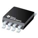
| 产品图片 |
|
| 产品型号 | TPS3620-33MDGKREP |
| rohs | 无铅 / 符合限制有害物质指令(RoHS)规范要求 |
| 产品系列 | - |
| 产品目录页面 | |
| 供应商器件封装 | 8-VSSOP |
| 其它名称 | 296-22437-1 |
| 包装 | 剪切带 (CT) |
| 受监控电压数 | 1 |
| 复位 | 低有效 |
| 复位超时 | 最小为 60 ms |
| 安装类型 | 表面贴装 |
| 封装/外壳 | 8-TSSOP,8-MSOP(0.118",3.00mm 宽) |
| 工作温度 | -55°C ~ 125°C |
| 标准包装 | 1 |
| 电压-阈值 | 2.93V |
| 类型 | 备用电池电路 |
| 输出 | 推挽式,图腾柱 |


- 商务部:美国ITC正式对集成电路等产品启动337调查
- 曝三星4nm工艺存在良率问题 高通将骁龙8 Gen1或转产台积电
- 太阳诱电将投资9.5亿元在常州建新厂生产MLCC 预计2023年完工
- 英特尔发布欧洲新工厂建设计划 深化IDM 2.0 战略
- 台积电先进制程称霸业界 有大客户加持明年业绩稳了
- 达到5530亿美元!SIA预计今年全球半导体销售额将创下新高
- 英特尔拟将自动驾驶子公司Mobileye上市 估值或超500亿美元
- 三星加码芯片和SET,合并消费电子和移动部门,撤换高东真等 CEO
- 三星电子宣布重大人事变动 还合并消费电子和移动部门
- 海关总署:前11个月进口集成电路产品价值2.52万亿元 增长14.8%


PDF Datasheet 数据手册内容提取
TPS3619-33-EP, TPS3619-50-EP TPS3620-33-EP, TPS3620-50-EP www.ti.com SGLS350C–JULY2006–REVISEDSEPTEMBER2010 BACKUP-BATTERY SUPERVISORS FOR RAM RETENTION CheckforSamples:TPS3619-33-EP,TPS3619-50-EP,TPS3620-33-EP,TPS3620-50-EP FEATURES APPLICATIONS 1 • SupplyCurrentof40mA(Max) • FaxMachines • Battery-SupplyCurrentof100nA(Max) • Set-TopBoxes • PrecisionSupply-VoltageMonitor3.3V,5V, • AdvancedVoice-MailSystems andOtherOptionsonRequest • PortableBattery-PoweredEquipment • Backup-BatteryVoltageCanExceedV • ComputerEquipment DD • AdvancedModems • Power-OnResetGeneratorwithFixed100-ms ResetDelayTime • AutomotiveSystems • PortableLong-TimeMonitoringEquipment • VoltageMonitorforPower-FailorLow-Battery Monitoring • Point-of-SaleEquipment • BatteryFreshnessSeal(TPS3619) DESCRIPTION • Pin-to-PinCompatibleWithMAX819,MAX703, andMAX704 The TPS3619 and TPS3620 families of supervisory circuits monitor and control processor activity by • 8-PinMiniSmall-OutlinePackage(MSOP) providing backup-battery switchover for data retention Package ofCMOSRAM. SUPPORTS DEFENSE, AEROSPACE, During power on, RESET is asserted when the AND MEDICAL APPLICATIONS supplyvoltage(VDDorVBAT)becomeshigherthan1.1 V. Thereafter, the supply voltage supervisor monitors • ControlledBaseline V and keeps RESET output active as long as V DD DD • OneAssembly/TestSite remains below the threshold voltage (V ). An internal IT • OneFabricationSite timer delays the return of the output to the inactive • AvailableinMilitary(–55°C/125°C) state (high) to ensure proper system reset. The delay TemperatureRange(1) time starts after VDD has risen above VIT. When the supply voltage drops below V , the output becomes • ExtendedProductLifeCycle IT active(low)again. • ExtendedProduct-ChangeNotification • ProductTraceability The product spectrum is designed for supply voltages of 3.3 V and 5 V. The TPS3619 and TPS3620 are available in an 8-pin MSOP package and are characterized for operation over a temperature range (1) Additionaltemperaturerangesavailable-contactfactory of–55°Cto125°C. DGK PACKAGE (TOP VIEW) VOUT 1 8 VBAT VDD 2 7 RESET ACTUAL SIZE GND 3 6 MR 3,05 mm x 4,98 mm PFI 4 5 PFO 1 Pleasebeawarethatanimportantnoticeconcerningavailability,standardwarranty,anduseincriticalapplicationsofTexas Instrumentssemiconductorproductsanddisclaimerstheretoappearsattheendofthisdatasheet. PRODUCTIONDATAinformationiscurrentasofpublicationdate. Copyright©2006–2010,TexasInstrumentsIncorporated Products conform to specifications per the terms of the Texas Instruments standard warranty. Production processing does not necessarilyincludetestingofallparameters.
TPS3619-33-EP, TPS3619-50-EP TPS3620-33-EP, TPS3620-50-EP SGLS350C–JULY2006–REVISEDSEPTEMBER2010 www.ti.com This integrated circuit can be damaged by ESD. Texas Instruments recommends that all integrated circuits be handled with appropriateprecautions.Failuretoobserveproperhandlingandinstallationprocedurescancausedamage. ESDdamagecanrangefromsubtleperformancedegradationtocompletedevicefailure.Precisionintegratedcircuitsmaybemore susceptibletodamagebecauseverysmallparametricchangescouldcausethedevicenottomeetitspublishedspecifications. TYPICAL OPERATING CIRCUIT Power TPS3619 Microcontroller Supply 0.1 m F TPS3620 Backup or Battery Microprocessor VDD VBAT External Source RESET RESET Rx PFI PFO I/O Switchover Ry MR Capacitor VOUT 0.1 m F VCC Manual GND GND Reset PACKAGEINFORMATION(1) PACKAGE TRANSPORTMEDIA, T PRODUCT ORDERABLEPARTNUMBER A MARKING QUANTITY TPS3619-33MDGKEP(2) Tube,80 TPS3619-33 BZP TPS3619-33MDGKREP Tapeandreel,2500 TPS3619-50MDGK(2) Tube,80 TPS3619-50 TBD TPS3619-50MDGKREP(2) Tapeandreel,2500 –55°Cto125°C TPS3620-33MDGKTEP Tapeandreel,250 TPS3620-33 BTY TPS3620-33MDGKREP Tapeandreel,2500 TPS3620-50MDGKTEP(2) Tapeandreel,250 TPS3620-50 TBD TPS3620-50MDGKREP(2) Tapeandreel,2500 (1) Forthemostcurrentspecificationsandpackageinformation,seethePackageOptionAddendumlocatedattheendofthisdatasheetor seetheTIwebsiteatwww.ti.com. (2) ProductPreview.Parametersinelectricalcharacteristicsaresubjecttochange. Standard and Application-Specific Versions TPS361 9 33 M DGK R EP DEVICENAME NOMINALVOLTAGE(1),V NOM Designator TPS3619-33DGK 3.3V Reel TPS3619-50DGK 5V Package TPS3620-33DGK 3.3V Temperature Range TPS3620-50DGK 5V Nominal Supply Voltage Functionality (1) Forotherthresholdvoltageversions,contactthelocalTIsales Family officeforavailabilityandleadtime. 2 SubmitDocumentationFeedback Copyright©2006–2010,TexasInstrumentsIncorporated ProductFolderLink(s):TPS3619-33-EPTPS3619-50-EP TPS3620-33-EP TPS3620-50-EP
TPS3619-33-EP, TPS3619-50-EP TPS3620-33-EP, TPS3620-50-EP www.ti.com SGLS350C–JULY2006–REVISEDSEPTEMBER2010 Absolute Maximum Ratings overoperatingfree-airtemperature(unlessotherwisenoted)(1) UNIT V (2) 7V DD Supplyvoltage MRandPFIpins(2) –0.3Vto(V +0.3V) DD V 400mA OUT Continuousoutputcurrent,I O Allotherpins(2) ±10mA Continuoustotalpowerdissipation SeeDissipationRatingsTable Operatingfree-airtemperaturerange,T –55°Cto125°C A Storagetemperaturerange,T –65°Cto150°C stg Leadtemperaturesoldering1,6mm(1/16in)fromcasefor10s 260°C (1) Stressesbeyondthoselistedunderabsolutemaximumratingsmaycausepermanentdamagetothedevice.Thesearestressratings only,andfunctionaloperationofthedeviceattheseoranyotherconditionsbeyondthoseindicatedunderrecommendedoperating conditionsisnotimplied.Exposuretoabsolute-maximum-ratedconditionsforextendedperiodsmayaffectdevicereliability. (2) AllvoltagevaluesarewithrespecttoGND.Forreliableoperation,thedevicemustnotbecontinuouslyoperatedat7Vformorethan t=1000h. Dissipation Ratings T <25°C DERATINGFACTOR T =70°C T =85°C T =125°C PACKAGE A A A A POWERRATING ABOVET =25°C POWERRATING POWERRATING POWERRATING A DGK 470mW 3.76mW/°C 301mW 241mW 93.98mW Recommended Operating Conditions atspecifiedtemperaturerange MIN MAX UNIT V Supplyvoltage 1.65 5.5 V DD V Batterysupplyvoltage 1.5 5.5 V BAT V Inputvoltage 0 V +0.3 V I DD V High-levelinputvoltage 0.7×V V IH DD V Low-levelinputvoltage 0.3×V V IL DD I ContinuousoutputcurrentatV 300 mA O OUT InputtransitionriseandfallrateatMR 100 ns/V Δt/ΔV SlewrateatV orV 1 V/ms DD BAT T Operatingfree-airtemperature –55 125 °C A Copyright©2006–2010,TexasInstrumentsIncorporated SubmitDocumentationFeedback 3 ProductFolderLink(s):TPS3619-33-EPTPS3619-50-EP TPS3620-33-EP TPS3620-50-EP
TPS3619-33-EP, TPS3619-50-EP TPS3620-33-EP, TPS3620-50-EP SGLS350C–JULY2006–REVISEDSEPTEMBER2010 www.ti.com Electrical Characteristics overrecommendedoperatingconditions(unlessotherwisenoted) PARAMETER TESTCONDITIONS MIN TYP MAX UNIT V =3.3V,I =–2mA V –0.4 DD OH DD RESET V =5V,I =–3mA V –0.4 DD OH DD V High-leveloutputvoltage V =1.8V,I =–20mA V –0.3 V OH DD OH DD PFO V =3.3V,I =–80mA V –0.4 DD OH DD V =5V,I =–120mA V –0.4 DD OH DD V =1.8V,I =–400mA 0.2 DD OL V Low-leveloutputvoltage RESET,PFO V =3.3V,I =2mA 0.4 V OL DD OL V =5V,I =3mA 0.4 DD OL V Power-upresetvoltage(1) IOL=20mA,VBAT>1.1Vor 0.4 V res V >1.1V DD I =8.5mA,V =0V, OUT BAT V –50 V =1.8V DD DD I =125mA,V =0V, Normalmode OUT BAT V –150 V =3.3V DD DD V I =190mA,V =0V, mV OUT OUT BAT V –200 V =5V DD DD I =0.5mA,V =1.5V, OUT BAT V –50 Battery-backupmode VDD=0V BAT I =7.5mA,V =3.3V V –150 OUT BAT BAT V toV onresistance V =5V 0.6 1 DD OUT DD r Ω DS(on) V toV onresistance V =3.3V 8 20 BAT OUT DD TPS36XX-33 2.88 2.93 3.05 VIT– Negative-goinginputthreshold TA=–55°Cto125°C V voltage(2) TPS36XX-50 4.46 4.55 4.64 V T =–55°Cto125°C 1.13 1.15 1.185 V PFI A 1.65V<V <2.5V 20 IT V 2.5V<V <3.5V 40 IT IT V Hysteresis 3.5V<V <5.5V 60 mV hys IT PFI 12 VBSW(3) V =1.8V 55 DD I High-levelinputcurrent MR MR=0.7×V , V =5V –30 –76 mA IH DD DD I Low-levelinputcurrent MR MR=0V, V =5V –110 –255 mA IL DD I Inputcurrent PFI –25 25 nA I V =1.8V –0.3 DD I Short-circuitcurrent PFO PFO=0V V =3.3V –1.1 mA OS DD V =5V –2.4 DD V =V 40 OUT DD I V supplycurrent mA DD DD V =V 40 OUT BAT V =V –0.1 0.1 OUT DD I V supplycurrent mA (BAT) BAT V =V 0.5 OUT BAT C Inputcapacitance V =0Vto5V 5 pF I I (1) ThelowestsupplyvoltageatwhichRESETbecomesactive.t ≥15ms/V. r,VDD (2) Toensurethebeststabilityofthethresholdvoltage,abypasscapacitor(ceramic,0.1mF)shouldbeplacednearthesupplyterminals. (3) ForV <1.6V,V switchestoV ,regardlessofV . DD OUT BAT BAT 4 SubmitDocumentationFeedback Copyright©2006–2010,TexasInstrumentsIncorporated ProductFolderLink(s):TPS3619-33-EPTPS3619-50-EP TPS3620-33-EP TPS3620-50-EP
TPS3619-33-EP, TPS3619-50-EP TPS3620-33-EP, TPS3620-50-EP www.ti.com SGLS350C–JULY2006–REVISEDSEPTEMBER2010 Timing Requirements atR =1MΩ,C =50pF,T =25°C L L A PARAMETER TESTCONDITIONS MIN MAX UNIT atV V =V +0.2V,V =V –0.2V 6 ms DD IH IT IL IT t Pulsewidth w atMR V =V +0.2V,V =0.3xV ,V =0.7×V 100 ns DD IT IL DD IH DD Switching Characteristics atR =1MΩ,C =50pF,T =–55°Cto125°C L L A PARAMETER TESTCONDITIONS MIN TYP MAX UNIT V ≥V +0.2V,MR≥0.7×V , t Delaytime DD IT DD 60 100 140 ms d Seetimingdiagram V toRESET V =V –0.4V,V =V +0.4V 2 5 DD IL IT IH IT Propagation(delay)time, PFItoPFOdelay V =V –0.35V,V =V +0.35V 3 5 t IL PFI IH PFI ms PHL high-to-low-leveloutput V ≥V +0.2V,V =0.3×V , MRtoRESET DD IT IL DD 0.1 1 V =0.7×V IH DD TimingDiagram VBAT VIT VDD t VOUT t RESET td td t Copyright©2006–2010,TexasInstrumentsIncorporated SubmitDocumentationFeedback 5 ProductFolderLink(s):TPS3619-33-EPTPS3619-50-EP TPS3620-33-EP TPS3620-50-EP
TPS3619-33-EP, TPS3619-50-EP TPS3620-33-EP, TPS3620-50-EP SGLS350C–JULY2006–REVISEDSEPTEMBER2010 www.ti.com Table1.FUNCTIONTABLE V >V V >V MR V RESET DD IT DD BAT OUT 0 0 L V L BAT 0 0 H V L BAT 0 1 L V L DD 0 1 H V L DD 1 0 L V L DD 1 0 H V H DD 1 1 L V L DD 1 1 H V H DD PFI>V PFO PFI 0 L 1 H CONDITION:V >V (MIN) DD DD TERMINALFUNCTIONS TERMINAL I/O DESCRIPTION NAME NO. GND 3 I Ground MR 6 I Manualreset PFI 4 I Power-failcomparatorinput PFO 5 O Power-failcomparatoroutput RESET 7 O Active-lowreset V 8 I Backupbattery BAT V 2 I Supplyinputvoltage DD V 1 O Supplyoutputvoltage OUT 6 SubmitDocumentationFeedback Copyright©2006–2010,TexasInstrumentsIncorporated ProductFolderLink(s):TPS3619-33-EPTPS3619-50-EP TPS3620-33-EP TPS3620-50-EP
TPS3619-33-EP, TPS3619-50-EP TPS3620-33-EP, TPS3620-50-EP www.ti.com SGLS350C–JULY2006–REVISEDSEPTEMBER2010 FUNCTIONALBLOCKDIAGRAM VBAT + Switch _ Control VOUT VDD RESET MR Logic RESET + + _ Timer PFI + PFO _ Reference Voltage of 1.15 V Copyright©2006–2010,TexasInstrumentsIncorporated SubmitDocumentationFeedback 7 ProductFolderLink(s):TPS3619-33-EPTPS3619-50-EP TPS3620-33-EP TPS3620-50-EP
TPS3619-33-EP, TPS3619-50-EP TPS3620-33-EP, TPS3620-50-EP SGLS350C–JULY2006–REVISEDSEPTEMBER2010 www.ti.com TYPICAL CHARACTERISTICS STATICDRAIN-SOURCEON-STATERESISTANCE STATICDRAIN-SOURCEON-STATERESISTANCE (V toV ) (V toV ) DD OUT BAT OUT vs vs OUTPUTCURRENT OUTPUTCURRENT 1000 20 We − m VVDBDAT = = 3 G.3N VD Wce − VBAT = 3.3 V c n sistan 900 TA = 85°C esista 17.5 e R n-State R 800 On-State 15 TA = 85°C ource O 700 TAT =A 0=° 2C5°C Source 12.5 TA = 0°C TA = 25°C on)− Static Drain-S 560000 TA = −40°C on)− Static Drain- 71.055 TA = −40°C S( 50 75 100 125 150 175 200 S( 2.5 4.5 6.5 8.5 10.5 12.5 14.5 D D r IO − Output Current − mA r IO − Output Current − mA Figure1. Figure2. SUPPLYCURRENT NORMALIZEDTHRESHOLDATRESET vs vs SUPPLYVOLTAGE FREE-AIRTEMPERATURE 30 1.001 V VBAT Mode VDD Mode T − 25 VBAT = 2.6 V or VBAT = GND ESE 1 A R murrent − 20 TA = 25°C TA = 0°C Voltage at 0.999 ply C 15 TA = 85°C hold 0.998 p s u e − S TA = −40°C Thr D 10 d 0.997 D ze I ali m 5 or 0.996 N − T VI0.995 0 −40−30−20−10 0 10 20 30 40 50 60 70 80 0 1 2 3 4 5 6 VDD − Supply Voltage − V TA − Free-Air Temperature − °C Figure3. Figure4. 8 SubmitDocumentationFeedback Copyright©2006–2010,TexasInstrumentsIncorporated ProductFolderLink(s):TPS3619-33-EPTPS3619-50-EP TPS3620-33-EP TPS3620-50-EP
TPS3619-33-EP, TPS3619-50-EP TPS3620-33-EP, TPS3620-50-EP www.ti.com SGLS350C–JULY2006–REVISEDSEPTEMBER2010 TYPICAL CHARACTERISTICS (continued) HIGH-LEVELOUTPUTVOLTAGEATRESET HIGH-LEVELOUTPUTVOLTAGEATRESET vs vs HIGH-LEVELOUTPUTCURRENT HIGH-LEVELOUTPUTCURRENT 6 5.1 – V VVDBDAT = = 5 G VND T – V Expanded View ET 5 SE 5 oltage at RES 4 TA = −40°CTA = 25°TCA = 0°C Voltage at RE 4.9 TA = −40°C TA = 25°CTA = 0°C ut V 3 put 4.8 p ut ut O gh-Level O 2 TA = 85°C High-Level 4.7 VDD = 5 V TA = 85°C – Hi 1 – H 4.6 VBAT = GND H O O V V 0 4.5 0 −−5 −10 −15 −20 −25 −30 −35 0 −0.5 −1 −1.5 −2 −2.5 −3 −3.5 −4 −4.5 −5 IOH − High-Level Output Current − mA IOH − High-Level Output Current − mA Figure5. Figure6. HIGH-LEVELOUTPUTVOLTAGEATPFO HIGH-LEVELOUTPUTVOLTAGEATPFO vs vs HIGH-LEVELOUTPUTCURRENT HIGH-LEVELOUTPUTCURRENT 6 5.55 Expanded View O – V 5 TA = −40°C O – V 5.50 TA = −40°C F F ge at P 4 TA = 25°C ge at P 55..4405 TA = 25°C TA = 0°C a a olt TA = 0°C olt V V 5.35 put 3 put ut ut 5.30 O O evel 2 TA = 85°C evel 5.25 TA = 85°C L L h- h- Hig VDD = 5.5 V Hig 5.20 VPFDDI = = 1 5.4.5 V V – 1 PFI = 1.4 V – V OH VBAT = GND V OH 5.15 VBAT = GND 0 5.10 0 −0.5 −1 −1.5 −2 −2.5 0 −20 −40 −60 −80 −100−120−140−160−180−200 IOH − High-Level Output Current − mA IOH − High-Level Output Current − m A Figure7. Figure8. Copyright©2006–2010,TexasInstrumentsIncorporated SubmitDocumentationFeedback 9 ProductFolderLink(s):TPS3619-33-EPTPS3619-50-EP TPS3620-33-EP TPS3620-50-EP
TPS3619-33-EP, TPS3619-50-EP TPS3620-33-EP, TPS3620-50-EP SGLS350C–JULY2006–REVISEDSEPTEMBER2010 www.ti.com TYPICAL CHARACTERISTICS (continued) LOW-LEVELOUTPUTVOLTAGEATRESET LOW-LEVELOUTPUTVOLTAGEATRESET vs vs LOW-LEVELOUTPUTCURRENT LOW-LEVELOUTPUTCURRENT 3.5 500 – V VDD = 3.3 V mV Expanded View SET 3 VBAT = GND T – VDD = 3.3 V TA = 85°C RE SE 400 VBAT = GND at 2.5 RE oltage 2 TA = 0°C age at 300 TA = 25°C utput V 1.5 TA = 25°C put Volt TA = 0°C el O TA = 85°C Out 200 ev el L 1 v w- Le TA = −40°C Lo TA = −40°C w- 100 V – OL 0.5 – LoL O V 0 0 0 5 10 15 20 25 0 1 2 3 4 5 IOL − Low-Level Output Current − mA IOL − Low-Level Output Current − mA Figure9. Figure10. MINIMUMPULSEDURATIONATV MINIMUMPULSEDURATIONATPFI DD vs vs THRESHOLDOVERDRIVEATV THRESHOLDOVERDRIVEATPFI DD 10 5 s 9 s 4.6 m− DD 8 mFI − 4.2 VDD = 1.65 V V P 3.8 at 7 at n n 3.4 atio 6 atio Dur 5 Dur 3 se se 2.6 ul 4 ul m P m P 2.2 u 3 u m m 1.8 ni ni Mi 2 Mi 1.4 1 1 0 0.6 0 0.1 0.2 0.3 0.4 0.5 0.6 0.7 0.8 0.9 1 0 0.1 0.2 0.3 0.4 0.5 0.6 0.7 0.8 0.9 1 Threshold Overdrive at VDD − V Threshold Overdrive at PFI − V Figure11. Figure12. 10 SubmitDocumentationFeedback Copyright©2006–2010,TexasInstrumentsIncorporated ProductFolderLink(s):TPS3619-33-EPTPS3619-50-EP TPS3620-33-EP TPS3620-50-EP
TPS3619-33-EP, TPS3619-50-EP TPS3620-33-EP, TPS3620-50-EP www.ti.com SGLS350C–JULY2006–REVISEDSEPTEMBER2010 DETAILED DESCRIPTION Battery Freshness Seal (TPS3619) The battery freshness seal of the TPS3619 family disconnects the backup battery from internal circuitry until it is needed. This function prevents the backup battery from being discharged until the final product is put to use. The followingstepsexplainhowtoenablethefreshnesssealmode. 1. ConnectV (V >V min) BAT BAT BAT 2. GroundPFO 3. ConnectPFItoV (PFI=V ) DD DD 4. ConnectV topowersupply(V >V )andretainfor5ms<t <35ms DD DD IT The battery freshness seal mode is removed automatically by the positive-going edge of RESET when V is DD applied. Power-Fail Input/Output Comparator (PFI and PFO) An additional comparator is provided to monitor voltages other than the nominal supply voltage. The PFI is compared with an internal voltage reference of 1.15 V. If the input voltage falls below the power-fail threshold (V ) of 1.15 V (typ), the PFO goes low. If V goes above V plus about 12-mV hysteresis, the output IT(PFI) IT(PFI) (PFI) returns to high. By connecting two external resistors, it is possible to supervise any voltages above V . The (PFI) sum of both resistors should be about 1 MΩ, to minimize power consumption and also to ensure that the current in the PFI pin can be ignored, compared with the current through the resistor network. The tolerance of the external resistors should be not more than 1%, to ensure minimal variation of sensed voltage. If the power-fail comparatorisunused,PFIshouldbeconnectedtogroundandPFOleftunconnected. Backup-Battery Switchover In case of a brownout or power failure, it may be necessary to preserve the contents of RAM. If a backup battery is installed at V , the device automatically switches the connected RAM to backup power when V fails. In BAT DD order to allow the backup battery (e.g., a 3.6-V lithium cell) to have a higher voltage than V , these supervisors DD do not connect V to V when V is greater than V . V only connects to V (through a 15-Ω switch) BAT OUT BAT DD BAT OUT when V falls below the V and V is greater than V . When V recovers, switchover is deferred, either DD IT BAT DD DD until V crosses V or until V rises above V . V connects to V through a 1-Ω (max) PMOS switch DD BAT DD IT OUT DD whenV crossestheresetthreshold. DD Table2.FUNCTIONTABLE V >V V >V V DD BAT DD IT OUT 1 1 V DD 1 0 V DD 0 1 V DD 0 0 V BAT Copyright©2006–2010,TexasInstrumentsIncorporated SubmitDocumentationFeedback 11 ProductFolderLink(s):TPS3619-33-EPTPS3619-50-EP TPS3620-33-EP TPS3620-50-EP
TPS3619-33-EP, TPS3619-50-EP TPS3620-33-EP, TPS3620-50-EP SGLS350C–JULY2006–REVISEDSEPTEMBER2010 www.ti.com V – e g a olt VDD Mode VIT Hysteresis V y pl p u S al m r o N VBAT Mode – D D VBSW Hysteresis V Undefined VBAT – Backup-Battery Supply Voltage – V Figure13. NormalSupplyVoltagevsBackup-BatterySupplyVoltage 12 SubmitDocumentationFeedback Copyright©2006–2010,TexasInstrumentsIncorporated ProductFolderLink(s):TPS3619-33-EPTPS3619-50-EP TPS3620-33-EP TPS3620-50-EP
PACKAGE OPTION ADDENDUM www.ti.com 6-Feb-2020 PACKAGING INFORMATION Orderable Device Status Package Type Package Pins Package Eco Plan Lead/Ball Finish MSL Peak Temp Op Temp (°C) Device Marking Samples (1) Drawing Qty (2) (6) (3) (4/5) TPS3619-33MDGKREP ACTIVE VSSOP DGK 8 2500 Green (RoHS NIPDAU Level-1-260C-UNLIM -55 to 125 BZP & no Sb/Br) TPS3620-33MDGKREP ACTIVE VSSOP DGK 8 2500 Green (RoHS NIPDAU Level-1-260C-UNLIM -55 to 125 BTY & no Sb/Br) TPS3620-33MDGKTEP ACTIVE VSSOP DGK 8 250 Green (RoHS NIPDAU Level-1-260C-UNLIM -55 to 125 BTY & no Sb/Br) V62/06670-01XE ACTIVE VSSOP DGK 8 2500 Green (RoHS NIPDAU Level-1-260C-UNLIM -55 to 125 BZP & no Sb/Br) V62/06670-03XE ACTIVE VSSOP DGK 8 2500 Green (RoHS NIPDAU Level-1-260C-UNLIM -55 to 125 BTY & no Sb/Br) (1) The marketing status values are defined as follows: ACTIVE: Product device recommended for new designs. LIFEBUY: TI has announced that the device will be discontinued, and a lifetime-buy period is in effect. NRND: Not recommended for new designs. Device is in production to support existing customers, but TI does not recommend using this part in a new design. PREVIEW: Device has been announced but is not in production. Samples may or may not be available. OBSOLETE: TI has discontinued the production of the device. (2) RoHS: TI defines "RoHS" to mean semiconductor products that are compliant with the current EU RoHS requirements for all 10 RoHS substances, including the requirement that RoHS substance do not exceed 0.1% by weight in homogeneous materials. Where designed to be soldered at high temperatures, "RoHS" products are suitable for use in specified lead-free processes. TI may reference these types of products as "Pb-Free". RoHS Exempt: TI defines "RoHS Exempt" to mean products that contain lead but are compliant with EU RoHS pursuant to a specific EU RoHS exemption. Green: TI defines "Green" to mean the content of Chlorine (Cl) and Bromine (Br) based flame retardants meet JS709B low halogen requirements of <=1000ppm threshold. Antimony trioxide based flame retardants must also meet the <=1000ppm threshold requirement. (3) MSL, Peak Temp. - The Moisture Sensitivity Level rating according to the JEDEC industry standard classifications, and peak solder temperature. (4) There may be additional marking, which relates to the logo, the lot trace code information, or the environmental category on the device. (5) Multiple Device Markings will be inside parentheses. Only one Device Marking contained in parentheses and separated by a "~" will appear on a device. If a line is indented then it is a continuation of the previous line and the two combined represent the entire Device Marking for that device. (6) Lead/Ball Finish - Orderable Devices may have multiple material finish options. Finish options are separated by a vertical ruled line. Lead/Ball Finish values may wrap to two lines if the finish value exceeds the maximum column width. Addendum-Page 1
PACKAGE OPTION ADDENDUM www.ti.com 6-Feb-2020 Important Information and Disclaimer:The information provided on this page represents TI's knowledge and belief as of the date that it is provided. TI bases its knowledge and belief on information provided by third parties, and makes no representation or warranty as to the accuracy of such information. Efforts are underway to better integrate information from third parties. TI has taken and continues to take reasonable steps to provide representative and accurate information but may not have conducted destructive testing or chemical analysis on incoming materials and chemicals. TI and TI suppliers consider certain information to be proprietary, and thus CAS numbers and other limited information may not be available for release. In no event shall TI's liability arising out of such information exceed the total purchase price of the TI part(s) at issue in this document sold by TI to Customer on an annual basis. Addendum-Page 2
PACKAGE MATERIALS INFORMATION www.ti.com 3-Aug-2017 TAPE AND REEL INFORMATION *Alldimensionsarenominal Device Package Package Pins SPQ Reel Reel A0 B0 K0 P1 W Pin1 Type Drawing Diameter Width (mm) (mm) (mm) (mm) (mm) Quadrant (mm) W1(mm) TPS3619-33MDGKREP VSSOP DGK 8 2500 330.0 12.4 5.3 3.4 1.4 8.0 12.0 Q1 TPS3620-33MDGKREP VSSOP DGK 8 2500 330.0 12.4 5.3 3.4 1.4 8.0 12.0 Q1 TPS3620-33MDGKTEP VSSOP DGK 8 250 177.8 12.4 5.3 3.4 1.4 8.0 12.0 Q1 PackMaterials-Page1
PACKAGE MATERIALS INFORMATION www.ti.com 3-Aug-2017 *Alldimensionsarenominal Device PackageType PackageDrawing Pins SPQ Length(mm) Width(mm) Height(mm) TPS3619-33MDGKREP VSSOP DGK 8 2500 358.0 335.0 35.0 TPS3620-33MDGKREP VSSOP DGK 8 2500 358.0 335.0 35.0 TPS3620-33MDGKTEP VSSOP DGK 8 250 202.0 201.0 28.0 PackMaterials-Page2
None
None
IMPORTANTNOTICEANDDISCLAIMER TI PROVIDES TECHNICAL AND RELIABILITY DATA (INCLUDING DATASHEETS), DESIGN RESOURCES (INCLUDING REFERENCE DESIGNS), APPLICATION OR OTHER DESIGN ADVICE, WEB TOOLS, SAFETY INFORMATION, AND OTHER RESOURCES “AS IS” AND WITH ALL FAULTS, AND DISCLAIMS ALL WARRANTIES, EXPRESS AND IMPLIED, INCLUDING WITHOUT LIMITATION ANY IMPLIED WARRANTIES OF MERCHANTABILITY, FITNESS FOR A PARTICULAR PURPOSE OR NON-INFRINGEMENT OF THIRD PARTY INTELLECTUAL PROPERTY RIGHTS. These resources are intended for skilled developers designing with TI products. You are solely responsible for (1) selecting the appropriate TI products for your application, (2) designing, validating and testing your application, and (3) ensuring your application meets applicable standards, and any other safety, security, or other requirements. These resources are subject to change without notice. TI grants you permission to use these resources only for development of an application that uses the TI products described in the resource. Other reproduction and display of these resources is prohibited. No license is granted to any other TI intellectual property right or to any third party intellectual property right. TI disclaims responsibility for, and you will fully indemnify TI and its representatives against, any claims, damages, costs, losses, and liabilities arising out of your use of these resources. TI’s products are provided subject to TI’s Terms of Sale (www.ti.com/legal/termsofsale.html) or other applicable terms available either on ti.com or provided in conjunction with such TI products. TI’s provision of these resources does not expand or otherwise alter TI’s applicable warranties or warranty disclaimers for TI products. Mailing Address: Texas Instruments, Post Office Box 655303, Dallas, Texas 75265 Copyright © 2020, Texas Instruments Incorporated