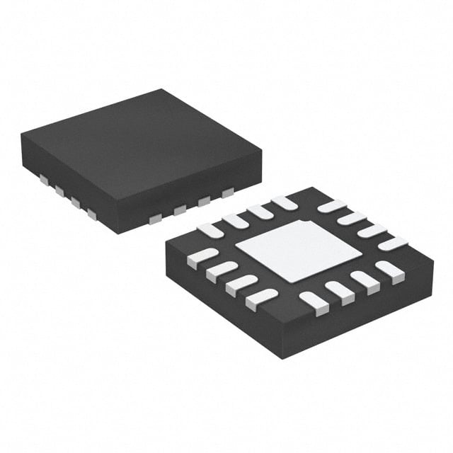
ICGOO在线商城 > 集成电路(IC) > PMIC - 配电开关,负载驱动器 > TPS2540RTET
- 型号: TPS2540RTET
- 制造商: Texas Instruments
- 库位|库存: xxxx|xxxx
- 要求:
| 数量阶梯 | 香港交货 | 国内含税 |
| +xxxx | $xxxx | ¥xxxx |
查看当月历史价格
查看今年历史价格
TPS2540RTET产品简介:
ICGOO电子元器件商城为您提供TPS2540RTET由Texas Instruments设计生产,在icgoo商城现货销售,并且可以通过原厂、代理商等渠道进行代购。 TPS2540RTET价格参考。Texas InstrumentsTPS2540RTET封装/规格:PMIC - 配电开关,负载驱动器, 。您可以下载TPS2540RTET参考资料、Datasheet数据手册功能说明书,资料中有TPS2540RTET 详细功能的应用电路图电压和使用方法及教程。
| 参数 | 数值 |
| 产品目录 | 集成电路 (IC)半导体 |
| 描述 | IC USB PWR SW/CTLR CHRG 16-WQFNUSB开关IC USB Charging Port Pwr Swtch &Contrller |
| 产品分类 | PMIC - 电源分配开关集成电路 - IC |
| 品牌 | Texas Instruments |
| 产品手册 | |
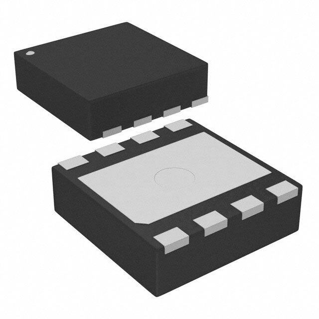
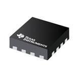
| 产品图片 |
|
| rohs | 符合RoHS无铅 / 符合限制有害物质指令(RoHS)规范要求 |
| 产品系列 | 开关 IC,USB开关IC,Texas Instruments TPS2540RTET- |
| 数据手册 | |
| 产品型号 | TPS2540RTET |
| Rds(On) | 73 毫欧 |
| 产品种类 | USB开关IC |
| 供应商器件封装 | 16-WQFN(3x3) |
| 其它名称 | 296-27900-1 |
| 内部开关 | 是 |
| 制造商产品页 | http://www.ti.com/general/docs/suppproductinfo.tsp?distId=10&orderablePartNumber=TPS2540RTET |
| 包装 | 剪切带 (CT) |
| 商标 | Texas Instruments |
| 安装类型 | 表面贴装 |
| 安装风格 | SMD/SMT |
| 封装 | Reel |
| 封装/外壳 | 16-WFQFN 裸露焊盘 |
| 封装/箱体 | WQFN-16 |
| 工作温度 | -40°C ~ 85°C |
| 工作温度范围 | - 40 C to + 85 C |
| 工厂包装数量 | 250 |
| 开关数量 | Single |
| 开关类型 | USB 开关 |
| 最大工作温度 | + 85 C |
| 最小工作温度 | - 40 C |
| 标准包装 | 1 |
| 比率-输入:输出 | 1:1 |
| 特性 | - |
| 电压-负载 | 4.5 V ~ 5.5 V |
| 电压-输入 | 4.5 V ~ 5.5 V |
| 电流-输出(最大值) | 可调 |
| 电流限制 | 2.5A |
| 电源电压-最大 | 5.5 V |
| 电源电压-最小 | 4.5 V |
| 电源电流 | 30 mA |
| 类型 | USB 开关 |
| 系列 | TPS2540 |
| 输入类型 | 非反相 |
| 输出数 | 1 |
| 输出类型 | - |





- 商务部:美国ITC正式对集成电路等产品启动337调查
- 曝三星4nm工艺存在良率问题 高通将骁龙8 Gen1或转产台积电
- 太阳诱电将投资9.5亿元在常州建新厂生产MLCC 预计2023年完工
- 英特尔发布欧洲新工厂建设计划 深化IDM 2.0 战略
- 台积电先进制程称霸业界 有大客户加持明年业绩稳了
- 达到5530亿美元!SIA预计今年全球半导体销售额将创下新高
- 英特尔拟将自动驾驶子公司Mobileye上市 估值或超500亿美元
- 三星加码芯片和SET,合并消费电子和移动部门,撤换高东真等 CEO
- 三星电子宣布重大人事变动 还合并消费电子和移动部门
- 海关总署:前11个月进口集成电路产品价值2.52万亿元 增长14.8%



PDF Datasheet 数据手册内容提取
TPS2540, TPS2540A TPS2541, TPS2541A www.ti.com SLVSAG2C–OCTOBER2010–REVISEDOCTOBER2011 USB Charging Port Power Switch and Controller CheckforSamples:TPS2540,TPS2540A,TPS2541,TPS2541A FEATURES DESCRIPTION 1 • MeetsBatteryChargingSpecificationBC1.2 The TPS2540/40A and TPS2541/41A are a 2 combination of current-limited USB port power switch forDCPandCDP with a USB 2.0 high-speed data line (D+/D-) switch • MeetsChineseTelecommunicationsIndustry and a USB charging port identification circuit. StandardYD/T1591-2009 Applications include notebook PCs and other • SupportsSleep-ModeChargingforMost intelligentUSBhostdevices.Thewidebandwidth(2.6 AvailableApple®Devicesand/orBC1.2 GHz) data-line switch also features low capacitance CompliantDevices and low on resistance, allowing signals to pass with minimum edge and phase distortion. The • CompatibleWithUSB2.0and3.0Power TPS2540/40A/41/41A monitors D+ and D-, providing SwitchRequirements the correct hand-shaking protocol with compliant • 2.6-GHzBandwidthUSB2.0DataSwitch clientdevices. • 73-mΩ (typ.)High-SideMOSFET The TPS2540/40A/41/41A supports the following • AdjustableCurrentLimitupto2.8A(typical) charginglogicschemes: • OUTDischargeThroughCTLx=000 • USB2.0BC1.2 (TPS2540/40A)orDSC(TPS2541/41A)Input • ChineseTelecomStandardYD/T1591-2009 • LongerDetachDetectionTime(TPS2540A/41A) • Divider Mode, compliant with Apple devices such SupportingAdditionalLegacyDevices asiPod®andiPhone® • Availablein16-PinQFNPackage CTL1-CTL3 logic inputs are used to select one of the various charge modes provided by the TPS2540/40A APPLICATIONS and TPS2541/41A. These charge modes allow the host device to actively select between Dedicated • USBPorts/Hubs Charging Port (DCP) (wall-adapter emulation), • NotebookPCs Charging Downstream Port (CDP) (active USB 2.0 • UniversalWallChargingAdapter data communications with 1.5-A support), or Standard Downstream Port (SDP) USB 2.0 Mode (active USB 2.0 data communications with 500-mA support). The TPS2540/40A/41/41A also integrates an auto-detect feature that supports both DCP schemes for Battery Charging Specification (BC1.2) and the Divider Mode without the need for outside userinteraction. TPS2540/40A/41/41A RTE Package and Typical Application Diagram ToSystemBus ToPeripheral TPS2540/40A/41/41A RTE Package TPS2540/40A/41/41A (Top View) 4.5Vto5.5V 1 IN OUT 12 ILIM0 ILIM1 GND FAULT R10FAkUWLT 0.1mF ILIM0 16 CUSB VDDGB-+NUDS 16 15 14 13 ILIM1 15 2x FAULTSignal 13 FAULT RILIM IN 1 12 OUT GND 14 DM_OUT 2 11 DM_IN ILIMSelect 4 ILIM_SEL Exposed DP_OUT 3 Thermal Die 10 DP_IN PowerSwitchEN 5 EN/DSC DM_IN 11 ILIM_SEL 4 9 N/C ModeSelectI/O 6 CTL1 DP_IN 10 ModeSelectI/O 7 CTL2 DM_OUT 2 5 6 7 8 ToHostController N/DSC CTL1 CTL2 CTL3 ModeSelectI/O 8 CTL3 DP_OUT 3 UDG-10116 E 1 Pleasebeawarethatanimportantnoticeconcerningavailability,standardwarranty,anduseincriticalapplicationsofTexas Instrumentssemiconductorproductsanddisclaimerstheretoappearsattheendofthisdatasheet. Apple,iPod,iPhoneareregisteredtrademarksofAppleInc. 2 PRODUCTIONDATAinformationiscurrentasofpublicationdate. Copyright©2010–2011,TexasInstrumentsIncorporated Products conform to specifications per the terms of the Texas Instruments standard warranty. Production processing does not necessarilyincludetestingofallparameters.
TPS2540, TPS2540A TPS2541, TPS2541A SLVSAG2C–OCTOBER2010–REVISEDOCTOBER2011 www.ti.com This integrated circuit can be damaged by ESD. Texas Instruments recommends that all integrated circuits be handled with appropriateprecautions.Failuretoobserveproperhandlingandinstallationprocedurescancausedamage. ESDdamagecanrangefromsubtleperformancedegradationtocompletedevicefailure.Precisionintegratedcircuitsmaybemore susceptibletodamagebecauseverysmallparametricchangescouldcausethedevicenottomeetitspublishedspecifications. DESCRIPTION (CONT.) The TPS2540A/41A auto detect mode also has a longer detach detection time, so that it can support certain unique non-compliant devices. The TPS2540/40A/41/41A power-distribution switch is intended for applications where heavy capacitive loads and short-circuits are likely to be encountered, incorporating a 73-mΩ, N-channel MOSFET in a single package. Constant-current mode is used when the output load exceeds the current-limit threshold. ILIM_SEL logic input selects one of two current-limit thresholds, each one being individually adjustable via an external resistor. Additional USB switch features include a de-glitched output fault reporting (FAULT), and a logic-level enable EN (TPS2540/40A) or OUT discharge control DSC (TPS2541/41A). With the TPS2540/40A, themode“000”isusedtoforceanoutputdischarge. PRODUCTINFORMATION(1) T FUNCTION T (2) PACKAGE MARKING A DCPLOW Enable 2540 ≤0.9s OutputDischarge 2541 -40°Cto85°C QFN16 Enable 2540A ≤9s OutputDischarge 2541A (1) Forthemostcurrentpackageandorderinginformation,seethePackageOptionAddendumattheendofthisdocument,orvisitthe deviceproductfolderonwww.ti.com. (2) LowDP_INperiodinDCPmode,seeFigure31. 2 SubmitDocumentationFeedback Copyright©2010–2011,TexasInstrumentsIncorporated ProductFolderLink(s):TPS2540,TPS2540ATPS2541,TPS2541A
TPS2540, TPS2540A TPS2541, TPS2541A www.ti.com SLVSAG2C–OCTOBER2010–REVISEDOCTOBER2011 ABSOLUTE MAXIMUM RATINGS(1) overoperatingfree-airtemperaturerange,voltagesarereferencedtoGND(unlessotherwisenoted) PARAMETER MIN MAX UNIT Supplyvoltagerange IN -0.3 7 Inputvoltagerange EN(TPS2540/40A),DSC(TPS2541/41A),ILIM0,ILIM1, -0.3 7 ILIM_SEL,CTL1,CTL2,CTL3 Voltagerange OUT,FAULT (2) -0.3 7 V Voltagerange INtoOUT -7 7 Voltagerange DP_IN,DM_IN,DP_OUT,DM_OUT (IN+0.3) -0.3 or5.7 Inputclampcurrent DP_IN,DM_IN,DP_OUT,DM_OUT ±20 ContinuouscurrentinSDPorCDP DP_INtoDP_OUTorDM_INtoDM_OUT ±100 mode mA ContinuouscurrentinBC1.2DCP DP_INtoDM_IN ±35 mode Continuousoutputcurrent I Internallylimited OUT Continuousoutputsinkcurrent FAULT 25 mA Continuousoutputsourcecurrent ILIM0,ILIM1 1 Continuoustotalpowerdissipation Internallylimited ESDrating,HumanBodyModel IN,ILIM_SEL,EN,DSC,CTL1,CTL2,CTL3,N/C,OUT, 2 (HBM) FAULT,GND,ILIM1,ILIM0 kV DP_IN,DM_IN,DP_OUT,DM_OUT 8 ESDrating,ChargedDeviceModel 500 V (CDM) OperatingJunctiontemperature T Internallylimited J Storagetemperaturerange T -65 150 °C stg (1) Stressesbeyondthoselistedunder"absolutemaximumratings"maycausepermanentdamagetothedevice.Thesearestressratings onlyandfunctionaloperationofthedeviceattheseoranyotherconditionsbeyondthoseindicatedunder"recommendedoperating conditions"isnotimplied.Exposuretoabsolute-maximum-ratedconditionsforextendedperiodsmayaffectdevicereliability. (2) Donotapplyexternalvoltagesourcesdirectly. Copyright©2010–2011,TexasInstrumentsIncorporated SubmitDocumentationFeedback 3 ProductFolderLink(s):TPS2540,TPS2540ATPS2541,TPS2541A
TPS2540, TPS2540A TPS2541, TPS2541A SLVSAG2C–OCTOBER2010–REVISEDOCTOBER2011 www.ti.com RECOMMENDED OPERATING CONDITIONS overoperatingfree-airtemperaturerange(unlessotherwisenoted) PARAMETER MIN NOM MAX UNIT V Inputvoltage,IN 4.5 5.5 IN Inputvoltage,logic-levelinputs, (CTL1,CTL2,CTL3,EN(TPS2540/40A),DSC(TPS2541/41A), 0 5.5 V ILIM_SEL) Inputvoltage,datalineinputs,(DP_IN,DM_IN,DP_OUT,DM_OUT) 5.5 Continuouscurrent,datalineinputs, ±30 (SDPorCDPmode,DP_INtoDP_OUTorDM_INtoDM_OUT) mA Continuouscurrent,datalineinputs,(BC1.2DCPmode,DP_INto ±10 DM_IN) I Continuousoutputcurrent,OUT 0 2.5 A OUT R Current-limitsetresistors,(ILIM0toGND,ILIM1toGND) 16.9 750 kΩ ILIMx T Operatingvirtualjunctiontemperature -40 125 °C J THERMAL INFORMATION TPS2540 TPS2540A TPS2541 THERMALMETRIC(1) TPS2541A UNITS RTE 16PINS θ Junction-to-ambientthermalresistance(2) 53.4 JA θ Junction-to-case(top)thermalresistance(3) 51.4 JCtop θ Junction-to-boardthermalresistance(4) 17.2 JB °C/W ψ Junction-to-topcharacterizationparameter(5) 3.7 JT ψ Junction-to-boardcharacterizationparameter(6) 20.7 JB θ Junction-to-case(bottom)thermalresistance(7) 3.9 JCbot (1) Formoreinformationabouttraditionalandnewthermalmetrics,seetheICPackageThermalMetricsapplicationreport,SPRA953. (2) Thejunction-to-ambientthermalresistanceundernaturalconvectionisobtainedinasimulationonaJEDEC-standard,high-Kboard,as specifiedinJESD51-7,inanenvironmentdescribedinJESD51-2a. (3) Thejunction-to-case(top)thermalresistanceisobtainedbysimulatingacoldplatetestonthepackagetop.Nospecific JEDEC-standardtestexists,butaclosedescriptioncanbefoundintheANSISEMIstandardG30-88. (4) Thejunction-to-boardthermalresistanceisobtainedbysimulatinginanenvironmentwitharingcoldplatefixturetocontrolthePCB temperature,asdescribedinJESD51-8. (5) Thejunction-to-topcharacterizationparameter,ψ ,estimatesthejunctiontemperatureofadeviceinarealsystemandisextracted JT fromthesimulationdataforobtainingθ ,usingaproceduredescribedinJESD51-2a(sections6and7). JA (6) Thejunction-to-boardcharacterizationparameter,ψ ,estimatesthejunctiontemperatureofadeviceinarealsystemandisextracted JB fromthesimulationdataforobtainingθ ,usingaproceduredescribedinJESD51-2a(sections6and7). JA (7) Thejunction-to-case(bottom)thermalresistanceisobtainedbysimulatingacoldplatetestontheexposed(power)pad.Nospecific JEDECstandardtestexists,butaclosedescriptioncanbefoundintheANSISEMIstandardG30-88. 4 SubmitDocumentationFeedback Copyright©2010–2011,TexasInstrumentsIncorporated ProductFolderLink(s):TPS2540,TPS2540ATPS2541,TPS2541A
TPS2540, TPS2540A TPS2541, TPS2541A www.ti.com SLVSAG2C–OCTOBER2010–REVISEDOCTOBER2011 ELECTRICAL CHARACTERISTICS Conditionsare-40≤T ≤125°Cunlessotherwisenoted.V (ifTPS2540orTPS2540A)=V (ifTPS2541orTPS2541A)= J EN DSC V =5V,R =10kΩ,R =210kΩ,R =20kΩ,I =0V,CTL1=CTL2=GND,CTL3=V (TPS2540/40A)or IN FAULT ILIM0 ILIM1 LIM_SEL IN CTL3=GND(TPS2541/41A),unlessotherwisenoted.Positivecurrentsareintopins.Typicalvaluesareat25°C.Allvoltages arewithrespecttoGNDunlessotherwisenoted. PARAMETER TESTCONDITIONS MIN TYP MAX UNIT PowerSwitch I =2A,V =LogicHI 73 120 OUT ILIM_SEL Staticdrain-source IOUT=100mA,VILIM_SEL=LogicLO 73 120 R mΩ DS(on) on-stateresistance -40°C≤T =T ≤85°C,I =2A,V =LogicHI 73 105 A J OUT ILIM_SEL T =T =25°C,I =2A,V =LogicHI 73 84 A J OUT ILIM_SEL t Risetime,output C =1µF,RL=100Ω,(seeFigure27,Figure28) 1 1.5 r L ms t Falltime,output C =1µF,RL=100Ω,(seeFigure27,Figure28) 0.2 0.5 f L OUTdischarge R 400 500 630 Ω DIS resistance I Reverseleakagecurrent V =5.5V,V =V =0V,T =25°C 0 1 µA REV OUT IN EN J EnableInputEN(TPS2540/40A),OutputDischargeInputDSC(TPS2541/41A) Enablepinturnon/off V 0.9 1.1 1.65 V EN threshold,falling V ENHysteresis 200 mV EN_HYS I Inputcurrent V =0Vor5.5V -0.5 0.5 µA EN EN DSCpinturnon/off V 0.9 1.1 1.65 V DSC threshold,falling V DSCHysteresis 200 mV DSC_HYS I Inputcurrent V =0Vor5.5V -0.5 0.5 µA DSC DSC t Turn-ontime C =1µF,R =100Ω(seeFigure27,Figure29) 3.4 5 ON L L ms t Turn-offtime C =1µF,R =100Ω(seeFigure27,Figure29) 1.7 3 OFF L L CurrentLimit I turnon/off V LIM_SEL 0.9 1.1 1.65 V ILIM_SEL threshold,falling V I Hysteresis 200 mV ILIM_HYS LIM_SEL ILIM_SELinputcurrent V =0Vor5.5V -0.5 0.5 µA ILIM_SEL R =210kΩ 185 230 265 ILIM0 V =LogicLO ILIM_SEL R =100kΩ 420 480 530 ILIM0 MaximumDCoutput RILIM1=20kΩ 2150 2430 2650 I V =LogicHI mA SHORT currentfromINtoOUT ILIM_SEL R =16.9kΩ 2550 2840 3100 ILIM1 R =698kΩ ILIM0 V =LogicLO 25 55 85 ILIM_SEL -40≤T ≤85°C J Responsetimeto t V =5.0V(seeFigure30) 1.5 µs IOS short-circuit IN SupplyCurrent Supplycurrent,switch I V =V =0V,OUTgrounded,-40≤T ≤85°C 0.1 2 CCL disabled EN DSC J V =Logic ILIM_SEL 150 185 µA HI I Supplycurrent,operating V =V =V , CCH EN DSC IN V =Logic ILIM_SEL 130 170 LOW Copyright©2010–2011,TexasInstrumentsIncorporated SubmitDocumentationFeedback 5 ProductFolderLink(s):TPS2540,TPS2540ATPS2541,TPS2541A
TPS2540, TPS2540A TPS2541, TPS2541A SLVSAG2C–OCTOBER2010–REVISEDOCTOBER2011 www.ti.com ELECTRICAL CHARACTERISTICS (continued) Conditionsare-40≤T ≤125°Cunlessotherwisenoted.V (ifTPS2540orTPS2540A)=V (ifTPS2541orTPS2541A)= J EN DSC V =5V,R =10kΩ,R =210kΩ,R =20kΩ,I =0V,CTL1=CTL2=GND,CTL3=V (TPS2540/40A)or IN FAULT ILIM0 ILIM1 LIM_SEL IN CTL3=GND(TPS2541/41A),unlessotherwisenoted.Positivecurrentsareintopins.Typicalvaluesareat25°C.Allvoltages arewithrespecttoGNDunlessotherwisenoted. PARAMETER TESTCONDITIONS MIN TYP MAX UNIT UndervoltageLockout Low-levelinputvoltage, V V rising 3.9 4.1 4.3 V UVLO IN IN Hysteresis,IN 100 mV FAULT Outputlowvoltage, I =1mA 100 mV FAULT FAULT Off-stateleakage V =5.5V 1 µA FAULT FAULTdeglitch FAULTassertionorde-assertionduetoover-currentcondition 5 8.5 12 ms CTLxInputs CTLxpinsturnon/off V 0.9 1.1 1.65 V CTL threshold,falling V CTLxhysteresis 200 mV CTL_HYS Inputcurrent V =0Vor5.5V -0.5 0.5 µA CTL ThermalShutdown Thermalshutdown 155 threshold Thermalshutdown °C 135 thresholdincurrent-limit Hysteresis 10 High-BandwidthAnalogSwitch OnresistanceDP/DM VDP/DM_OUT=0V,IDP/DM_IN=+30mA 2 4 R HS_ON high-speedswitch V =2.4V,I =-15mA 3 6 DP/DM_OUT DP/DM_IN Ω Onresistancematch V =0V,I =+30mA 0.05 0.15 DP/DM_OUT DP/DM_IN ΔR betweenchannels HS_ON DP/DMswitch VDP/DM_OUT=2.4V,IDP/DM_IN=-15mA 0.05 0.15 DP/DMoffstate CIO_OFF capacitance (1) f=1MHz,switchoff 3 3.6 pF DP/DMonstate CIO_ON capacitance (2) f=1MHz,switchon 5.4 6.2 O Offstateisolation R =50Ω,f=250MHz,-40≤T ≤125°C 33 IRR L J On-statecrosschannel dB X R =50Ω,f=250MHz,-40≤T ≤125°C 52 TALK isolation L J I Offstateleakage V =V =3.6V,V =V =0V 0.1 1.5 µA OFF DM_IN DP_IN DM_OUT DP_OUT BW Bandwidth(-3dB) R =50Ω 2.6 GHz L t Propagationdelay 0.25 pd Skewbetweenopposite ns t transitionsofthesame 0.1 0.2 SK port(t –t ) PHL PLH (1) TheresistanceinserieswiththisparasiticcapacitancetoGNDistypically250Ω. (2) TheresistanceinserieswiththisparasiticcapacitancetoGNDistypically150Ω. 6 SubmitDocumentationFeedback Copyright©2010–2011,TexasInstrumentsIncorporated ProductFolderLink(s):TPS2540,TPS2540ATPS2541,TPS2541A
TPS2540, TPS2540A TPS2541, TPS2541A www.ti.com SLVSAG2C–OCTOBER2010–REVISEDOCTOBER2011 ELECTRICAL CHARACTERISTICS (continued) Conditionsare-40≤T ≤125°Cunlessotherwisenoted.V (ifTPS2540orTPS2540A)=V (ifTPS2541orTPS2541A)= J EN DSC V =5V,R =10kΩ,R =210kΩ,R =20kΩ,I =0V,CTL1=CTL2=GND,CTL3=V (TPS2540/40A)or IN FAULT ILIM0 ILIM1 LIM_SEL IN CTL3=GND(TPS2541/41A),unlessotherwisenoted.Positivecurrentsareintopins.Typicalvaluesareat25°C.Allvoltages arewithrespecttoGNDunlessotherwisenoted. PARAMETER TESTCONDITIONS MIN TYP MAX UNIT DCPShortedModeChargerInterface DP_IN/DM_INshorting R CTLxconfiguredforDCPBC1.2 125 200 Ω DPM_short resistance Dischargeresistance R DM_INandDP_INto CTLxconfiguredforDCPBC1.2 2 3.2 6 MΩ DCHG_PW GND DividerModeChargerInterface V DP_INoutputvoltage 1.9 2 2.1 DP_AM V V DM_INoutputvoltage 2.57 2.7 2.84 DM_AM CTLxconfiguredfordividermode Z DP_INoutputimpedance 8 10 12.5 OUT_DP kΩ Z DM_INoutputimpedance 8 10 12.5 OUT_DM CDPInterface Voltagesourceon V V =0.6V,CTLxconfiguredforCDP 0.5 0.6 0.7 DM_SRC DM_INforCDPdetect DP_IN DP_INrisingvoltage V V thresholdtoactivate 0.25 0.4 DAT_REF V DM_SRC V hysteresis 50 mV DAT_REF I =-250µA,CTLxconfiguredforCDP DM_IN DP_INrisingvoltage V thresholdtodeactivate 0.8 1 V LGC_SRC V DM_SRC V hysteresis 100 mV LGC_SRC I DP_INsinkcurrent 0.4V≤V ≤0.8V,CTLxconfiguredforCDPoperation 50 150 µA DP_SINK DP_IN Timings DM_INvoltagesource FromV =0->0.6VtoV =V ,CTLx t DP_IN DM_IN DM_SRC 1 10 VDMSRC_EN enabletime,CDPmode configuredforCDP DM_INvoltagesource FromV =0.6V->0VtoV =0V,CTLxconfigured t DP_IN DM_IN 10 VDMSRC_DIS disabletime,CDPmode forCDP ms TimeforOUTtobe reappliedafterV falls AnytransitiontoandfromCDP,ortoandfromSDP.Also t OUT 200 500 VBUS_REAPP below0.7Vduring duringAuto-detecttoshortedmode. discharge TimingRequirements Sessionvalid(INhigh)to t TPS2540/TPS2541 1 SLVD_CON_P VDP_SRCinDCPmode s LowDP_INperiodin WhenVBUSishigh,(TPS2540,TPS2541) 0.9 t DCPLOW DCPmode WhenVBUSishigh,(TPS2540A,TPS2541A) 9 Copyright©2010–2011,TexasInstrumentsIncorporated SubmitDocumentationFeedback 7 ProductFolderLink(s):TPS2540,TPS2540ATPS2541,TPS2541A
TPS2540, TPS2540A TPS2541, TPS2541A SLVSAG2C–OCTOBER2010–REVISEDOCTOBER2011 www.ti.com DEVICE INFORMATION TPS2540,TPS2540A,TPS2541andTPS2541A TPS2540/TPS2540A TPS2541/TPS2541A RTE Package RTE Package (Top View) (Top View) T T M0 M1 D UL M0 M1 D UL ILI ILI GN FA ILI ILI GN FA 16 15 14 13 16 15 14 13 IN 1 12 OUT IN 1 12 OUT DM_OUT 2 11 DM_IN DM_OUT 2 11 DM_IN Exposed Exposed Thermal Die Thermal Die DP_OUT 3 10 DP_IN DP_OUT 3 10 DP_IN ILIM_SEL 4 9 N/C ILIM_SEL 4 9 N/C 5 6 7 8 5 6 7 8 N 1 2 3 C 1 2 3 E CTL CTL CTL DS CTL CTL CTL DetectionBlockDiagram ToHost DM_OUT 2 VBUS Controller USB CDP/SDP Conector 2.7V 10kW DM_IN VBUS 11 D- D+ DividerMode DCP CDP Auto GND 125WShorted Detect/ Detect Mode CTL 2V DP_IN 10kW 10 8 CTL3 ToHost DP_OUT CDP/SDP 3 Controller 7 CTL2 6 UDG-10126 CTL1 8 SubmitDocumentationFeedback Copyright©2010–2011,TexasInstrumentsIncorporated ProductFolderLink(s):TPS2540,TPS2540ATPS2541,TPS2541A
TPS2540, TPS2540A TPS2541, TPS2541A www.ti.com SLVSAG2C–OCTOBER2010–REVISEDOCTOBER2011 TPS2540/40A/41/41ATop-LevelFunctionalBlockDiagram IN 1 EN/DSC 5 12 OUT PowerSwitch ILIM0 16 ControlCircuitry ILIM1 15 13 FAULT ILIM_SEL 4 CTL1 6 Charge CTL2 7 Logic Auto CTL3 8 Discharge DM_OUT 2 DP_OUT 3 High 11 DM_IN Bandwidth Charging Host Downstream Switch Sense PortModeBC 10 DP_IN Divider Mode Shorted Dedicated 14 GND Mode Sense UDG-10125 Copyright©2010–2011,TexasInstrumentsIncorporated SubmitDocumentationFeedback 9 ProductFolderLink(s):TPS2540,TPS2540ATPS2541,TPS2541A
TPS2540, TPS2540A TPS2541, TPS2541A SLVSAG2C–OCTOBER2010–REVISEDOCTOBER2011 www.ti.com PIN DESCRIPTIONS PinDescriptions NAME PIN I/O DESCRIPTION PowerSwitch Inputvoltage;connecta0.1-µForgreaterceramiccapacitorfromINtoGNDasclose IN 1 PWR tothedeviceaspossible. OUT 12 PWR Power-switchoutput. GND 14 PWR Groundconnection;shouldbeconnectedexternallytoPowerPAD. InternallyconnectedtoGND;usedtoheat-sinktheparttothecircuitboardtraces. POWERPAD N/A ConnecttoGNDplane. Current-LimitThreholdsandIndication Externalresistorusedtosetcurrent-limitthresholdwhenILIM_SELisLO; ILIM0 16 I recommended16.9kΩ≤R ≤750kΩ; ILIM Externalresistorusedtosetcurrent-limitthresholdwhenILIM_SELisHI; ILIM1 15 I recommended16.9kΩ≤R ≤750kΩ; ILIM Logic-levelinputsignalusedtodynamicallychangepowerswitchcurrent-limit ILIM_SEL 4 I threshold;logicLOselectsILIM0,logicHIselectsILIM1. Active-lowopen-drainoutput,assertedduringover-temperatureorcurrentlimit FAULT 13 O conditions. InputLogicControlSignals Logic-levelcontrolinputforturningthepowerswitchandthesignalswitcheson/off. TPS2540/40A:WhenENislow,thedeviceisdisabled,thesignalandpower EN,DSC 5 I switchesareOFF. TPS2541/41A:WhenDSCislow,thedeviceisdisabled,thesignalandpower switchesareOFFandtheoutput(OUT)capacitorisdischarged. CTL1 6 I Logic-levelcontrolinputsforcontrollingthechargingmodeandthesignalswitches. TheTPS2540/40AandTPS2541/41Ausedifferentcontrollinetruthtables.Withthe CTL2 7 I TPS2540/40A,the“000”configurationisusedtoforceadischargeoftheoutput CTL3 8 I (OUT)capacitor. D+/D-DataLineSignals D-datalinetoconnector,input/outputusedforhand-shakingwithportable DM_IN 11 I/O equipment. D+datalinetoconnector,input/outputusedforhand-shakingwithportable DP_IN 10 I/O equipment. DM_OUT 2 I/O D-datalinetoUSBhostcontroller. DP_OUT 3 I/O D+datalinetoUSBhostcontroller. N/C 9 Noconnectpin.Canbegroundedorleftfloating. 10 SubmitDocumentationFeedback Copyright©2010–2011,TexasInstrumentsIncorporated ProductFolderLink(s):TPS2540,TPS2540ATPS2541,TPS2541A
TPS2540, TPS2540A TPS2541, TPS2541A www.ti.com SLVSAG2C–OCTOBER2010–REVISEDOCTOBER2011 TYPICAL CHARACTERISTICS INUVLORISING SUPPLYCURRENT-DISABLED vs vs TEMPERATURE TEMPERATURE 4.5 1 4.4 0.9 0.8 4.3 0.7 V 4.2 A m VLO- 4.1 ent- 0.6 U urr 0.5 N C -I 4 N O I 0.4 VUVL 3.9 -CCL I 0.3 3.8 0.2 3.7 0.1 3.6 0 -40 -20 0 20 40 60 80 100 120 140 -40 -20 0 20 40 60 80 100 120 140 T -JunctionTemperature-°C T -JunctionTemperature-°C J J Figure1. Figure2. SUPPLYCURRENT-SDPorDCPBC SUPPLYCURRENT-AUTO-DETECT vs vs TEMPERATURE TEMPERATURE 120 150 110 140 A 100 A m m nt- nt- 130 e e r r ur 90 ur C C N N I I 120 - - H H C 80 C C C I I 110 70 60 100 -40 -20 0 20 40 60 80 100 120 140 -40 -20 0 20 40 60 80 100 120 140 T -JunctionTemperature-°C T -JunctionTemperature-°C J J Figure3. Figure4. Copyright©2010–2011,TexasInstrumentsIncorporated SubmitDocumentationFeedback 11 ProductFolderLink(s):TPS2540,TPS2540ATPS2541,TPS2541A
TPS2540, TPS2540A TPS2541, TPS2541A SLVSAG2C–OCTOBER2010–REVISEDOCTOBER2011 www.ti.com TYPICAL CHARACTERISTICS (continued) SUPPLYCURRENT-CDPorDIVIDERMODE CURRENTLIMIT vs vs TEMPERATURE CURRENTLIMITRESISTANCE 150 3000 T =25°C J 2500 140 A m A m - 2000 ent- 130 Limit Curr rent 1500 N ur I 120 C - H - ICC HORT 1000 S I 110 500 100 0 -40 -20 0 20 40 60 80 100 120 140 0 20 40 60 80 100 120 140 160180 200220 240 T -JunctionTemperature-°C R -CurrentLimitResistance-kW J ILIM Figure5. Figure6. CURRENTLIMIT POWERSWITCHON-RESISTANCE vs vs TEMPERATURE TEMPERATURE 2500 100 95 W 2000 R =20kW m 90 ILIM - A e m c 85 n - a Limit 1500 esist 80 R rent ON 75 ur R =100kW T C 1000 ILIM R =210kW U 70 - ILIM O RT N/ O I 65 ISH -n) o 500 DS( 60 R 55 0 50 -40 -20 0 20 40 60 80 100 120 140 -40 -20 0 20 40 60 80 100 120 140 T -JunctionTemperature-°C T -JunctionTemperature-°C J J Figure7. Figure8. 12 SubmitDocumentationFeedback Copyright©2010–2011,TexasInstrumentsIncorporated ProductFolderLink(s):TPS2540,TPS2540ATPS2541,TPS2541A
TPS2540, TPS2540A TPS2541, TPS2541A www.ti.com SLVSAG2C–OCTOBER2010–REVISEDOCTOBER2011 TYPICAL CHARACTERISTICS (continued) TURN-ONTIME,TURN-OFFTIME DATASWITCHON-RESISTANCE vs vs TEMPERATURE TEMPERATURE 5 5 4.5 W ms 4 Turn-OnTime ce- 4 VDP/DM_OUT=2.4V,IDP/DM_IN=-15mA - n me sta 3.5 Ti esi F 3 R 3 F O N ON/ hO 2.5 Turn- 2 Switc 2 T-OFF Turn-OffTime -Data 1.5 VDP/DM_OUT=0V,IDP/DM_IN=30mA /ON 1 on) 1 T S( H R 0.5 0 0 -40 -20 0 20 40 60 80 100 120 140 -40 -20 0 20 40 60 80 100 120 140 T -JunctionTemperature-°C T -JunctionTemperature-°C J J Figure9. Figure10. FAULTOUTPUTVOLTAGE ENTHRESHOLDFALLING vs vs SINKCURRENT TEMPERATURE 700 2 1.8 600 TJ=125°C 1.6 V mV 500 d- 1.4 ol - h ge es 1.2 olta 400 TJ=25°C Thr V g 1 w n Lo 300 Falli 0.8 T L N U E A 200 - 0.6 F N E V 0.4 100 TJ=-40°C 0.2 0 0 0 1 2 3 4 5 6 7 8 9 10 -40 -20 0 20 40 60 80 100 120 140 I -FAULTSinkCurrent-mA T -JunctionTemperature-°C FAULT J Figure11. Figure12. Copyright©2010–2011,TexasInstrumentsIncorporated SubmitDocumentationFeedback 13 ProductFolderLink(s):TPS2540,TPS2540ATPS2541,TPS2541A
TPS2540, TPS2540A TPS2541, TPS2541A SLVSAG2C–OCTOBER2010–REVISEDOCTOBER2011 www.ti.com TYPICAL CHARACTERISTICS (continued) CTL1-3THRESHOLDFALLING DIVIDERMODEDP/DMVOLTAGE vs vs TEMPERATURE TEMPERATURE 2 3 1.8 2.8 DM_INVoltage V 1.6 - 2.6 e V ag d- 1.4 olt 2.4 ol V Thresh 1.2 Output 2.2 g 1 e 2 n pl alli 0.8 Ap 1.8 DP_INVoltage F N 1-3 0.6 M_I 1.6 L T D C N/ 0.4 _I 1.4 P D 0.2 1.2 0 1 -40 -20 0 20 40 60 80 100 120 140 -40 -20 0 20 40 60 80 100 120 140 T -JunctionTemperature-°C T -JunctionTemperature-°C J J Figure13. Figure14. DATATRANSMISSIONCHARACTERISTICS OFFSTATEDATASWITCHISOLATION vs vs FREQUENCY FREQUENCY 0 60 50 -5 B d B d n- 40 - o Gain -10 olati s on eI 30 si at mis -15 St ns Off 20 Tra -RR OI -20 10 -20 0 0.01 0.1 1 10 0.01 0.1 1 10 Frequency-GHz Frequency-GHz Figure15. Figure16. 14 SubmitDocumentationFeedback Copyright©2010–2011,TexasInstrumentsIncorporated ProductFolderLink(s):TPS2540,TPS2540ATPS2541,TPS2541A
TPS2540, TPS2540A TPS2541, TPS2541A www.ti.com SLVSAG2C–OCTOBER2010–REVISEDOCTOBER2011 TYPICAL CHARACTERISTICS (continued) ONSTATECROSS-CHANNELISOLATION vs FREQUENCY 80 B d - 70 n o ati 60 ol s I el n 50 n a h C 40 s- s o r C 30 e at St N 20 O - K AL 10 T X 0 0.01 0.1 1 10 Frequency-GHz Figure17. EYEDIAGRAMUSINGUSBCOMPLIANCETESTPATTERN EYEDIAGRAMUSINGUSBCOMPLIANCETESTPATTERN (withnoswitch) (withdataswitch) 0.5 0.5 0.4 0.4 0.3 0.3 V 0.2 V 0.2 - - al al n 0.1 n 0.1 g g Si Si 0 0 al al enti -0.1 enti -0.1 r r e e Diff -0.2 Diff -0.2 -0.3 -0.3 -0.4 -0.4 -0.5 -0.5 0 0.2 0.4 0.6 0.8 1 1.2 1.4 1.6 1.8 2 0 0.2 0.4 0.6 0.8 1 1.2 1.4 1.6 1.8 2 t-Time(x10-9)-s t-Time(x10-9)-s Figure18. Figure19. Copyright©2010–2011,TexasInstrumentsIncorporated SubmitDocumentationFeedback 15 ProductFolderLink(s):TPS2540,TPS2540ATPS2541,TPS2541A
TPS2540, TPS2540A TPS2541, TPS2541A SLVSAG2C–OCTOBER2010–REVISEDOCTOBER2011 www.ti.com TYPICAL CHARACTERISTICS (continued) EYEDIAGRAMOFNEARLYIDEALPULSE EYEDIAGRAMOFNEARLYIDEALPULSE (withnoswitch) (withdataswitch) v. v. di di V/ V/ m m 0 0 0 0 2 2 348ps/div. 348ps/div. Figure20. Figure21. TURNONINTOASHORTCIRCUIT TURNONINTOASHORTCIRCUIT IN(2V/div.) IN(2V/div.) OUT(2V/div.) I_IN(0.5A/div.) I_IN(0.5A/div.) OUT(2V/div.) 0.2s/div 10ms/div Figure22. Figure23. 16 SubmitDocumentationFeedback Copyright©2010–2011,TexasInstrumentsIncorporated ProductFolderLink(s):TPS2540,TPS2540ATPS2541,TPS2541A
TPS2540, TPS2540A TPS2541, TPS2541A www.ti.com SLVSAG2C–OCTOBER2010–REVISEDOCTOBER2011 TYPICAL CHARACTERISTICS (continued) RESPONSETOASHORT-CIRCUIT RESPONSETOASHORT-CIRCUIT (fromno-loadcondition) (fromno-loadcondition) IN(2V/div.) OUT(2V/div.) IN(2V/div.) OUT(2V/div.) I_IN(2A/div.) I_IN(2A/div.) 100ms/div 1ms/div Figure24. Figure25. RESPONSETOASHORT-CIRCUITFROMNOLOADCONDITION (withTPS51117EVMsource) IN(1V/div.) OUT(1V/div.) I_IN(2A/div.) 2ms/div Figure26. Copyright©2010–2011,TexasInstrumentsIncorporated SubmitDocumentationFeedback 17 ProductFolderLink(s):TPS2540,TPS2540ATPS2541,TPS2541A
TPS2540, TPS2540A TPS2541, TPS2541A SLVSAG2C–OCTOBER2010–REVISEDOCTOBER2011 www.ti.com PARAMETER MEASUREMENT INFORMATION OUT R C L L Figure27. TestCircuit t t r f 90% 90% V 10% 10% OUT UDG-10140 Figure28. VoltageWaveform 50% 50% t OFF V EN t ON 90% V 10% OUT UDG-10117 Figure29. VoltageWaveforms I OS I OUT UDG-10118 t IOS Figure30. ResponseTimetoShort-CircuitWaveform 18 SubmitDocumentationFeedback Copyright©2010–2011,TexasInstrumentsIncorporated ProductFolderLink(s):TPS2540,TPS2540ATPS2541,TPS2541A
TPS2540, TPS2540A TPS2541, TPS2541A www.ti.com SLVSAG2C–OCTOBER2010–REVISEDOCTOBER2011 t SVLD_CON_P OUT V DP_IN LGC_SRC V DAT_REF 0V V LGC_SRC DM_IN V DAT_REF 0V t t UDG-10119 DCPLOW DCPLOW Figure31. DCPBC1.2Operation CTL1-3 SDPorCDP OUT 0.7V UDG-10120 t VBUS_REAPP Figure32. OUTDischargeDuringCTLxLinesChange Copyright©2010–2011,TexasInstrumentsIncorporated SubmitDocumentationFeedback 19 ProductFolderLink(s):TPS2540,TPS2540ATPS2541,TPS2541A
TPS2540, TPS2540A TPS2541, TPS2541A SLVSAG2C–OCTOBER2010–REVISEDOCTOBER2011 www.ti.com DividerOnlyMode 5V 1 NetworkAnalyzer IN 50W DP_IN DP_OUT 10 3 SourceSignal 50W DM_IN DM_OUT 50W 11 2 50W GND 50W 14 UDG-10141 Figure33. OFFStateIsolation(O ) IRR 5V 1 IN DP_IN DP_OUT 10 3 50W 50W NetworkAnalyzer 50W DM_IN DM_OUT 11 2 SourceSignal 50W GND 14 50W UDG-10121 Figure34. OFFStateIsolation(O ) IRR NetworkAnalyzerSetup • Sourcesignal=600-mVpeak-to-peakat50-Ωload • DCbias=300mV 20 SubmitDocumentationFeedback Copyright©2010–2011,TexasInstrumentsIncorporated ProductFolderLink(s):TPS2540,TPS2540ATPS2541,TPS2541A
TPS2540, TPS2540A TPS2541, TPS2541A www.ti.com SLVSAG2C–OCTOBER2010–REVISEDOCTOBER2011 SDPMode 5V 1 IN DP_IN DP_OUT 10 3 50W NetworkAnalyzer 50W DM_IN DM_OUT 11 2 SourceSignal GND 50W 14 50W UDG-10142 Figure35. ONStateCrossChannelIsolation(X ) TALK 5V 1 NetworkAnalyzer IN 50W DP_IN DP_OUT 10 3 SourceSignal 50W DM_IN DM_OUT 50W 11 2 50W GND 14 UDG-10122 Figure36. ONStateCrossChannelIsolation(X ) TALK NetworkAnalyzerSetup • Sourcesignal=600-mVpeak-to-peakat50-Ωload • DCbias=300mV Copyright©2010–2011,TexasInstrumentsIncorporated SubmitDocumentationFeedback 21 ProductFolderLink(s):TPS2540,TPS2540ATPS2541,TPS2541A
TPS2540, TPS2540A TPS2541, TPS2541A SLVSAG2C–OCTOBER2010–REVISEDOCTOBER2011 www.ti.com SDPMode 5V 1 NetworkAnalyzer IN 50W DP_IN DP_OUT 10 3 SourceSignal DM_IN DM_OUT 50W 11 2 GND 50W 14 UDG-10143 Figure37. Bandwidth(BW) 5V 1 IN DP_IN DP_OUT 10 3 50W NetworkAnalyzer 50W DM_IN DM_OUT 11 2 SourceSignal GND 14 50W UDG-10123 Figure38. Bandwidth(BW) NetworkAnalyzerSetup • Sourcesignal=600-mVpeak-to-peakat50-Ωload • DCbias=300mV 22 SubmitDocumentationFeedback Copyright©2010–2011,TexasInstrumentsIncorporated ProductFolderLink(s):TPS2540,TPS2540ATPS2541,TPS2541A
TPS2540, TPS2540A TPS2541, TPS2541A www.ti.com SLVSAG2C–OCTOBER2010–REVISEDOCTOBER2011 SDPMode 5V 1 IN DP_IN DP_OUT 10 3 DM_IN DM_OUT + 11 2 I GND OUT 14 UDG-10124 Figure39. OnResistanceDP/DMHigh-SpeedSwitch(R ) HS_ON V -V R = DP_IN DP_OUT HS_ON I OUT (1) V -V R = DM_IN DM_OUT HS_ON I OUT (2) Copyright©2010–2011,TexasInstrumentsIncorporated SubmitDocumentationFeedback 23 ProductFolderLink(s):TPS2540,TPS2540ATPS2541,TPS2541A
TPS2540, TPS2540A TPS2541, TPS2541A SLVSAG2C–OCTOBER2010–REVISEDOCTOBER2011 www.ti.com GENERAL INFORMATION Overview The following overview references various industry standards. It is always recommended to consult the most up-to-datestandardtoensurethemostrecentandaccurateinformation. Rechargeable portable equipment requires an external power source to charge its batteries. USB ports are a convenient location for charging because of an available 5-V power source. Universally accepted standards are required to make sure host and client-side devices operate together in a system to ensure power management requirements are met. Traditionally, USB host ports following the USB 2.0 specification must provide at least 500 mA to downstream client-side devices. Because multiple USB devices can be attached to a single USB port through a bus-powered hub, it is the responsibility of the client-side device to negotiate its power allotment from the host to ensure the total current draw does not exceed 500 mA. In general, each USB device is granted 100 mA and may request more current in 100 mA unit steps up to 500 mA. The host may grant or deny based on the availablecurrent. Additionally, the success of USB has made the mini-USB connector a popular choice for wall adapter cables. ThisallowsaportabledevicetochargefrombothawalladapterandUSBportwithonlyoneconnector. One common difficulty has resulted from this. As USB charging has gained popularity, the 500 mA minimum defined by USB 2.0 has become insufficient for many handset and personal media players which need a higher charging rate. On the other hand, wall adapters can provide much more current than 500 mA. Several new standards have been introduced defining protocol handshaking methods that allow host and client devices to acknowledge and draw additional current beyond the 500 mA minimum defined by USB 2.0 while still using a singlemicro-USBinputconnector. TheTPS2540,TPS2540A,TPS2541andTPS2541Asupportthreeofthemostcommonprotocols: • USB2.0BatteryChargingSpecificationBC1.2 • ChineseTelecommunicationsIndustryStandardYD/T1591-2009 • DividerMode All three methods have similarities and differences, but the biggest commonality is that all three define three typesofchargingportsthatprovidechargingcurrenttoclient-sidedevices.Thesechargingportsaredefinedas: • StandardDownstreamPort(USB2.0)(SDP) • ChargingDownstreamPort(CDP) • DedicatedChargingPort(DCP) BC1.2 defines a Charging Port as a downstream facing USB port that provides power for charging portable equipment. ThetablebelowshowsthedifferencesbetweentheseportsaccordingtoBC1.2. Table1.OperatingModes MAXIMUMALLOWABLECURRENTDRAW PORTTYPE SUPPORTSUSB2.0COMMUNICATION BYPORTABLEEQUIPMENT(A) SDP(USB2.0) Yes 0.5 CDP Yes 1.5 DCP No 1.5 BC1.2 defines the protocol necessary to allow portable equipment to determine what type of port it is connected to so that it can allot its maximum allowable current draw. The hand-shaking process has two steps. During step one, the primary detection, the portable equipment outputs a nominal 0.6-V output on its D+ line and reads the voltage input on its D- line. The portable device concludes it is connected to an SDP if the voltage is less than the nominal data detect voltage of 0.3 V. The portable device concludes that it is connected to a Charging Port if the D- voltage is greater than the nominal data detect voltage of 0.3 V and less than 0.8 V. The second step, the secondary detection, is necessary for portable equipment to determine between a CDP and a DCP. The portable device outputs a nominal 0.6 V output on its D- line and reads the voltage input on its D+ line. The portable device concludes it is connected to a CDP if the data line being read remains less than the nominal data detect voltage of 0.3 V. The portable device concludes it is connected to a DCP if the data line being read is greater thanthenominaldatadetectvoltageof0.3Vandlessthan0.8V. 24 SubmitDocumentationFeedback Copyright©2010–2011,TexasInstrumentsIncorporated ProductFolderLink(s):TPS2540,TPS2540ATPS2541,TPS2541A
TPS2540, TPS2540A TPS2541, TPS2541A www.ti.com SLVSAG2C–OCTOBER2010–REVISEDOCTOBER2011 Standard Downstream Port (SDP) USB 2.0 An SDP is a traditional USB port that follows USB 2.0 and supplies a minimum of 500 mA per port. USB 2.0 communicationsissupported,andthehostcontrollermustbeactivetoallowcharging. Charging Downstream Port (CDP) A CDP is a USB port that follows USB 2.0 BC1.2 and supplies a minimum of 1.5 A per port. It provides power and meets USB 2.0 requirements for device enumeration. USB 2.0 communications is supported, and the host controller must be active to allow charging. What separates a CDP from an SDP is the host-charge handshaking logic that identifies this port as a CDP. A CDP is identifiable by a compliant BC1.2 client device and allows for additionalcurrentdrawbytheclientdevice. The CDP hand-shaking process is two steps. During step one the portable equipment outputs a nominal 0.6 V output on its D+ line and reads the voltage input on its D- line. The portable device concludes it is connected to an SDP if the voltage is less than the nominal data detect voltage of 0.3 V. The portable device concludes that it is connected to a Charging Port if the D- voltage is greater than the nominal data detect voltage of 0.3V and less than0.8V. The second step is necessary for portable equipment to determine between a CDP and a DCP. The portable device outputs a nominal 0.6 V output on its D- line and reads the voltage input on its D+ line. The portable device concludes it is connected to a CDP if the data line being read remains less than the nominal data detect voltage of 0.3 V. The portable device concludes it is connected to a DCP if the data line being read is greater thanthenominaldatadetectvoltageof0.3Vandlessthan0.8V. Dedicated Charging Port (DCP) A DCP is a special type of wall-adapter used in charging applications that uses a micro-B connector to connect to portable devices. A DCP only provides power and cannot enumerate upstream facing portable equipment. It does not support USB 2.0 communications, but it does provide specific impedances on the data lines reserved forUSB2.0sothatitisidentifiableasadedicatedcharger. The impedances presented on D+ and D- are different depending on the specific standard the dedicated charger is designed to. BC1.2 and the Chinese Telecommunications Industry Standard YD/T 1591-2009 define that the D+andD-datalinesshouldbeshortedtogetherwithamaximumseriesimpedanceof200Ω. Ontheotherhand,withthedividermode,2Vand2.7VarepresentedonD+andonD-. The TPS2540/40A/41/41A integrates an auto-detect feature that supports both DCP schemes. It starts in Divider Mode. If a BC1.2 -compliant device is attached, the TPS2540/40A/41/41A responds by discharging OUT, turning back ON the power switch and operating in BC1.2 DCP mode. It then stays in that mode until the device is unattached,inwhichcaseitgoesbacktoDividerMode. High-Bandwidth Data Line Switch The TPS2540/40A/41/41A passes the D+ and D- data lines through the device to enable monitoring and handshaking while supporting charging operation. A wide bandwidth signal switch is used, allowing data to pass through the device without corrupting signal integrity. The data line switches are turned on in any of CDP or SDP operating modes. The EN (or DSC if TPS2541/41A) input also needs to be at logic High for the data line switchestobeenabled. NOTE 1. WhileinCDPmode,thedataswitchesareONevenwhileCDPhandshakingisoccurring. 2. The datalineswitches are OFFifEN(or DSC) is low,orifinDCP mode (BC1.2,Divider mode or Auto-detect). They are not automatically turned off if the power switch (IN to OUT) is doing currentlimiting.WithTPS2540/40A,thedatalineswitchesarealsooffwhenin“000”mode. 3. The data switches are for USB 2.0 differential pair only. In the case of a USB 3.0 host, the super speed differential pairs must be routed directly to the USB connector without passing throughtheTPS2540/40A/41/41A. Copyright©2010–2011,TexasInstrumentsIncorporated SubmitDocumentationFeedback 25 ProductFolderLink(s):TPS2540,TPS2540ATPS2541,TPS2541A
TPS2540, TPS2540A TPS2541, TPS2541A SLVSAG2C–OCTOBER2010–REVISEDOCTOBER2011 www.ti.com Logic Control Modes BoththeTPS2540/40AandTPS2541/41AsupportthelistedstandardsabovefortheSDP,CDPandDCPmodes using the CTL1, CTL2, and CTL3 logic I/O control pins, although their truth tables are different as shown below. The different CTLx settings correspond to the different types of charge modes. Also, using the Auto-Detect Mode, the Divider Mode or BC1.2 / YD/T 1591-2009 can be automatically selected without external user interaction. NOTE With the TPS2540/40A, if the “000” mode is selected, the power switch will be turned off and an output discharge resistor will be connected, while the data line switches will be turnedoff. Table2.TPS2540/40AControlTruthTable CTL1 CTL2 CTL3 MODE 0 0 0 OUTdischarge,powerswitchOFF. 0 X 1 Dedicatedchargingport,auto-detect. X 1 0 Standarddownstreamport,USB2.0Mode. 1 0 0 Dedicatedchargingport,BC1.2only. 1 0 1 Dedicatedchargingport,DividerModeonly. 1 1 1 Chargingdownstreamport,BC1.2. Table3.TPS2541/41AControlTruthTable CTL1 CTL2 CTL3 MODE 0 0 X Dedicatedchargingport,auto-detect. 0 1 X Dedicatedchargingport,BC1.2. 1 0 X Dedicatedchargingport,DividerModeonly. 1 1 0 Standarddownstreamport,USB2.0Mode. 1 1 1 Chargingdownstreamport,BC1.2. Output Discharge To allow a charging port to renegotiate current with a portable device, TPS2540/40A/41/41A uses the VBUS discharge function. It proceeds by turning off the power switch while discharging OUT, then turning back ON the powerswitchtoreasserttheOUTvoltage. This discharge function is automatically applied when a change at the CTLx lines results in any of the following modetransitions. • AnytransitiontoandfromCDP • AnytransitiontoandfromSDP In addition to this, a direct discharge control, DSC, is available with the TPS2541/41A, while with the TPS2540/40A,adischargecanbeachievedusingthemode“000”. Overcurrent Protection When an over-current condition is detected, the device maintains a constant output current and reduces the output voltage accordingly. Two possible overload conditions can occur. In the first condition, the output has beenshortedbeforethedeviceisenabledorbeforeV hasbeenapplied. IN The TPS2540/40A/41/41A senses the short and immediately switches into a constant-current output. In the second condition, a short or an overload occurs while the device is enabled. At the instant the overload occurs, high currents may flow for nominally one to two microseconds before the current-limit circuit can react. The device operates in constant-current mode after the current-limit circuit has responded. Complete shutdown occurs only if the fault is present long enough to activate thermal limiting. The device will remain off until the junction temperature cools approximately 10°C and will then re-start. The device will continue to cycle on/off until theover-currentconditionisremoved. 26 SubmitDocumentationFeedback Copyright©2010–2011,TexasInstrumentsIncorporated ProductFolderLink(s):TPS2540,TPS2540ATPS2541,TPS2541A
TPS2540, TPS2540A TPS2541, TPS2541A www.ti.com SLVSAG2C–OCTOBER2010–REVISEDOCTOBER2011 Current-Limit Thresholds The TPS2540/40A/41/41A has two independent current-limit thresholds that are each programmed externally witharesistor.Thefollowingequationprogramsthetypicalcurrent-limitthreshold: 48000 I = SHORT R ILIMx (3) where I is in mA and R is in kΩ. R corresponds to RILIM0 when ILIM_SEL is logic LO and to SHORT ILIMx ILIMx RILIM1 when ILIM_SEL is logic HI. The ILIM_SEL pin allows the system to digitally select between two current-limit thresholds, which is useful in end equipment that may require a lower setting when powered from batteriesvs.walladapters. FAULT Response The FAULT open-drain output is asserted (active low) during an over-temperature or current limit condition. The output remains asserted until the fault condition is removed. The TPS2540/40A/41/41A is designed to eliminate falseFAULTreportingbyusinganinternaldeglitchcircuitforcurrentlimitconditionswithouttheneedforexternal circuitry. This ensures that FAULT is not accidentally asserted due to normal operation such as starting into a heavycapacitiveload.Over-temperatureconditionsarenotdeglitchedandasserttheFAULTsignalimmediately. Undervoltage Lockout (UVLO) The undervoltage lockout (UVLO) circuit disables the power switch until the input voltage reaches the UVLO turn-on threshold. Built-in hysteresis prevents unwanted oscillations on the output due to input voltage drop from largecurrentsurges. Thermal Sense The TPS2540/40A/41/41A protects itself with two independent thermal sensing circuits that monitor the operating temperature of the power distribution switch and disables operation if the temperature exceeds recommended operating conditions. The device operates in constant-current mode during an over-current condition, which increases the voltage drop across power switch. The power dissipation in the package is proportional to the voltage drop across the power switch, so the junction temperature rises during an over-current condition. The firstthermalsensorturnsoffthepowerswitchwhenthedietemperatureexceeds135°Candthepartisincurrent limit. The second thermal sensor turns off the power switch when the die temperature exceeds 155°C regardless of whether the power switch is in current limit. Hysteresis is built into both thermal sensors, and the switch turns on after the device has cooled by approximately 10°C. The switch continues to cycle off and on until the fault is removed. The open-drain false reporting output FAULT is asserted (active low) during an over-temperature shutdowncondition. Copyright©2010–2011,TexasInstrumentsIncorporated SubmitDocumentationFeedback 27 ProductFolderLink(s):TPS2540,TPS2540ATPS2541,TPS2541A
TPS2540, TPS2540A TPS2541, TPS2541A SLVSAG2C–OCTOBER2010–REVISEDOCTOBER2011 www.ti.com APPLICATION INFORMATION Programming the Current Limit Threshold There are two overcurrent thresholds, which are user programmable via R and R . The ILIM0 ILIM1 TPS2540/40A/41/41A uses an internal regulation loop to provide a regulated voltage on the ILIM0 and ILIM1 pins. The current-limit thresholds are proportional to the current sourced out of ILIM0 and ILIM1. The recommended 1% resistor range for R and R are 16.9 kΩ ≤ R ≤ 750 kΩ to ensure stability of the ILIM0 ILIM1 ILIM internal regulation loop, although not exceeding 210 kΩ results in a better accuracy. Many applications require thattheminimumcurrentlimitisaboveacertaincurrentlevelorthatthemaximumcurrentlimitisbelowacertain current level, so it is important to consider the tolerance of the overcurrent threshold when selecting a value for R . The following equations calculates the resulting overcurrent threshold for a given external resistor value ILIMx (R ). The traces routing the R resistors to the TPS2540/40A/41/41A should be as short as possible to ILIMx ILIMx reduceparasiticeffectsonthecurrent-limitaccuracy. The equations and the graph below can be used to estimate the minimum and maximum variation of the current limit threshold for a predefined resistor value. This variation is an approximation only and does not take into account the resistor tolerance or the variation of ILIM. For exact variation of ILIM, refer to the current limit section oftheelectricalspecificationtable. 48000 I = SHORT_min R 1.037 ILIMx (4) 48000 I = SHORT_max R 0.962 ILIMx (5) CurrentLimitThreshold CurrentLimitThreshold vs vs CurrentLimitResistance CurrentLimitResistance 3250 3250 3000 3000 2750 2750 2500 A A 2500 m 2250 m - - mit 2000 mit 2250 Li 1750 Li 2000 nt nt e e urr 1500 urr 1750 ISHORT_max C C 1250 I - SHORT_max - 1500 T T R R O 1000 O SH SH 1250 I 750 I I 1000 SHORT_min 500 250 ISHORT_min 750 0 500 0 20 40 60 80 100 120 140 160 180 200 220 10 15 20 25 30 35 40 45 50 55 60 R -CurrentLimitResistance-kW R -CurrentLimitResistance-kW ILIM ILIM Figure40. Figure41. 28 SubmitDocumentationFeedback Copyright©2010–2011,TexasInstrumentsIncorporated ProductFolderLink(s):TPS2540,TPS2540ATPS2541,TPS2541A
TPS2540, TPS2540A TPS2541, TPS2541A www.ti.com SLVSAG2C–OCTOBER2010–REVISEDOCTOBER2011 CurrentLimitThreshold vs CurrentLimitResistance 1000 900 800 A m 700 - mit 600 I Li SHORT_max ent 500 r r u C 400 - T R O 300 ISH ISHORT_min 200 100 0 60 80 100 120 140 160 180 200 220 R -CurrentLimitResistance-kW ILIM Figure42. Current Limit Setpoint Example Inthefollowingexample,choosetheILIMresistortoensurethattheTPS2540/40A/41/41Adoesnottripoffunder worst case conditions of ILIM and resistor tolerance (assume 1% resistor tolerance). For this example, IOS = MIN 2500mA. 48000 IOS = =2500mA MIN R1.037 ILIMx (6) 1 1 é48000ù1.037 é 48000 ù1.037 R = ê ú = ê ú =17.28kΩ ILIMx ëIOS û ë2500mAû MIN (7) Includingresistortolerance,targetmaximum: 17.28kΩ R = =17.11kΩ ILIMx 1.01 (8) Choose: R =16.9kΩ ILIMx (9) Copyright©2010–2011,TexasInstrumentsIncorporated SubmitDocumentationFeedback 29 ProductFolderLink(s):TPS2540,TPS2540ATPS2541,TPS2541A
TPS2540, TPS2540A TPS2541, TPS2541A SLVSAG2C–OCTOBER2010–REVISEDOCTOBER2011 www.ti.com CTL Pin Configuration for Notebook States TheCTLpinsprovidetheuserwithmodeflexibility.Specifically,withinanotebook,statesS0,S3,S4,andS5are importantforcontrollingpowerconsumption.ForS0thehostcontrollerisactive,soeitherSDPorCDPshouldbe selected. The notebook is responsible for sourcing at least 500mA when SDP is selected and at least 1500 mA when CDP is selected. Figure 43 illustrates the circuit connection for TPS2541/41A using one control signal (STATE). When STATE = logic 0, auto detect is selected (S3/S4/S5, 1.5 A). When STATE = logic 1, CDP mode isselected(S0,1.5A). FAULT R6 R8 10kW 20kW 16 15 14 13 ILIM0 ILIM1 GND FAULT 5V_HOST 1 IN TPS2541/41A OUT 12 VBUS DM-HOST 2 DM_OUT DM_IN 11 DM-CONN PowerPad DP-HOST 3 DP_OUT DP_IN 10 DP-CONN C6 0.1mF 4 ILIM_SEL N/C 9 DSC CTL1 CTL2 CTL3 + C7 5 6 7 8 150mF EN UDG-10133 STATE Figure43. TPS2541/41AApplicationUsingSingleSTATEControlSignal Figure 44 illustrates the circuit connection for TPS2540/40A with STATE and ADAPTER control signals. If the adapter is present (ADAPTER = logic 1), the TPS2540/40A supports auto detect operation when STATE = logic 0 (S3/S4/S5, 1.5 A) and CDP operation when STATE = logic 1 (S0, 1.5 A). If the adapter is not present (ADAPTER = logic 0), the TPS2540/40A disables sleep charge when STATE = logic 0 (S3/S4/S5, power switch off)andSDPoperationwhenSTATE=logic1(S0,0.5A). FAULT R3 R8 10kW 20kW 16 15 14 13 ILIM0 ILIM1 GND FAULT 5V_HOST 1 IN TPS2540/40A OUT 12 VBUS DM-HOST 2 DM_OUT DM_IN 11 DM-CONN PowerPad DP-HOST 3 DP_OUT DP_IN 10 DP-CONN C4 0.1mF 4 ILIM_SEL N/C 9 EN CTL1 CTL2 CTL3 + C5 5 6 7 8 150mF EN UDG-10134 STATE ADAPTER Figure44. TPS2540/40AApplicationUsingSTATEandADAPTERControlSignals 30 SubmitDocumentationFeedback Copyright©2010–2011,TexasInstrumentsIncorporated ProductFolderLink(s):TPS2540,TPS2540ATPS2541,TPS2541A
TPS2540, TPS2540A TPS2541, TPS2541A www.ti.com SLVSAG2C–OCTOBER2010–REVISEDOCTOBER2011 Layout Guidelines TPS2540/40A/41/41A Placement: Place the TPS2540/40A/41/41A near the USB output connector and 150-µF OUT pin filter capacitor. Connect the exposed Power PAD to the GND pin and to the system ground plane using aviaarray. IN Pin Bypass Capacitance: Place the 0.1-µF bypass capacitor near the IN pin and make the connection using alowinductancetrace. D+ and D- Traces: Route in and out traces as controlled impedance differential pairs per the USB specification andtheIntelguidelineforUSB-2.0.Minimizetheuseofviasinthehighspeeddatalines. ESD The use of a common mode choke in the upstream datapath can provide additional ESD protection from client side cable insertion transients. In addition, a low capacitance ESD protection array such as the TPD2E001 provides a robust solution. The TPS2540EVM-623 (SLVU401) provides a good example of routing and output datapathprotection. Using a system board, applying same design rules and protection devices as the TPS2540EVM-623 , the TPS2540 has been tested to EN61000-4-2. The levels used were 8-kV contact discharge and 15-kV air discharge. Voltage transients were applied between D+ terminal and the earth ground, and between D- terminal and the earth ground, V- being connected to earth ground. Tests were performed while both powered and unpowered.NoTPS2540failureswereobservedandoperationwascontinuous. ILIM0 and ILIM1 Pin Connections Current limit set point accuracy can be compromised by stray leakage from a higher voltage source to the ILIM0 or ILIM1 pins. Ensure that there is adequate spacing between IN pin copper/trace and ILIM0 pin trace to prevent contaminant buildup during the PCB assembly process. If a low current limit set point is required (RILIMx > 200 kΩ),useILIM1forthiscaseasitisfurtherawayfromtheINpin. Copyright©2010–2011,TexasInstrumentsIncorporated SubmitDocumentationFeedback 31 ProductFolderLink(s):TPS2540,TPS2540ATPS2541,TPS2541A
TPS2540, TPS2540A TPS2541, TPS2541A SLVSAG2C–OCTOBER2010–REVISEDOCTOBER2011 www.ti.com REVISION HISTORY ChangesfromOriginal(October2010)toRevisionA Page • AddedTPS2540Adevicetothedatasheet........................................................................................................................... 1 • DeletedAll(Draft)notationsforBC1.2. ................................................................................................................................ 1 • AddedLongerDetachDetectionTime(TPS2540A)bullet. .................................................................................................. 1 • ChangedTypicalApplicationDiagram.................................................................................................................................. 1 • AddedTPS2540Adescriptioninformation. ........................................................................................................................... 2 • AddedLowDP_INperiodinDCPmodeinformationfortheTPS2541Adevice .................................................................. 7 • Changedpinoutdrawing. ...................................................................................................................................................... 8 • ChangedTPS2540/40AControlSignaldrawing................................................................................................................. 30 ChangesfromRevisionA(April2011)toRevisionB Page • AddedPRODUCTINFORMATIONfordevicenumberTPS2540A. ..................................................................................... 2 ChangesfromRevisionB(July2011)toRevisionC Page • AddedTPS2541Adevicetothedatasheet........................................................................................................................... 1 • AddedT columnforAandnon-Aversions................................................................................................................. 2 DCPLOW • AddedPRODUCTINFORMATIONfordevicenumberTPS2541A. ..................................................................................... 2 • AddedLowDP_INperiodinDCPmode,seeFigure32,note ............................................................................................. 2 32 SubmitDocumentationFeedback Copyright©2010–2011,TexasInstrumentsIncorporated ProductFolderLink(s):TPS2540,TPS2540ATPS2541,TPS2541A
PACKAGE OPTION ADDENDUM www.ti.com 6-Feb-2020 PACKAGING INFORMATION Orderable Device Status Package Type Package Pins Package Eco Plan Lead/Ball Finish MSL Peak Temp Op Temp (°C) Device Marking Samples (1) Drawing Qty (2) (6) (3) (4/5) TPS2540ARTER ACTIVE WQFN RTE 16 3000 Green (RoHS NIPDAU Level-2-260C-1 YEAR -40 to 85 2540A & no Sb/Br) TPS2540ARTET ACTIVE WQFN RTE 16 250 Green (RoHS NIPDAU Level-2-260C-1 YEAR -40 to 85 2540A & no Sb/Br) TPS2540RTER ACTIVE WQFN RTE 16 3000 Green (RoHS NIPDAU Level-2-260C-1 YEAR -40 to 85 2540 & no Sb/Br) TPS2540RTET ACTIVE WQFN RTE 16 250 Green (RoHS NIPDAU Level-2-260C-1 YEAR -40 to 85 2540 & no Sb/Br) TPS2541ARTER ACTIVE WQFN RTE 16 3000 Green (RoHS NIPDAU Level-2-260C-1 YEAR -40 to 85 2541A & no Sb/Br) TPS2541ARTET ACTIVE WQFN RTE 16 250 Green (RoHS NIPDAU Level-2-260C-1 YEAR -40 to 85 2541A & no Sb/Br) TPS2541RTER ACTIVE WQFN RTE 16 3000 Green (RoHS NIPDAU Level-2-260C-1 YEAR -40 to 85 2541 & no Sb/Br) TPS2541RTET ACTIVE WQFN RTE 16 250 Green (RoHS NIPDAU Level-2-260C-1 YEAR -40 to 85 2541 & no Sb/Br) (1) The marketing status values are defined as follows: ACTIVE: Product device recommended for new designs. LIFEBUY: TI has announced that the device will be discontinued, and a lifetime-buy period is in effect. NRND: Not recommended for new designs. Device is in production to support existing customers, but TI does not recommend using this part in a new design. PREVIEW: Device has been announced but is not in production. Samples may or may not be available. OBSOLETE: TI has discontinued the production of the device. (2) RoHS: TI defines "RoHS" to mean semiconductor products that are compliant with the current EU RoHS requirements for all 10 RoHS substances, including the requirement that RoHS substance do not exceed 0.1% by weight in homogeneous materials. Where designed to be soldered at high temperatures, "RoHS" products are suitable for use in specified lead-free processes. TI may reference these types of products as "Pb-Free". RoHS Exempt: TI defines "RoHS Exempt" to mean products that contain lead but are compliant with EU RoHS pursuant to a specific EU RoHS exemption. Green: TI defines "Green" to mean the content of Chlorine (Cl) and Bromine (Br) based flame retardants meet JS709B low halogen requirements of <=1000ppm threshold. Antimony trioxide based flame retardants must also meet the <=1000ppm threshold requirement. (3) MSL, Peak Temp. - The Moisture Sensitivity Level rating according to the JEDEC industry standard classifications, and peak solder temperature. (4) There may be additional marking, which relates to the logo, the lot trace code information, or the environmental category on the device. Addendum-Page 1
PACKAGE OPTION ADDENDUM www.ti.com 6-Feb-2020 (5) Multiple Device Markings will be inside parentheses. Only one Device Marking contained in parentheses and separated by a "~" will appear on a device. If a line is indented then it is a continuation of the previous line and the two combined represent the entire Device Marking for that device. (6) Lead/Ball Finish - Orderable Devices may have multiple material finish options. Finish options are separated by a vertical ruled line. Lead/Ball Finish values may wrap to two lines if the finish value exceeds the maximum column width. Important Information and Disclaimer:The information provided on this page represents TI's knowledge and belief as of the date that it is provided. TI bases its knowledge and belief on information provided by third parties, and makes no representation or warranty as to the accuracy of such information. Efforts are underway to better integrate information from third parties. TI has taken and continues to take reasonable steps to provide representative and accurate information but may not have conducted destructive testing or chemical analysis on incoming materials and chemicals. TI and TI suppliers consider certain information to be proprietary, and thus CAS numbers and other limited information may not be available for release. In no event shall TI's liability arising out of such information exceed the total purchase price of the TI part(s) at issue in this document sold by TI to Customer on an annual basis. Addendum-Page 2
PACKAGE MATERIALS INFORMATION www.ti.com 14-Jun-2019 TAPE AND REEL INFORMATION *Alldimensionsarenominal Device Package Package Pins SPQ Reel Reel A0 B0 K0 P1 W Pin1 Type Drawing Diameter Width (mm) (mm) (mm) (mm) (mm) Quadrant (mm) W1(mm) TPS2540ARTER WQFN RTE 16 3000 330.0 12.4 3.3 3.3 1.1 8.0 12.0 Q2 TPS2540ARTER WQFN RTE 16 3000 330.0 12.4 3.3 3.3 1.1 8.0 12.0 Q2 TPS2540ARTET WQFN RTE 16 250 180.0 12.5 3.3 3.3 1.1 8.0 12.0 Q2 TPS2540ARTET WQFN RTE 16 250 180.0 12.4 3.3 3.3 1.1 8.0 12.0 Q2 TPS2540RTER WQFN RTE 16 3000 330.0 12.4 3.3 3.3 1.1 8.0 12.0 Q2 TPS2540RTET WQFN RTE 16 250 180.0 12.4 3.3 3.3 1.1 8.0 12.0 Q2 TPS2540RTET WQFN RTE 16 250 180.0 12.4 3.3 3.3 1.1 8.0 12.0 Q2 TPS2541ARTER WQFN RTE 16 3000 330.0 12.4 3.3 3.3 1.1 8.0 12.0 Q2 TPS2541ARTER WQFN RTE 16 3000 330.0 12.4 3.3 3.3 1.1 8.0 12.0 Q2 TPS2541ARTET WQFN RTE 16 250 180.0 12.5 3.3 3.3 1.1 8.0 12.0 Q2 TPS2541ARTET WQFN RTE 16 250 180.0 12.4 3.3 3.3 1.1 8.0 12.0 Q2 TPS2541RTER WQFN RTE 16 3000 330.0 12.4 3.3 3.3 1.1 8.0 12.0 Q2 TPS2541RTER WQFN RTE 16 3000 330.0 12.4 3.3 3.3 1.1 8.0 12.0 Q2 TPS2541RTET WQFN RTE 16 250 180.0 12.5 3.3 3.3 1.1 8.0 12.0 Q2 TPS2541RTET WQFN RTE 16 250 180.0 12.4 3.3 3.3 1.1 8.0 12.0 Q2 PackMaterials-Page1
PACKAGE MATERIALS INFORMATION www.ti.com 14-Jun-2019 *Alldimensionsarenominal Device PackageType PackageDrawing Pins SPQ Length(mm) Width(mm) Height(mm) TPS2540ARTER WQFN RTE 16 3000 338.0 355.0 50.0 TPS2540ARTER WQFN RTE 16 3000 367.0 367.0 35.0 TPS2540ARTET WQFN RTE 16 250 338.0 355.0 50.0 TPS2540ARTET WQFN RTE 16 250 210.0 185.0 35.0 TPS2540RTER WQFN RTE 16 3000 367.0 367.0 35.0 TPS2540RTET WQFN RTE 16 250 210.0 185.0 35.0 TPS2540RTET WQFN RTE 16 250 210.0 185.0 35.0 TPS2541ARTER WQFN RTE 16 3000 338.0 355.0 50.0 TPS2541ARTER WQFN RTE 16 3000 367.0 367.0 35.0 TPS2541ARTET WQFN RTE 16 250 338.0 355.0 50.0 TPS2541ARTET WQFN RTE 16 250 210.0 185.0 35.0 TPS2541RTER WQFN RTE 16 3000 338.0 355.0 50.0 TPS2541RTER WQFN RTE 16 3000 367.0 367.0 35.0 TPS2541RTET WQFN RTE 16 250 338.0 355.0 50.0 TPS2541RTET WQFN RTE 16 250 210.0 185.0 35.0 PackMaterials-Page2
None
None
None
None
None
IMPORTANTNOTICEANDDISCLAIMER TI PROVIDES TECHNICAL AND RELIABILITY DATA (INCLUDING DATASHEETS), DESIGN RESOURCES (INCLUDING REFERENCE DESIGNS), APPLICATION OR OTHER DESIGN ADVICE, WEB TOOLS, SAFETY INFORMATION, AND OTHER RESOURCES “AS IS” AND WITH ALL FAULTS, AND DISCLAIMS ALL WARRANTIES, EXPRESS AND IMPLIED, INCLUDING WITHOUT LIMITATION ANY IMPLIED WARRANTIES OF MERCHANTABILITY, FITNESS FOR A PARTICULAR PURPOSE OR NON-INFRINGEMENT OF THIRD PARTY INTELLECTUAL PROPERTY RIGHTS. These resources are intended for skilled developers designing with TI products. You are solely responsible for (1) selecting the appropriate TI products for your application, (2) designing, validating and testing your application, and (3) ensuring your application meets applicable standards, and any other safety, security, or other requirements. These resources are subject to change without notice. TI grants you permission to use these resources only for development of an application that uses the TI products described in the resource. Other reproduction and display of these resources is prohibited. No license is granted to any other TI intellectual property right or to any third party intellectual property right. TI disclaims responsibility for, and you will fully indemnify TI and its representatives against, any claims, damages, costs, losses, and liabilities arising out of your use of these resources. TI’s products are provided subject to TI’s Terms of Sale (www.ti.com/legal/termsofsale.html) or other applicable terms available either on ti.com or provided in conjunction with such TI products. TI’s provision of these resources does not expand or otherwise alter TI’s applicable warranties or warranty disclaimers for TI products. Mailing Address: Texas Instruments, Post Office Box 655303, Dallas, Texas 75265 Copyright © 2020, Texas Instruments Incorporated
 Datasheet下载
