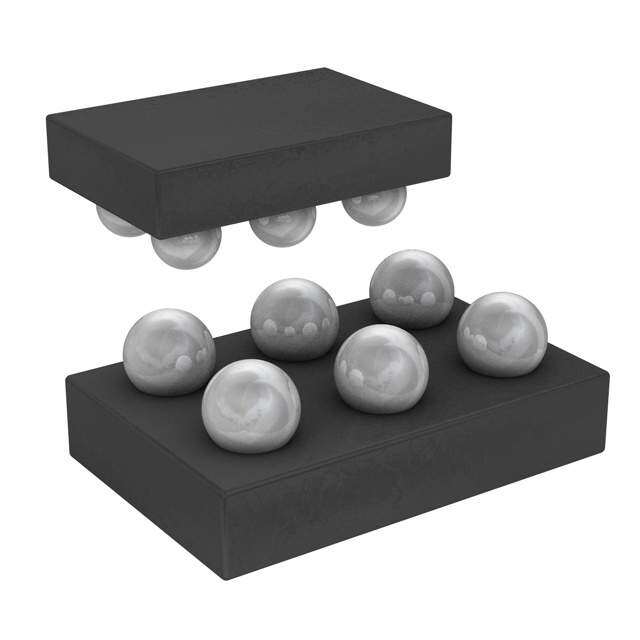
ICGOO在线商城 > 集成电路(IC) > PMIC - 配电开关,负载驱动器 > TPS22951YFPR
- 型号: TPS22951YFPR
- 制造商: Texas Instruments
- 库位|库存: xxxx|xxxx
- 要求:
| 数量阶梯 | 香港交货 | 国内含税 |
| +xxxx | $xxxx | ¥xxxx |
查看当月历史价格
查看今年历史价格
TPS22951YFPR产品简介:
ICGOO电子元器件商城为您提供TPS22951YFPR由Texas Instruments设计生产,在icgoo商城现货销售,并且可以通过原厂、代理商等渠道进行代购。 TPS22951YFPR价格参考¥2.25-¥5.89。Texas InstrumentsTPS22951YFPR封装/规格:PMIC - 配电开关,负载驱动器, Power Switch/Driver 1:1 P-Channel 300mA 6-DSBGA。您可以下载TPS22951YFPR参考资料、Datasheet数据手册功能说明书,资料中有TPS22951YFPR 详细功能的应用电路图电压和使用方法及教程。
| 参数 | 数值 |
| 产品目录 | 集成电路 (IC)半导体 |
| 描述 | IC LOAD SWITCH CURR LIMT 6DSBGA电源开关 IC - 配电 Crnt-Ltd,Pwr-Dist Switch |
| 产品分类 | PMIC - 电源分配开关集成电路 - IC |
| 品牌 | Texas Instruments |
| 产品手册 | |
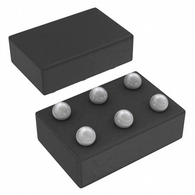
| 产品图片 |
|
| rohs | 符合RoHS无铅 / 符合限制有害物质指令(RoHS)规范要求 |
| 产品系列 | 开关 IC,电源开关 IC - 配电,Texas Instruments TPS22951YFPR- |
| 数据手册 | |
| 产品型号 | TPS22951YFPR |
| Rds(On) | 1 欧姆(最小值) |
| 产品 | Power Switches |
| 产品目录页面 | |
| 产品种类 | Power Muxes and Current Limited Switches |
| 供应商器件封装 | 6-DSBGA |
| 其它名称 | 296-24773-6 |
| 内部开关 | 是 |
| 包装 | Digi-Reel® |
| 商标 | Texas Instruments |
| 安装类型 | 表面贴装 |
| 安装风格 | SMD/SMT |
| 导通电阻—最大值 | 1 Ohms |
| 封装 | Reel |
| 封装/外壳 | 6-XFBGA,DSBGA |
| 封装/箱体 | DSBGA-6 |
| 工作温度 | -40°C ~ 85°C |
| 工作电源电压 | 2.8 V to 5.3 V |
| 工厂包装数量 | 3000 |
| 开关数量 | 1 |
| 开关电流—最大值 | 100 uA |
| 开关类型 | 通用 |
| 最大功率耗散 | 810 mW |
| 最大工作温度 | + 85 C |
| 最大输入电压 | 5.3 V |
| 最小工作温度 | - 40 C |
| 最小输入电压 | 2.8 V |
| 标准包装 | 1 |
| 比率-输入:输出 | 1:1 |
| 特性 | - |
| 电压-负载 | 2.2 V ~ 5.3 V |
| 电压-输入 | 2.2 V ~ 5.3 V |
| 电流-输出(最大值) | 300mA |
| 电流限制 | 600 mA |
| 电源电流 | 100 uA |
| 电源电流—最大值 | 100 uA |
| 类型 | Load Switch |
| 系列 | TPS22951 |
| 输入类型 | - |
| 输出数 | 1 |
| 输出电流 | - 600 mA |
| 输出端数量 | 1 |
| 输出类型 | P 通道 |




- 商务部:美国ITC正式对集成电路等产品启动337调查
- 曝三星4nm工艺存在良率问题 高通将骁龙8 Gen1或转产台积电
- 太阳诱电将投资9.5亿元在常州建新厂生产MLCC 预计2023年完工
- 英特尔发布欧洲新工厂建设计划 深化IDM 2.0 战略
- 台积电先进制程称霸业界 有大客户加持明年业绩稳了
- 达到5530亿美元!SIA预计今年全球半导体销售额将创下新高
- 英特尔拟将自动驾驶子公司Mobileye上市 估值或超500亿美元
- 三星加码芯片和SET,合并消费电子和移动部门,撤换高东真等 CEO
- 三星电子宣布重大人事变动 还合并消费电子和移动部门
- 海关总署:前11个月进口集成电路产品价值2.52万亿元 增长14.8%




PDF Datasheet 数据手册内容提取
Product Sample & Technical Tools & Support & Folder Buy Documents Software Community TPS22951 SLVS788D–FEBRUARY2009–REVISEDNOVEMBER2016 TPS22951 Current-Limited 1-Ω Smart-Load Switch 1 Features 3 Description • 1-Ω P-ChannelMOSFET The TPS22951 smart-load switch is intended for 1 applications where heavy capacitive loads and short • 300-mAContinuousSourceCurrent circuits are likely to be encountered. This device • ThermalandShort-CircuitProtection incorporates a 1-Ω P-channel MOSFET power switch • 600-mACurrentLimit for power distribution. The switch is controlled by a logic enable (EN) input and an accessory detect • OperatingRange:V =2.8Vto5.3V CC (DET) pin. The switch is active when EN is high and • 41-μsTypicalRiseTime DET is low. The switch is disabled if EN is low or • 10-μAMaximumStandbySupplyCurrent DET is high. A low power state is achieved by driving ENlow. • AmbientTemperatureRange:–40°Cto+85°C • ESDPerformanceTestedPerJESD22 When the output load exceeds the current-limit threshold or a short is present, the device limits the – 4000-VHuman-BodyModel(HBM) output current to a safe level by increasing the on – 400-VMachineModel(MM) resistance of the power switch. When continuous – 1000-VCharged-DeviceModel(CDM) heavyoverloadsandshortcircuitsincreasethepower dissipation in the switch, causing the junction 2 Applications temperature to rise, a thermal-protection circuit shuts off the switch to prevent damage. The device • SmartPhones recovers from a thermal shutdown once the device • Notebooks has cooled sufficiently, but the switch remains OFF • DigitalCameras until EN is toggled. This smart-load switch is designedtosetcurrentlimitat600mAmaximum. • PeripheralPorts DeviceInformation(1) PARTNUMBER PACKAGE BODYSIZE(NOM) TPS22951 DSBGA(6) 1.20mmx0.80mm (1) For all available packages, see the orderable addendum at theendofthedatasheet. SimplifiedSchematic Power V PWR Supply CC C C R IN LOAD LOAD ON GND EN OFF VDD PG DET Accessory Detection 1 An IMPORTANT NOTICE at the end of this data sheet addresses availability, warranty, changes, use in safety-critical applications, intellectualpropertymattersandotherimportantdisclaimers.PRODUCTIONDATA.
TPS22951 SLVS788D–FEBRUARY2009–REVISEDNOVEMBER2016 www.ti.com Table of Contents 1 Features.................................................................. 1 8.3 FeatureDescription.................................................10 2 Applications........................................................... 1 8.4 DeviceFunctionalModes........................................10 3 Description............................................................. 1 9 ApplicationandImplementation........................ 11 4 RevisionHistory..................................................... 2 9.1 ApplicationInformation............................................11 9.2 TypicalApplication .................................................11 5 PinConfigurationsandFunctions....................... 3 10 PowerSupplyRecommendations..................... 12 6 Specifications......................................................... 4 11 Layout................................................................... 13 6.1 AbsoluteMaximumRatings .....................................4 6.2 ESDRatings..............................................................4 11.1 LayoutGuidelines.................................................13 6.3 RecommendedOperatingConditions.......................4 11.2 LayoutExample....................................................13 6.4 ThermalInformation..................................................4 11.3 ThermalConsiderations........................................13 6.5 ElectricalCharacteristics...........................................5 12 DeviceandDocumentationSupport................. 15 6.6 TimingRequirements................................................5 12.1 DocumentationSupport........................................15 6.7 SwitchingCharacteristics..........................................5 12.2 ReceivingNotificationofDocumentationUpdates15 6.8 TypicalCharacteristics..............................................6 12.3 CommunityResources..........................................15 7 ParameterMeasurementInformation..................8 12.4 Trademarks...........................................................15 12.5 ElectrostaticDischargeCaution............................15 8 DetailedDescription.............................................. 9 12.6 Glossary................................................................15 8.1 Overview...................................................................9 13 Mechanical,Packaging,andOrderable 8.2 FunctionalBlockDiagram.........................................9 Information........................................................... 15 4 Revision History NOTE:Pagenumbersforpreviousrevisionsmaydifferfrompagenumbersinthecurrentversion. ChangesfromRevisionC(March2015)toRevisionD Page • Changedallinstancesof"POK"to"PG"inthedatasheet.................................................................................................... 1 ChangesfromRevisionB(November2012)toRevisionC Page • AddedPinConfigurationandFunctionssection,ESDRatingstable,FeatureDescriptionsection,DeviceFunctional Modes,ApplicationandImplementationsection,PowerSupplyRecommendationssection,Layoutsection,Device andDocumentationSupportsection,andMechanical,Packaging,andOrderableInformationsection............................... 1 ChangesfromRevisionA(March2009)toRevisionB Page • UpdatedTop-SideMarkingintheOrderingInformationtable................................................................................................ 3 2 SubmitDocumentationFeedback Copyright©2009–2016,TexasInstrumentsIncorporated ProductFolderLinks:TPS22951
TPS22951 www.ti.com SLVS788D–FEBRUARY2009–REVISEDNOVEMBER2016 5 Pin Configurations and Functions YFPPackage 6-PinDSBGA YFPPackage Top-ThroughView 6-PinDSBGA TopView A VCC PWR B GND EN BallA1 IndexArea C PG DET 1 2 PinFunctions Pin I/O DESCRIPTION NO. NAME A1 V I Supplyvoltage CC A2 PWR O Powerswitchoutput B1 GND — Ground B2 EN I Enableinput (1) C1 PG O PowerGoodswitchstatusopen-drainoutput,activelow C2 DET I Accessorydetect,activelow (1) DETmustbelowforaminimumof2μsbeforeENispulledhigh(seetheTimingRequirementssection). Copyright©2009–2016,TexasInstrumentsIncorporated SubmitDocumentationFeedback 3 ProductFolderLinks:TPS22951
TPS22951 SLVS788D–FEBRUARY2009–REVISEDNOVEMBER2016 www.ti.com 6 Specifications 6.1 Absolute Maximum Ratings overoperatingfree-airtemperaturerange(unlessotherwisenoted) (1) MIN MAX UNIT V (2) Supplyvoltage –0.3 6 V CC V (2) Outputvoltage –0.3 V +0.3 V O(PWR) CC V ,V Inputvoltage –0.3 6 V I(EN) I(DET) V Voltage –0.3 6 V O(PG) I Continuousoutputcurrent Internallylimited O(PWR) SeetheThermal Continuoustotalpowerdissipation Informationsection Leadtemperaturesoldering1,6mm(1/16in)fromcasefor10s –0.3 6 V T Operatingvirtualjunctiontemperature –40 85 °C J T Storagetemperature –65 150 °C stg (1) StressesbeyondthoselistedunderAbsoluteMaximumRatingsmaycausepermanentdamagetothedevice.Thesearestressratings only,whichdonotimplyfunctionaloperationofthedeviceattheseoranyotherconditionsbeyondthoseindicatedunderRecommended OperatingConditions.Exposuretoabsolute-maximum-ratedconditionsforextendedperiodsmayaffectdevicereliability. (2) AllvoltagesarewithrespecttoGND. 6.2 ESD Ratings VALUE UNIT Humanbodymodel(HBM),perANSI/ESDA/JEDECJS-001 (1) 4000 Charged-devicemodel(CDM),perJEDECspecificationJESD22-C101 V(ESD) Electrostaticdischarge (2) 1000 V Machinemodel(MM) 400 (1) JEDECdocumentJEP155statesthat500-VHBMallowssafemanufacturingwithastandardESDcontrolprocess. (2) JEDECdocumentJEP157statesthat250-VCDMallowssafemanufacturingwithastandardESDcontrolprocess. 6.3 Recommended Operating Conditions MIN MAX UNIT V Supplyvoltage 2.2 5.3 V CC V ,V Inputvoltage 0 V V I(EN) I(DET) CC I Continuousoutputcurrent 0 –600 mA O(PWR) T Operatingvirtualjunctiontemperature –40 85 °C J 6.4 Thermal Information TPS22951 THERMALMETRIC (1) YFP(DSBGA) UNIT 6PINS R Junction-to-ambientthermalresistance 125.1 °C/W θJA R Junction-to-case(top)thermalresistance 1.4 °C/W θJC(top) R Junction-to-boardthermalresistance 26 °C/W θJB ψ Junction-to-topcharacterizationparameter 0.3 °C/W JT ψ Junction-to-boardcharacterizationparameter 26 °C/W JB R Junction-to-case(bottom)thermalresistance N/A °C/W θJC(bot) (1) Formoreinformationabouttraditionalandnewthermalmetrics,seetheSemiconductorandICPackageThermalMetricsapplication report. 4 SubmitDocumentationFeedback Copyright©2009–2016,TexasInstrumentsIncorporated ProductFolderLinks:TPS22951
TPS22951 www.ti.com SLVS788D–FEBRUARY2009–REVISEDNOVEMBER2016 6.5 Electrical Characteristics overoperating–40°C≤T ≤+85°Crange(unlessotherwisenoted) J PARAMETER TESTCONDITIONS (1) MIN TYP MAX UNIT POWERSWITCH Staticdrain-sourceON-state r V =3V,I =0.3A 1 Ω DS(on) resistance,3-Voperation CC O Leakagecurrent PWRconnectedtoGND,V =0V 1 μA I(EN) ENANDDET V High-levelinputvoltage 2.8V≤V ≤5.3V 1.35 V IH CC V Low-levelinputvoltage 2.8V≤V ≤5.3V 0.45 V IL CC I Inputcurrent V orV =0Vor5.3V 1 μA I I(EN) I(DET) CURRENTLIMIT V =2.8Vor5.3V,PWRconnectedtoGND, I Short-circuitoutputcurrent CC –0.3 –0.6 A OS Deviceenabledintoshortcircuit SUPPLYCURRENT NoloadonPWR,V =5.3V,V =V , Supplycurrent,enabled CC I(EN) CC 100 μA V =V or0V I(DET) CC NoloadonPWR,V =5.3V,V =0V, Supplycurrent,disabled CC I(EN) 10 μA V =V or0V I(DET) CC PG V PowerGoodoutputlowvoltage I =1mA 0.4 V OL(PG) (PG) OFF-statecurrent V =5.3V 1 μA (PG) THERMALSHUTDOWN Thermalshutdownthreshold (2) 135 °C Recoveryfromthermalshutdown (2) 125 °C Hysteresis (2) 25 °C (1) Pulse-testingtechniquesmaintainjunctiontemperatureclosetoambienttemperature;thermaleffectsmustbetakenintoaccount separately. (2) Nottestedinproduction,specifiedbydesign 6.6 Timing Requirements overoperatingfree-airtemperaturerange(unlessotherwisenoted) MIN MAX UNIT t Setuptime,DETlowbeforeENhigh 2 μs su 6.7 Switching Characteristics overoperatingfree-airtemperaturerange(unlessotherwisenoted) PARAMETER TESTCONDITIONS MIN TYP MAX UNIT POWERSWITCH t (1) Risetime,output VCC=5.3V CL=1μF, T =25°C 41 μs r VCC=2.8V RL=20Ω J 6 t (1) Falltime,output VCC=5.3V CL=1μF, T =25°C 43 μs f VCC=2.8V RL=20Ω J 43 ENANDDET Turnontime(ENtoPWR) C =1μF,R =20Ω 42 t (1) V =5.3V L L μs on CC Turnontime(ENtoPG) C =15pF,R =10kΩ 9.5 P P Turnofftime(ENtoPWR) C =1μF,R =20Ω 48 t (1) V =5.3V L L μs off CC Turnofftime(ENtoPG) C =15pF,R =10kΩ 47 P P (1) Nottestedinproduction,specifiedbydesign Copyright©2009–2016,TexasInstrumentsIncorporated SubmitDocumentationFeedback 5 ProductFolderLinks:TPS22951
TPS22951 SLVS788D–FEBRUARY2009–REVISEDNOVEMBER2016 www.ti.com 6.8 Typical Characteristics 800 16 750 14 700 12 DET = HIGH TA=85°C 650 10 TA= 25°C TA= –40°C 600 W) A) 8 (N 550 (C rO IC 6 500 4 450 DET = LOW 400 2 TTAA== 2855°°CC TA= –40°C 350 0 300 –2 2.5 3.0 3.5 4.0 4.5 5.0 5.5 0 1 2 3 4 5 6 VCC(V) VCC(V) Figure1.ON-StateResistancevsVCC Figure2.ICCvsVCC,EN=VCC 6 50 DET = LOW TA=85°C 5 TA= 25°C trise TA= –40°C 40 4 30 I(A)CC3 DETTTAA === H28I55G°°CCH ts)t(mrise/fall 20 tfall 2 TA= –40°C EN = 2V 10 CL=1mF 1 RL= 20W 0 0 0 1 2 3 4 5 6 –50 –25 0 25 50 75 100 VCC(V) Temperature,TA(°C) Figure3.ICCvsVCC,EN=GND Figure4.trise/tfallvsTemperature,VCC=5.3V 60 6 3.0 VON 50 tOFF 5 VIN = 5.3V 2.5 RL= 0W 4 CL= 3mF 2.0 40 tts)(mON/OFF30 tON Voltage (V) 32 11..05 Current (A) 20 IOUT 1 0.5 EN = 2V CL=1mF 10 RL= 20W 0 0.0 0 –1 –0.5 –40 25 85 0.0002 0.0003 0.0004 0.0005 0.0006 0.0007 0.0008 Temperature,TA(°C) Time (s) Figure5.t /t vsTemperature,V =5.3V Figure6.DeviceEnabledintoShort-Circuit ON OFF CC 6 SubmitDocumentationFeedback Copyright©2009–2016,TexasInstrumentsIncorporated ProductFolderLinks:TPS22951
TPS22951 www.ti.com SLVS788D–FEBRUARY2009–REVISEDNOVEMBER2016 Typical Characteristics (continued) 6 1.8 6 4.5 VOUT VIN = 5.3V 1.6 4.0 5 RL= 20Wto 0W 5 CL= 3mF 1.4 3.5 4 1.2 4 VIN = 5.3V 3.0 RL= 20Wto 0W V) 3 1.0A) V) 3 CL= 3mF 2.5A) Voltage ( 2 00..68Current ( Voltage ( 2 21..05Current ( 1 0.4 1 1.0 IOUT 0.2 VOUT IOUT 0.5 0 0 0.0 0.0 –1 –0.2 –1 –0.5 0.0000 0.0002 0.0004 0.0006 0.0008 0.0010 0.0012 0.0000 0.0002 0.0004 0.0006 0.0008 0.0010 0.0012 Time (s) Time (s) Figure7.Full-LoadtoShort-CircuitTransientResponse Figure8.Short-CircuittoFull-LoadRecoveryResponse 6 1.2 VOUT 5 1.0 IOUT 4 0.8 V) 3 0.6A) Voltage ( 2 0.4Current ( 1 0.2 VIN = 5.3V RL= open to 0W 0 CL= 3mF 0.0 –1 –0.2 0.0000 0.0001 0.0002 0.0003 0.0004 0.0005 0.0006 0.0007 0.0008 Time (s) Figure9.No-LoadtoShort-CircuitTransientResponse Copyright©2009–2016,TexasInstrumentsIncorporated SubmitDocumentationFeedback 7 ProductFolderLinks:TPS22951
TPS22951 SLVS788D–FEBRUARY2009–REVISEDNOVEMBER2016 www.ti.com 7 Parameter Measurement Information V O(PWR) R C L L t t r r V O(PWR) 90% 90% TEST CIRCUIT 10% 10% V V I(DET) 50% 50% I(EN) 50% 50% ton toff ton toff V V O(PWR) 90% O(PWR) 90% 10% 10% VOLTAGEWAVEFORMS Figure10. TestCircuitandVoltageWaveforms EN VM= VCC/2 VM= VCC/2 tON tOFF RP VO(PG) VM= VCC/2 VM= VCC/2 CP PG Figure11. ENtoPGTestPoint 8 SubmitDocumentationFeedback Copyright©2009–2016,TexasInstrumentsIncorporated ProductFolderLinks:TPS22951
TPS22951 www.ti.com SLVS788D–FEBRUARY2009–REVISEDNOVEMBER2016 8 Detailed Description 8.1 Overview The TPS22951 smart-load switch is intended for applications where heavy capacitive loads and short circuits are likely to be encountered. This device incorporates a 1-Ω P-channel MOSFET power switch for power distribution. The switch is controlled by a logic enable (EN) input and an accessory detect (DET) pin. The switch is active when EN is high and DET is low. The switch is disabled if EN is low or DET is high. A low power state is achievedbydrivingENlow. Whentheoutputloadexceedsthecurrent-limitthresholdorashortispresent,thedevicelimitstheoutputcurrent to a safe level by increasing the on resistance of the power switch. When continuous heavy overloads and short circuits increase the power dissipation in the switch, causing the junction temperature to rise, a thermal- protection circuit shuts off the switch to prevent damage. The device recovers from a thermal shutdown once the devicehascooledsufficiently,buttheswitchremainsOFFuntilENistoggled.Thissmart-loadswitchisdesigned tosetcurrentlimitat600mAmaximum. 8.2 Functional Block Diagram V CC Die temp Current Detect limit H D Q CP Reset Delay PWR EN PG DET GND Copyright©2009–2016,TexasInstrumentsIncorporated SubmitDocumentationFeedback 9 ProductFolderLinks:TPS22951
TPS22951 SLVS788D–FEBRUARY2009–REVISEDNOVEMBER2016 www.ti.com 8.3 Feature Description 8.3.1 CurrentLimit The TPS22951 includes a current-limiting feature. The current limit can help protect the system from high currents in the case of large capacitive loads and short circuits. When the load current exceeds the current limit threshold,thedevicelimitstheoutputcurrentbyincreasingtheon-resistanceoftheswitch. 8.3.2 PowerGoodIndication The TPS22951 includes an open-drain Power Good indication. This signal can be used to provide an indication toanothercomponentinthesystem.ThesignalbehavesaccordingtoTable1. To use the signal, the PG pin must be connected to a pullup resistor. The PG pin has an absolute maximum rating of 6 V and must not be pulled up to any voltage beyond 6 V. The pullp resistor must be in the range of 10 kΩtolimitthecurrentflowingintothePGpinwhentheswitchisonandthePGsignalislow. 8.3.3 ENandDETinputs TheswitchiscontrolledbytheENandDETpins.Toenabletheswitch,theENpinmustbehighandtheDETpin mustbelow. 8.3.4 ThermalShutdown The TPS22951 includes a thermal shutdown circuit. If the device reaches the thermal shutdown threshold, the switchisautomaticallybedisabled.TheswitchretrysafterthedevicetemperaturehasdecreasedandtheENpin istoggledfromHtoLtoH. 8.4 Device Functional Modes Table1liststhefunctionalmodesoftheTPS22951. Table1.FunctionTable CURRENT THERMAL POWERSWITCH PG EN DET LIMIT LIMIT (V TOPWR) (OPEN-DRAIN) CC 0 X Notexceeded Notexceeded OFF Z X 1 Notexceeded Notexceeded OFF Z 1 0 Notexceeded Notexceeded ON L 1 0 Exceeded Notexceeded ON–current-limited L X X X Exceeded (1) OFF Z (1) Torecoverfromathermalevent,thedietemperaturemustfirstdropbelowthespecifiedlimit.ENmustthenbetoggledtolatchinthe properstateoftheflip-flop. 10 SubmitDocumentationFeedback Copyright©2009–2016,TexasInstrumentsIncorporated ProductFolderLinks:TPS22951
TPS22951 www.ti.com SLVS788D–FEBRUARY2009–REVISEDNOVEMBER2016 9 Application and Implementation NOTE Information in the following applications sections is not part of the TI component specification, and TI does not warrant its accuracy or completeness. TI’s customers are responsible for determining suitability of components for their purposes. Customers should validateandtesttheirdesignimplementationtoconfirmsystemfunctionality. 9.1 Application Information The input to output voltage drop in the device is determined by the R of the device and the load current. The ON R of the device depends upon the V condition of the device. Refer to Figure 1 r vs V to determine the ON CC ON CC r ofthedevicebasedupontheV condition.UseEquation1tocalculatetheinputtooutputvoltagedrop: ON CC DV =I ´R LOAD ON where • ΔV=voltagedropfromV toPWR CC • I =loadcurrent LOAD • R =ON-ResistanceofthedeviceforaspecificV (1) ON CC 9.2 Typical Application This application demonstrates how the TPS22951 can be used to protect against a short-circuit event. In this application,thePWRnodeisaccidentallyshortedtoground. Load #1 Power V PWR Load #2 Supply C CC IN ON GND EN VDD OFF PG DET Figure12. TypicalApplicationCircuit 9.2.1 DesignRequirements Forthisdesignexample,usetheinputparametersgiveninTable2: Table2.DesignParameters DESIGNPARAMTER EXAMPLEVALUE PowerSupplyMaximumDCOutputCurrent 2A Load1CurrentConsumption 1A Copyright©2009–2016,TexasInstrumentsIncorporated SubmitDocumentationFeedback 11 ProductFolderLinks:TPS22951
TPS22951 SLVS788D–FEBRUARY2009–REVISEDNOVEMBER2016 www.ti.com 9.2.2 DetailedDesignProcedure The power supply provides power to multiple loads. In the event that Load 2 is shorted to ground, the power supply must continue providing power to Load 1. The power supply can provide 2-A continuous current. Load 1 consumes 1-A continuous current. The TPS22951 is used to ensure that Load 2 consumes less than 1-A continuous current. This ensures that the power supply can provide power to Load 1 even in the case that Load 2isshortedtoground. 9.2.3 ApplicationCurve 6 3.0 VON 5 VIN = 5.3V 2.5 RL= 0W 4 CL= 3mF 2.0 V) 3 1.5 A) Voltage ( 2 1.0 Current ( IOUT 1 0.5 0 0.0 –1 –0.5 0.0002 0.0003 0.0004 0.0005 0.0006 0.0007 0.0008 Time (s) Figure13. DeviceEnabledintoShort-Circuit 10 Power Supply Recommendations The device is designed to operate from a V range of 2.8 to 5.3 V. The V power supply must be well CC CC regulated and placed as close to the V terminal as possible. The power supply must be able to withstand all CC transient load current steps. In most situations, using a small input capacitor is sufficient to prevent the supply voltagefromdippingwhentheswitchisturnedon.Incaseswherethepowersupplyisslowtorespondtoalarge transientcurrentorlargeloadcurrentstep,additionalbulkcapacitancemayberequiredontheinput. 12 SubmitDocumentationFeedback Copyright©2009–2016,TexasInstrumentsIncorporated ProductFolderLinks:TPS22951
TPS22951 www.ti.com SLVS788D–FEBRUARY2009–REVISEDNOVEMBER2016 11 Layout 11.1 Layout Guidelines • TheV andPWRtracesmustbewideenoughtocarrythenecessaryloadcurrent(upto600mA). CC • Tohandletransientloadcurrents,acapacitormaybeplacedclosetotheV pin. CC • To make use of the PG signal, it must be connected to a pullup resistor. The pullup source may be the V CC node.Itisalsopossibletouseadifferentsourceforthepullupresistor. 11.2 Layout Example V CC PWR GND EN PG DET Via to GND Plane Figure14. LayoutExample 11.3 Thermal Considerations The maximum IC junction temperature must be restricted to 85°C under normal operating conditions. To calculate the maximum allowable dissipation, P for a given ambient temperature, use Equation 2 and D(max) Equation3. T -T P = J(MAX) A D(MAX) R θJA where • P =maximumallowablepowerdissipation D(max) • T =maximumallowablejunctiontemperature(85°CfortheTPS22951) J(max) Copyright©2009–2016,TexasInstrumentsIncorporated SubmitDocumentationFeedback 13 ProductFolderLinks:TPS22951
TPS22951 SLVS788D–FEBRUARY2009–REVISEDNOVEMBER2016 www.ti.com Thermal Considerations (continued) • T =ambienttemperatureofthedevice A • R =junctiontoairthermalimpedance.Seethermalmetricstable.Thisparameterishighlydependentupon θJA boardlayout. (2) P =I2×R (3) D 14 SubmitDocumentationFeedback Copyright©2009–2016,TexasInstrumentsIncorporated ProductFolderLinks:TPS22951
TPS22951 www.ti.com SLVS788D–FEBRUARY2009–REVISEDNOVEMBER2016 12 Device and Documentation Support 12.1 Documentation Support 12.1.1 RelatedDocumentation Forrelateddocumentationseethefollowing: • BasicsofLoadSwitches • LoadSwitchThermalConsiderations 12.2 Receiving Notification of Documentation Updates To receive notification of documentation updates, navigate to the device product folder on ti.com. In the upper right corner, click on Alert me to register and receive a weekly digest of any product information that has changed.Forchangedetails,reviewtherevisionhistoryincludedinanyreviseddocument. 12.3 Community Resources The following links connect to TI community resources. Linked contents are provided "AS IS" by the respective contributors. They do not constitute TI specifications and do not necessarily reflect TI's views; see TI's Terms of Use. TIE2E™OnlineCommunity TI'sEngineer-to-Engineer(E2E)Community.Createdtofostercollaboration amongengineers.Ate2e.ti.com,youcanaskquestions,shareknowledge,exploreideasandhelp solveproblemswithfellowengineers. DesignSupport TI'sDesignSupport QuicklyfindhelpfulE2Eforumsalongwithdesignsupporttoolsand contactinformationfortechnicalsupport. 12.4 Trademarks E2EisatrademarkofTexasInstruments. Allothertrademarksarethepropertyoftheirrespectiveowners. 12.5 Electrostatic Discharge Caution This integrated circuit can be damaged by ESD. Texas Instruments recommends that all integrated circuits be handled with appropriateprecautions.Failuretoobserveproperhandlingandinstallationprocedurescancausedamage. ESDdamagecanrangefromsubtleperformancedegradationtocompletedevicefailure.Precisionintegratedcircuitsmaybemore susceptibletodamagebecauseverysmallparametricchangescouldcausethedevicenottomeetitspublishedspecifications. 12.6 Glossary SLYZ022—TIGlossary. Thisglossarylistsandexplainsterms,acronyms,anddefinitions. 13 Mechanical, Packaging, and Orderable Information The following pages include mechanical, packaging, and orderable information. This information is the most current data available for the designated devices. This data is subject to change without notice and revision of thisdocument.Forbrowser-basedversionsofthisdatasheet,refertotheleft-handnavigation. Copyright©2009–2016,TexasInstrumentsIncorporated SubmitDocumentationFeedback 15 ProductFolderLinks:TPS22951
PACKAGE OPTION ADDENDUM www.ti.com 26-Oct-2016 PACKAGING INFORMATION Orderable Device Status Package Type Package Pins Package Eco Plan Lead/Ball Finish MSL Peak Temp Op Temp (°C) Device Marking Samples (1) Drawing Qty (2) (6) (3) (4/5) TPS22951YFPR ACTIVE DSBGA YFP 6 3000 Green (RoHS SNAGCU Level-1-260C-UNLIM -40 to 85 (2W ~ 2W7) & no Sb/Br) (1) The marketing status values are defined as follows: ACTIVE: Product device recommended for new designs. LIFEBUY: TI has announced that the device will be discontinued, and a lifetime-buy period is in effect. NRND: Not recommended for new designs. Device is in production to support existing customers, but TI does not recommend using this part in a new design. PREVIEW: Device has been announced but is not in production. Samples may or may not be available. OBSOLETE: TI has discontinued the production of the device. (2) Eco Plan - The planned eco-friendly classification: Pb-Free (RoHS), Pb-Free (RoHS Exempt), or Green (RoHS & no Sb/Br) - please check http://www.ti.com/productcontent for the latest availability information and additional product content details. TBD: The Pb-Free/Green conversion plan has not been defined. Pb-Free (RoHS): TI's terms "Lead-Free" or "Pb-Free" mean semiconductor products that are compatible with the current RoHS requirements for all 6 substances, including the requirement that lead not exceed 0.1% by weight in homogeneous materials. Where designed to be soldered at high temperatures, TI Pb-Free products are suitable for use in specified lead-free processes. Pb-Free (RoHS Exempt): This component has a RoHS exemption for either 1) lead-based flip-chip solder bumps used between the die and package, or 2) lead-based die adhesive used between the die and leadframe. The component is otherwise considered Pb-Free (RoHS compatible) as defined above. Green (RoHS & no Sb/Br): TI defines "Green" to mean Pb-Free (RoHS compatible), and free of Bromine (Br) and Antimony (Sb) based flame retardants (Br or Sb do not exceed 0.1% by weight in homogeneous material) (3) MSL, Peak Temp. - The Moisture Sensitivity Level rating according to the JEDEC industry standard classifications, and peak solder temperature. (4) There may be additional marking, which relates to the logo, the lot trace code information, or the environmental category on the device. (5) Multiple Device Markings will be inside parentheses. Only one Device Marking contained in parentheses and separated by a "~" will appear on a device. If a line is indented then it is a continuation of the previous line and the two combined represent the entire Device Marking for that device. (6) Lead/Ball Finish - Orderable Devices may have multiple material finish options. Finish options are separated by a vertical ruled line. Lead/Ball Finish values may wrap to two lines if the finish value exceeds the maximum column width. Important Information and Disclaimer:The information provided on this page represents TI's knowledge and belief as of the date that it is provided. TI bases its knowledge and belief on information provided by third parties, and makes no representation or warranty as to the accuracy of such information. Efforts are underway to better integrate information from third parties. TI has taken and continues to take reasonable steps to provide representative and accurate information but may not have conducted destructive testing or chemical analysis on incoming materials and chemicals. TI and TI suppliers consider certain information to be proprietary, and thus CAS numbers and other limited information may not be available for release. In no event shall TI's liability arising out of such information exceed the total purchase price of the TI part(s) at issue in this document sold by TI to Customer on an annual basis. Addendum-Page 1
PACKAGE OPTION ADDENDUM www.ti.com 26-Oct-2016 Addendum-Page 2
PACKAGE MATERIALS INFORMATION www.ti.com 5-Jan-2019 TAPE AND REEL INFORMATION *Alldimensionsarenominal Device Package Package Pins SPQ Reel Reel A0 B0 K0 P1 W Pin1 Type Drawing Diameter Width (mm) (mm) (mm) (mm) (mm) Quadrant (mm) W1(mm) TPS22951YFPR DSBGA YFP 6 3000 180.0 8.4 0.9 1.3 0.6 4.0 8.0 Q1 PackMaterials-Page1
PACKAGE MATERIALS INFORMATION www.ti.com 5-Jan-2019 *Alldimensionsarenominal Device PackageType PackageDrawing Pins SPQ Length(mm) Width(mm) Height(mm) TPS22951YFPR DSBGA YFP 6 3000 220.0 220.0 34.0 PackMaterials-Page2
PACKAGE OUTLINE YFP0006 DSBGA - 0.5 mm max height SCALE 10.000 DIE SIZE BALL GRID ARRAY B E A BALL A1 CORNER D C 0.5 MAX SEATING PLANE 0.19 0.13 BALL TYP 0.05 C 0.4 TYP SYMM C D: Max = 1.19 mm, Min = 1.13 mm 0.8 TYP B SYMM E: Max = 0.79 mm, Min = 0.73 mm 0.4 TYP A 0.25 6X 0.21 1 2 0.015 C A B 4223410/A 11/2016 NOTES: 1. All linear dimensions are in millimeters. Any dimensions in parenthesis are for reference only. Dimensioning and tolerancing per ASME Y14.5M. 2. This drawing is subject to change without notice. www.ti.com
EXAMPLE BOARD LAYOUT YFP0006 DSBGA - 0.5 mm max height DIE SIZE BALL GRID ARRAY (0.4) TYP 6X ( 0.23) 1 2 A (0.4) TYP B SYMM C SYMM LAND PATTERN EXAMPLE SCALE:50X ( 0.23) 0.05 MAX 0.05 MIN METAL UNDER METAL SOLDER MASK SOLDER MASK ( 0.23) OPENING SOLDER MASK OPENING NON-SOLDER MASK SOLDER MASK DEFINED DEFINED (PREFERRED) SOLDER MASK DETAILS NOT TO SCALE 4223410/A 11/2016 NOTES: (continued) 3. Final dimensions may vary due to manufacturing tolerance considerations and also routing constraints. For more information, see Texas Instruments literature number SNVA009 (www.ti.com/lit/snva009). www.ti.com
EXAMPLE STENCIL DESIGN YFP0006 DSBGA - 0.5 mm max height DIE SIZE BALL GRID ARRAY (0.4) TYP 6X ( 0.25) (R0.05) TYP 1 2 A (0.4) TYP B SYMM METAL TYP C SYMM SOLDER PASTE EXAMPLE BASED ON 0.1 mm THICK STENCIL SCALE:50X 4223410/A 11/2016 NOTES: (continued) 4. Laser cutting apertures with trapezoidal walls and rounded corners may offer better paste release. www.ti.com
IMPORTANTNOTICEANDDISCLAIMER TIPROVIDESTECHNICALANDRELIABILITYDATA(INCLUDINGDATASHEETS),DESIGNRESOURCES(INCLUDINGREFERENCE DESIGNS),APPLICATIONOROTHERDESIGNADVICE,WEBTOOLS,SAFETYINFORMATION,ANDOTHERRESOURCES“ASIS” ANDWITHALLFAULTS,ANDDISCLAIMSALLWARRANTIES,EXPRESSANDIMPLIED,INCLUDINGWITHOUTLIMITATIONANY IMPLIEDWARRANTIESOFMERCHANTABILITY,FITNESSFORAPARTICULARPURPOSEORNON-INFRINGEMENTOFTHIRD PARTYINTELLECTUALPROPERTYRIGHTS. TheseresourcesareintendedforskilleddevelopersdesigningwithTIproducts.Youaresolelyresponsiblefor(1)selectingtheappropriate TIproductsforyourapplication,(2)designing,validatingandtestingyourapplication,and(3)ensuringyourapplicationmeetsapplicable standards,andanyothersafety,security,orotherrequirements.Theseresourcesaresubjecttochangewithoutnotice.TIgrantsyou permissiontousetheseresourcesonlyfordevelopmentofanapplicationthatusestheTIproductsdescribedintheresource.Other reproductionanddisplayoftheseresourcesisprohibited.NolicenseisgrantedtoanyotherTIintellectualpropertyrightortoanythird partyintellectualpropertyright.TIdisclaimsresponsibilityfor,andyouwillfullyindemnifyTIanditsrepresentativesagainst,anyclaims, damages,costs,losses,andliabilitiesarisingoutofyouruseoftheseresources. TI’sproductsareprovidedsubjecttoTI’sTermsofSale(www.ti.com/legal/termsofsale.html)orotherapplicabletermsavailableeitheron ti.comorprovidedinconjunctionwithsuchTIproducts.TI’sprovisionoftheseresourcesdoesnotexpandorotherwisealterTI’sapplicable warrantiesorwarrantydisclaimersforTIproducts. MailingAddress:TexasInstruments,PostOfficeBox655303,Dallas,Texas75265 Copyright©2019,TexasInstrumentsIncorporated
 Datasheet下载

