ICGOO在线商城 > 集成电路(IC) > PMIC - 配电开关,负载驱动器 > TPS22904YFPR
 Datasheet下载
- 型号: TPS22904YFPR
- 制造商: Texas Instruments
- 库位|库存: xxxx|xxxx
- 要求:
| 数量阶梯 | 香港交货 | 国内含税 |
| +xxxx | $xxxx | ¥xxxx |
查看当月历史价格
查看今年历史价格
TPS22904YFPR产品简介:
ICGOO电子元器件商城为您提供TPS22904YFPR由Texas Instruments设计生产,在icgoo商城现货销售,并且可以通过原厂、代理商等渠道进行代购。 TPS22904YFPR价格参考。Texas InstrumentsTPS22904YFPR封装/规格:PMIC - 配电开关,负载驱动器, 。您可以下载TPS22904YFPR参考资料、Datasheet数据手册功能说明书,资料中有TPS22904YFPR 详细功能的应用电路图电压和使用方法及教程。
| 参数 | 数值 |
| 产品目录 | 集成电路 (IC) |
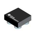
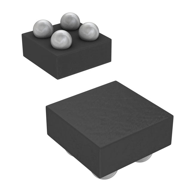
| 描述 | IC LOAD SWITCH USMALL 4DSBGA |
| 产品分类 | PMIC - 电源分配开关 |
| 品牌 | Texas Instruments |
| 数据手册 | |
| 产品图片 |
|
| 产品型号 | TPS22904YFPR |
| PCN组件/产地 | |
| Rds(On) | 66 毫欧 |
| rohs | 无铅 / 符合限制有害物质指令(RoHS)规范要求 |
| 产品系列 | - |
| 供应商器件封装 | 4-DSBGA(0.8x0.8) |
| 其它名称 | 296-27253-1 |
| 内部开关 | 是 |
| 包装 | 剪切带 (CT) |
| 安装类型 | 表面贴装 |
| 封装/外壳 | 4-XFBGA,DSBGA |
| 工作温度 | -40°C ~ 85°C |
| 开关类型 | 通用 |
| 标准包装 | 1 |
| 比率-输入:输出 | 1:1 |
| 特性 | 负载释放,压摆率受控型 |
| 电压-负载 | 1.1 V ~ 3.6 V |
| 电压-输入 | 1.1 V ~ 3.6 V |
| 电流-输出(最大值) | 500mA |
| 电流限制 | 500mA |
| 类型 | 通用 |
| 输入类型 | 非反相 |
| 输出数 | 1 |
| 输出类型 | P 通道 |


- 商务部:美国ITC正式对集成电路等产品启动337调查
- 曝三星4nm工艺存在良率问题 高通将骁龙8 Gen1或转产台积电
- 太阳诱电将投资9.5亿元在常州建新厂生产MLCC 预计2023年完工
- 英特尔发布欧洲新工厂建设计划 深化IDM 2.0 战略
- 台积电先进制程称霸业界 有大客户加持明年业绩稳了
- 达到5530亿美元!SIA预计今年全球半导体销售额将创下新高
- 英特尔拟将自动驾驶子公司Mobileye上市 估值或超500亿美元
- 三星加码芯片和SET,合并消费电子和移动部门,撤换高东真等 CEO
- 三星电子宣布重大人事变动 还合并消费电子和移动部门
- 海关总署:前11个月进口集成电路产品价值2.52万亿元 增长14.8%


PDF Datasheet 数据手册内容提取
Product Sample & Technical Tools & Support & Folder Buy Documents Software Community TPS22903,TPS22904 SLVS827D–FEBRUARY2009–REVISEDJUNE2015 TPS2290x Ultra-Small Low-Input-Voltage Low r Load Switch ON 1 Features 2 Applications • InputVoltage:1.1Vto3.6V • PDAs 1 • UltralowON-StateResistance • CellPhones – r =66mΩ atV =3.6V • GPSDevices ON IN – r =75mΩ atV =2.5V • MP3Players ON IN – r =90mΩ atV =1.8V • DigitalCameras ON IN – r =135mΩatV =1.2V • PeripheralPorts ON IN • 500-mAMaximumContinuousSwitchCurrent • PortableInstrumentation • QuiescentCurrent< 1μA 3 Description • ShutdownCurrent <1 μA The TPS22903 and TPS22904 are ultra-small, low • LowControlInputThresholdEnablesUseof1.2- r single channel load switches with controlled V,1.8-V,2.5-V,and3.3-VLogic ON turnon. The device contains a P-channel MOSFET • ControlledSlewRate(5μsMaximumat3.6V) that can operate over an input voltage range of 1.1 V • QuickOutputDischarge(TPS22904Only) to 3.6 V. The switch is controlled by an on and off input (ON), which is capable of interfacing directly • ESDPerformanceTestedPerJESD22 with low-voltage control signals. In TPS22904, a 85-Ω – 2000-VHumanBodyModel on-chip load resistor is added for output quick (A114-B,ClassII) dischargewhenswitchisturnedoff. – 1000-VCharged-DeviceModel(C101) TPS22903 and TPS22904 are available in a space- • 4-TerminalWaferChip-ScalePackage(WCSP) saving 4-terminal WCSP 0.4-mm pitch (YFP). The devices are characterized for operation over the free- – 0.8mm ×0.8mm, airtemperaturerangeof–40°Cto85°C. 0.4-mmPitch,0.5-mmHeight DeviceInformation(1) PARTNUMBER PACKAGE BODYSIZE(NOM) TPS22903 DSBGA(4) 0.80mm×0.80mm TPS22904 (1) For all available packages, see the orderable addendum at theendofthedatasheet. SimplifiedSchematic VIN VOUT C IN + CL RL - ON ON GND (A) TPS22903 GND OFF GND 1 An IMPORTANT NOTICE at the end of this data sheet addresses availability, warranty, changes, use in safety-critical applications, intellectualpropertymattersandotherimportantdisclaimers.PRODUCTIONDATA.
TPS22903,TPS22904 SLVS827D–FEBRUARY2009–REVISEDJUNE2015 www.ti.com Table of Contents 1 Features.................................................................. 1 9.2 FunctionalBlockDiagram.......................................12 2 Applications........................................................... 1 9.3 FeatureDescription.................................................12 3 Description............................................................. 1 9.4 DeviceFunctionalModes........................................12 4 RevisionHistory..................................................... 2 10 ApplicationandImplementation........................ 13 10.1 ApplicationInformation..........................................13 5 DeviceComparisonTable..................................... 3 10.2 TypicalApplication ...............................................13 6 PinConfigurationandFunctions......................... 3 11 PowerSupplyRecommendations..................... 15 7 Specifications......................................................... 3 12 Layout................................................................... 15 7.1 AbsoluteMaximumRatings......................................3 12.1 LayoutGuidelines.................................................15 7.2 ESDRatings..............................................................4 12.2 LayoutExample....................................................15 7.3 RecommendedOperatingConditions.......................4 13 DeviceandDocumentationSupport................. 16 7.4 ThermalInformation..................................................4 7.5 ElectricalCharacteristics...........................................4 13.1 RelatedLinks........................................................16 7.6 SwitchingCharacteristics..........................................5 13.2 CommunityResources..........................................16 7.7 TypicalCharacteristics..............................................6 13.3 Trademarks...........................................................16 13.4 ElectrostaticDischargeCaution............................16 8 ParameterMeasurementInformation................11 13.5 Glossary................................................................16 9 DetailedDescription............................................ 12 14 Mechanical,Packaging,andOrderable 9.1 Overview.................................................................12 Information........................................................... 16 4 Revision History ChangesfromRevisionC(April2010)toRevisionD Page • AddedPinConfigurationandFunctionssection,ESDRatingstable,FeatureDescriptionsection,DeviceFunctional Modes,ApplicationandImplementationsection,PowerSupplyRecommendationssection,Layoutsection,Device andDocumentationSupportsection,andMechanical,Packaging,andOrderableInformationsection .............................. 1 • RemovedOrderingInformationtable .................................................................................................................................... 1 • RenamedFeatureListtabletoDeviceComparisontable..................................................................................................... 3 2 SubmitDocumentationFeedback Copyright©2009–2015,TexasInstrumentsIncorporated ProductFolderLinks:TPS22903 TPS22904
TPS22903,TPS22904 www.ti.com SLVS827D–FEBRUARY2009–REVISEDJUNE2015 5 Device Comparison Table MAXIMUM r TYPICAL SLEWRATE QUICKOUTPUT DEVICE ONAT3.6V AT3.6V DISCHARGE(1) OUTPUT ENABLE CURRENT TPS22903 66mΩ 5μsmax No 500mA Activehigh TPS22904 66mΩ 5μsmax Yes 500mA Activehigh (1) Thisfeaturedischargestheoutputoftheswitchtogroundthrougha85-Ωresistor,preventingthe outputfromfloating. 6 Pin Configuration and Functions YFPPackage 20-PinDSBGA TopView B B A A 2 1 1 2 Laser MarkingView BumpView PinFunctions PIN I/O DESCRIPTION BALLNO. NAME A1 V I Inputoftheswitch,bypassthisinputwithaceramiccapacitortoground IN A2 V O Outputoftheswitch OUT B1 ON I Switchcontrolinput,activehigh,donotleavefloating B2 GND — Ground 7 Specifications 7.1 Absolute Maximum Ratings overoperatingfree-airtemperaturerange(unlessotherwisenoted)(1) MIN MAX UNIT V Inputvoltage –0.3 4 V IN V Outputvoltage V +0.3 V OUT IN V Inputvoltage –0.3 4 V ON P PowerdissipationatT =25°C 0.48 W D A I Maximumcontinuousswitchcurrent 0.5 A MAX T Operatingfree-airtemperature –40 85 °C A T Maximumleadtemperature(10-ssolderingtime) 300 °C lead T Storagetemperature –65 150 °C stg (1) StressesbeyondthoselistedunderAbsoluteMaximumRatingsmaycausepermanentdamagetothedevice.Thesearestressratings only,whichdonotimplyfunctionaloperationofthedeviceattheseoranyotherconditionsbeyondthoseindicatedunderRecommended OperatingConditions.Exposuretoabsolute-maximum-ratedconditionsforextendedperiodsmayaffectdevicereliability. Copyright©2009–2015,TexasInstrumentsIncorporated SubmitDocumentationFeedback 3 ProductFolderLinks:TPS22903 TPS22904
TPS22903,TPS22904 SLVS827D–FEBRUARY2009–REVISEDJUNE2015 www.ti.com 7.2 ESD Ratings VALUE UNIT Humanbodymodel(HBM),perANSI/ESDA/JEDECJS-001(1) ±2000 V(ESD) Electrostaticdischarge Charged-devicemodel(CDM),perJEDECspecificationJESD22- V C101(2) ±1000 (1) JEDECdocumentJEP155statesthat500-VHBMallowssafemanufacturingwithastandardESDcontrolprocess. (2) JEDECdocumentJEP157statesthat250-VCDMallowssafemanufacturingwithastandardESDcontrolprocess. 7.3 Recommended Operating Conditions overoperatingfree-airtemperaturerange(unlessotherwisenoted) MIN MAX UNIT V Inputvoltage 1.1 3.6 V IN V Outputvoltage V V OUT IN V High-levelinputvoltage,ON 0.85 3.6 V IH V Low-levelinputvoltage,ON 0.4 V IL C Inputcapacitor 1 μF IN 7.4 Thermal Information TPS22903 THERMALMETRIC(1) YFP(DSBGA) UNIT 20PINS R Junction-to-ambientthermalresistance 192.6 °C/W θJA R Junction-to-case(top)thermalresistance 2.3 °C/W θJC(top) R Junction-to-boardthermalresistance 35.8 °C/W θJB ψ Junction-to-topcharacterizationparameter 11.8 °C/W JT ψ Junction-to-boardcharacterizationparameter 35.6 °C/W JB R Junction-to-case(bottom)thermalresistance — °C/W θJC(bot) (1) Formoreinformationabouttraditionalandnewthermalmetrics,seetheSemiconductorandICPackageThermalMetricsapplication report,SPRA953. 7.5 Electrical Characteristics V =1.1Vto3.6V,T =–40°Cto85°C(unlessotherwisenoted) IN A PARAMETER TESTCONDITIONS T MIN TYP(1) MAX UNIT A I Quiescentcurrent I =0,V =V Full 1 μA IN OUT IN ON I OFF-statesupplycurrent V =GND,OUT=Open Full 1 μA IN(OFF) ON I OFF-stateswitchcurrent V =GND,V =0 Full 1 μA IN(LEAKAGE) ON OUT 25°C 66 90 V =3.6V IN Full 95 25°C 75 95 V =2.5V IN Full 110 25°C 90 115 r ON-stateresistance I =–200mA V =1.8V mΩ ON OUT IN Full 125 25°C 135 175 V =1.2V IN Full 185 25°C 157 275 V =1.1V IN Full 300 V =3.3V,V =0(TPS22904only), r Outputpulldownresistance IN ON 85 135 Ω PD I =30mA OUT I ON-stateinputleakagecurrent V =1.1Vto3.6VorGND Full 1 μA ON ON (1) TypicalvaluesareatV =3.3VandT =25°C. IN A 4 SubmitDocumentationFeedback Copyright©2009–2015,TexasInstrumentsIncorporated ProductFolderLinks:TPS22903 TPS22904
TPS22903,TPS22904 www.ti.com SLVS827D–FEBRUARY2009–REVISEDJUNE2015 7.6 Switching Characteristics V =3.6V,T =–40°Cto85°C(unlessotherwisenoted) IN A TPS22903 TPS22904 PARAMETER TESTCONDITIONS UNIT MIN TYP(1) MAX MIN TYP(1) MAX t Turnontime I =100mA,C =0.1μF 0.9 1.5 0.9 1.5 μs ON OUT L t Turnofftime I =100mA,C =0.1μF 5.8 8 5.3 7 μs OFF OUT L t V risetime I =100mA,C =0.1μF 0.80 5 0.8 5 μs r OUT OUT L t V falltime I =100mA,C =0.1μF 8.3 10 5.8 7 μs f OUT OUT L (1) TypicalvaluesareatT =25°C. A Copyright©2009–2015,TexasInstrumentsIncorporated SubmitDocumentationFeedback 5 ProductFolderLinks:TPS22903 TPS22904
TPS22903,TPS22904 SLVS827D–FEBRUARY2009–REVISEDJUNE2015 www.ti.com 7.7 Typical Characteristics 1.0 0.9 0.8 0.7 Ω() ON-State Resistance,rON 000...456 W 0.3 0.2 0.1 0.0 0.7 0.8 0.9 1.0 1.1 1.2 1.3 1.4 1.5 1.6 1.7 1.8 1.9 2.0 2.1 2.2 2.3 2.4 2.5 2.6 2.7 2.8 2.9 3.0 3.1 3.2 3.3 InputVoltage,VIN(V) Temperature (°C) Figure1.rONvsVIN Figure2.rONvsTemperature(VIN=3.3V) 100 200 90 180 80 160 A) 70 (n 140 N mV) 60 VIN= 1.1V ent, II120 Voltage Drop ( 4500 VIN= 1.8VVIN= 1.2V uiescent Curr 18000 V = 2.5V Q 30 IN 60 V = 3.6V IN 20 40 10 20 0 0 0.5 1.0 1.5 2.0 2.5 3.0 3.5 4.0 0 0.05 0.1 0.15 0.2 0.25 0.3 0.35 0.4 0.45 0.5 Load Current (A) InputVoltage,VIN(V) Figure3.VoltageDropvsLoadCurrent Figure4.QuiescentCurrentvsVIN (V =V ,I =0) ON IN OUT 250 120 200 100 A) n ( N urrent, II150 ent (nA) 80 Quiescent C100 ICurrIN(OFF)4600 50 20 0 0 –40 25 85 0.5 1.0 1.5 2.0 2.5 3.0 3.5 4.0 Temperature(°C) InputVoltage,VIN(V) Figure5.QuiescentCurrentvsTemperature Figure6.I vsV (V =0V) IN(OFF) IN ON (V =3.3V,I =0) IN OUT 6 SubmitDocumentationFeedback Copyright©2009–2015,TexasInstrumentsIncorporated ProductFolderLinks:TPS22903 TPS22904
TPS22903,TPS22904 www.ti.com SLVS827D–FEBRUARY2009–REVISEDJUNE2015 Typical Characteristics (continued) 250 120 225 100 200 Current (nA) 111527055 e) Current (nA) 6800 OFF)100 akag IIN( (Le 40 75 IIN 50 20 25 0 0 –40 25 85 0.5 1.0 1.5 2.0 2.5 3.0 3.5 4.0 Temperature(°C) InputVoltage,VIN(V) Figure7.IIN(OFF)vsTemperature(VIN=3.3V) Figure8.IIN(Leakage)vsVIN(IOUT=0) 250 4.0 225 3.5 VIN= 3.6V VIN= 3.3V 200 3.0 VIN= 3V A) 175 n nt ( 2.5 VIN= 2.5V urre 150 eakage) C 110205 V(V)OUT21..05 VINV=IN 1=.5 1V.8V (LN VIN= 1.2V II 75 1.0 VIN= 1.1V 50 0.5 25 0.0 0 –40 25 85 –0.5 0.3 0.4 0.5 0.6 0.7 0.8 Temperature (°C) InputVoltage,VON(V) Figure9. I (Leakage)vsTemperature(V =3.3V) IN IN Figure10.ON-InputThreshold 7 6.0 tfall 5.5 tOFF 6 5.0 4.5 5 4.0 s)m 4 s)m 3.5 ( ( t/tIrisefall 3 CILL== 1 00.01 mµFA t/tONOFF 32..05 CILL== 1 00.01 mµFA 2.0 2 1.5 tON 1 trise 1.0 0.5 0 0.0 –40 –20 0 20 40 60 80 100 –40 –20 0 20 40 60 80 100 Temperature (°C) Temperature (°C) Figure11.t (TPS22903/4)/t (TPS22903)vs Figure12.t (TPS22903/4)/t (TPS22903)vs rise fall ON OFF Temperature(V =3.3V) Temperature(V =3.3V) IN IN Copyright©2009–2015,TexasInstrumentsIncorporated SubmitDocumentationFeedback 7 ProductFolderLinks:TPS22903 TPS22904
TPS22903,TPS22904 SLVS827D–FEBRUARY2009–REVISEDJUNE2015 www.ti.com Typical Characteristics (continued) 6 6 t fall 5 5.5 4 CL= 0.1 µF CL= 0.1 µF IL= 100 mA IL= 100 mA (µs) 3 (µs) 5 tfall tOFF tOFF 2 4.5 1 0 -40 -20 0 20 40 60 80 100 4 -40 -20 0 20 40 60 80 100 Temperature (°C) Temperature (°C) Figure13.t (TPS22904)vsTemperature(V =3.3V) fall IN Figure14.t (TPS22904)vsTemperature(V =3.3V) OFF IN VON VON 200 mV/DIV 200 mV/DIV CL= 0.1mF CL= 10mF IOUT= 100 mA IOUT= 100 mA IOUT VIN= 1.2V IOUT VIN= 1.2V 20 mA/DIV 20 mA/DIV 5ms/DIV 20ms/DIV Figure15.t Response Figure16.t Response ON ON VON VON 200 mV/DIV 200 mV/DIV CL= 0.1mF CL= 10mF IOUT= 100 mA IOUT= 100 mA IOUT VIN= 3.3V IOUT VIN= 3.3V 20 mA/DIV 20 mA/DIV 5ms/DIV 20ms/DIV Figure17.t Response Figure18.t Response ON ON 8 SubmitDocumentationFeedback Copyright©2009–2015,TexasInstrumentsIncorporated ProductFolderLinks:TPS22903 TPS22904
TPS22903,TPS22904 www.ti.com SLVS827D–FEBRUARY2009–REVISEDJUNE2015 Typical Characteristics (continued) CL= 0.1mF CL= 10mF IOUT= 100 mA IOUT= 100 mA VIN= 1.2V VIN= 1.2V VON VON 200 mV/DIV 200 mV/DIV IOUT IOUT 20 mA/DIV 20 mA/DIV 2ms/DIV 100ms/DIV Figure19.tOFFResponse(TPS22903) Figure20.tOFFResponse(TPS22903) CL= 0.1mF CL= 10mF IOUT= 100 mA IOUT= 100 mA VIN= 3.3V VIN= 3.3V VON VON 200 mV/DIV 200 mV/DIV IOUT IOUT 20 mA/DIV 20 mA/DIV 5ms/DIV 200ms/DIV Figure21.t Response(TPS22903) Figure22.t Response(TPS22903) OFF OFF VON VON 200 mV/DIV 200 mV/DIV IOUT IOUT 20 mA/DIV 20 mA/DIV CL= 0.1mF CL= 0.1mF IOUT= 100 mA IOUT= 100 mA VIN= 3.3V VIN= 1.2V 2ms/DIV 5ms/DIV Figure23.tOFFResponse(TPS22904) Figure24.tOFFResponse(TPS22904) Copyright©2009–2015,TexasInstrumentsIncorporated SubmitDocumentationFeedback 9 ProductFolderLinks:TPS22903 TPS22904
TPS22903,TPS22904 SLVS827D–FEBRUARY2009–REVISEDJUNE2015 www.ti.com Typical Characteristics (continued) VON VON 200 mV/DIV 200 mV/DIV IOUT IOUT 20 mA/DIV 20 mA/DIV CL= 10mF CL= 10mF IOUT= 100 mA IOUT= 100 mA VIN= 1.2V VIN= 3.3V 100ms/DIV 200ms/DIV Figure25.t Response(TPS22904) Figure26.t Response(TPS22904) OFF OFF 10 SubmitDocumentationFeedback Copyright©2009–2015,TexasInstrumentsIncorporated ProductFolderLinks:TPS22903 TPS22904
TPS22903,TPS22904 www.ti.com SLVS827D–FEBRUARY2009–REVISEDJUNE2015 8 Parameter Measurement Information V IN V OUT ON(A) C R L L + TPS22903 OFF – C =10 x C IN L GND GND GND TEST CIRCUIT 1.8V V ON VON VON/2 VON/2 tr tf 0V 0V t t ON OFF V 90% 90% OUT VOH 10% 10% V V /2 V /2 OUT OUT OUT V OL t /t WAVEFORMS ON OFF A. t andt ofthecontrolsignalis100ns. rise fall Figure27. TestCircuitandt /t Waveforms ON OFF Copyright©2009–2015,TexasInstrumentsIncorporated SubmitDocumentationFeedback 11 ProductFolderLinks:TPS22903 TPS22904
TPS22903,TPS22904 SLVS827D–FEBRUARY2009–REVISEDJUNE2015 www.ti.com 9 Detailed Description 9.1 Overview TheTPS22903andTPS22904aresingle-channelloadswitcheswithcontrolledturnon. The devices contain a P-channel MOSFET that can operate over an input voltage range of 1.1 V to 3.6 V. The switch is controlled by an on and off input (ON), which is capable of interfacing directly with low-voltage control signals. In TPS22904, a 85-Ω on-chip load resistor is added for output quick discharge when switch is turned off. Bothdevicesareavailableinaspace-saving4-terminalWCSP0.4-mmpitch(YFP). 9.2 Functional Block Diagram VIN A1 Turn-OnSlewRate ControlledDriver ON B1 Control Logic A2 VOUT ESD Protection Output Discharge TPS22904 Only B2 GND 9.3 Feature Description 9.3.1 ON/OFFControl The ON pin controls the state of the switch. Activating ON continuously holds the switch in the ON-state as there is no fault. ON is active-high and has a low threshold, making it capable of interfacing with low voltage signals. The ON pin is compatible with standard GPIO logic thresholds. It can be used with any microcontroller with 1.2- V,1.8-V,2.5-V,or3.3-VGPIOs. 9.4 Device Functional Modes Table1liststheVOUTpinconnectionsasdeterminedbytheONpin. Table1.FunctionalTable ON V TOGND V TOV OUT (CONTROLINPUT) IN OUT (TPS22904ONLY) L OFF ON H ON OFF 12 SubmitDocumentationFeedback Copyright©2009–2015,TexasInstrumentsIncorporated ProductFolderLinks:TPS22903 TPS22904
TPS22903,TPS22904 www.ti.com SLVS827D–FEBRUARY2009–REVISEDJUNE2015 10 Application and Implementation NOTE Information in the following applications sections is not part of the TI component specification, and TI does not warrant its accuracy or completeness. TI’s customers are responsible for determining suitability of components for their purposes. Customers should validateandtesttheirdesignimplementationtoconfirmsystemfunctionality. 10.1 Application Information 10.1.1 InputCapacitor(Optional) To limit the voltage drop on the input supply caused by transient in-rush currents when the switch turns on into a discharged load capacitor or short-circuit, a capacitor needs to be placed between V and GND. A 1-μF ceramic IN capacitor, C , placed close to the pins, is usually sufficient. Higher values of C can be used to further reduce IN IN the voltage drop during high-current application. When switching heavy loads, TI recommends to have an input capacitorabout10timeshigherthantheoutputcapacitortoavoidexcessivevoltagedrop. 10.1.2 OutputCapacitor(Optional) Due to the integral body diode in the PMOS switch, a C greater than C is highly recommended. A C greater IN L L than C can cause V to exceed V when the system supply is removed. This could result in current flow IN OUT IN throughthebodydiodefromV toV . OUT IN 10.2 Typical Application VIN VOUT C IN + CL RL - ON ON GND (A) TPS22903 GND OFF GND Figure28. TypicalApplicationSchematic 10.2.1 DesignRequirements Table2liststhedesignparametersfortheTPS22903device. Table2.DesignParameters DESIGNPARAMETER EXAMPLEVALUE VIN 1.8V LoadCurrent 0.3A AmbientTemperature 25°C 10.2.2 DetailedDesignProcedure 10.2.2.1 VINtoVOUTVoltageDrop The voltage drop from VIN to VOUT is determined by the ON-resistance of the device and the load current. RON can be found in Electrical Characteristics and is dependent on temperature. When the value of RON is found, Equation1canbeusedtocalculatethevoltagedropacrossthedevice: ΔV=I ×R LOAD ON where Copyright©2009–2015,TexasInstrumentsIncorporated SubmitDocumentationFeedback 13 ProductFolderLinks:TPS22903 TPS22904
TPS22903,TPS22904 SLVS827D–FEBRUARY2009–REVISEDJUNE2015 www.ti.com • ΔV=Voltagedropacrossthedevice • I =Loadcurrent LOAD • R =ON-resistanceofthedevice (1) ON At VIN = 1.8 V, the TPS22903/4 has an RON value of 90 mΩ. Using this value and the defined load current, the aboveequationcanbeevaluated: ΔV=0.30A×90mΩ where • ΔV=27mV (2) Therefore,thevoltagedropacrossthedevicewillbe27mV. 10.2.3 ApplicationCurve Figure29showstheexpectedvoltagedropacrossthedevicefordifferentloadcurrentsandinputvoltages. 100 90 80 70 V) 60 VIN= 1.1V m p ( Dro 50 VIN= 1.2V e g a V = 1.8V olt 40 IN V V = 2.5V IN 30 V = 3.6V IN 20 10 0 0 0.05 0.1 0.15 0.2 0.25 0.3 0.35 0.4 0.45 0.5 Load Current (A) Figure29. VoltageDropvsLoadCurrent 14 SubmitDocumentationFeedback Copyright©2009–2015,TexasInstrumentsIncorporated ProductFolderLinks:TPS22903 TPS22904
TPS22903,TPS22904 www.ti.com SLVS827D–FEBRUARY2009–REVISEDJUNE2015 11 Power Supply Recommendations The device is designed to operate with a VIN range of 1.1 V to 3.6 V. This supply must be well regulated and placed as close to the device terminals as possible. It must also be able to withstand all transient and load currents, using a recommended input capacitance of 1 μF if necessary. If the supply is more than a few inches from the device terminals, additional bulk capacitance may be required in addition to the ceramic bypass capacitors. If additional bulk capacitance is required, an electrolytic, tantalum, or ceramic capacitor of 10 μF may besufficient. 12 Layout 12.1 Layout Guidelines For best performance, all traces should be as short as possible. To be most effective, the input and output capacitors should be placed close to the device to minimize the effects that parasitic trace inductances may have on normal and short-circuit operation. Using wide traces for V , V , and GND helps minimize the parasitic IN OUT electricaleffectsalongwithminimizingthecase-to-ambientthermalimpedance. 12.2 Layout Example To GPIO Control GND ON V Bypass VOUT VIN OUT Capacitor V Bypass IN Capacitor VIA Power Ground Plane Figure30. LayoutExampleRecommendation Copyright©2009–2015,TexasInstrumentsIncorporated SubmitDocumentationFeedback 15 ProductFolderLinks:TPS22903 TPS22904
TPS22903,TPS22904 SLVS827D–FEBRUARY2009–REVISEDJUNE2015 www.ti.com 13 Device and Documentation Support 13.1 Related Links The table below lists quick access links. Categories include technical documents, support and community resources,toolsandsoftware,andquickaccesstosampleorbuy. Table3.RelatedLinks TECHNICAL TOOLS& SUPPORT& PARTS PRODUCTFOLDER SAMPLE&BUY DOCUMENTS SOFTWARE COMMUNITY TPS22903 Clickhere Clickhere Clickhere Clickhere Clickhere TPS22904 Clickhere Clickhere Clickhere Clickhere Clickhere 13.2 Community Resources The following links connect to TI community resources. Linked contents are provided "AS IS" by the respective contributors. They do not constitute TI specifications and do not necessarily reflect TI's views; see TI's Terms of Use. TIE2E™OnlineCommunity TI'sEngineer-to-Engineer(E2E)Community.Createdtofostercollaboration amongengineers.Ate2e.ti.com,youcanaskquestions,shareknowledge,exploreideasandhelp solveproblemswithfellowengineers. DesignSupport TI'sDesignSupport QuicklyfindhelpfulE2Eforumsalongwithdesignsupporttoolsand contactinformationfortechnicalsupport. 13.3 Trademarks E2EisatrademarkofTexasInstruments. Allothertrademarksarethepropertyoftheirrespectiveowners. 13.4 Electrostatic Discharge Caution Thesedeviceshavelimitedbuilt-inESDprotection.Theleadsshouldbeshortedtogetherorthedeviceplacedinconductivefoam duringstorageorhandlingtopreventelectrostaticdamagetotheMOSgates. 13.5 Glossary SLYZ022—TIGlossary. Thisglossarylistsandexplainsterms,acronyms,anddefinitions. 14 Mechanical, Packaging, and Orderable Information The following pages include mechanical, packaging, and orderable information. This information is the most current data available for the designated devices. This data is subject to change without notice and revision of thisdocument.Forbrowser-basedversionsofthisdatasheet,refertotheleft-handnavigation. 16 SubmitDocumentationFeedback Copyright©2009–2015,TexasInstrumentsIncorporated ProductFolderLinks:TPS22903 TPS22904
PACKAGE OPTION ADDENDUM www.ti.com 7-Jun-2017 PACKAGING INFORMATION Orderable Device Status Package Type Package Pins Package Eco Plan Lead/Ball Finish MSL Peak Temp Op Temp (°C) Device Marking Samples (1) Drawing Qty (2) (6) (3) (4/5) TPS22903YFPR NRND DSBGA YFP 4 3000 Green (RoHS SNAGCU Level-1-260C-UNLIM -40 to 85 4P & no Sb/Br) (2 ~ N) TPS22904YFPR ACTIVE DSBGA YFP 4 3000 Green (RoHS SNAGCU Level-1-260C-UNLIM -40 to 85 4R & no Sb/Br) (2 ~ N) TPS22904YFPT ACTIVE DSBGA YFP 4 250 Green (RoHS SNAGCU Level-1-260C-UNLIM -40 to 85 4R & no Sb/Br) (2 ~ N) (1) The marketing status values are defined as follows: ACTIVE: Product device recommended for new designs. LIFEBUY: TI has announced that the device will be discontinued, and a lifetime-buy period is in effect. NRND: Not recommended for new designs. Device is in production to support existing customers, but TI does not recommend using this part in a new design. PREVIEW: Device has been announced but is not in production. Samples may or may not be available. OBSOLETE: TI has discontinued the production of the device. (2) RoHS: TI defines "RoHS" to mean semiconductor products that are compliant with the current EU RoHS requirements for all 10 RoHS substances, including the requirement that RoHS substance do not exceed 0.1% by weight in homogeneous materials. Where designed to be soldered at high temperatures, "RoHS" products are suitable for use in specified lead-free processes. TI may reference these types of products as "Pb-Free". RoHS Exempt: TI defines "RoHS Exempt" to mean products that contain lead but are compliant with EU RoHS pursuant to a specific EU RoHS exemption. Green: TI defines "Green" to mean the content of Chlorine (Cl) and Bromine (Br) based flame retardants meet JS709B low halogen requirements of <=1000ppm threshold. Antimony trioxide based flame retardants must also meet the <=1000ppm threshold requirement. (3) MSL, Peak Temp. - The Moisture Sensitivity Level rating according to the JEDEC industry standard classifications, and peak solder temperature. (4) There may be additional marking, which relates to the logo, the lot trace code information, or the environmental category on the device. (5) Multiple Device Markings will be inside parentheses. Only one Device Marking contained in parentheses and separated by a "~" will appear on a device. If a line is indented then it is a continuation of the previous line and the two combined represent the entire Device Marking for that device. (6) Lead/Ball Finish - Orderable Devices may have multiple material finish options. Finish options are separated by a vertical ruled line. Lead/Ball Finish values may wrap to two lines if the finish value exceeds the maximum column width. Important Information and Disclaimer:The information provided on this page represents TI's knowledge and belief as of the date that it is provided. TI bases its knowledge and belief on information provided by third parties, and makes no representation or warranty as to the accuracy of such information. Efforts are underway to better integrate information from third parties. TI has taken and continues to take reasonable steps to provide representative and accurate information but may not have conducted destructive testing or chemical analysis on incoming materials and chemicals. TI and TI suppliers consider certain information to be proprietary, and thus CAS numbers and other limited information may not be available for release. Addendum-Page 1
PACKAGE OPTION ADDENDUM www.ti.com 7-Jun-2017 In no event shall TI's liability arising out of such information exceed the total purchase price of the TI part(s) at issue in this document sold by TI to Customer on an annual basis. Addendum-Page 2
PACKAGE MATERIALS INFORMATION www.ti.com 18-Jan-2020 TAPE AND REEL INFORMATION *Alldimensionsarenominal Device Package Package Pins SPQ Reel Reel A0 B0 K0 P1 W Pin1 Type Drawing Diameter Width (mm) (mm) (mm) (mm) (mm) Quadrant (mm) W1(mm) TPS22903YFPR DSBGA YFP 4 3000 178.0 9.2 0.89 0.89 0.58 4.0 8.0 Q1 TPS22904YFPR DSBGA YFP 4 3000 178.0 9.2 0.89 0.89 0.58 4.0 8.0 Q1 TPS22904YFPT DSBGA YFP 4 250 178.0 9.2 0.89 0.89 0.58 4.0 8.0 Q1 PackMaterials-Page1
PACKAGE MATERIALS INFORMATION www.ti.com 18-Jan-2020 *Alldimensionsarenominal Device PackageType PackageDrawing Pins SPQ Length(mm) Width(mm) Height(mm) TPS22903YFPR DSBGA YFP 4 3000 220.0 220.0 35.0 TPS22904YFPR DSBGA YFP 4 3000 220.0 220.0 35.0 TPS22904YFPT DSBGA YFP 4 250 220.0 220.0 35.0 PackMaterials-Page2
PACKAGE OUTLINE YFP0004 DSBGA - 0.5 mm max height SCALE 10.000 DIE SIZE BALL GRID ARRAY B E A BALL A1 CORNER D C 0.5 MAX SEATING PLANE 0.19 0.13 BALL TYP 0.05 C 0.4 TYP B D: Max = 0.79 mm, Min = 0.73 mm SYMM 0.4 E: Max = 0.79 mm, Min = 0.73 mm TYP A 0.25 4X 0.21 1 2 0.015 C A B SYMM 4223507/A 01/2017 NOTES: 1. All linear dimensions are in millimeters. Any dimensions in parenthesis are for reference only. Dimensioning and tolerancing per ASME Y14.5M. 2. This drawing is subject to change without notice. www.ti.com
EXAMPLE BOARD LAYOUT YFP0004 DSBGA - 0.5 mm max height DIE SIZE BALL GRID ARRAY (0.4) TYP 4X ( 0.23) 1 2 A SYMM (0.4) TYP B SYMM LAND PATTERN EXAMPLE EXPOSED METAL SHOWN SCALE:50X ( 0.23) 0.05 MAX 0.05 MIN METAL UNDER METAL SOLDER MASK EXPOSED SOLDER MASK EXPOSED ( 0.23) METAL OPENING METAL SOLDER MASK OPENING NON-SOLDER MASK SOLDER MASK DEFINED DEFINED (PREFERRED) SOLDER MASK DETAILS NOT TO SCALE 4223507/A 01/2017 NOTES: (continued) 3. Final dimensions may vary due to manufacturing tolerance considerations and also routing constraints. For more information, see Texas Instruments literature number SNVA009 (www.ti.com/lit/snva009). www.ti.com
EXAMPLE STENCIL DESIGN YFP0004 DSBGA - 0.5 mm max height DIE SIZE BALL GRID ARRAY (0.4) TYP 4X ( 0.25) (R0.05) TYP 1 2 A SYMM (0.4) TYP B METAL TYP SYMM SOLDER PASTE EXAMPLE BASED ON 0.1 mm THICK STENCIL SCALE:50X 4223507/A 01/2017 NOTES: (continued) 4. Laser cutting apertures with trapezoidal walls and rounded corners may offer better paste release. www.ti.com
IMPORTANTNOTICEANDDISCLAIMER TI PROVIDES TECHNICAL AND RELIABILITY DATA (INCLUDING DATASHEETS), DESIGN RESOURCES (INCLUDING REFERENCE DESIGNS), APPLICATION OR OTHER DESIGN ADVICE, WEB TOOLS, SAFETY INFORMATION, AND OTHER RESOURCES “AS IS” AND WITH ALL FAULTS, AND DISCLAIMS ALL WARRANTIES, EXPRESS AND IMPLIED, INCLUDING WITHOUT LIMITATION ANY IMPLIED WARRANTIES OF MERCHANTABILITY, FITNESS FOR A PARTICULAR PURPOSE OR NON-INFRINGEMENT OF THIRD PARTY INTELLECTUAL PROPERTY RIGHTS. These resources are intended for skilled developers designing with TI products. You are solely responsible for (1) selecting the appropriate TI products for your application, (2) designing, validating and testing your application, and (3) ensuring your application meets applicable standards, and any other safety, security, or other requirements. These resources are subject to change without notice. TI grants you permission to use these resources only for development of an application that uses the TI products described in the resource. Other reproduction and display of these resources is prohibited. No license is granted to any other TI intellectual property right or to any third party intellectual property right. TI disclaims responsibility for, and you will fully indemnify TI and its representatives against, any claims, damages, costs, losses, and liabilities arising out of your use of these resources. TI’s products are provided subject to TI’s Terms of Sale (www.ti.com/legal/termsofsale.html) or other applicable terms available either on ti.com or provided in conjunction with such TI products. TI’s provision of these resources does not expand or otherwise alter TI’s applicable warranties or warranty disclaimers for TI products. Mailing Address: Texas Instruments, Post Office Box 655303, Dallas, Texas 75265 Copyright © 2020, Texas Instruments Incorporated