ICGOO在线商城 > 集成电路(IC) > PMIC - 配电开关,负载驱动器 > TPS2065DGNR

 Datasheet下载
- 型号: TPS2065DGNR
- 制造商: Texas Instruments
- 库位|库存: xxxx|xxxx
- 要求:
| 数量阶梯 | 香港交货 | 国内含税 |
| +xxxx | $xxxx | ¥xxxx |
查看当月历史价格
查看今年历史价格
TPS2065DGNR产品简介:
ICGOO电子元器件商城为您提供TPS2065DGNR由Texas Instruments设计生产,在icgoo商城现货销售,并且可以通过原厂、代理商等渠道进行代购。 TPS2065DGNR价格参考。Texas InstrumentsTPS2065DGNR封装/规格:PMIC - 配电开关,负载驱动器, 。您可以下载TPS2065DGNR参考资料、Datasheet数据手册功能说明书,资料中有TPS2065DGNR 详细功能的应用电路图电压和使用方法及教程。
TPS2065DGNR 是 Texas Instruments(德州仪器)推出的一款 PMIC(电源管理集成电路),属于配电开关和负载驱动器类别。该型号的主要应用场景如下:

1. 便携式电子设备:TPS2065DGNR 适用于需要高效电源管理和低功耗的便携式设备,例如智能手机、平板电脑、笔记本电脑和其他手持式电子产品。其小型封装和低静态电流特性使其非常适合对空间和电池寿命要求较高的应用。

2. USB 端口保护与控制:该器件常用于 USB 端口的电源分配和保护,能够提供过流保护、短路保护以及热关断功能,确保 USB 设备的安全运行。它支持高达 3A 的负载电流,适合为外接设备供电。

3. 工业自动化系统:在工业领域中,TPS2065DGNR 可用于分布式电源系统的负载开关管理,帮助实现精确的负载控制和故障检测。例如,在 PLC(可编程逻辑控制器)、传感器模块或数据采集系统中,它可以用来隔离和保护关键电路。

4. 通信设备:此 IC 广泛应用于路由器、交换机、基站等通信设备中,用作子系统的电源分配和保护。通过快速响应瞬态事件,它能有效防止因异常情况导致的硬件损坏。

5. 消费类电子产品:包括数码相机、游戏机、音频播放器等在内的各种消费类电子产品均可采用 TPS2065DGNR 来优化电源管理方案,提升产品性能并延长使用寿命。

6. 汽车电子系统(非核心安全区域):虽然 TPS2065DGNR 不专门针对汽车级应用设计,但在某些非关键性车载电子部件中(如信息娱乐系统、导航设备等),也可以利用其特性来简化电源架构。

总之,TPS2065DGNR 凭借其高可靠性、灵活性及易用性,在众多需要精准控制电源分配和保护的应用场景中发挥重要作用。
| 参数 | 数值 |
| 产品目录 | 集成电路 (IC)半导体 |
| 描述 | IC 1.5A POWER DIST SW 8-MSOPUSB开关IC Sngl 1A Crnt-Lit Pwr-Dstibtn Switches |
| 产品分类 | PMIC - 电源分配开关集成电路 - IC |
| 品牌 | Texas Instruments |
| 产品手册 | |
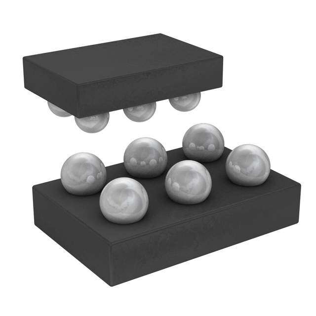
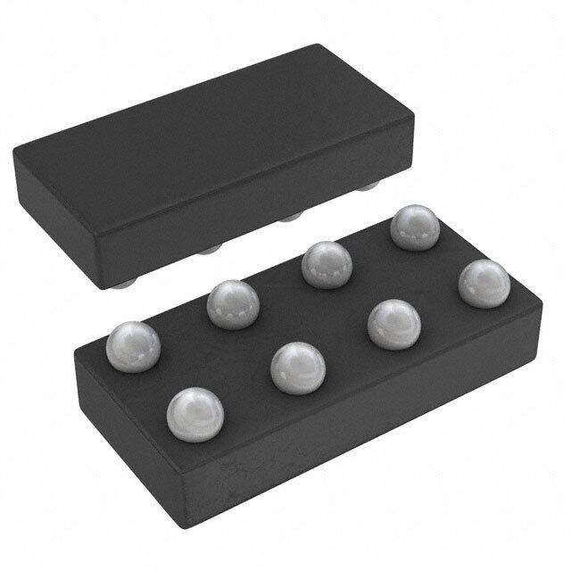
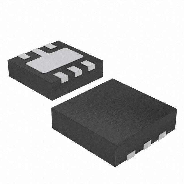
| 产品图片 |
|
| rohs | 符合RoHS无铅 / 符合限制有害物质指令(RoHS)规范要求 |
| 产品系列 | 开关 IC,USB开关IC,Texas Instruments TPS2065DGNR- |
| 数据手册 | |
| 产品型号 | TPS2065DGNR |
| Rds(On) | 70 毫欧 |
| 产品种类 | USB开关IC |
| 供应商器件封装 | 8-MSOP-PowerPad |
| 其它名称 | 296-17314-1 |
| 内部开关 | 是 |
| 包装 | 剪切带 (CT) |
| 商标 | Texas Instruments |
| 安装类型 | 表面贴装 |
| 安装风格 | SMD/SMT |
| 封装 | Reel |
| 封装/外壳 | 8-TSSOP,8-MSOP(0.118",3.00mm 宽)裸焊盘 |
| 封装/箱体 | HVSSOP-8 |
| 工作温度 | -40°C ~ 85°C |
| 工作温度范围 | - 40 C to + 85 C |
| 工厂包装数量 | 2500 |
| 开关数量 | Single |
| 开关类型 | 通用 |
| 接口 | 开/关 |
| 最大功率耗散 | 1712.3 mW |
| 最大工作温度 | + 85 C |
| 最小工作温度 | - 40 C |
| 标准包装 | 1 |
| 比率-输入:输出 | 1:1 |
| 特性 | - |
| 电压-电源(Vcc/Vdd) | 不需要 |
| 电压-负载 | 2.7 V ~ 5.5 V |
| 电压-输入 | 2.7 V ~ 5.5 V |
| 电流-输出(最大值) | 1A |
| 电流限制 | 1.5A |
| 电源电压-最大 | 5.5 V |
| 电源电压-最小 | 2.7 V |
| 空闲时间—最大值 | 10 ms |
| 类型 | USB 开关 |
| 系列 | TPS2065 |
| 输入类型 | 非反相 |
| 输出数 | 1 |
| 输出类型 | N 通道 |
| 输出配置 | 高端 |
| 运行时间—最大值 | 3 ms |
| 配用 | /product-detail/zh/TPS2065-1EVM-292/TPS2065-1EVM-292-ND/1907623/product-detail/zh/TPS2065EVM-290/TPS2065EVM-290-ND/1907627/product-detail/zh/TPS2065EVM-292/TPS2065EVM-292-ND/1907628 |


- 商务部:美国ITC正式对集成电路等产品启动337调查
- 曝三星4nm工艺存在良率问题 高通将骁龙8 Gen1或转产台积电
- 太阳诱电将投资9.5亿元在常州建新厂生产MLCC 预计2023年完工
- 英特尔发布欧洲新工厂建设计划 深化IDM 2.0 战略
- 台积电先进制程称霸业界 有大客户加持明年业绩稳了
- 达到5530亿美元!SIA预计今年全球半导体销售额将创下新高
- 英特尔拟将自动驾驶子公司Mobileye上市 估值或超500亿美元
- 三星加码芯片和SET,合并消费电子和移动部门,撤换高东真等 CEO
- 三星电子宣布重大人事变动 还合并消费电子和移动部门
- 海关总署:前11个月进口集成电路产品价值2.52万亿元 增长14.8%


PDF Datasheet 数据手册内容提取
TPS2061, TPS2062, TPS2063 TPS2065, TPS2066, TPS2067 www.ti.com SLVS490I–DECEMBER2003–REVISEDOCTOBER2009 CURRENT-LIMITED, POWER-DISTRIBUTION SWITCHES CheckforSamples:TPS2061 TPS2062 TPS2063TPS2065 TPS2066 TPS2067 FEATURES APPLICATIONS 1 • 70-mΩ High-SideMOSFET • HeavyCapacitiveLoads 2 • 1-AContinuousCurrent • Short-CircuitProtections • ThermalandShort-CircuitProtection TPS2061/TPS2065 TPS2062/TPS2066 DAND DGN PACKAGE DAND DGN PACKAGE • AccurateCurrentLimit (TOPVIEW) (TOPVIEW) (1.1Amin,1.9Amax) GND 1 8 OUT GND 1 8 OC1 IN 2 7 OUT IN 2 7 OUT1 • OperatingRange:2.7Vto5.5V IN 3 6 OUT EN1† 3 6 OUT2 • 0.6-msTypicalRiseTime EN† 4 5 OC EN2† 4 5 OC2 • UndervoltageLockout TPS2061/TPS2065 TPS2063/TPS2067 DBV PACKAGE D PACKAGE • DeglitchedFaultReport(OC) (TOPVIEW) (TOPVIEW) • NoOCGlitchDuringPowerUp OUT IN GND 1 16 OC1 IN1 2 15 OUT1 • 1-μAMaximumStandbySupplyCurrent GND EN1† 3 14 OUT2 OC EN† EN2† 4 13 OC2 • BidirectionalSwitch GND 5 12 OC3 IN2 6 11 OUT3 • AmbientTemperatureRange:-40°Cto85°C EN3† 7 10 NC NC 8 9 NC • Built-inSoft-Start • ULListed-FileNo.E169910 †All Enable InputsAreActive High For TPS2065, TPS2066, and TPS2067 DESCRIPTION The TPS206x power-distribution switches are intended for applications where heavy capacitive loads and short-circuits are likely to be encountered. This device incorporates 70-mΩ N-channel MOSFET power switches for power-distribution systems that require multiple power switches in a single package. Each switch is controlled by a logic enable input. Gate drive is provided by an internal charge pump designed to control the power-switch rise times and fall times to minimize current surges during switching. The charge pump requires no external componentsandallowsoperationfromsuppliesaslowas2.7V. 1 Pleasebeawarethatanimportantnoticeconcerningavailability,standardwarranty,anduseincriticalapplicationsofTexas Instrumentssemiconductorproductsanddisclaimerstheretoappearsattheendofthisdatasheet. PowerPADisatrademarkofTexasInstruments. 2 UNLESS OTHERWISE NOTED this document contains Copyright©2003–2009,TexasInstrumentsIncorporated PRODUCTION DATA information current as of publication date. Products conform to specifications per the terms of Texas Instruments standard warranty. Production processing does not necessarilyincludetestingofallparameters.
TPS2061, TPS2062, TPS2063 TPS2065, TPS2066, TPS2067 SLVS490I–DECEMBER2003–REVISEDOCTOBER2009 www.ti.com This integrated circuit can be damaged by ESD. Texas Instruments recommends that all integrated circuits be handled with appropriateprecautions.Failuretoobserveproperhandlingandinstallationprocedurescancausedamage. ESDdamagecanrangefromsubtleperformancedegradationtocompletedevicefailure.Precisionintegratedcircuitsmaybemore susceptibletodamagebecauseverysmallparametricchangescouldcausethedevicenottomeetitspublishedspecifications. DESCRIPTION (CONTINUED) Whentheoutputloadexceedsthecurrent-limitthresholdorashortispresent,thedevicelimitstheoutputcurrent to a safe level by switching into a constant-current mode, pulling the overcurrent (OCx) logic output low. When continuous heavy overloads and short-circuits increase the power dissipation in the switch, causing the junction temperature to rise, a thermal protection circuit shuts off the switch to prevent damage. Recovery from a thermal shutdown is automatic once the device has cooled sufficiently. Internal circuitry ensures that the switch remains off until valid input voltage is present. This power-distribution switch is designed to set current limit at 1.5 A typically. AVAILABLEOPTIONANDORDERINGINFORMATION RECOMMEND TYPICAL PACKAGED ED SHORT- DEVICES (1) MAXIMUM CIRCUIT NUMBEROF T ENABLE A CONTINUOUS CURRENT SWITCHES LOAD LIMIT MSOP(DGN) SOIC(D) SOT23(DBV) (2) CURRENT AT25°C Activelow TPS2061DGN TPS2061D - Single Activehigh TPS2065DGN TPS2065D - Activelow TPS2062DGN TPS2062D - Dual Activehigh TPS2066DGN TPS2066D - -40°Cto85°C 1A 1.5A Activelow - TPS2063D - Triple Activehigh - TPS2067D - Activelow - - TPS2061DBV Single Activehigh - - TPS2065DBV (1) Thepackageisavailabletapedandreeled.AddanRsuffixtodevicetypes(e.g.,TPS2062DR). (2) Theprintedcircuitboardlayoutisimportantforcontroloftemperaturerisewhenoperatedathighambienttemperatures. spacer ORDERINGINFORMATION T SOIC(D) (1) STATUS MSOP(DGN) (1) STATUS SOT23(DBV) (2) STATUS A TPS2061DG4 Active TPS2061DGNG4 Active - - TPS2062DG4 Active TPS2062DGNG4 Active - - TPS2065DG4 Active TPS2065DGNG4 Active - - -40°Cto85°C TPS2066DG4 Active TPS2066DGNG4 Active - - - - - - TPS2061DBV Active - - - - TPS2065DBV Active (1) Forthemostcurrentpackageandorderinginformation,seethePackageOptionAddendumattheendofthisdocument,orseetheTI websiteatwww.ti.com. (2) Theprintedcircuitboardlayoutisimportantforcontroloftemperaturerisewhenoperatedathighambienttemperatures. 2 SubmitDocumentationFeedback Copyright©2003–2009,TexasInstrumentsIncorporated ProductFolderLink(s):TPS2061 TPS2062 TPS2063TPS2065 TPS2066 TPS2067
TPS2061, TPS2062, TPS2063 TPS2065, TPS2066, TPS2067 www.ti.com SLVS490I–DECEMBER2003–REVISEDOCTOBER2009 ABSOLUTE MAXIMUM RATINGS overoperatingfree-airtemperaturerangeunlessotherwisenoted(1) UNIT Inputvoltagerange,V (2) -0.3Vto6V I(IN) Outputvoltagerange,V (2),V -0.3Vto6V O(OUT) O(OUTx) Inputvoltagerange,V ,V ,V ,V -0.3Vto6V I(EN) I(EN) I(ENx) I(ENx) Voltagerange,V ,V -0.3Vto6V I(OC) I(OCx) Continuousoutputcurrent,I ,I Internallylimited O(OUT) O(OUTx) Continuoustotalpowerdissipation SeeDissipationRatingTable Operatingvirtualjunctiontemperaturerange,T -40°Cto150°C J Humanbodymodel 2kV Electrostaticdischarge(ESD)protection Chargedevicemodel(CDM) 500V (1) Stressesbeyondthoselistedunderabsolutemaximumratingsmaycausepermanentdamagetothedevice.Thesearestressratings only,andfunctionaloperationofthedeviceattheseoranyotherconditionsbeyondthoseindicatedunderrecommendedoperating conditionsisnotimplied.Exposuretoabsolute-maximum-ratedconditionsforextendedperiodsmayaffectdevicereliability. (2) AllvoltagesarewithrespecttoGND. DISSIPATING RATING TABLE T ≤25°C DERATINGFACTOR T =70°C T =85°C PACKAGE A A A POWERRATING ABOVET =25°C POWERRATING POWERRATING A D-8(1) 585.82mW 5.8582mW/°C 322.20mW 234.32mW DGN-8(2) 1712.3mW 17.123mW/°C 941.78mW 684.33mW D-16(1) 898.47mW 8.9847mW/°C 494.15mW 359.38mW 285mW 2.85mW/°C 155mW 114mW DBV-5(3) 704mW 7.04mW/°C 387mW 281mW (1) Powerratingsarebasedonthelow-kboard(1signal,1layer). (2) Powerratingsarebasedonthehigh-kboard(2signal,2plane)withPowerPAD™viastotheinternalgroundplane. (3) Lowerratingsareforlow-kprintedcircuitboardlayout(single-sided).Higherratingsareforenhancedhigh-klayout,(2signal,2plane) witha1mm2copperpadonpin2and2viastothegroundplane. RECOMMENDED OPERATING CONDITIONS MIN MAX UNIT Inputvoltage,V 2.7 5.5 V I(IN) Inputvoltage,V ,V ,V ,V 0 5.5 V I(EN) I(EN) I(ENx) I(ENx) Continuousoutputcurrent,I ,I 0 1 A O(OUT) O(OUTx) Operatingvirtualjunctiontemperature,T -40 125 °C J ELECTRICAL CHARACTERISTICS overrecommendedoperatingjunctiontemperaturerange,V =5.5V,I =1A,V =0V,orV =5.5V(unless I(IN) O I(ENx) I(ENx) otherwisenoted) PARAMETER TESTCONDITIONS(1) MIN TYP MAX UNIT POWERSWITCH Staticdrain-sourceon-state resistance,5-Voperation VI(IN)=5Vor3.3V,IO=1A,-40°C≤TJ≤125°C 70 135 mΩ and3.3-Voperation rDS(on) Staticdrain-sourceon-state resistance,2.7-V VI(IN)=2.7V,IO=1A,-40°C≤TJ≤125°C 75 150 mΩ operation VI(IN)=5.5V 0.6 1.5 tr Risetime,output VI(IN)=2.7V 0.4 1 CL=1μF,RL=5Ω,TJ=25°C ms VI(IN)=5.5V 0.05 0.5 tf Falltime,output VI(IN)=2.7V 0.05 0.5 (1) Pulse-testingtechniquesmaintainjunctiontemperatureclosetoambienttemperature;thermaleffectsmustbetakenintoaccount separately. Copyright©2003–2009,TexasInstrumentsIncorporated SubmitDocumentationFeedback 3 ProductFolderLink(s):TPS2061 TPS2062 TPS2063TPS2065 TPS2066 TPS2067
TPS2061, TPS2062, TPS2063 TPS2065, TPS2066, TPS2067 SLVS490I–DECEMBER2003–REVISEDOCTOBER2009 www.ti.com ELECTRICAL CHARACTERISTICS (continued) overrecommendedoperatingjunctiontemperaturerange,V =5.5V,I =1A,V =0V,orV =5.5V(unless I(IN) O I(ENx) I(ENx) otherwisenoted) PARAMETER TESTCONDITIONS(1) MIN TYP MAX UNIT ENABLEINPUTENOREN VIH High-levelinputvoltage 2.7V≤VI(IN)≤5.5V 2 V VIL Low-levelinputvoltage 2.7V≤VI(IN)≤5.5V 0.8 II Inputcurrent VI(ENx)=0Vor5.5V,VI(ENx)=0Vor5.5V -0.5 0.5 μA ton Turnontime CL=100μF,RL=5Ω 3 ms toff Turnofftime CL=100μF,RL=5Ω 10 CURRENTLIMIT IOS Short-circuitoutputcurrent VdeI(IvNi)ce=e5nVa,bOleUdTinctoonsnheocrtt-ecdirctouiGt ND, T-4J0=°C25≤°CTJ≤125°C 11..11 11..55 12..91 A TPS2061,TPS2062, 1.6 2.3 2.7 IOC_TRIP Overcurrenttripthreshold VI(IN)=5V,currentramp(≤100A/s)onOUT TPS2065,TPS2066 A TPS2063,TPS2067 1.6 2.4 3.0 SUPPLYCURRENT(TPS2061,TPS2065) Supplycurrent,low-leveloutput NoloadonOUT,VI(ENx)=5.5V, TJ=25°C 0.5 1 μA orVI(ENx)=0V -40°C≤TJ≤125°C 0.5 5 Supplycurrent,high-leveloutput NoloadonOUT,VI(ENx)=0V, TJ=25°C 43 60 μA orVI(ENx)=5.5V -40°C≤TJ≤125°C 43 70 Leakagecurrent OorUVTI(EcNo)n=ne0cVtedtoground,VI(EN)=5.5V, -40°C≤TJ≤125°C 1 μA Reverseleakagecurrent VI(OUTx)=5.5V,IN=ground TJ=25°C 0 μA SUPPLYCURRENT(TPS2062,TPS2066) Supplycurrent,low-leveloutput NoloadonOUT,VI(ENx)=5.5V, TJ=25°C 0.5 1 μA orVI(ENx)=0V -40°C≤TJ≤125°C 0.5 5 Supplycurrent,high-leveloutput NoloadonOUT,VI(ENx)=0V, TJ=25°C 50 70 μA orVI(ENx)=5.5V -40°C≤TJ≤125°C 50 90 Leakagecurrent OorUVTI(EcNoxn)n=e0ctVedtoground,VI(/ENx)=5.5V, -40°C≤TJ≤125°C 1 μA Reverseleakagecurrent VI(OUTx)=5.5V,IN=ground TJ=25°C 0.2 μA SUPPLYCURRENT(TPS2063,TPS2067) TJ=25°C 0.5 2 Supplycurrent,low-leveloutput NoloadonOUT,VI(ENx)=0V μA -40°C≤TJ≤125°C 0.5 10 TJ=25°C 65 90 Supplycurrent,high-leveloutput NoloadonOUT,VI(ENx)=5.5V μA -40°C≤TJ≤125°C 65 110 Leakagecurrent OorUVTI(EcNoxn)n=e0ctVedtoground,VI(ENx)=5.5V, -40°C≤TJ≤125°C 1 μA Reverseleakagecurrent VI(OUTx)=5.5V,INx=ground TJ=25°C 0.2 μA UNDERVOLTAGELOCKOUT Low-levelinputvoltage,IN 2 2.5 V Hysteresis,IN TJ=25°C 75 mV OVERCURRENTOC1andOC2 Outputlowvoltage,VOL(OCx) IO(OCx)=5mA 0.4 V Off-statecurrent VO(OCx)=5Vor3.3V 1 μA OCdeglitch OCxassertionordeassertion 4 8 15 ms THERMALSHUTDOWN(2) Thermalshutdownthreshold 135 °C Recoveryfromthermalshutdown 125 °C Hysteresis 10 °C (2) Thethermalshutdownonlyreactsunderovercurrentconditions. 4 SubmitDocumentationFeedback Copyright©2003–2009,TexasInstrumentsIncorporated ProductFolderLink(s):TPS2061 TPS2062 TPS2063TPS2065 TPS2066 TPS2067
TPS2061, TPS2062, TPS2063 TPS2065, TPS2066, TPS2067 www.ti.com SLVS490I–DECEMBER2003–REVISEDOCTOBER2009 DEVICE INFORMATION PinFunctions(TPS2061andTPS2065) PINS DorDGNPackage DBVPackage I/O DESCRIPTION NAME TPS2061 TPS2065 TPS2061 TPS2065 EN 4 - 4 - I Enableinput,logiclowturnsonpowerswitch EN - 4 - 4 I Enableinput,logichighturnsonpowerswitch GND 1 1 2 2 Ground IN 2,3 2,3 5 5 I Inputvoltage OC 5 5 3 3 O Overcurrent,open-drainoutput,active-low OUT 6,7,8 6,7,8 1 1 O Power-switchoutput InternallyconnectedtoGND;usedtoheat-sinkthepart PowerPAD™ - - - - tothecircuitboardtraces.ShouldbeconnectedtoGND pin. FunctionalBlockDiagram (See Note A) IN CS OUT Charge Pump Current EN Driver Limit (See Note B) OC UVLO Thermal Deglitch GND Sense Note A: Current sense Note B: Active low (EN) for TPS2061. Active high (EN) for TPS2065. Copyright©2003–2009,TexasInstrumentsIncorporated SubmitDocumentationFeedback 5 ProductFolderLink(s):TPS2061 TPS2062 TPS2063TPS2065 TPS2066 TPS2067
TPS2061, TPS2062, TPS2063 TPS2065, TPS2066, TPS2067 SLVS490I–DECEMBER2003–REVISEDOCTOBER2009 www.ti.com PinFunctions(TPS2062andTPS2066) PINS I/O DESCRIPTION NAME NO. TPS2062 TPS2066 EN1 3 - I Enableinput,logiclowturnsonpowerswitchIN-OUT1 EN2 4 - I Enableinput,logiclowturnsonpowerswitchIN-OUT2 EN1 - 3 I Enableinput,logichighturnsonpowerswitchIN-OUT1 EN2 - 4 I Enableinput,logichighturnsonpowerswitchIN-OUT2 GND 1 1 Ground IN 2 2 I Inputvoltage OC1 8 8 O Overcurrent,open-drainoutput,activelow,IN-OUT1 OC2 5 5 O Overcurrent,open-drainoutput,activelow,IN-OUT2 OUT1 7 7 O Power-switchoutput,IN-OUT1 OUT2 6 6 O Power-switchoutput,IN-OUT2 InternallyconnectedtoGND;usedtoheat-sinktheparttothecircuitboardtraces. PowerPAD™ - - ShouldbeconnectedtoGNDpin. FunctionalBlockDiagram OC1 GND Thermal Deglitch Sense EN1 (See Note B) Current Driver Limit Charge Pump (See Note A) CS OUT1 UVLO (See Note A) IN CS OUT2 Charge Pump Current Driver Limit OC2 EN2 (See Note B) Thermal Deglitch Sense Note A: Current sense Note B: Active low (ENx) for TPS2062. Active high (ENx) for TPS2066. 6 SubmitDocumentationFeedback Copyright©2003–2009,TexasInstrumentsIncorporated ProductFolderLink(s):TPS2061 TPS2062 TPS2063TPS2065 TPS2066 TPS2067
TPS2061, TPS2062, TPS2063 TPS2065, TPS2066, TPS2067 www.ti.com SLVS490I–DECEMBER2003–REVISEDOCTOBER2009 PinFunctions(TPS2063andTPS2067) PINS I/O DESCRIPTION NAME TPS2063 TPS2067 EN1 3 – I Enableinput,logiclowturnsonpowerswitchIN1-OUT1 EN2 4 – I Enableinput,logiclowturnsonpowerswitchIN1-OUT2 EN3 7 – I Enableinput,logiclowturnsonpowerswitchIN2-OUT3 EN1 – 3 I Enableinput,logichighturnsonpowerswitchIN1-OUT1 EN2 – 4 I Enableinput,logichighturnsonpowerswitchIN1-OUT2 EN3 – 7 I Enableinput,logichighturnsonpowerswitchIN2-OUT3 GND 1,5 1,5 Ground IN1 2 2 I InputvoltageforOUT1andOUT2 IN2 6 6 I InputvoltageforOUT3 NC 8,9,10 8,9,10 Noconnection OC1 16 16 O Overcurrent,open-drainoutput,activelow,IN1-OUT1 OC2 13 13 O Overcurrent,open-drainoutput,activelow,IN1-OUT2 OC3 12 12 O Overcurrent,open-drainoutput,activelow,IN2-OUT3 OUT1 15 15 O Power-switchoutput,IN1-OUT1 OUT2 14 14 O Power-switchoutput,IN1-OUT2 OUT3 11 11 O Power-switchoutput,IN2-OUT3 Copyright©2003–2009,TexasInstrumentsIncorporated SubmitDocumentationFeedback 7 ProductFolderLink(s):TPS2061 TPS2062 TPS2063TPS2065 TPS2066 TPS2067
TPS2061, TPS2062, TPS2063 TPS2065, TPS2066, TPS2067 SLVS490I–DECEMBER2003–REVISEDOCTOBER2009 www.ti.com FunctionalBlockDiagram OC1 Thermal GND Sense Deglitch EN1 (See Note B) Current Driver Limit (See Note A) CS OUT1 UVLO (See Note A) IN1 CS OUT2 Current Driver Limit OC2 EN2 (See Note B) Thermal Deglitch Sense Charge VCC Pump Selector (See Note A) IN2 CS OUT3 Current EN3 Driver Limit (See Note B) OC3 UVLO Thermal Deglitch GND Sense Note A: Current sense Note B: Active low (ENx) for TPS2063; Active high (ENx) for TPS2067 8 SubmitDocumentationFeedback Copyright©2003–2009,TexasInstrumentsIncorporated ProductFolderLink(s):TPS2061 TPS2062 TPS2063TPS2065 TPS2066 TPS2067
TPS2061, TPS2062, TPS2063 TPS2065, TPS2066, TPS2067 www.ti.com SLVS490I–DECEMBER2003–REVISEDOCTOBER2009 PARAMETER MEASUREMENT INFORMATION OUT tr tf RL CL VO(OUT) 90% 90% 10% 10% TEST CIRCUIT VI(EN) 50% 50% VI(EN) 50% 50% ton toff ton toff VO(OUT) 90% VO(OUT) 90% 10% 10% VOLTAGE WAVEFORMS Figure1. TestCircuitandVoltageWaveforms RL = 5 (cid:1), V5 IV(E/Nd)iv CTAL == 215 (cid:2)(cid:1)FC V5 IV(E/Nd)iv VO(OUT) RL = 5 (cid:1), 2 V/div CL = 1 (cid:2)F VO(OUT) TA = 25(cid:1)C 2 V/div t − Time − 500 (cid:2)s/div t − Time − 500 (cid:2)s/div Figure2.TurnonDelayandRiseTimeWith1-μF Figure3.TurnoffDelayandFallTimeWith1-μF Load Load Copyright©2003–2009,TexasInstrumentsIncorporated SubmitDocumentationFeedback 9 ProductFolderLink(s):TPS2061 TPS2062 TPS2063TPS2065 TPS2066 TPS2067
TPS2061, TPS2062, TPS2063 TPS2065, TPS2066, TPS2067 SLVS490I–DECEMBER2003–REVISEDOCTOBER2009 www.ti.com PARAMETER MEASUREMENT INFORMATION (continued) RL = 5 (cid:1), VI(EN) CTAL == 2150(cid:1)0C (cid:2)F V5 IV(E/Nd)iv 5 V/div RL = 5 (cid:1), VO(OUT) CL = 100 (cid:2)F VO(OUT) 2 V/div TA = 25(cid:1)C 2 V/div t − Time − 500 (cid:2)s/div t − Time − 500 (cid:2)s/div Figure4.TurnonDelayandRiseTimeWith100-μF Figure5.TurnoffDelayandFallTimeWith100-μF Load Load VIN = 5 V VI(EN) VI(EN) RTAL == 255 (cid:1)(cid:1)C, 5 V/div 5 V/div 220 (cid:2)F 470 (cid:2)F IO(OUT) IO(OUT) 100 (cid:2)F 500 mA/div 500 mA/div t − Time − 500 (cid:1)s/div t − Time − 1 ms/div Figure6.Short-CircuitCurrent, Figure7.InrushCurrentWithDifferent DeviceEnabledIntoShort LoadCapacitance 10 SubmitDocumentationFeedback Copyright©2003–2009,TexasInstrumentsIncorporated ProductFolderLink(s):TPS2061 TPS2062 TPS2063TPS2065 TPS2066 TPS2067
TPS2061, TPS2062, TPS2063 TPS2065, TPS2066, TPS2067 www.ti.com SLVS490I–DECEMBER2003–REVISEDOCTOBER2009 PARAMETER MEASUREMENT INFORMATION (continued) VO(OC) VO(OC) 2 V/div 2 V/div IO(OUT) IO(OUT) 1 A/div 1 A/div t − Time − 2 ms/div t − Time − 2 ms/div Figure8.2-Ω LoadConnectedtoEnabledDevice Figure9.1-Ω LoadConnectedtoEnabledDevice TYPICAL CHARACTERISTICS TURNONTIME TURNOFFTIME vs vs INPUTVOLTAGE INPUTVOLTAGE 1.0 2 CL = 100 (cid:2)F, CL = 100 (cid:2)F, 0.9 RL = 5 (cid:1), RL = 5 (cid:1), TA = 25(cid:1)C TA = 25(cid:1)C 0.8 1.9 0.7 s S m m − 0.6 − 1.8 e e m m Ti 0.5 Ti non 0.4 noff 1.7 Tur Tur 0.3 0.2 1.6 0.1 0 1.5 2 3 4 5 6 2 3 4 5 6 VI − Input Voltage − V VI − Input Voltage − V Figure10. Figure11. Copyright©2003–2009,TexasInstrumentsIncorporated SubmitDocumentationFeedback 11 ProductFolderLink(s):TPS2061 TPS2062 TPS2063TPS2065 TPS2066 TPS2067
TPS2061, TPS2062, TPS2063 TPS2065, TPS2066, TPS2067 SLVS490I–DECEMBER2003–REVISEDOCTOBER2009 www.ti.com TYPICAL CHARACTERISTICS (continued) RISETIME FALLTIME vs vs INPUTVOLTAGE INPUTVOLTAGE 0.6 0.25 CL = 1 (cid:2)F, CL = 1 (cid:2)F, RL = 5 (cid:1), RL = 5 (cid:1), 0.5 TA = 25(cid:1)C TA = 25(cid:1)C 0.2 0.4 s s m m 0.15 − − e e m m Ti 0.3 Ti se all 0.1 Ri F 0.2 0.05 0.1 0 0 2 3 4 5 6 2 3 4 5 6 VI − Input Voltage − V VI − Input Voltage − V Figure12. Figure13. TPS2061,TPS2065 TPS2062,TPS2066 SUPPLYCURRENT,OUTPUTENABLED SUPPLYCURRENT,OUTPUTENABLED vs vs JUNCTIONTEMPERATURE JUNCTIONTEMPERATURE 60 70 A A m VI = 5.5 V m VI = 5.5 V d − 50 d − 60 e e abl VI = 5 V abl n n 50 E E ut 40 ut VI = 5 V p p ut ut 40 VI = 3.3 V O O nt, 30 nt, e e rr rr 30 u u C VI = 2.7 V C VI = 2.7 V y 20 y ppl VI = 3.3 V ppl 20 u u S S − − II (IN) 10 I (IN) 10 I 0 0 −50 0 50 100 150 −50 0 50 100 150 TJ − Junction Temperature − (cid:1)C TJ − Junction Temperature − (cid:1)C Figure14. Figure15. 12 SubmitDocumentationFeedback Copyright©2003–2009,TexasInstrumentsIncorporated ProductFolderLink(s):TPS2061 TPS2062 TPS2063TPS2065 TPS2066 TPS2067
TPS2061, TPS2062, TPS2063 TPS2065, TPS2066, TPS2067 www.ti.com SLVS490I–DECEMBER2003–REVISEDOCTOBER2009 TYPICAL CHARACTERISTICS (continued) TPS2063,TPS2067 TPS2061,TPS2065 SUPPLYCURRENT,OUTPUTENABLED SUPPLYCURRENT,OUTPUTDISABLED vs vs JUNCTIONTEMPERATURE JUNCTIONTEMPERATURE 90 0.5 A A mabled − 7800 VI = 5.5 V mbled − 00.4.45 VI = 5 VVI = 5.5 V n a ent, Output E 5600 VI = 3.3 V VI = 5 V nt, Output Dis 000..23.355 VI = 2.7 V VI = 3.3 V Curr 40 VI = 2.7 V urre 0.2 ply 30 y C p pl 0.15 u p − SN) 20 − Su 0.1 II (I 10 I (IN) 0.05 I 0 0 −50 0 50 100 150 −50 0 50 100 150 TJ − Junction Temperature − (cid:1)C TJ − Junction Temperature − (cid:1)C Figure16. Figure17. TPS2062,TPS2066 TPS2063,TPS2067 SUPPLYCURRENT,OUTPUTDISABLED SUPPLYCURRENT,OUTPUTDISABLED vs vs JUNCTIONTEMPERATURE JUNCTIONTEMPERATURE 0.5 0.5 A A md − 0.45 VI = 5.5 V VI = 5 V md − 0.45 VI = 5 V VI = 5.5 V ble 0.4 ble 0.4 a a s s Di 0.35 Di 0.35 ut ut Outp 0.3 VI = 2.7 V VI = 3.3 V Outp 0.3 VI = 3.3 V VI = 2.7 V nt, 0.25 nt, 0.25 e e urr 0.2 urr 0.2 C C y y pl 0.15 pl 0.15 p p u u S S − 0.1 − 0.1 N) N) II (I 0.05 II (I 0.05 0 0 −50 0 50 100 150 −50 0 50 100 150 TJ − Junction Temperature − (cid:1)C TJ − Junction Temperature − (cid:1)C Figure18. Figure19. Copyright©2003–2009,TexasInstrumentsIncorporated SubmitDocumentationFeedback 13 ProductFolderLink(s):TPS2061 TPS2062 TPS2063TPS2065 TPS2066 TPS2067
TPS2061, TPS2062, TPS2063 TPS2065, TPS2066, TPS2067 SLVS490I–DECEMBER2003–REVISEDOCTOBER2009 www.ti.com TYPICAL CHARACTERISTICS (continued) STATICDRAIN-SOURCEON-STATERESISTANCE SHORT-CIRCUITOUTPUTCURRENT vs vs JUNCTIONTEMPERATURE JUNCTIONTEMPERATURE 120 1.56 IO = 0.5 A 1.54 VI = 2.7 V Out1 = 5 V A 100 − 1.52 e ent VVII == 33..33 VV n-SourcWce − m 80 Out1 = 2O.7u Vt1 = 3.3 V put Curr 11.4.58 atic DraiResistan 60 cuit Out 11..4446 VI = 5 V DS(on)− StOn-State 40 − Short-Cir 11.4.42 VI = 5.5 V r 20 OS 1.38 I 1.36 1.34 0 −50 0 50 100 150 −50 0 50 100 150 TJ − Junction Temperature − (cid:1)C TJ − Junction Temperature − (cid:1)C Figure20. Figure21. THRESHOLDTRIPCURRENT UNDERVOLTAGELOCKOUT vs vs INPUTVOLTAGE JUNCTIONTEMPERATURE 2.5 2.3 TA = 25(cid:1)C UVLO Rising Load Ramp = 1A/10 ms V 2.3 ut − 2.26 A o p Current − 2.1 oltage Lock 2.22 UVLO Falling shold Tri 1.9 − Underv 2.18 re L h O T V 1.7 U 2.14 2.1 1.5 −50 0 50 100 150 2.5 3 3.5 4 4.5 5 5.5 6 VI − Input Voltage − V TJ − Junction Temperature − (cid:1)C Figure22. Figure23. 14 SubmitDocumentationFeedback Copyright©2003–2009,TexasInstrumentsIncorporated ProductFolderLink(s):TPS2061 TPS2062 TPS2063TPS2065 TPS2066 TPS2067
TPS2061, TPS2062, TPS2063 TPS2065, TPS2066, TPS2067 www.ti.com SLVS490I–DECEMBER2003–REVISEDOCTOBER2009 TYPICAL CHARACTERISTICS (continued) CURRENT-LIMITRESPONSE vs PEAKCURRENT 200 VI = 5 V, TA = 25(cid:1)C s m− 150 e s n o p s e R mit 100 Li nt- e r r u C 50 0 0 2.5 5 7.5 10 12.5 Peak Current − A Figure24. Copyright©2003–2009,TexasInstrumentsIncorporated SubmitDocumentationFeedback 15 ProductFolderLink(s):TPS2061 TPS2062 TPS2063TPS2065 TPS2066 TPS2067
TPS2061, TPS2062, TPS2063 TPS2065, TPS2066, TPS2067 SLVS490I–DECEMBER2003–REVISEDOCTOBER2009 www.ti.com APPLICATION INFORMATION POWER-SUPPLY CONSIDERATIONS TPS2062 Power Supply 2 IN 2.7 V to 5.5 V OUT1 7 Load 0.1 m F 0.1 m F 22 m F 8 OC1 3 6 EN1 OUT2 Load 5 OC2 0.1 m F 22 m F 4 EN2 GND 1 Figure25. TypicalApplication A 0.01-μF to 0.1-μF ceramic bypass capacitor between IN and GND, close to the device, is recommended. Placing a high-value electrolytic capacitor on the output pin(s) is recommended when the output load is heavy. This precaution reduces power-supply transients that may cause ringing on the input. Additionally, bypassing the outputwitha0.01-μFto0.1-μFceramiccapacitorimprovestheimmunityofthedevicetoshort-circuittransients. OVERCURRENT A sense FET is employed to check for overcurrent conditions. Unlike current-sense resistors, sense FETs do not increase the series resistance of the current path. When an overcurrent condition is detected, the device maintains a constant output current and reduces the output voltage accordingly. Complete shutdown occurs only ifthefaultispresentlongenoughtoactivatethermallimiting. Three possible overload conditions can occur. In the first condition, the output has been shorted before the device is enabled or before V has been applied (see Figure 15). The TPS206x senses the short and I(IN) immediatelyswitchesintoaconstant-currentoutput. In the second condition, a short or an overload occurs while the device is enabled. At the instant the overload occurs, high currents may flow for a short period of time before the current-limit circuit can react. After the current-limit circuit has tripped (reached the overcurrent trip threshold), the device switches into constant-current mode. In the third condition, the load has been gradually increased beyond the recommended operating current. The current is permitted to rise until the current-limit threshold is reached or until the thermal limit of the device is exceeded (see Figure 18). The TPS206x is capable of delivering current up to the current-limit threshold without damagingthedevice.Oncethethresholdhasbeenreached,thedeviceswitchesintoitsconstant-currentmode. OC RESPONSE The OCx open-drain output is asserted (active low) when an overcurrent or overtemperature shutdown condition is encountered after a 10-ms deglitch timeout. The output remains asserted until the overcurrent or overtemperature condition is removed. Connecting a heavy capacitive load to an enabled device can cause a momentary overcurrent condition; however, no false reporting on OCx occurs due to the 10-ms deglitch circuit. The TPS206x is designed to eliminate false overcurrent reporting. The internal overcurrent deglitch eliminates the need for external components to remove unwanted pulses. OCx is not deglitched when the switch is turned offduetoanovertemperatureshutdown. 16 SubmitDocumentationFeedback Copyright©2003–2009,TexasInstrumentsIncorporated ProductFolderLink(s):TPS2061 TPS2062 TPS2063TPS2065 TPS2066 TPS2067
TPS2061, TPS2062, TPS2063 TPS2065, TPS2066, TPS2067 www.ti.com SLVS490I–DECEMBER2003–REVISEDOCTOBER2009 V+ TPS2062 Rpullup GND OC1 IN OUT1 EN1 OUT2 EN2 OC2 Figure26. TypicalCircuitfortheOCPin POWER DISSIPATION AND JUNCTION TEMPERATURE The low on-resistance on the N-channel MOSFET allows the small surface-mount packages to pass large currents. The thermal resistances of these packages are high compared to those of power packages; it is good design practice to check power dissipation and junction temperature. Begin by determining the r of the DS(on) N-channel MOSFET relative to the input voltage and operating temperature. As an initial estimate, use the highest operating ambient temperature of interest and read r from Figure 20. Using this value, the power DS(on) dissipationperswitchcanbecalculatedby: • P =r ×I2 D DS(on) Multiply this number by the number of switches being used. This step renders the total power dissipation from theN-channelMOSFETs. The thermal resistance, R = 1 / (DERATING FACTOR), where DERATING FACTOR is obtained from the θJA Dissipation Ratings Table. Thermal resistance is a strong function of the printed circuit board construction , and thecoppertraceareaconnectingtheintegratedcircuit. Finally,calculatethejunctiontemperature: • T =P xR +T J D θJA A Where: • T =Ambienttemperature°C A • R =Thermalresistance θJA • P =Totalpowerdissipationbasedonnumberofswitchesbeingused. D Compare the calculated junction temperature with the initial estimate. If they do not agree within a few degrees, repeat the calculation, using the calculated value as the new estimate. Two or three iterations are generally sufficienttogetareasonableanswer. THERMAL PROTECTION Thermal protection prevents damage to the IC when heavy-overload or short-circuit faults are present for extended periods of time. The TPS206x implements a thermal sensing to monitor the operating junction temperature of the power distribution switch. In an overcurrent or short-circuit condition, the junction temperature rises due to excessive power dissipation. Once the die temperature rises above a minimum of 135°C due to overcurrent conditions, the internal thermal sense circuitry turns the power switch off, thus preventing the power switch from damage. Hysteresis is built into the thermal sense circuit, and after the device has cooled approximately 10°C, the switch turns back on. The switch continues to cycle in this manner until the load fault or input power is removed. The OCx open-drain output is asserted (active low) when an overtemperature shutdown orovercurrentoccurs. Copyright©2003–2009,TexasInstrumentsIncorporated SubmitDocumentationFeedback 17 ProductFolderLink(s):TPS2061 TPS2062 TPS2063TPS2065 TPS2066 TPS2067
TPS2061, TPS2062, TPS2063 TPS2065, TPS2066, TPS2067 SLVS490I–DECEMBER2003–REVISEDOCTOBER2009 www.ti.com UNDERVOLTAGE LOCKOUT (UVLO) An undervoltage lockout ensures that the power switch is in the off state at power up. Whenever the input voltage falls below approximately 2 V, the power switch is quickly turned off. This facilitates the design of hot-insertion systems where it is not possible to turn off the power switch before input power is removed. The UVLO also keeps the switch from being turned on until the power supply has reached at least 2 V, even if the switch is enabled. On reinsertion, the power switch is turned on, with a controlled rise time to reduce EMI and voltageovershoots. UNIVERSAL SERIAL BUS (USB) APPLICATIONS The universal serial bus (USB) interface is a 12-Mb/s, or 1.5-Mb/s, multiplexed serial bus designed for low-to-medium bandwidth PC peripherals (e.g., keyboards, printers, scanners, and mice). The four-wire USB interface is conceived for dynamic attach-detach (hot plug-unplug) of peripherals. Two lines are provided for differentialdata,andtwolinesareprovidedfor5-Vpowerdistribution. USB data is a 3.3-V level signal, but power is distributed at 5 V to allow for voltage drops in cases where power is distributed through more than one hub across long cables. Each function must provide its own regulated 3.3 V fromthe5-Vinputoritsowninternalpowersupply. The USB specification defines the following five classes of devices, each differentiated by power-consumption requirements: • Hosts/self-poweredhubs(SPH) • Bus-poweredhubs(BPH) • Low-power,bus-poweredfunctions • High-power,bus-poweredfunctions • Self-poweredfunctions SPHs and BPHs distribute data and power to downstream functions. The TPS206x has higher current capability than required by one USB port; so, it can be used on the host side and supplies power to multiple downstream portsorfunctions. HOST/SELF-POWERED AND BUS-POWERED HUBS Hosts and SPHs have a local power supply that powers the embedded functions and the downstream ports (see Figure 27). This power supply must provide from 5.25 V to 4.75 V to the board side of the downstream connection under full-load and no-load conditions. Hosts and SPHs are required to have current-limit protection and must report overcurrent conditions to the USB controller. Typical SPHs are desktop PCs, monitors, printers, andstand-alonehubs. 18 SubmitDocumentationFeedback Copyright©2003–2009,TexasInstrumentsIncorporated ProductFolderLink(s):TPS2061 TPS2062 TPS2063TPS2065 TPS2066 TPS2067
TPS2061, TPS2062, TPS2063 TPS2065, TPS2066, TPS2067 www.ti.com SLVS490I–DECEMBER2003–REVISEDOCTOBER2009 Downstream USB Ports D+ D− VBUS 0.1 m F 33 m F GND Power Supply 3.3 V 5 V TPS2062 D+ 2 IN D− 7 OUT1 VBUS 0.1 m F 0.1 m F 33 m F GND 8 OC1 3 USB EN1 5 Controller OC2 D+ 4 EN2 D− 6 OUT2 VBUS 0.1 m F 33 m F GND GND 1 D+ D− VBUS 0.1 m F 33 m F GND Figure27. TypicalFour-PortUSBHost/Self-PoweredHub BPHs obtain all power from upstream ports and often contain an embedded function. The hubs are required to power up with less than one unit load. The BPH usually has one embedded function, and power is always available to the controller of the hub. If the embedded function and hub require more than 100 mA on power up, the power to the embedded function may need to be kept off until enumeration is completed. This can be accomplished by removing power or by shutting off the clock to the embedded function. Power switching the embedded function is not necessary if the aggregate power draw for the function and controller is less than one unit load. The total current drawn by the bus-powered device is the sum of the current to the controller, the embeddedfunction,andthedownstreamports,anditislimitedto500mAfromanupstreamport. LOW-POWER BUS-POWERED AND HIGH-POWER BUS-POWERED FUNCTIONS Both low-power and high-power bus-powered functions obtain all power from upstream ports; low-power functionsalwaysdrawlessthan100mA;high-powerfunctionsmustdrawlessthan100mAatpowerupandcan draw up to 500 mA after enumeration. If the load of the function is more than the parallel combination of 44 Ω and 10 μF at power up, the device must implement inrush current limiting (see Figure 28). With TPS206x, the internal functions could draw more than 500 mA, which fits the needs of some applications such as motor driving circuits. Copyright©2003–2009,TexasInstrumentsIncorporated SubmitDocumentationFeedback 19 ProductFolderLink(s):TPS2061 TPS2062 TPS2063TPS2065 TPS2066 TPS2067
TPS2061, TPS2062, TPS2063 TPS2065, TPS2066, TPS2067 SLVS490I–DECEMBER2003–REVISEDOCTOBER2009 www.ti.com Power Supply D+ 3.3 V TPS2062 D− 2 VBUS 10 m F 0.1 m F IN OUT1 7 Internal GND 0.1 m F 10 m F Function 8 OC1 3 USB EN1 Control 5 OC2 4 6 EN2 OUT2 Internal GND 0.1 m F 10 m F Function 1 Figure28. High-PowerBus-PoweredFunction USB POWER-DISTRIBUTION REQUIREMENTS USB can be implemented in several ways, and, regardless of the type of USB device being developed, several power-distributionfeaturesmustbeimplemented. • Hosts/SPHsmust: – Current-limitdownstreamports – ReportovercurrentconditionsonUSBV BUS • BPHsmust: – Enable/disablepowertodownstreamports – Powerupat<100mA – Limitinrushcurrent(<44 Ωand10μF) • Functionsmust: – Limitinrushcurrents – Powerupat<100mA The feature set of the TPS206x allows them to meet each of these requirements. The integrated current-limiting and overcurrent reporting is required by hosts and self-powered hubs. The logic-level enable and controlled rise times meet the need of both input and output ports on bus-powered hubs, as well as the input ports for bus-poweredfunctions(seeFigure29). 20 SubmitDocumentationFeedback Copyright©2003–2009,TexasInstrumentsIncorporated ProductFolderLink(s):TPS2061 TPS2062 TPS2063TPS2065 TPS2066 TPS2067
TPS2061, TPS2062, TPS2063 TPS2065, TPS2066, TPS2067 www.ti.com SLVS490I–DECEMBER2003–REVISEDOCTOBER2009 TUSB2040 Hub Controller SN75240 BUSPWR Tie to TPS2041 EN Input Upstream A C Downstream Port B D GANGED Ports DP1 D + D + DP0 D − DM0 DM1 Ferrite Beads D − A C GND GND B D SN75240 DP2 5 V TPS2041B DM2 OC EN 5-V Power 33 m F† Supply DP3 5 V IN OUT DM3 D + A C 1 m F B D D − Ferrite Beads TPS76333 SN75240 GND IN DP4 0.1 m F DM4 4.7 m F 3.3 V 4.7 m F VCC TPS2062 5 V GND GND PWRON1 EN1 OUT1 33 m F† OVRCUR1 OC1 OUT2 48-MHz XTAL1 PWRON2 EN2 Crystal D + OVRCUR2 OC2 IN D − 0.1 m F Ferrite Beads Tuning XTAL2 GND Circuit 5 V OCSOFF 33 m F† GND D + D − Ferrite Beads GND 5 V 33 m F† †USB rev 1.1 requires 120 m F per hub. Figure29. HybridSelf/Bus-PoweredHubImplementation GENERIC HOT-PLUG APPLICATIONS In many applications it may be necessary to remove modules or pc boards while the main unit is still operating. These are considered hot-plug applications. Such implementations require the control of current surges seen by the main power supply and the card being inserted. The most effective way to control these surges is to limit and slowly ramp the current and voltage being applied to the card, similar to the way in which a power supply normally turns on. Due to the controlled rise times and fall times of the TPS206x, these devices can be used to provide a softer start-up to devices being hot-plugged into a powered system. The UVLO feature of the TPS206x also ensures that the switch is off after the card has been removed, and that the switch is off during the next insertion. The UVLO feature insures a soft start with a controlled rise time for every insertion of the card or module. Copyright©2003–2009,TexasInstrumentsIncorporated SubmitDocumentationFeedback 21 ProductFolderLink(s):TPS2061 TPS2062 TPS2063TPS2065 TPS2066 TPS2067
TPS2061, TPS2062, TPS2063 TPS2065, TPS2066, TPS2067 SLVS490I–DECEMBER2003–REVISEDOCTOBER2009 www.ti.com PC Board Power TPS2062 Block of Supply GND OC1 Circuitry 2.7 V to 5.5 V IN OUT1 1000 m F 0.1 m F EN1 OUT2 Optimum EN2 OC2 Block of Circuitry Overcurrent Response Figure30. TypicalHot-PlugImplementation By placing the TPS206x between the V input and the rest of the circuitry, the input power reaches these CC devices first after insertion. The typical rise time of the switch is approximately 1 ms, providing a slow voltage ramp at the output of the device. This implementation controls system surge currents and provides a hot-pluggingmechanismforanydevice. DETAILED DESCRIPTION Power Switch The power switch is an N-channel MOSFET with a low on-state resistance. Configured as a high-side switch, the power switch prevents current flow from OUT to IN and IN to OUT when disabled. The power switch supplies a minimumcurrentof1A. Charge Pump An internal charge pump supplies power to the driver circuit and provides the necessary voltage to pull the gate of the MOSFET above the source. The charge pump operates from input voltages as low as 2.7 V and requires littlesupplycurrent. Driver The driver controls the gate voltage of the power switch. To limit large current surges and reduce the associated electromagnetic interference (EMI) produced, the driver incorporates circuitry that controls the rise times and fall timesoftheoutputvoltage. Enable (ENx or ENx) Thelogicenabledisablesthepowerswitchandthebiasforthechargepump,driver,andothercircuitrytoreduce thesupplycurrent.Thesupplycurrentisreducedtolessthan1μAwhenalogichighispresentonENx,orwhen a logic low is present on ENx. A logic zero input on ENx, or a logic high input on ENx restores bias to the drive and control circuits and turns the switch on. The enable input is compatible with both TTL and CMOS logic levels. Overcurrent (OCx) The OCx open-drain output is asserted (active low) when an overcurrent or overtemperature condition is encountered. The output remains asserted until the overcurrent or overtemperature condition is removed. A 10-msdeglitchcircuitpreventstheOCxsignalfromoscillationorfalsetriggering.Ifanovertemperatureshutdown occurs,theOCxisassertedinstantaneously. 22 SubmitDocumentationFeedback Copyright©2003–2009,TexasInstrumentsIncorporated ProductFolderLink(s):TPS2061 TPS2062 TPS2063TPS2065 TPS2066 TPS2067
TPS2061, TPS2062, TPS2063 TPS2065, TPS2066, TPS2067 www.ti.com SLVS490I–DECEMBER2003–REVISEDOCTOBER2009 Current Sense A sense FET monitors the current supplied to the load. The sense FET measures current more efficiently than conventional resistance methods. When an overload or short circuit is encountered, the current-sense circuitry sends a control signal to the driver. The driver in turn reduces the gate voltage and drives the power FET into its saturation region, which switches the output into a constant-current mode and holds the current constant while varyingthevoltageontheload. Thermal Sense The TPS206x implements a thermal sensing to monitor the operating temperature of the power distribution switch. In an overcurrent or short-circuit condition the junction temperature rises. When the die temperature rises to approximately 140°C due to overcurrent conditions, the internal thermal sense circuitry turns off the switch, thus preventing the device from damage. Hysteresis is built into the thermal sense, and after the device has cooled approximately 10 degrees, the switch turns back on. The switch continues to cycle off and on until the fault is removed. The open-drain false reporting output (OCx) is asserted (active low) when an overtemperature shutdownorovercurrentoccurs. Undervoltage Lockout A voltage sense circuit monitors the input voltage. When the input voltage is below approximately 2 V, a control signalturnsoffthepowerswitch. spacer REVISION HISTORY ChangesfromOriginal(December2003)toRevisionA Page • Addeddevicestothedatasheet-TPS2063,TPS2065,TPS2066,TPS2067 ...................................................................... 1 • AddedtheGeneralSwitchCatalog....................................................................................................................................... 1 ChangesfromRevisionA(July2004)toRevisionB Page • ChangedFeaturesBulletFrom:ULPendingTo:ULListed-FileNo.E169910 .................................................................. 1 • ChangedElectricalCharacteristics-CURRENTLIMITinformation. .................................................................................... 4 ChangesfromRevisionC(January2006)toRevisionD Page • ChangedORDERINGINFORMATIONtable ........................................................................................................................ 2 ChangesfromRevisionD(Februaty2007)toRevisionE Page • ChangedGeneralSwitchCataloginformation...................................................................................................................... 1 ChangesfromRevisionE(September2007)toRevisionF Page • AddedtheDBV-5package. .................................................................................................................................................. 1 • AddedtheDBV-5packageoption. ....................................................................................................................................... 1 • AddedtheDBV-5packageoptiontotheDissipationRatingstable. .................................................................................... 3 • ChangedThermalSenseparagraph:From:Oncethedietemperaturerisestoapproximately140°CTo:Oncethe dietemperaturerisesaboveaminimumof135°C ............................................................................................................. 17 Copyright©2003–2009,TexasInstrumentsIncorporated SubmitDocumentationFeedback 23 ProductFolderLink(s):TPS2061 TPS2062 TPS2063TPS2065 TPS2066 TPS2067
TPS2061, TPS2062, TPS2063 TPS2065, TPS2066, TPS2067 SLVS490I–DECEMBER2003–REVISEDOCTOBER2009 www.ti.com ChangesfromRevisionF(April2008)toRevisionG Page • ChangedDBV-5toProductPreview. ................................................................................................................................... 1 ChangesfromRevisionG(July2008)toRevisionH Page • DeletedProductPreviewfromtheDBVpackage ................................................................................................................. 1 • ChangedTPS2061DBVstatusFromPreviewtoActive ....................................................................................................... 2 • ChangedTPS2065DBVstatusFromPreviewtoActive ....................................................................................................... 2 ChangesfromRevisionH(December2008)toRevisionI Page • ChangedtheESDstatement ................................................................................................................................................ 2 • Deletedtemprangeof0°Cto70°CfromtheAvailableOptiontable. .................................................................................. 2 • AddedNotetotheAvailableOptionstable-Theprintedcircuitboardlayoutisimportantforcontroloftemperature risewhenoperatedathighambienttemperatures ............................................................................................................... 2 • Deletedtemprangeof0°Cto70°CfromtheOrderingInformationtable............................................................................. 2 • AddedNotetotheOrderingInformationtable-Theprintedcircuitboardlayoutisimportantforcontrolof temperaturerisewhenoperatedathighambienttemperatures ........................................................................................... 2 • ChangedtheAbsMaxRatingstable-OperatingvirtualjunctiontemperaturerangeFrom:-40°Cto125°CTo:-40°C to150°C ................................................................................................................................................................................ 3 • DeletedStoragetemperaturerange,T fromtheAbsMaxRatingstable .......................................................................... 3 stg • DeletedMIL-STD-883CreferencefromESDintheAbsMaxtable ..................................................................................... 3 • Added3tablenotestotheDissipationRatingstable. .......................................................................................................... 3 • AddedAdditionvaluesfortheDBV-5optionintheDissipationRatingstable. .................................................................... 3 • DeletedNote-Nottestedinproduction,specifiedbydesignfromr intheElectricalCharacteristicstable. ................ 3 DS(on) • DeletedNote-Nottestedinproduction,specifiedbydesignfromt intheElectricalCharacteristicstable. ....................... 3 r • DeletedNote-Nottestedinproduction,specifiedbydesignfromt intheElectricalCharacteristicstable. ....................... 3 f • AddedtexttothePOWERDISSIPATIONsection-Thethermalresistance,R ............................................................. 17 θJA 24 SubmitDocumentationFeedback Copyright©2003–2009,TexasInstrumentsIncorporated ProductFolderLink(s):TPS2061 TPS2062 TPS2063TPS2065 TPS2066 TPS2067
PACKAGE OPTION ADDENDUM www.ti.com 24-Aug-2018 PACKAGING INFORMATION Orderable Device Status Package Type Package Pins Package Eco Plan Lead/Ball Finish MSL Peak Temp Op Temp (°C) Device Marking Samples (1) Drawing Qty (2) (6) (3) (4/5) TPS2061D ACTIVE SOIC D 8 75 Green (RoHS CU NIPDAU Level-1-260C-UNLIM -40 to 85 2061 & no Sb/Br) TPS2061DBVR ACTIVE SOT-23 DBV 5 3000 Green (RoHS CU NIPDAU Level-1-260C-UNLIM 0 to 70 2061 & no Sb/Br) TPS2061DBVT ACTIVE SOT-23 DBV 5 250 Green (RoHS CU NIPDAU Level-1-260C-UNLIM 0 to 70 2061 & no Sb/Br) TPS2061DG4 ACTIVE SOIC D 8 75 Green (RoHS CU NIPDAU Level-1-260C-UNLIM -40 to 85 2061 & no Sb/Br) TPS2061DGN ACTIVE MSOP- DGN 8 80 Green (RoHS CU NIPDAU | Level-1-260C-UNLIM -40 to 85 2061 PowerPAD & no Sb/Br) CU NIPDAUAG TPS2061DGNR ACTIVE MSOP- DGN 8 2500 Green (RoHS CU NIPDAU | Level-1-260C-UNLIM -40 to 85 2061 PowerPAD & no Sb/Br) CU NIPDAUAG TPS2061DGNRG4 ACTIVE MSOP- DGN 8 2500 Green (RoHS CU NIPDAUAG Level-1-260C-UNLIM -40 to 85 2061 PowerPAD & no Sb/Br) TPS2061DR ACTIVE SOIC D 8 2500 Green (RoHS CU NIPDAU Level-1-260C-UNLIM -40 to 85 2061 & no Sb/Br) TPS2062D ACTIVE SOIC D 8 75 Green (RoHS CU NIPDAU Level-1-260C-UNLIM -40 to 85 2062 & no Sb/Br) TPS2062DG4 ACTIVE SOIC D 8 75 Green (RoHS CU NIPDAU Level-1-260C-UNLIM -40 to 85 2062 & no Sb/Br) TPS2062DGN ACTIVE MSOP- DGN 8 80 Green (RoHS CU NIPDAU | Level-1-260C-UNLIM -40 to 85 2062 PowerPAD & no Sb/Br) CU NIPDAUAG TPS2062DGNG4 ACTIVE MSOP- DGN 8 80 Green (RoHS CU NIPDAUAG Level-1-260C-UNLIM -40 to 85 2062 PowerPAD & no Sb/Br) TPS2062DGNR ACTIVE MSOP- DGN 8 2500 Green (RoHS CU NIPDAU | Level-1-260C-UNLIM -40 to 85 2062 PowerPAD & no Sb/Br) CU NIPDAUAG TPS2062DR ACTIVE SOIC D 8 2500 Green (RoHS CU NIPDAU Level-1-260C-UNLIM -40 to 85 2062 & no Sb/Br) TPS2062DRG4 ACTIVE SOIC D 8 2500 Green (RoHS CU NIPDAU Level-1-260C-UNLIM -40 to 85 2062 & no Sb/Br) TPS2063D ACTIVE SOIC D 16 40 Green (RoHS CU NIPDAU Level-1-260C-UNLIM -40 to 85 2063 & no Sb/Br) TPS2063DG4 ACTIVE SOIC D 16 40 Green (RoHS CU NIPDAU Level-1-260C-UNLIM -40 to 85 2063 & no Sb/Br) Addendum-Page 1
PACKAGE OPTION ADDENDUM www.ti.com 24-Aug-2018 Orderable Device Status Package Type Package Pins Package Eco Plan Lead/Ball Finish MSL Peak Temp Op Temp (°C) Device Marking Samples (1) Drawing Qty (2) (6) (3) (4/5) TPS2063DR ACTIVE SOIC D 16 2500 Green (RoHS CU NIPDAU Level-1-260C-UNLIM -40 to 85 2063 & no Sb/Br) TPS2063DRG4 ACTIVE SOIC D 16 2500 Green (RoHS CU NIPDAU Level-1-260C-UNLIM -40 to 85 2063 & no Sb/Br) TPS2065D ACTIVE SOIC D 8 75 Green (RoHS CU NIPDAU Level-1-260C-UNLIM -40 to 85 2065 & no Sb/Br) TPS2065DBVR ACTIVE SOT-23 DBV 5 3000 Green (RoHS CU NIPDAU Level-1-260C-UNLIM -40 to 85 2065 & no Sb/Br) TPS2065DBVT ACTIVE SOT-23 DBV 5 250 Green (RoHS CU NIPDAU Level-1-260C-UNLIM -40 to 85 2065 & no Sb/Br) TPS2065DG4 ACTIVE SOIC D 8 75 Green (RoHS CU NIPDAU Level-1-260C-UNLIM -40 to 85 2065 & no Sb/Br) TPS2065DGN ACTIVE MSOP- DGN 8 80 Green (RoHS CU NIPDAU | Level-1-260C-UNLIM -40 to 85 2065 PowerPAD & no Sb/Br) CU NIPDAUAG TPS2065DGNR ACTIVE MSOP- DGN 8 2500 Green (RoHS CU NIPDAU | Level-1-260C-UNLIM -40 to 85 2065 PowerPAD & no Sb/Br) CU NIPDAUAG TPS2065DGNRG4 ACTIVE MSOP- DGN 8 2500 Green (RoHS CU NIPDAUAG Level-1-260C-UNLIM -40 to 85 2065 PowerPAD & no Sb/Br) TPS2065DR ACTIVE SOIC D 8 2500 Green (RoHS CU NIPDAU Level-1-260C-UNLIM -40 to 85 2065 & no Sb/Br) TPS2066D ACTIVE SOIC D 8 75 Green (RoHS CU NIPDAU Level-1-260C-UNLIM -40 to 85 2066 & no Sb/Br) TPS2066DGN ACTIVE MSOP- DGN 8 80 Green (RoHS CU NIPDAU | Level-1-260C-UNLIM -40 to 85 2066 PowerPAD & no Sb/Br) CU NIPDAUAG TPS2066DGNG4 ACTIVE MSOP- DGN 8 80 Green (RoHS CU NIPDAUAG Level-1-260C-UNLIM -40 to 85 2066 PowerPAD & no Sb/Br) TPS2066DGNR ACTIVE MSOP- DGN 8 2500 Green (RoHS CU NIPDAU | Level-1-260C-UNLIM -40 to 85 2066 PowerPAD & no Sb/Br) CU NIPDAUAG TPS2066DGNRG4 ACTIVE MSOP- DGN 8 2500 Green (RoHS CU NIPDAUAG Level-1-260C-UNLIM -40 to 85 2066 PowerPAD & no Sb/Br) TPS2066DR ACTIVE SOIC D 8 2500 Green (RoHS CU NIPDAU Level-1-260C-UNLIM -40 to 85 2066 & no Sb/Br) TPS2066DRG4 ACTIVE SOIC D 8 2500 Green (RoHS CU NIPDAU Level-1-260C-UNLIM -40 to 85 2066 & no Sb/Br) TPS2067D ACTIVE SOIC D 16 40 Green (RoHS CU NIPDAU Level-1-260C-UNLIM -40 to 85 2067 & no Sb/Br) Addendum-Page 2
PACKAGE OPTION ADDENDUM www.ti.com 24-Aug-2018 Orderable Device Status Package Type Package Pins Package Eco Plan Lead/Ball Finish MSL Peak Temp Op Temp (°C) Device Marking Samples (1) Drawing Qty (2) (6) (3) (4/5) TPS2067DR ACTIVE SOIC D 16 2500 Green (RoHS CU NIPDAU Level-1-260C-UNLIM -40 to 85 2067 & no Sb/Br) TPS2067DRG4 ACTIVE SOIC D 16 2500 Green (RoHS CU NIPDAU Level-1-260C-UNLIM -40 to 85 2067 & no Sb/Br) (1) The marketing status values are defined as follows: ACTIVE: Product device recommended for new designs. LIFEBUY: TI has announced that the device will be discontinued, and a lifetime-buy period is in effect. NRND: Not recommended for new designs. Device is in production to support existing customers, but TI does not recommend using this part in a new design. PREVIEW: Device has been announced but is not in production. Samples may or may not be available. OBSOLETE: TI has discontinued the production of the device. (2) RoHS: TI defines "RoHS" to mean semiconductor products that are compliant with the current EU RoHS requirements for all 10 RoHS substances, including the requirement that RoHS substance do not exceed 0.1% by weight in homogeneous materials. Where designed to be soldered at high temperatures, "RoHS" products are suitable for use in specified lead-free processes. TI may reference these types of products as "Pb-Free". RoHS Exempt: TI defines "RoHS Exempt" to mean products that contain lead but are compliant with EU RoHS pursuant to a specific EU RoHS exemption. Green: TI defines "Green" to mean the content of Chlorine (Cl) and Bromine (Br) based flame retardants meet JS709B low halogen requirements of <=1000ppm threshold. Antimony trioxide based flame retardants must also meet the <=1000ppm threshold requirement. (3) MSL, Peak Temp. - The Moisture Sensitivity Level rating according to the JEDEC industry standard classifications, and peak solder temperature. (4) There may be additional marking, which relates to the logo, the lot trace code information, or the environmental category on the device. (5) Multiple Device Markings will be inside parentheses. Only one Device Marking contained in parentheses and separated by a "~" will appear on a device. If a line is indented then it is a continuation of the previous line and the two combined represent the entire Device Marking for that device. (6) Lead/Ball Finish - Orderable Devices may have multiple material finish options. Finish options are separated by a vertical ruled line. Lead/Ball Finish values may wrap to two lines if the finish value exceeds the maximum column width. Important Information and Disclaimer:The information provided on this page represents TI's knowledge and belief as of the date that it is provided. TI bases its knowledge and belief on information provided by third parties, and makes no representation or warranty as to the accuracy of such information. Efforts are underway to better integrate information from third parties. TI has taken and continues to take reasonable steps to provide representative and accurate information but may not have conducted destructive testing or chemical analysis on incoming materials and chemicals. TI and TI suppliers consider certain information to be proprietary, and thus CAS numbers and other limited information may not be available for release. In no event shall TI's liability arising out of such information exceed the total purchase price of the TI part(s) at issue in this document sold by TI to Customer on an annual basis. OTHER QUALIFIED VERSIONS OF TPS2062, TPS2065, TPS2066 : Addendum-Page 3
PACKAGE OPTION ADDENDUM www.ti.com 24-Aug-2018 •Automotive: TPS2062-Q1, TPS2065-Q1, TPS2066-Q1 NOTE: Qualified Version Definitions: •Automotive - Q100 devices qualified for high-reliability automotive applications targeting zero defects Addendum-Page 4
PACKAGE MATERIALS INFORMATION www.ti.com 20-Feb-2019 TAPE AND REEL INFORMATION *Alldimensionsarenominal Device Package Package Pins SPQ Reel Reel A0 B0 K0 P1 W Pin1 Type Drawing Diameter Width (mm) (mm) (mm) (mm) (mm) Quadrant (mm) W1(mm) TPS2061DBVR SOT-23 DBV 5 3000 180.0 8.4 3.2 3.2 1.4 4.0 8.0 Q3 TPS2061DBVT SOT-23 DBV 5 250 179.0 8.4 3.2 3.2 1.4 4.0 8.0 Q3 TPS2061DGNR MSOP- DGN 8 2500 330.0 12.4 5.3 3.3 1.3 8.0 12.0 Q1 Power PAD TPS2061DGNR MSOP- DGN 8 2500 330.0 12.4 5.3 3.4 1.4 8.0 12.0 Q1 Power PAD TPS2061DR SOIC D 8 2500 330.0 12.4 6.4 5.2 2.1 8.0 12.0 Q1 TPS2062DGNR MSOP- DGN 8 2500 330.0 12.4 5.3 3.4 1.4 8.0 12.0 Q1 Power PAD TPS2062DR SOIC D 8 2500 330.0 12.4 6.4 5.2 2.1 8.0 12.0 Q1 TPS2063DR SOIC D 16 2500 330.0 16.4 6.5 10.3 2.1 8.0 16.0 Q1 TPS2065DBVR SOT-23 DBV 5 3000 178.0 9.0 3.3 3.2 1.4 4.0 8.0 Q3 TPS2065DBVR SOT-23 DBV 5 3000 179.0 8.4 3.2 3.2 1.4 4.0 8.0 Q3 TPS2065DBVT SOT-23 DBV 5 250 179.0 8.4 3.2 3.2 1.4 4.0 8.0 Q3 TPS2065DBVT SOT-23 DBV 5 250 178.0 9.0 3.23 3.17 1.37 4.0 8.0 Q3 TPS2065DGNR MSOP- DGN 8 2500 330.0 12.4 5.3 3.4 1.4 8.0 12.0 Q1 Power PackMaterials-Page1
PACKAGE MATERIALS INFORMATION www.ti.com 20-Feb-2019 Device Package Package Pins SPQ Reel Reel A0 B0 K0 P1 W Pin1 Type Drawing Diameter Width (mm) (mm) (mm) (mm) (mm) Quadrant (mm) W1(mm) PAD TPS2065DGNR MSOP- DGN 8 2500 330.0 12.4 5.3 3.3 1.3 8.0 12.0 Q1 Power PAD TPS2065DR SOIC D 8 2500 330.0 12.4 6.4 5.2 2.1 8.0 12.0 Q1 TPS2066DGNR MSOP- DGN 8 2500 330.0 12.4 5.3 3.3 1.3 8.0 12.0 Q1 Power PAD TPS2066DGNR MSOP- DGN 8 2500 330.0 12.4 5.3 3.4 1.4 8.0 12.0 Q1 Power PAD TPS2066DR SOIC D 8 2500 330.0 12.4 6.4 5.2 2.1 8.0 12.0 Q1 TPS2067DR SOIC D 16 2500 330.0 16.4 6.5 10.3 2.1 8.0 16.0 Q1 *Alldimensionsarenominal Device PackageType PackageDrawing Pins SPQ Length(mm) Width(mm) Height(mm) TPS2061DBVR SOT-23 DBV 5 3000 203.0 203.0 35.0 TPS2061DBVT SOT-23 DBV 5 250 203.0 203.0 35.0 TPS2061DGNR MSOP-PowerPAD DGN 8 2500 346.0 346.0 35.0 TPS2061DGNR MSOP-PowerPAD DGN 8 2500 364.0 364.0 27.0 TPS2061DR SOIC D 8 2500 340.5 338.1 20.6 TPS2062DGNR MSOP-PowerPAD DGN 8 2500 364.0 364.0 27.0 PackMaterials-Page2
PACKAGE MATERIALS INFORMATION www.ti.com 20-Feb-2019 Device PackageType PackageDrawing Pins SPQ Length(mm) Width(mm) Height(mm) TPS2062DR SOIC D 8 2500 340.5 338.1 20.6 TPS2063DR SOIC D 16 2500 350.0 350.0 43.0 TPS2065DBVR SOT-23 DBV 5 3000 180.0 180.0 18.0 TPS2065DBVR SOT-23 DBV 5 3000 203.0 203.0 35.0 TPS2065DBVT SOT-23 DBV 5 250 203.0 203.0 35.0 TPS2065DBVT SOT-23 DBV 5 250 180.0 180.0 18.0 TPS2065DGNR MSOP-PowerPAD DGN 8 2500 364.0 364.0 27.0 TPS2065DGNR MSOP-PowerPAD DGN 8 2500 346.0 346.0 35.0 TPS2065DR SOIC D 8 2500 340.5 338.1 20.6 TPS2066DGNR MSOP-PowerPAD DGN 8 2500 346.0 346.0 35.0 TPS2066DGNR MSOP-PowerPAD DGN 8 2500 364.0 364.0 27.0 TPS2066DR SOIC D 8 2500 340.5 338.1 20.6 TPS2067DR SOIC D 16 2500 333.2 345.9 28.6 PackMaterials-Page3
PACKAGE OUTLINE D0008A SOIC - 1.75 mm max height SCALE 2.800 SMALL OUTLINE INTEGRATED CIRCUIT C SEATING PLANE .228-.244 TYP [5.80-6.19] .004 [0.1] C A PIN 1 ID AREA 6X .050 [1.27] 8 1 2X .189-.197 [4.81-5.00] .150 NOTE 3 [3.81] 4X (0 -15 ) 4 5 8X .012-.020 B .150-.157 [0.31-0.51] .069 MAX [3.81-3.98] .010 [0.25] C A B [1.75] NOTE 4 .005-.010 TYP [0.13-0.25] 4X (0 -15 ) SEE DETAIL A .010 [0.25] .004-.010 0 - 8 [0.11-0.25] .016-.050 [0.41-1.27] DETAIL A (.041) TYPICAL [1.04] 4214825/C 02/2019 NOTES: 1. Linear dimensions are in inches [millimeters]. Dimensions in parenthesis are for reference only. Controlling dimensions are in inches. Dimensioning and tolerancing per ASME Y14.5M. 2. This drawing is subject to change without notice. 3. This dimension does not include mold flash, protrusions, or gate burrs. Mold flash, protrusions, or gate burrs shall not exceed .006 [0.15] per side. 4. This dimension does not include interlead flash. 5. Reference JEDEC registration MS-012, variation AA. www.ti.com
EXAMPLE BOARD LAYOUT D0008A SOIC - 1.75 mm max height SMALL OUTLINE INTEGRATED CIRCUIT 8X (.061 ) [1.55] SYMM SEE DETAILS 1 8 8X (.024) [0.6] SYMM (R.002 ) TYP [0.05] 5 4 6X (.050 ) [1.27] (.213) [5.4] LAND PATTERN EXAMPLE EXPOSED METAL SHOWN SCALE:8X SOLDER MASK SOLDER MASK METAL OPENING OPENING METAL UNDER SOLDER MASK EXPOSED METAL EXPOSED METAL .0028 MAX .0028 MIN [0.07] [0.07] ALL AROUND ALL AROUND NON SOLDER MASK SOLDER MASK DEFINED DEFINED SOLDER MASK DETAILS 4214825/C 02/2019 NOTES: (continued) 6. Publication IPC-7351 may have alternate designs. 7. Solder mask tolerances between and around signal pads can vary based on board fabrication site. www.ti.com
EXAMPLE STENCIL DESIGN D0008A SOIC - 1.75 mm max height SMALL OUTLINE INTEGRATED CIRCUIT 8X (.061 ) [1.55] SYMM 1 8 8X (.024) [0.6] SYMM (R.002 ) TYP [0.05] 5 4 6X (.050 ) [1.27] (.213) [5.4] SOLDER PASTE EXAMPLE BASED ON .005 INCH [0.125 MM] THICK STENCIL SCALE:8X 4214825/C 02/2019 NOTES: (continued) 8. Laser cutting apertures with trapezoidal walls and rounded corners may offer better paste release. IPC-7525 may have alternate design recommendations. 9. Board assembly site may have different recommendations for stencil design. www.ti.com
PACKAGE OUTLINE DBV0005A SOT-23 - 1.45 mm max height SCALE 4.000 SMALL OUTLINE TRANSISTOR C 3.0 2.6 0.1 C 1.75 1.45 B A 1.45 MAX PIN 1 INDEX AREA 1 5 2X 0.95 3.05 2.75 1.9 1.9 2 4 3 0.5 5X 0.3 0.15 0.2 C A B (1.1) TYP 0.00 0.25 GAGE PLANE 0.22 TYP 0.08 8 TYP 0.6 0 0.3 TYP SEATING PLANE 4214839/D 11/2018 NOTES: 1. All linear dimensions are in millimeters. Any dimensions in parenthesis are for reference only. Dimensioning and tolerancing per ASME Y14.5M. 2. This drawing is subject to change without notice. 3. Refernce JEDEC MO-178. 4. Body dimensions do not include mold flash, protrusions, or gate burrs. Mold flash, protrusions, or gate burrs shall not exceed 0.15 mm per side. www.ti.com
EXAMPLE BOARD LAYOUT DBV0005A SOT-23 - 1.45 mm max height SMALL OUTLINE TRANSISTOR PKG 5X (1.1) 1 5 5X (0.6) SYMM (1.9) 2 2X (0.95) 3 4 (R0.05) TYP (2.6) LAND PATTERN EXAMPLE EXPOSED METAL SHOWN SCALE:15X SOLDER MASK SOLDER MASK METAL UNDER METAL OPENING OPENING SOLDER MASK EXPOSED METAL EXPOSED METAL 0.07 MAX 0.07 MIN ARROUND ARROUND NON SOLDER MASK SOLDER MASK DEFINED DEFINED (PREFERRED) SOLDER MASK DETAILS 4214839/D 11/2018 NOTES: (continued) 5. Publication IPC-7351 may have alternate designs. 6. Solder mask tolerances between and around signal pads can vary based on board fabrication site. www.ti.com
EXAMPLE STENCIL DESIGN DBV0005A SOT-23 - 1.45 mm max height SMALL OUTLINE TRANSISTOR PKG 5X (1.1) 1 5 5X (0.6) SYMM 2 (1.9) 2X(0.95) 3 4 (R0.05) TYP (2.6) SOLDER PASTE EXAMPLE BASED ON 0.125 mm THICK STENCIL SCALE:15X 4214839/D 11/2018 NOTES: (continued) 7. Laser cutting apertures with trapezoidal walls and rounded corners may offer better paste release. IPC-7525 may have alternate design recommendations. 8. Board assembly site may have different recommendations for stencil design. www.ti.com
None
None
None
PACKAGE OUTLINE DGN0008C HVSSOP - 1.1 mm max height SCALE 4.000 SMALL OUTLINE PACKAGE C 5.05 A 4.75 TYP 0.1 C PIN 1 INDEX AREA SEATING PLANE 6X 0.65 8 1 2X 3.1 1.95 2.9 NOTE 3 4 5 0.37 8X 0.26 0.1 C A B 3.1 B 2.9 NOTE 4 0.23 0.13 SEE DETAIL A EXPOSED THERMAL PAD 4 5 0.25 GAGE PLANE 1.92 1.66 9 1.1 MAX 8 1 0.15 0.7 0 -8 0.05 0.4 DETA 20AIL A 1.60 TYPICAL 1.34 4218838/A 11/2017 NOTES: 1. All linear dimensions are in millimeters. Any dimensions in parenthesis are for reference only. Dimensioning and tolerancing per ASME Y14.5M. 2. This drawing is subject to change without notice. 3. This dimension does not include mold flash, protrusions, or gate burrs. Mold flash, protrusions, or gate burrs shall not exceed 0.15 mm per side. 4. This dimension does not include interlead flash. Interlead flash shall not exceed 0.25 mm per side. 5. Reference JEDEC registration MO-187. www.ti.com
EXAMPLE BOARD LAYOUT DGN0008C HVSSOP - 1.1 mm max height SMALL OUTLINE PACKAGE (2) NOTE 9 METAL COVERED BY SOLDER MASK (1.6) SYMM SOLDER MASK DEFINED PAD 8X (1.4) (R0.05) TYP 8 8X (0.45) 1 (3) 9 SYMM NOTE 9 (1.92) (1.1) 6X (0.65) 4 5 ( 0.2) TYP VIA (0.55) SEE DETAILS (4.4) LAND PATTERN EXAMPLE EXPOSED METAL SHOWN SCALE: 15X SOLDER MASK METAL METAL UNDER SOLDER MASK OPENING SOLDER MASK OPENING EXPOSED METAL EXPOSED METAL 0.05 MAX 0.05 MIN ALL AROUND ALL AROUND NON-SOLDER MASK SOLDER MASK DEFINED DEFINED (PREFERRED) SOLDE15.000R MASK DETAILS 4218838/A 11/2017 NOTES: (continued) 6. Publication IPC-7351 may have alternate designs. 7. Solder mask tolerances between and around signal pads can vary based on board fabrication site. 8. Vias are optional depending on application, refer to device data sheet. If any vias are implemented, refer to their locations shown on this view. It is recommended that vias under paste be filled, plugged or tented. 9. Size of metal pad may vary due to creepage requirement. www.ti.com
EXAMPLE STENCIL DESIGN DGN0008C HVSSOP - 1.1 mm max height SMALL OUTLINE PACKAGE (1.6) BASED ON 0.125 THICK STENCIL SYMM 8X (1.4) (R0.05) TYP 8 8X (0.45) 1 (1.92) SYMM BASED ON 0.125 THICK STENCIL 6X (0.65) 4 5 METAL COVERED SEE TABLE FOR BY SOLDER MASK DIFFERENT OPENINGS (4.4) FOR OTHER STENCIL THICKNESSES SOLDER PASTE EXAMPLE EXPOSED PAD 9: 100% PRINTED SOLDER COVERAGE BY AREA SCALE: 15X STENCIL SOLDER STENCIL THICKNESS OPENING 0.1 1.79 X 2.15 0.125 1.60 X 1.92 (SHOWN) 0.15 1.46 X 1.75 0.175 1.35 X 1.62 4218838/A 11/2017 NOTES: (continued) 10. Laser cutting apertures with trapezoidal walls and rounded corners may offer better paste release. IPC-7525 may have alternate design recommendations. 11. Board assembly site may have different recommendations for stencil design. www.ti.com
None
None
IMPORTANTNOTICEANDDISCLAIMER TIPROVIDESTECHNICALANDRELIABILITYDATA(INCLUDINGDATASHEETS),DESIGNRESOURCES(INCLUDINGREFERENCE DESIGNS),APPLICATIONOROTHERDESIGNADVICE,WEBTOOLS,SAFETYINFORMATION,ANDOTHERRESOURCES“ASIS” ANDWITHALLFAULTS,ANDDISCLAIMSALLWARRANTIES,EXPRESSANDIMPLIED,INCLUDINGWITHOUTLIMITATIONANY IMPLIEDWARRANTIESOFMERCHANTABILITY,FITNESSFORAPARTICULARPURPOSEORNON-INFRINGEMENTOFTHIRD PARTYINTELLECTUALPROPERTYRIGHTS. TheseresourcesareintendedforskilleddevelopersdesigningwithTIproducts.Youaresolelyresponsiblefor(1)selectingtheappropriate TIproductsforyourapplication,(2)designing,validatingandtestingyourapplication,and(3)ensuringyourapplicationmeetsapplicable standards,andanyothersafety,security,orotherrequirements.Theseresourcesaresubjecttochangewithoutnotice.TIgrantsyou permissiontousetheseresourcesonlyfordevelopmentofanapplicationthatusestheTIproductsdescribedintheresource.Other reproductionanddisplayoftheseresourcesisprohibited.NolicenseisgrantedtoanyotherTIintellectualpropertyrightortoanythird partyintellectualpropertyright.TIdisclaimsresponsibilityfor,andyouwillfullyindemnifyTIanditsrepresentativesagainst,anyclaims, damages,costs,losses,andliabilitiesarisingoutofyouruseoftheseresources. TI’sproductsareprovidedsubjecttoTI’sTermsofSale(www.ti.com/legal/termsofsale.html)orotherapplicabletermsavailableeitheron ti.comorprovidedinconjunctionwithsuchTIproducts.TI’sprovisionoftheseresourcesdoesnotexpandorotherwisealterTI’sapplicable warrantiesorwarrantydisclaimersforTIproducts. MailingAddress:TexasInstruments,PostOfficeBox655303,Dallas,Texas75265 Copyright©2019,TexasInstrumentsIncorporated