ICGOO在线商城 > 分立半导体产品 > 晶体管 - FET,MOSFET - 单 > TPCA8026(TE12L,Q,M

 Datasheet下载
- 型号: TPCA8026(TE12L,Q,M
- 制造商: Toshiba America Electronic Components, Inc.
- 库位|库存: xxxx|xxxx
- 要求:
| 数量阶梯 | 香港交货 | 国内含税 |
| +xxxx | $xxxx | ¥xxxx |
查看当月历史价格
查看今年历史价格
TPCA8026(TE12L,Q,M产品简介:
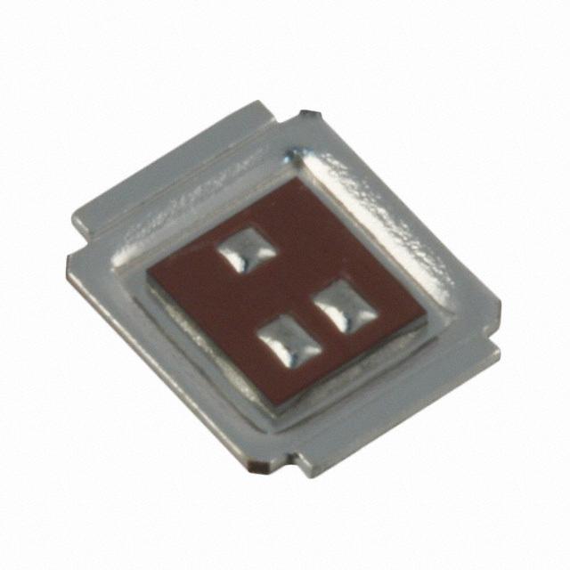
ICGOO电子元器件商城为您提供TPCA8026(TE12L,Q,M由Toshiba America Electronic Components, Inc.设计生产,在icgoo商城现货销售,并且可以通过原厂、代理商等渠道进行代购。 TPCA8026(TE12L,Q,M价格参考。Toshiba America Electronic Components, Inc.TPCA8026(TE12L,Q,M封装/规格:晶体管 - FET,MOSFET - 单, 表面贴装 N 沟道 30V 45A(Ta) 1.6W(Ta),45W(Tc) 8-SOP Advance(5x5)。您可以下载TPCA8026(TE12L,Q,M参考资料、Datasheet数据手册功能说明书,资料中有TPCA8026(TE12L,Q,M 详细功能的应用电路图电压和使用方法及教程。
| 参数 | 数值 |
| 产品目录 | |
| 描述 | MOSFET N-CH 30V 45A 8-SOP ADV |
| 产品分类 | FET - 单 |
| FET功能 | 逻辑电平门 |
| FET类型 | MOSFET N 通道,金属氧化物 |
| 品牌 | Toshiba Semiconductor and Storage |
| 数据手册 | http://www.semicon.toshiba.co.jp/info/docget.jsp?pid=TPCA8026&lang=en&type=datasheet点击此处下载产品Datasheet |
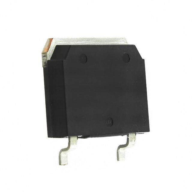
| 产品图片 |
|
| 产品型号 | TPCA8026(TE12L,Q,M |
| rohs | 无铅 / 符合限制有害物质指令(RoHS)规范要求 |
| 产品系列 | - |
| 不同Id时的Vgs(th)(最大值) | 2.5V @ 1mA |
| 不同Vds时的输入电容(Ciss) | 4200pF @ 10V |
| 不同Vgs时的栅极电荷(Qg) | 113nC @ 10V |
| 不同 Id、Vgs时的 RdsOn(最大值) | 2.2 毫欧 @ 23A,10V |
| 产品目录绘图 |
|
| 产品目录页面 | |
| 供应商器件封装 | 8-SOP 高级 |
| 其它名称 | TPCA8026TE12LQMTR |
| 功率-最大值 | 45W |
| 包装 | 带卷 (TR) |
| 安装类型 | 表面贴装 |
| 封装/外壳 | 8-PowerVDFN |
| 标准包装 | 3,000 |
| 漏源极电压(Vdss) | 30V |
| 电流-连续漏极(Id)(25°C时) | 45A (Ta) |


- 商务部:美国ITC正式对集成电路等产品启动337调查
- 曝三星4nm工艺存在良率问题 高通将骁龙8 Gen1或转产台积电
- 太阳诱电将投资9.5亿元在常州建新厂生产MLCC 预计2023年完工
- 英特尔发布欧洲新工厂建设计划 深化IDM 2.0 战略
- 台积电先进制程称霸业界 有大客户加持明年业绩稳了
- 达到5530亿美元!SIA预计今年全球半导体销售额将创下新高
- 英特尔拟将自动驾驶子公司Mobileye上市 估值或超500亿美元
- 三星加码芯片和SET,合并消费电子和移动部门,撤换高东真等 CEO
- 三星电子宣布重大人事变动 还合并消费电子和移动部门
- 海关总署:前11个月进口集成电路产品价值2.52万亿元 增长14.8%


PDF Datasheet 数据手册内容提取
TPCA8026 TOSHIBA Field Effect Transistor Silicon N-Channel MOS Type (U-MOSⅣ) TPCA8026 Lithium-Ion Battery Applications Unit: mm Notebook PC Applications 1.27 0.4 ± 0.1 Portable Equipment Applications 8 0.05 MA 5 0.3 0.2 • Small footprint due to a small and thin package 0 ± 0 ± 0.15 ± 0.05 6. 5. • Low drain-source ON-resistance: RDS (ON) = 1.8 mΩ (typ.) • High forward transfer admittance: |Yfs| =100 S (typ.) 1 4 0.595 • • ELonwh alneacekmageen tc umrroednet: :V ItDhS =S 1=. 31 0t oμ 2A. 5(m Va (xV) D(VS D=S 1 =0 3V0, IVD) = 1 mA) 0.95 0.05± 5.0 ± 0.2 0.166 0.05± A 0.05 S S 2 0. ± Absolute Maximum Ratings (Ta = 25°C) 1 4 1.1 1 0. Characteristic Symbol Rating Unit 0.6 ± 4.25 ± 0.2 0.2± 5 Drain-source voltage VDSS 30 V 3. Drain-gate voltage (RGS = 20 kΩ) VDGR 30 V 8 5 1 Gate-source voltage VGSS ±20 V 8 0.± 0. DC (Note 1) ID 45 Drain current A 1,2,3: SORCE 4: GATE Pulsed (Note 1) IDP 135 5,6,7,8:DRAIN Drain power dissipation (Tc = 25℃) PD 45 W JEDEC ⎯ Drain power dissipation (t = 10 s) JEITA ⎯ PD 2.8 W (Note 2a) TOSHIBA 2-5Q1A Drain power dissipation (t = 10 s) PD 1.6 W Weight: 0.069 g (typ.) (Note 2b) Single-pulse avalanche energy EAS 263 mJ (Note 3) Circuit Configuration Avalanche current IAR 45 A Repetitive avalanche energy (Tc = 25℃) (Note 4) EAR 3.4 mJ 8 7 6 5 Channel temperature Tch 150 °C Storage temperature range Tstg −55 to 150 °C Note: For Notes 1 to 4, refer to the next page. Using continuously under heavy loads (e.g. the application of high temperature/current/voltage and the significant change in 1 2 3 4 temperature, etc.) may cause this product to decrease in the reliability significantly even if the operating conditions (i.e. operating temperature/current/voltage, etc.) are within the absolute maximum ratings. Please design the appropriate reliability upon reviewing the Toshiba Semiconductor Reliability Handbook (“Handling Precautions”/“Derating Concept and Methods”) and individual reliability data (i.e. reliability test report and estimated failure rate, etc). This transistor is an electrostatic-sensitive device. Handle with care. 1 2008-06-26
TPCA8026 Thermal Characteristics Characteristic Symbol Max Unit Thermal resistance, channel to case Rth (ch-c) 2.78 °C/W (Tc = 25℃) Thermal resistance, channel to ambient Rth (ch-a) 44.6 °C/W (t = 10 s) (Note 2a) Thermal resistance, channel to ambient Rth (ch-a) 78.1 °C/W (t = 10 s) (Note 2b) Marking (Note 5) TPCA Part number 8026 ∗ Lot No. Note 1: Ensure that the channel temperature does not exceed 150°C. Note 2: (a) Device mounted on a glass-epoxy board (a) (b) Device mounted on a glass-epoxy board (b) FR-4 FR-4 25.4 × 25.4 × 0.8 25.4 × 25.4 × 0.8 (Unit: mm) (Unit: mm) (a) (b) Note 3: VDD = 24 V, Tch = 25°C (initial), L = 0.1 mH, IAR = 45 A Note 4: Repetitive rating: pulse width limited by maximum channel temperature Note 5: ∗ Weekly code: (Three digits) Week of manufacture (01 for the first week of the year, continuing up to 52 or 53) Year of manufacture (The last digit of the year) 2 2008-06-26
TPCA8026 Electrical Characteristics (Ta = 25°C) Characteristic Symbol Test Condition Min Typ. Max Unit Gate leakage current IGSS VGS = ±20 V, VDS = 0 V ⎯ ⎯ ±100 nA Drain cutoff current IDSS VDS = 30 V, VGS = 0 V ⎯ ⎯ 10 μA V (BR) DSS ID = 10 mA, VGS = 0 V 30 ⎯ ⎯ Drain-source breakdown voltage V V (BR) DSX ID = 10 mA, VGS = −20 V 10 ⎯ ⎯ Gate threshold voltage Vth VDS = 10 V, ID = 1 mA 1.3 ⎯ 2.5 V VGS = 4.5 V, ID = 23 A ⎯ 2.7 4.5 Drain-source ON-resistance RDS (ON) mΩ VGS = 10 V, ID = 23 A ⎯ 1.8 2.2 Forward transfer admittance |Yfs| VDS = 10 V, ID = 23 A 50 100 ⎯ S Input capacitance Ciss ⎯ 4200 ⎯ Reverse transfer capacitance Crss VDS = 10 V, VGS = 0 V, f = 1 MHz ⎯ 1000 ⎯ pF Output capacitance Coss ⎯ 1400 ⎯ Rise time tr ⎯ 15 ⎯ 10 V ID = 23A Turn-on time ton VGS 0 V ΩVOUT ⎯ 30 ⎯ 5 Switching time Ω 0.6 ns Fall time tf 4.7 =L ⎯ 36 ⎯ R VDD ≈ 15 V Turn-off time toff ⎯ 111 ⎯ Duty ≤ 1%, tw = 10 μs Total gate charge (gate-source plus gate-drain) Qg ⎯ 113 ⎯ Gate-source charge 1 Qgs1 VDD ≈ 24 V, VGS = 10 V, ID = 45 A ⎯ 13 ⎯ nC Gate-drain (“miller”) charge Qgd ⎯ 42 ⎯ Source-Drain Ratings and Characteristics (Ta = 25°C) Characteristic Symbol Test Condition Min Typ. Max Unit Drain reverse current Pulse (Note 1) IDRP ⎯ ⎯ ⎯ 135 A Forward voltage (diode) VDSF IDR = 45 A, VGS = 0 V ⎯ ⎯ −1.2 V 3 2008-06-26
TPCA8026 ID – VDS 108 ID – VDS 50 100 10 3.8 3.6 4 3.8 3.6 8 4 3.4 4.5 A) 40 4.5 A) 80 56 Common source ( 5 ( Ta = 25°C D 6 Common source D Pulse test I 30 Ta = 25°C I 60 current 20 Pulse test 3.2 current 40 3.4 ain ain 3.2 Dr 10 3 Dr 20 3 VGS = 2.8 V VGS = 2.8 V 0 0 0 0.2 0.4 0.6 0.8 1 0 1 2 3 4 5 Drain−source voltage VDS (V) Drain-source voltage VDS (V) ID – VGS VDS – VGS 100 0.4 Common source Common source VDS = 10 V V) Ta = 25°C Pulse test ( Pulse test 80 0.32 A) DS ( V I D 60 e 0.24 g ent olta curr 40 ce v 0.16 ain 100 Ta = −55°C our Dr s− ID = 45 A 20 n 0.08 25 Drai 23 12 0 0 0 1 2 3 4 5 6 0 2 4 6 8 10 Gate−source voltage VGS (V) Gate−source voltage VGS (V) |Yfs| – ID RDS (ON) – ID 1000 100 Common source Ta = 25°C mittance 100 Ta = −55°C sistance ) Ω Pulse test d transfer ad|Y| (S) fs 10 100 25 source ON-reR (mDS (ON) 10 Forwar 1 CVDomS m= o1n0 sVo urce Drain− 4.5 Pulse test VGS = 10 V 0.1 1 0.1 1 10 100 0.1 1 10 100 Drain current ID (A) Drain current ID (A) 4 2008-06-26
TPCA8026 RDS (ON) – Ta IDR – VDS 8 1000 Common source e Pulse test (A) anc 6 R 100 10 4.5 3 1 sist) Ω ID ource ON-re (mDS (ON) 4 VGS = 4.5 V ID = 12, 23, 45 A erse current 10 VGS = 0 V sR v ain- 2 ID = 12, 23, 45 A n re 1 Dr ai Common source VGS = 10 V Dr Ta = 25°C Pulse test 0 0.1 −80 −40 0 40 80 120 160 0 −0.2 −0.4 −0.6 −0.8 −1 Ambient temperature Ta (°C) Drain−source voltage VDS (V) Capacitance – VDS Vth – Ta 10000 3 Ciss (V) 2.5 pF) V th C ( 1000 Coss ge 2 ce Crss volta 1.5 citan hold a 100 s 1 p e Ca Common source e thr Common source VGS = 0 V at 0.5 VDS = 10 V f = 1 MHz G ID = 1mA Ta = 25°C Pulse test 10 0 0.1 1 10 100 −80 −40 0 40 80 120 160 Drain−source voltage VDS (V) Ambient temperature Ta (°C) Dynamic input/output characteristics 50 20 Common source V) ID = 40 A V) (S 40 TPau l=s e2 5te°sCt 16 (S D G V V Drainsource voltage − 312000 VDS VDDV =G 6SV 24 12 814 2 Gatesource voltage − 0 0 0 20 40 60 80 100 120 140 160 180 Total gate charge Qg (nC) 5 2008-06-26
TPCA8026 rth − tw 1000 (1) Device mounted on a glass-epoxy board (a) (Note 2a) (2) Device mounted on a glass-epoxy board (b) (Note 2b) e (3) Tc = 25℃ (2) c n a 100 ed (1) mpW) al iC/ m(° 10 her h (3) nt t rt e nsi 1 a Tr Single pulse 0.1 0.001 0.01 0.1 1 10 100 1000 Pulse width tw (s) PD – Ta PD – Tc 3 50 (1) Device mounted on a W) (1) glass-epoxy board (a) (Note 2a) W) ( 2.5 (2) Device mounted on a ( glass-epoxy board (b) (Note 2b) 40 P D t = 10 s P D n 2 n o o 30 ati (2) ati sip 1.5 sip s s di di 20 er 1 er w w o o p p n n 10 ai 0.5 ai Dr Dr 0 0 0 40 80 120 160 0 40 80 120 160 Ambient temperature Ta (°C) Case temperature Tc (°C) Safe operating area 1000 ID max (Pulse) * 1 ms * (A) 100 ID max (continuous) t = 10 ms * D I ent 10 DC operation urr Tc = 25 °C c n ai Dr 1 * Single pulse Ta = 25°C Curves must be derated linearly with increase in temperature. VDSS max 0.1 0.1 1 10 100 Drain−source voltage VDS (V) 6 2008-06-26
TPCA8026 RESTRICTIONS ON PRODUCT USE • Toshiba Corporation, and its subsidiaries and affiliates (collectively “TOSHIBA”), reserve the right to make changes to the information in this document, and related hardware, software and systems (collectively “Product”) without notice. • This document and any information herein may not be reproduced without prior written permission from TOSHIBA. Even with TOSHIBA’s written permission, reproduction is permissible only if reproduction is without alteration/omission. • Though TOSHIBA works continually to improve Product’s quality and reliability, Product can malfunction or fail. Customers are responsible for complying with safety standards and for providing adequate designs and safeguards for their hardware, software and systems which minimize risk and avoid situations in which a malfunction or failure of Product could cause loss of human life, bodily injury or damage to property, including data loss or corruption. Before creating and producing designs and using, customers must also refer to and comply with (a) the latest versions of all relevant TOSHIBA information, including without limitation, this document, the specifications, the data sheets and application notes for Product and the precautions and conditions set forth in the “TOSHIBA Semiconductor Reliability Handbook” and (b) the instructions for the application that Product will be used with or for. Customers are solely responsible for all aspects of their own product design or applications, including but not limited to (a) determining the appropriateness of the use of this Product in such design or applications; (b) evaluating and determining the applicability of any information contained in this document, or in charts, diagrams, programs, algorithms, sample application circuits, or any other referenced documents; and (c) validating all operating parameters for such designs and applications. TOSHIBA ASSUMES NO LIABILITY FOR CUSTOMERS’ PRODUCT DESIGN OR APPLICATIONS. • Product is intended for use in general electronics applications (e.g., computers, personal equipment, office equipment, measuring equipment, industrial robots and home electronics appliances) or for specific applications as expressly stated in this document. Product is neither intended nor warranted for use in equipment or systems that require extraordinarily high levels of quality and/or reliability and/or a malfunction or failure of which may cause loss of human life, bodily injury, serious property damage or serious public impact (“Unintended Use”). Unintended Use includes, without limitation, equipment used in nuclear facilities, equipment used in the aerospace industry, medical equipment, equipment used for automobiles, trains, ships and other transportation, traffic signaling equipment, equipment used to control combustions or explosions, safety devices, elevators and escalators, devices related to electric power, and equipment used in finance-related fields. Do not use Product for Unintended Use unless specifically permitted in this document. • Do not disassemble, analyze, reverse-engineer, alter, modify, translate or copy Product, whether in whole or in part. • Product shall not be used for or incorporated into any products or systems whose manufacture, use, or sale is prohibited under any applicable laws or regulations. • The information contained herein is presented only as guidance for Product use. No responsibility is assumed by TOSHIBA for any infringement of patents or any other intellectual property rights of third parties that may result from the use of Product. No license to any intellectual property right is granted by this document, whether express or implied, by estoppel or otherwise. • ABSENT A WRITTEN SIGNED AGREEMENT, EXCEPT AS PROVIDED IN THE RELEVANT TERMS AND CONDITIONS OF SALE FOR PRODUCT, AND TO THE MAXIMUM EXTENT ALLOWABLE BY LAW, TOSHIBA (1) ASSUMES NO LIABILITY WHATSOEVER, INCLUDING WITHOUT LIMITATION, INDIRECT, CONSEQUENTIAL, SPECIAL, OR INCIDENTAL DAMAGES OR LOSS, INCLUDING WITHOUT LIMITATION, LOSS OF PROFITS, LOSS OF OPPORTUNITIES, BUSINESS INTERRUPTION AND LOSS OF DATA, AND (2) DISCLAIMS ANY AND ALL EXPRESS OR IMPLIED WARRANTIES AND CONDITIONS RELATED TO SALE, USE OF PRODUCT, OR INFORMATION, INCLUDING WARRANTIES OR CONDITIONS OF MERCHANTABILITY, FITNESS FOR A PARTICULAR PURPOSE, ACCURACY OF INFORMATION, OR NONINFRINGEMENT. • Do not use or otherwise make available Product or related software or technology for any military purposes, including without limitation, for the design, development, use, stockpiling or manufacturing of nuclear, chemical, or biological weapons or missile technology products (mass destruction weapons). Product and related software and technology may be controlled under the Japanese Foreign Exchange and Foreign Trade Law and the U.S. Export Administration Regulations. Export and re-export of Product or related software or technology are strictly prohibited except in compliance with all applicable export laws and regulations. • Please contact your TOSHIBA sales representative for details as to environmental matters such as the RoHS compatibility of Product. Please use Product in compliance with all applicable laws and regulations that regulate the inclusion or use of controlled substances, including without limitation, the EU RoHS Directive. TOSHIBA assumes no liability for damages or losses occurring as a result of noncompliance with applicable laws and regulations. 7 2008-06-26