ICGOO在线商城 > TPA2039D1YFFT
 Datasheet下载
- 型号: TPA2039D1YFFT
- 制造商: Texas Instruments
- 库位|库存: xxxx|xxxx
- 要求:
| 数量阶梯 | 香港交货 | 国内含税 |
| +xxxx | $xxxx | ¥xxxx |
查看当月历史价格
查看今年历史价格
TPA2039D1YFFT产品简介:
ICGOO电子元器件商城为您提供TPA2039D1YFFT由Texas Instruments设计生产,在icgoo商城现货销售,并且可以通过原厂、代理商等渠道进行代购。 提供TPA2039D1YFFT价格参考以及Texas InstrumentsTPA2039D1YFFT封装/规格参数等产品信息。 你可以下载TPA2039D1YFFT参考资料、Datasheet数据手册功能说明书, 资料中有TPA2039D1YFFT详细功能的应用电路图电压和使用方法及教程。
| 参数 | 数值 |
| 产品目录 | 集成电路 (IC)半导体 |
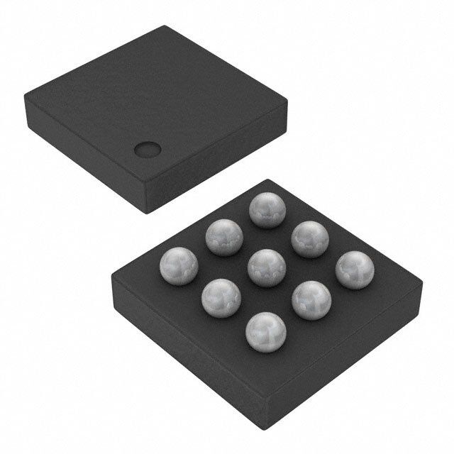
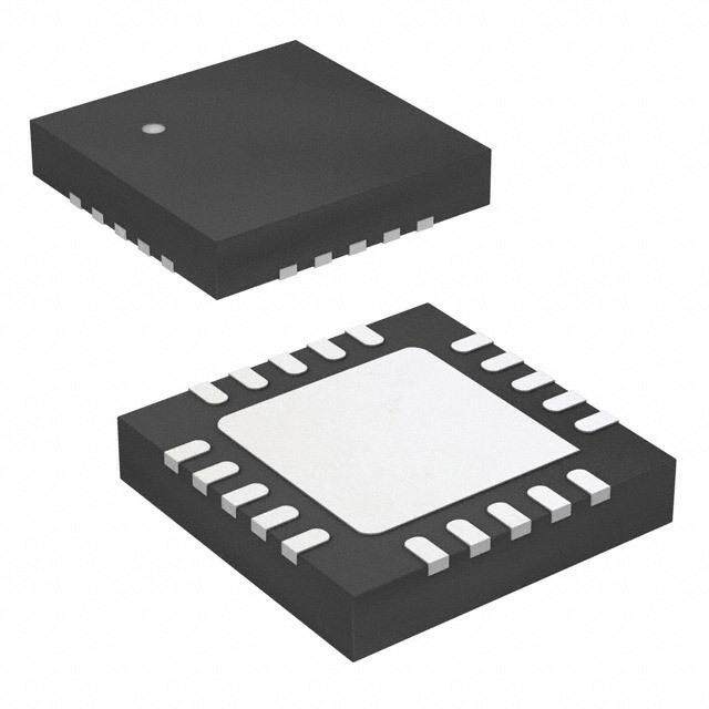
| 描述 | IC AMP AUD 3.2W MONO D 9DSBGA音频放大器 Fixed Gain 3.2W Mono Class-D |
| DevelopmentKit | TPA2039D1YFFEVM |
| 产品分类 | |
| 品牌 | Texas Instruments |
| 产品手册 | http://www.ti.com/litv/slos652a |
| 产品图片 |
|
| rohs | 符合RoHS无铅 / 符合限制有害物质指令(RoHS)规范要求 |
| 产品系列 | 音频 IC,音频放大器,Texas Instruments TPA2039D1YFFT- |
| 数据手册 | |
| 产品型号 | TPA2039D1YFFT |
| THD+噪声 | 0.12 % |
| 不同负载时的最大输出功率x通道数 | 3.24W x 1 @ 4 欧姆 |
| 产品 | Class-D |
| 产品种类 | 音频放大器 |
| 供应商器件封装 | 9-DSBGA(1.2x1.3) |
| 共模抑制比—最小值 | 77 dB |
| 其它名称 | 296-32457-1 |
| 包装 | 剪切带 (CT) |
| 商标 | Texas Instruments |
| 安装类型 | 表面贴装 |
| 安装风格 | SMD/SMT |
| 封装 | Reel |
| 封装/外壳 | 9-UFBGA,DSBGA |
| 封装/箱体 | DSBGA-9 |
| 工作温度 | -40°C ~ 85°C (TA) |
| 工作电源电压 | 2.5 V to 5.5 V |
| 工厂包装数量 | 250 |
| 最大功率耗散 | 525 mW |
| 最大工作温度 | + 85 C |
| 最小工作温度 | - 40 C |
| 标准包装 | 1 |
| 特性 | 差分输入,短路保护和热保护,关机 |
| 电压-电源 | 2.5 V ~ 5.5 V |
| 电源电压-最大 | 5.5 V |
| 电源电压-最小 | 2.5 V |
| 电源电流 | 1.5 mA |
| 类型 | D 类 |
| 系列 | TPA2039D1 |
| 输出功率 | 3.2 W |
| 输出类型 | 1-通道(单声道) |
| 通道数量 | 1 Channel |


- 商务部:美国ITC正式对集成电路等产品启动337调查
- 曝三星4nm工艺存在良率问题 高通将骁龙8 Gen1或转产台积电
- 太阳诱电将投资9.5亿元在常州建新厂生产MLCC 预计2023年完工
- 英特尔发布欧洲新工厂建设计划 深化IDM 2.0 战略
- 台积电先进制程称霸业界 有大客户加持明年业绩稳了
- 达到5530亿美元!SIA预计今年全球半导体销售额将创下新高
- 英特尔拟将自动驾驶子公司Mobileye上市 估值或超500亿美元
- 三星加码芯片和SET,合并消费电子和移动部门,撤换高东真等 CEO
- 三星电子宣布重大人事变动 还合并消费电子和移动部门
- 海关总署:前11个月进口集成电路产品价值2.52万亿元 增长14.8%


PDF Datasheet 数据手册内容提取
TPA2039D1 www.ti.com SLOS652A–DECEMBER2009–REVISEDJUNE2010 3.2W Mono Class-D Audio Power Amplifier With 12-dB Gain and Auto Short-Circuit Recovery CheckforSamples:TPA2039D1 FEATURES APPLICATIONS 1 • PowerfulMonoClass-DSpeakerAmplifier • WirelessorCellularHandsetsandPDAs – 3.24W(4 Ω,5V,10%THDN) • PortableNavigationDevices – 2.57W(4 Ω,5V,1%THDN) • GeneralPortableAudioDevices – 1.80W(8 Ω,5V,10%THDN) DESCRIPTION – 1.46W(8 Ω,5V,1%THDN) The TPA2039D1 is a 3.2 W high efficiency filter-free • +12dBFixedGain class-D audio power amplifier (class-D amp) with • IntegratedImageRejectFilterforDACNoise 12 dB of fixed gain in a tiny 1.21 mm x 1.16 mm Reduction wafer chip scale package (WCSP). The device • LowOutputNoiseof27mV requiresonlyoneexternalcomponent. • LowQuiescentCurrentof1.5mA Features like 93% efficiency, 1.5 mA quiescent • DifferentialInputImpedanceof150kΩ current, 0.1 mA shutdown current, 82-dB PSRR, 27mV output noise and improved RF immunity make • Auto-RecoveringShort-CircuitProtection the TPA2039D1 class-D amplifier ideal for cellular • Thermal-OverloadProtection handsets. A fast start-up time of 4ms with no audible • Filter-FreeMonoClass-DAmp pop makes the TPA2039D1 ideal for PDA and smart-phoneapplications. • 9-Ball1,21mm× 1,16mm0,4mmPitchWCSP APPLICATION CIRCUIT To battery TPA2039D1 VDD 9-BALL0.4mm PITCH Internal Cs WAFER CHIPSCALE PACKAGE(YFF) Oscillator (TOPVIEW OF PCB) IN+ VO- IN+ GND VO- + – PWM H-Bridge VO+ A1 A2 A3 IN- VDD PVDD PGND m EN CiBrciausitry GND B1 B2 B3 0m 6 1 1. TPA2039D1 IN- EN V + O C1 C2 C3 1.214mm 1 Pleasebeawarethatanimportantnoticeconcerningavailability,standardwarranty,anduseincriticalapplicationsofTexas Instrumentssemiconductorproductsanddisclaimerstheretoappearsattheendofthisdatasheet. PRODUCTIONDATAinformationiscurrentasofpublicationdate. Copyright©2009–2010,TexasInstrumentsIncorporated Products conform to specifications per the terms of the Texas Instruments standard warranty. Production processing does not necessarilyincludetestingofallparameters.
TPA2039D1 SLOS652A–DECEMBER2009–REVISEDJUNE2010 www.ti.com Thesedeviceshavelimitedbuilt-inESDprotection.Theleadsshouldbeshortedtogetherorthedeviceplacedinconductivefoam duringstorageorhandlingtopreventelectrostaticdamagetotheMOSgates. ORDERINGINFORMATION T PACKAGEDDEVICES(1) PARTNUMBER(2) SYMBOL A TPA2039D1YFFR DAR —40°Cto85°C 9-ballWSCP TPA2039D1YFFT DAR (1) Forthemostcurrentpackageandorderinginformation,seethePackageOptionAddendumattheendofthisdocument,orseetheTI Websiteatwww.ti.com (2) TheYFFpackageisonlyavailabletapedandreeled.Thesuffix"R"indicatesareelof3000,thesuffix"T"indicatesareelof250. ABSOLUTE MAXIMUM RATINGS overoperatingfree-airtemperaturerange,T =25°C(unlessotherwisenoted)(1) A VALUE UNIT Inactivemode –0.3to6.0 V V ,PV Supplyvoltage DD DD Inshutdownmode –0.3to6.0 V V Inputvoltage EN,IN+,IN– –0.3toV +0.3 V I DD R Minimumloadresistance 3.2 Ω L Outputcontinuoustotalpowerdissipation SeeDissipationRatingTable T Operatingfree-airtemperaturerange –40to85 °C A T Operatingjunctiontemperaturerange –40to150 °C J T Storagetemperaturerange –65to85 °C stg (1) Stressesbeyondthoselistedunderabsolutemaximumratingsmaycausepermanentdamagetothedevice.Thesearestressratings only,andfunctionaloperationofthedeviceattheseoranyotherconditionsbeyondthoseindicatedunderrecommendedoperating conditionsisnotimplied.ExposuretoAbsoluteMaximumRatingsconditionsforextendedperiodsmayaffectdevicereliability. DISSIPATION RATINGS PACKAGE DERATINGFACTOR(1) T <25°C T =70°C T =85°C A A A YFF(WCSP) 4.2mW/°C 525mW 336mW 273mW (1) DeratingfactormeasurewithhighKboard. RECOMMENDED OPERATING CONDITIONS MIN MAX UNIT V , Class-Dsupplyvoltage 2.5 5.5 V DD PV DD V High-levelinputvoltage EN 1.3 V IH V Low-levelinputvoltage EN 0.35 V IL V Commonmodeinputvoltagerange V =2.5V,5.5V,CMRR≥49dB 0.75 V -1.1 V IC DD DD T Operatingfree-airtemperature –40 85 °C A 2 SubmitDocumentationFeedback Copyright©2009–2010,TexasInstrumentsIncorporated ProductFolderLink(s):TPA2039D1
TPA2039D1 www.ti.com SLOS652A–DECEMBER2009–REVISEDJUNE2010 ELECTRICAL CHARACTERISTICS T =25°C(unlessotherwisenoted) A PARAMETER TESTCONDITIONS MIN TYP MAX UNIT Outputoffsetvoltage(measured |V | V =0V,V =2.5Vto5.5V 1 10 mV OS differentially) I DD |I | High-levelENinputcurrent V =5.5V,V =5.5V 50 mA IH DD EN |I | Low-levelENinputcurrent V =5.5V,V =0V 1 mA IL DD EN V =5.5V,noload 1.8 2.5 DD I Quiescentcurrent V =3.6V,noload 1.5 2.3 mA (Q) DD V =2.5V,noload 1.3 2.1 DD I Shutdowncurrent V =0.35V,V =3.6V 0.1 2 mA (SD) EN DD R Outputimpedanceinshutdownmode V =0.35V 2 kΩ O,SD EN f Switchingfrequency V =2.5Vto5.5V 250 300 350 kHz (SW) DD A Gain V =2.5Vto5.5V,R =noload 11.5 12 12.5 dB V DD L R ResistancefromENtoGND 300 kΩ EN R Singleendedinputresistance V ≥V 75 IN EN IH kΩ V ≤V 75 EN IL OPERATING CHARACTERISTICS V =3.6V,T =25°C,R =8Ω(unlessotherwisenoted) DD A L PARAMETER TESTCONDITIONS MIN TYP MAX UNIT V =5V 3.24 DD THD+N=10%,f=1kHz,R =4Ω V =3.6V 1.62 W L DD V =2.5V 0.70 DD V =5V 2.57 DD THD+N=1%,f=1kHz,R =4Ω V =3.6V 1.32 W L DD V =2.5V 0.57 DD P Outputpower O V =5V 1.80 DD THD+N=10%,f=1kHz,R =8Ω V =3.6V 0.91 W L DD V =2.5V 0.42 DD V =5V 1.46 DD THD+N=1%,f=1kHz,R =8Ω V =3.6V 0.74 W L DD V =2.5V 0.33 DD V =3.6V,InputsACgrounded A-weighting 27 DD V Noiseoutputvoltage mV n withCI=2mF,f=20Hzto20kHz Noweighting 36 RMS V =5.0V,P =1.0W,f=1kHz,R =8Ω 0.12% DD O L V =3.6V,P =0.5W,f=1kHz,R =8Ω 0.05% DD O L Totalharmonicdistortionplus VDD=2.5V,PO=0.2W,f=1kHz,RL=8Ω 0.05% THD+N noise V =5.0V,P =2.0W,f=1kHz,R =4Ω 0.32% DD O L V =3.6V,P =1.0W,f=1kHz,R =4Ω 0.11% DD O L V =2.5V,P =0.4W,f=1kHz,R =4Ω 0.12% DD O L V =3.6V,InputsACgroundedwithC =2mF, PSRR ACpowersupplyrejectionratio DD I 82 dB 200mV ripple,f=217Hz pp CMRR Commonmoderejectionratio V =3.6V,V =1V ,f=217Hz 77 dB DD IC PP T Startuptimefromshutdown V =3.6V 4 ms SU DD Copyright©2009–2010,TexasInstrumentsIncorporated SubmitDocumentationFeedback 3 ProductFolderLink(s):TPA2039D1
TPA2039D1 SLOS652A–DECEMBER2009–REVISEDJUNE2010 www.ti.com OPERATING CHARACTERISTICS (continued) V =3.6V,T =25°C,R =8Ω(unlessotherwisenoted) DD A L PARAMETER TESTCONDITIONS MIN TYP MAX UNIT V =3.6V,V shortedtoVDD 2 DD O+ V =3.6V,V shortedtoVDD 2 DD O– Shortcircuitprotection I V =3.6V,V shortedtoGND 2 A SC threshold DD O+ V =3.6V,V shortedtoGND 2 DD O– V =3.6V,V shortedtoV 2 DD O+ O– Timeforwhichoutputis disabledafterashortcircuit T event,afterwhich V =2.5Vto5.5V 100 ms AR DD auto-recoverytrialsare continuouslymade TerminalFunctions TERMINAL I/O DESCRIPTION NAME WCSPBALL IN– C1 I Negativedifferentialaudioinput. IN+ A1 I Positivedifferentialaudioinput. V A3 O NegativeBTLaudiooutput. O- V C3 O PositiveBTLaudiooutput. O+ Analoggroundterminal.MustbeconnectedtosamepotentialasPGNDusingadirectconnection GND A2 I toasinglepointground. High-currentAnaloggroundterminal.MustbeconnectedtosamepotentialasGNDusingadirect PGND B3 I connectiontoasinglepointground. Powersupplyterminal.MustbeconnectedtosamepowersupplyasPV usingadirect V B1 I DD DD connection.VoltagemustbewithinvalueslistedinRecommendedOperatingConditionstable. High-currentPowersupplyterminal.MustbeconnectedtosamepowersupplyasV usinga DD PV B2 I directconnection.VoltagemustbewithinvalueslistedinRecommendedOperatingConditions DD table. EN C2 I Enableterminal.ConnecttoLogicHighvoltagetoenabledevice,LogicLowvoltagetodisable (shutdown). FUNCTIONAL BLOCK DIAGRAM Input EN Buffer SC 300 KΩ 4 SubmitDocumentationFeedback Copyright©2009–2010,TexasInstrumentsIncorporated ProductFolderLink(s):TPA2039D1
TPA2039D1 www.ti.com SLOS652A–DECEMBER2009–REVISEDJUNE2010 TEST SETUP FOR GRAPHS CI + IN+ OUT+ + 30kHz MeaOsuutrpeumtent CI TPA2039D1 Load LoFwil tPearss MeasInupruemtent - IN- OUT- - VDD GND CS1 CS2 + VDD - 1. C was shorted for any common-mode input voltage measurement. All other measurements were taken with C = 0.1-mF I I (unlessotherwisenoted). 2. C =0.1mFisplacedveryclosetothedevice.TheoptionalC =10mFisusedfordatasheetgraphs. S1 S2 3. The 30-kHz low-pass filter is required even if the analyzer has an internal low-pass filter. An RC low-pass filter (1kΩ, 4700pF)isusedoneachoutputforthedatasheetgraphs. Copyright©2009–2010,TexasInstrumentsIncorporated SubmitDocumentationFeedback 5 ProductFolderLink(s):TPA2039D1
TPA2039D1 SLOS652A–DECEMBER2009–REVISEDJUNE2010 www.ti.com TYPICAL CHARACTERISTICS V =3.6V,C =0.1mF,C =0.1mF,C =10mF,T =25°C,R =8Ω(unlessotherwisenoted) DD I S1 S2 A L EFFICIENCY EFFICIENCY vsOUTPUTPOWER vsOUTPUTPOWER 100 100 90 90 80 80 70 70 % % ncy − 60 ncy − 60 e 50 e 50 Effici 40 Effici 40 − − h 30 RL = 8 W + 33 m H h 30 RL = 4 W + 33 m H 20 20 VDD = 2.5 V VDD = 2.5 V 10 VDD = 3.6 V 10 VDD = 3.6 V VDD = 5.0 V VDD = 5.0 V 0 0 0.0 0.2 0.4 0.6 0.8 1.0 1.2 1.4 1.6 1.8 2.0 0.0 0.4 0.8 1.2 1.6 2.0 2.4 2.8 3.2 3.6 4.0 PO − Output Power − W PO − Output Power − W Figure1. Figure2. POWERDISSIPATION POWERDISSIPATION vsOUTPUTPOWER vsOUTPUTPOWER 0.5 0.5 RL = 8 W + 33 m H VDD = 3.6 V RL = 8 W + 33 m H VDD = 5.0 V RL = 4 W + 33 m H RL = 4 W + 33 m H 0.4 0.4 W W − − n n o o ati 0.3 ati 0.3 p p Dissi Dissi wer 0.2 wer 0.2 o o P P − − P D P D 0.1 0.1 0.0 0.0 0.0 0.2 0.4 0.6 0.8 1.0 1.2 1.4 1.6 1.8 2.0 0.0 0.4 0.8 1.2 1.6 2.0 2.4 2.8 3.2 3.6 4.0 PO − Output Power − W PO − Output Power − W Figure3. Figure4. SUPPLYCURRENT SUPPLYCURRENT vsOUTPUTPOWER vsOUTPUTPOWER 900m 500m VDD = 2.5 V RL = 4 W + 33 m H VDD = 2.5 V RL = 8 W + 33 m H 800m VDD = 3.6 V VDD = 3.6 V 700m VDD = 5.0 V 400m VDD = 5.0 V A A nt − 600m nt − urre 500m urre 300m C C ply 400m ply up up 200m S S − 300m − I DD200m I DD100m 100m 0 0 0.0 0.4 0.8 1.2 1.6 2.0 2.4 2.8 3.2 3.6 4.0 0.0 0.2 0.4 0.6 0.8 1.0 1.2 1.4 1.6 1.8 2.0 PO − Output Power − W PO − Output Power − W Figure5. Figure6. 6 SubmitDocumentationFeedback Copyright©2009–2010,TexasInstrumentsIncorporated ProductFolderLink(s):TPA2039D1
TPA2039D1 www.ti.com SLOS652A–DECEMBER2009–REVISEDJUNE2010 TYPICAL CHARACTERISTICS (continued) V =3.6V,C =0.1mF,C =0.1mF,C =10mF,T =25°C,R =8Ω(unlessotherwisenoted) DD I S1 S2 A L SUPPLYCURRENT SUPPLYCURRENT vsSUPPLYVOLTAGE vsENVOLTAGE 2.00 200 RL = No Load VDD = 2.5 V RL = 8 W + 33 m H VDD = 3.6 V RL = 4 W + 33 m H VDD = 5.0 V A 1.75 A 150 m n Supply Current − 1.50 Supply Current − 100 I − DD 1.25 I − DD 50 1.00 0 2.5 3.0 3.5 4.0 4.5 5.0 5.5 0.0 0.1 0.2 0.3 0.4 0.5 VDD − Supply Voltage − V VEN − EN Voltage − V Figure7. Figure8. OUTPUTPOWER OUTPUTPOWER vsLOADRESISTANCE vsLOADRESISTANCE 4 4 THD+N = 10 % VDD = 2.5 V THD+N = 1 % VDD = 2.5 V Frequency = 1 kHz VDD = 3.6 V Frequency = 1 kHz VDD = 3.6 V VDD = 5.0 V VDD = 5.0 V W 3 W 3 − − er er w w o o P P ut 2 ut 2 p p ut ut O O − − O O P 1 P 1 0 0 4 8 12 16 20 24 28 32 4 8 12 16 20 24 28 32 RL − Load Resistance − W RL − Load Resistance − W Figure9. Figure10. OUTPUTPOWER THD+NOISE vsSUPPLYVOLTAGE vsOUTPUTPOWER 4 RL = 4 W , THD+N = 1 % − % 100 VDD = 2.5 V RL = 4 W + 33 m H W 3 RRRLLL === 488 WWW ,,, TTTHHHDDD+++NNN === 1110 0% %% n + Noise 10 VVDDDD == 35..60 VV ut Power − 2 nic Distortio 1 p o ut m − O Har P O 1 otal 0.1 T − N + Frequency = 1 kHz HD 0 T 0.01 2.5 3.0 3.5 4.0 4.5 5.0 10m 100m 1 5 VDD − Supply Voltage − V PO − Output Power − W Figure11. Figure12. Copyright©2009–2010,TexasInstrumentsIncorporated SubmitDocumentationFeedback 7 ProductFolderLink(s):TPA2039D1
TPA2039D1 SLOS652A–DECEMBER2009–REVISEDJUNE2010 www.ti.com TYPICAL CHARACTERISTICS (continued) V =3.6V,C =0.1mF,C =0.1mF,C =10mF,T =25°C,R =8Ω(unlessotherwisenoted) DD I S1 S2 A L THD+NOISE THD+NOISE vsOUTPUTPOWER vsFREQUENCY Noise − % 100 VVVDDDDDD === 235...560 VVV RL = 8 W + 33 m H Noise − % 10 VRDL D= = 8 5 W.0 + V 33 m H PPPOOO === 52105 W 0m mWW n + 10 n + 1 o o orti orti Dist Dist nic 1 nic 0.1 o o m m ar ar H H al al ot 0.1 ot 0.01 T T − − N N + + D D H H T 0.01 T 0.001 10m 100m 1 3 20 100 1k 10k 20k PO − Output Power − W f − Frequency − Hz Figure13. Figure14. THD+NOISE THD+NOISE vsFREQUENCY vsFREQUENCY % 10 % 10 Noise − VRDL D= = 8 3 W.6 + V 33 m H PPPOOO === 215520 50m mmWWW Noise − VRDL D= = 8 2 W.5 + V 33 m H PPPOOO === 172550 0mm mWWW n + 1 n + 1 o o orti orti Dist Dist nic 0.1 nic 0.1 o o m m ar ar H H al al ot 0.01 ot 0.01 T T − − N N + + D D H H T 0.001 T 0.001 20 100 1k 10k 20k 20 100 1k 10k 20k f − Frequency − Hz f − Frequency − Hz Figure15. Figure16. THD+NOISE THD+NOISE vsFREQUENCY vsFREQUENCY % 10 % 10 Noise − VRDL D= = 4 5 W.0 + V 33 m H PPPOOO === 15200 W00 mmWW Noise − VRDL D= = 4 3 W.6 + V 33 m H PPPOOO === 52105 W 0m mWW n + 1 n + 1 o o orti orti Dist Dist nic 0.1 nic 0.1 o o m m ar ar H H al al ot 0.01 ot 0.01 T T − − N N + + D D H H T 0.001 T 0.001 20 100 1k 10k 20k 20 100 1k 10k 20k f − Frequency − Hz f − Frequency − Hz Figure17. Figure18. 8 SubmitDocumentationFeedback Copyright©2009–2010,TexasInstrumentsIncorporated ProductFolderLink(s):TPA2039D1
TPA2039D1 www.ti.com SLOS652A–DECEMBER2009–REVISEDJUNE2010 TYPICAL CHARACTERISTICS (continued) V =3.6V,C =0.1mF,C =0.1mF,C =10mF,T =25°C,R =8Ω(unlessotherwisenoted) DD I S1 S2 A L THD+NOISE THD+NOISEvs vsFREQUENCY COMMONMODEINPUTVOLTAGE Noise − % 10 VRDL D= = 4 2 W.5 + V 33 m H PPPOOO === 314050 00m mmWWW Noise − % 10 RFPrOLe ==q u82e 0Wn0c +ym =3W3 1 m kHHz VVVDDDDDD === 235...560 VVV n + 1 n + ortio ortio 1 Dist Dist nic 0.1 nic o o m m ar ar H H 0.1 al al ot 0.01 ot T T − − N N + + D D H H T 0.001 T 0.01 20 100 1k 10k 20k 0.0 0.5 1.0 1.5 2.0 2.5 3.0 3.5 4.0 4.5 5.0 f − Frequency − Hz VIC − Common Mode Input Voltage − V Figure19. Figure20. POWERSUPPLYREJECTIONRATIO POWERSUPPLYREJECTIONRATIO vsFREQUENCY vsFREQUENCY 0 0 B Inputs AC−Grounded VDD = 2.5 V B Inputs AC−Grounded VDD = 2.5 V atio − d −−2100 CRIL == 28 mWF + 33 m H VVDDDD == 35..60 VV atio − d −−2100 CRIL == 24 mWF + 33 m H VVDDDD == 35..60 VV R R n −30 n −30 o o ejecti −40 ejecti −40 R R ply −50 ply −50 p p Su −60 Su −60 er er w −70 w −70 o o P P − −80 − −80 R R SR −90 SR −90 P P −100 −100 20 100 1k 10k 20k 20 100 1k 10k 20k f − Frequency − Hz f − Frequency − Hz Figure21. Figure22. POWERSUPPLYREJECTIONRATIO COMMONMODEREJECTIONRATIO vsCOMMONMODEINPUTVOLTAGE vsFREQUENCY 0 −30 ply Rejection Ratio − dB −−−−−5432100000 RFrLe =q u8e Wnc +y =33 2 m17H Hz VVVDDDDDD === 235...560 VVV ode Rejection Ratio − dB −−−654000 VRILC == 81 WV P+P 33 m H VVVDDDDDD === 235...560 VVV Sup −60 n M −70 er mo PSRR − Pow −−−987000 CMRR − Com −−9800 −100 −100 0.0 0.5 1.0 1.5 2.0 2.5 3.0 3.5 4.0 4.5 5.0 20 100 1k 10k 20k VIC − Common Mode Input Voltage − V f − Frequency − Hz Figure23. Figure24. Copyright©2009–2010,TexasInstrumentsIncorporated SubmitDocumentationFeedback 9 ProductFolderLink(s):TPA2039D1
TPA2039D1 SLOS652A–DECEMBER2009–REVISEDJUNE2010 www.ti.com TYPICAL CHARACTERISTICS (continued) V =3.6V,C =0.1mF,C =0.1mF,C =10mF,T =25°C,R =8Ω(unlessotherwisenoted) DD I S1 S2 A L COMMONMODEREJECTIONRATIO vsCOMMONMODEINPUTVOLTAGE 0 dB RL = 8 W + 33 m H VDD = 2.5 V atio − −−2100 Frequency = 217 Hz VVDDDD == 35..60 VV R on −30 ecti ej −40 R de −50 o M n −60 o m m −70 o C − −80 R MR −90 C −100 0.0 0.5 1.0 1.5 2.0 2.5 3.0 3.5 4.0 4.5 5.0 VIC − Common Mode Input Voltage − V Figure25. GSMPOWERSUPPLYREJECTION vsTIME C1 - High VDD 3.6 V 500 mV/div C1 -Amplitude 500 mV C1 - Duty Cycle 20% V OUT 100mV/div 0 2.5 5 7.5 10 12.5 15 17.5 20 22.5 25 t−Time−ms Figure26. GSMPOWERSUPPLYREJECTION vsFREQUENCY 0 V B −25 −d −50 ge a −75 olt V −100 ply −125 up S V −25 −150 − B D −d −50 −175 VD ge −75 a olt −100 V ut −125 p ut −150 O − −175 O V −200 0 2.4 4.8 7.2 9.6 12 14.4 16.8 19.2 21.6 24 f−Frequency−kHz Figure27. 10 SubmitDocumentationFeedback Copyright©2009–2010,TexasInstrumentsIncorporated ProductFolderLink(s):TPA2039D1
TPA2039D1 www.ti.com SLOS652A–DECEMBER2009–REVISEDJUNE2010 APPLICATION INFORMATION SHORT CIRCUIT AUTO-RECOVERY When a short-circuit event occurs, the TPA2039D1 goes to shutdown mode and activates the integrated auto-recovery process whose aim is to return the device to normal operation once the short-circuit is removed. This process repeatedly examines (once every 100ms) whether the short-circuit condition persists, and returns the device to normal operation immediately after the short-circuit condition is removed. This feature helps protect thedevicefromlargecurrentsandmaintainagoodlong-termreliability. INTEGRATED IMAGE REJECT FILTER FOR DAC NOISE REJECTION In applications which use a DAC to drive Class-D amplifiers, out-of-band noise energy present at the DAC's image frequencies fold back into the audio-band at the output of the Class-D amplifier. An external low-pass filter isoftenplacedbetweentheDACandtheClass-Damplifierinordertoattenuatethisnoise. The TPA2039D1 has an integrated Image Reject Filter with a low-pass cutoff frequency of 130 kHz, which significantly attenuates this noise. Depending on the system noise specification, the integrated Image Reject Filtermayhelpeliminateexternalfiltering,therebysavingboardspaceandcomponentcost. COMPONENT SELECTION Figure 28 shows the TPA2039D1 typical schematic with differential inputs, while Figure 29 shows the TPA2039D1 with differential inputs and input capacitors. Figure 30 shows the TPA2039D1 with a single-ended input. DecouplingCapacitors(C ,C ) S1 S2 The TPA2039D1 is a high-performance class-D audio amplifier that requires adequate power supply decoupling to ensure the efficiency is high and total harmonic distortion (THD) is low. For higher frequency transients, spikes,ordigitalhashontheline,agoodlowequivalent-series-resistance(ESR)ceramiccapacitorC =0.1mF, S1 placed as close as possible to the device V lead works best. Placing C close to the TPA2039D1 is important DD S1 for the efficiency of the class-D amplifier, because any resistance or inductance in the trace between the device and the capacitor can cause a loss in efficiency. For filtering lower-frequency noise signals, a 10 mF or greater capacitor (C ) placed near the audio power amplifier would also help, but it is not required in most applications S2 because of the high PSRR of this device. Typically, the smaller the capacitor's case size, the lower the inductance and the closer it can be placed to the TPA2039D1. X5R and X7R dielectric capacitors are recommendedforbothC andC . S1 S2 InputCapacitors(C) I The TPA2039D1 does not require input coupling capacitors if the design uses a differential source that is biased within the common-mode input voltage range. That voltage range is listed in the Recommended Operating Conditions table. If the input signal is not biased within the recommended common-mode input range, such as in needing to use the input as a high pass filter, shown in Figure 29, or if using a single-ended source, shown in Figure 30, input coupling capacitors are required. The same value capacitors should be used on both IN+ and IN– for best pop performance. The 3-dB high-pass cutoff frequency f of the filter formed by the input coupling C capacitorC andtheinputresistanceR (typically75kΩ)oftheTPA2039D1isgivenbyEquation1: I I 1 f = C (2πRC ) I I (1) The value of the input capacitor is important to consider as it directly affects the bass (low frequency) performance of the circuit. Speaker response may also be taken into consideration when setting the corner frequencyusinginputcapacitors.Solvingfortheinputcouplingcapacitance,weget: 1 C = I (2πRf ) IC (2) If the corner frequency is within the audio band, the capacitors should have a tolerance of ±10% or better, becauseanymismatchincapacitancecausesanimpedancemismatchatthecornerfrequencyandbelow. Copyright©2009–2010,TexasInstrumentsIncorporated SubmitDocumentationFeedback 11 ProductFolderLink(s):TPA2039D1
TPA2039D1 SLOS652A–DECEMBER2009–REVISEDJUNE2010 www.ti.com For a flat low-frequency response, use large input coupling capacitors (0.1 mF or larger). X5R and X7R dielectric capacitorsarerecommended. To Battery Internal VDD Oscillator CS IN− VO− PWM H− _ Differential Bridge Input + VO+ IN+ Bias GND EN Circuitry TPA2039D1 Filter-Free Class D Figure28. TypicalTPA2039D1ApplicationSchematicWithDC-coupledDifferentialInput To Battery Internal VDD CI Oscillator CS IN− VO− _ PWM H− Differential Bridge Input CI + VO+ IN+ GND Bias EN Circuitry TPA2039D1 Filter-Free Class D Figure29. TPA2039D1ApplicationSchematicWithDifferentialInputandInputCapacitors To Battery Internal VDD CI Oscillator CS Single-ended IN− Input VO− PWM H− _ Bridge + VO+ IN+ CI GND Bias EN Circuitry TPA2039D1 Filter-Free Class D Figure30. TPA2039D1ApplicationSchematicWithSingle-EndedInput 12 SubmitDocumentationFeedback Copyright©2009–2010,TexasInstrumentsIncorporated ProductFolderLink(s):TPA2039D1
TPA2039D1 www.ti.com SLOS652A–DECEMBER2009–REVISEDJUNE2010 EFFICIENCY AND THERMAL INFORMATION The maximum ambient operating temperature of the TPA2039D1 depends on the load resistance, power supply voltage and heat-sinking ability of the PCB system. The derating factor for the YFF package is shown in the dissipationratingtable.Convertingthistoq : JA (cid:1) (cid:1) 1 JA DeratingFactor (3) Given q (from the Package Dissipation ratings table), the maximum allowable junction temperature (from the JA Absolute Maximum ratings table), and the maximum internal dissipation (from Power Dissipation vs Output Power figures) the maximum ambient temperature can be calculated with the following equation. Note that the units on these figures are Watts RMS. Because of crest factor (ratio of peak power to RMS power) from 9–15 dB,thermallimitationsarenotusuallyencountered. T Max(cid:2)T Max (cid:1) (cid:1) P A J JA Dmax (4) The TPA2039D1 is designed with thermal protection that turns the device off when the junction temperature surpasses 150°C to prevent damage to the IC. Note that the use of speakers less resistive than 4-Ω (typ) is not advisable. Below 4-Ω (typ) the thermal performance of the device dramatically reduces because of increased output current and reduced amplifier efficiency. The Absolute Maximum rating of 3.2-Ω covers the manufacturing tolerance of a 4-Ω speaker and speaker impedance decrease due to frequency. q is a gross approximation of JA the complex thermal transfer mechanisms between the device and its ambient environment. If the q calculation JA revealsapotentialproblem,amoreaccurateestimateshouldbemade. WHEN TO USE AN OUTPUT FILTER Design the TPA2039D1 without an Inductor / Capacitor (LC) output filter if the traces from the amplifier to the speaker are short. Wireless handsets and PDAs are great applications for this class-D amplifier to be used withoutanoutputfilter. The TPA2039D1 does not require an LC output filter for short speaker connections (approximately 100 mm long or less). A ferrite bead can often be used in the design if failing radiated emissions testing without an LC filter; and, the frequency-sensitive circuit is greater than 1 MHz. If choosing a ferrite bead, choose one with high impedance at high frequencies, but very low impedance at low frequencies. The selection must also take into account the currents flowing through the ferrite bead. Ferrites can begin to loose effectiveness at much lower thanratedcurrentvalues.SeetheTPA2039D1EVMUser'sGuideforcomponentsusedsuccessfullybyTI. Figure31showsatypicalferrite-beadoutputfilter. Ferrite Chip Bead VO− 1 nF Ferrite Chip Bead VO+ 1 nF Figure31. TypicalFerriteChipBeadFilter Copyright©2009–2010,TexasInstrumentsIncorporated SubmitDocumentationFeedback 13 ProductFolderLink(s):TPA2039D1
TPA2039D1 SLOS652A–DECEMBER2009–REVISEDJUNE2010 www.ti.com PRINTED CIRCUIT BOARD LAYOUT In making the pad size for the WCSP balls, it is recommended that the layout use nonsolder mask defined (NSMD) land. With this method, the solder mask opening is made larger than the desired land area, and the openingsizeisdefinedbythecopperpadwidth.Figure32showstheappropriatediametersforaWCSPlayout. Figure32. LandPatternImageandDimensions SDOELFDINEITRIOPNASD COPPERPAD SOOLPDEENRINMGA(5S)K THCIOCPKPNEERSS STENCILOPENING(6)(7) THSITCEKNNCEILSS Nonsoldermask 1ozmax 0.275mmx0.275mmSq. 0.23mm 0.310mm 0.1mmthick defined(NSMD) (0.032mm) (roundedcorners) 1. Circuit traces from NSMD defined PWB lands should be 75 mm to 100 mm wide in the exposed area inside thesoldermaskopening.Widertracewidthsreducedevicestandoffandimpactreliability. 2. Best reliability results are achieved when the PWB laminate glass transition temperature is above the operatingtherangeoftheintendedapplication. 3. RecommendsolderpasteisType3orType4. 4. For a PWB using a Ni/Au surface finish, the gold thickness should be less 0.5 mm to avoid a reduction in thermalfatigueperformance. 5. Soldermaskthicknessshouldbelessthan20mmontopofthecoppercircuitpattern 6. Best solder stencil performance is achieved using laser cut stencils with electro polishing. Use of chemically etchedstencilsgiveinferiorsolderpastevolumecontrol. 7. Trace routing away from WCSP device should be balanced in X and Y directions to avoid unintentional componentmovementduetosolderwettingforces. Figure33. LayoutSnapshot An on-pad via is not required to route the middle ball B2 (PV ) of the TPA2039D1. Just short ball B2 (PV ) to DD DD ball B1 (V ) and connect both to the supply trace as shown in Figure 33. This simplifies board routing and DD savesmanufacturingcost. 14 SubmitDocumentationFeedback Copyright©2009–2010,TexasInstrumentsIncorporated ProductFolderLink(s):TPA2039D1
TPA2039D1 www.ti.com SLOS652A–DECEMBER2009–REVISEDJUNE2010 Package Dimensions D E Max=1190µm Max=1244µm Min=1130µm Min=1184µm REVISION HISTORY ChangesfromOriginal(December2009)toRevisionA Page • ChangedthePackageDimensionstable.DwasMax=1244mm,Min=1184mm.EwasMax=1190mm,Min= 1130mm ............................................................................................................................................................................... 15 Copyright©2009–2010,TexasInstrumentsIncorporated SubmitDocumentationFeedback 15 ProductFolderLink(s):TPA2039D1
PACKAGE OPTION ADDENDUM www.ti.com 11-Apr-2013 PACKAGING INFORMATION Orderable Device Status Package Type Package Pins Package Eco Plan Lead/Ball Finish MSL Peak Temp Op Temp (°C) Top-Side Markings Samples (1) Drawing Qty (2) (3) (4) TPA2039D1YFFR ACTIVE DSBGA YFF 9 3000 Green (RoHS SNAGCU Level-1-260C-UNLIM -40 to 85 DAR & no Sb/Br) TPA2039D1YFFT ACTIVE DSBGA YFF 9 250 Green (RoHS SNAGCU Level-1-260C-UNLIM -40 to 85 DAR & no Sb/Br) (1) The marketing status values are defined as follows: ACTIVE: Product device recommended for new designs. LIFEBUY: TI has announced that the device will be discontinued, and a lifetime-buy period is in effect. NRND: Not recommended for new designs. Device is in production to support existing customers, but TI does not recommend using this part in a new design. PREVIEW: Device has been announced but is not in production. Samples may or may not be available. OBSOLETE: TI has discontinued the production of the device. (2) Eco Plan - The planned eco-friendly classification: Pb-Free (RoHS), Pb-Free (RoHS Exempt), or Green (RoHS & no Sb/Br) - please check http://www.ti.com/productcontent for the latest availability information and additional product content details. TBD: The Pb-Free/Green conversion plan has not been defined. Pb-Free (RoHS): TI's terms "Lead-Free" or "Pb-Free" mean semiconductor products that are compatible with the current RoHS requirements for all 6 substances, including the requirement that lead not exceed 0.1% by weight in homogeneous materials. Where designed to be soldered at high temperatures, TI Pb-Free products are suitable for use in specified lead-free processes. Pb-Free (RoHS Exempt): This component has a RoHS exemption for either 1) lead-based flip-chip solder bumps used between the die and package, or 2) lead-based die adhesive used between the die and leadframe. The component is otherwise considered Pb-Free (RoHS compatible) as defined above. Green (RoHS & no Sb/Br): TI defines "Green" to mean Pb-Free (RoHS compatible), and free of Bromine (Br) and Antimony (Sb) based flame retardants (Br or Sb do not exceed 0.1% by weight in homogeneous material) (3) MSL, Peak Temp. -- The Moisture Sensitivity Level rating according to the JEDEC industry standard classifications, and peak solder temperature. (4) Multiple Top-Side Markings will be inside parentheses. Only one Top-Side Marking contained in parentheses and separated by a "~" will appear on a device. If a line is indented then it is a continuation of the previous line and the two combined represent the entire Top-Side Marking for that device. Important Information and Disclaimer:The information provided on this page represents TI's knowledge and belief as of the date that it is provided. TI bases its knowledge and belief on information provided by third parties, and makes no representation or warranty as to the accuracy of such information. Efforts are underway to better integrate information from third parties. TI has taken and continues to take reasonable steps to provide representative and accurate information but may not have conducted destructive testing or chemical analysis on incoming materials and chemicals. TI and TI suppliers consider certain information to be proprietary, and thus CAS numbers and other limited information may not be available for release. In no event shall TI's liability arising out of such information exceed the total purchase price of the TI part(s) at issue in this document sold by TI to Customer on an annual basis. Addendum-Page 1
PACKAGE MATERIALS INFORMATION www.ti.com 22-Oct-2019 TAPE AND REEL INFORMATION *Alldimensionsarenominal Device Package Package Pins SPQ Reel Reel A0 B0 K0 P1 W Pin1 Type Drawing Diameter Width (mm) (mm) (mm) (mm) (mm) Quadrant (mm) W1(mm) TPA2039D1YFFR DSBGA YFF 9 3000 180.0 8.4 1.34 1.34 0.81 4.0 8.0 Q1 TPA2039D1YFFT DSBGA YFF 9 250 180.0 8.4 1.34 1.34 0.81 4.0 8.0 Q1 PackMaterials-Page1
PACKAGE MATERIALS INFORMATION www.ti.com 22-Oct-2019 *Alldimensionsarenominal Device PackageType PackageDrawing Pins SPQ Length(mm) Width(mm) Height(mm) TPA2039D1YFFR DSBGA YFF 9 3000 182.0 182.0 20.0 TPA2039D1YFFT DSBGA YFF 9 250 210.0 185.0 35.0 PackMaterials-Page2
PACKAGE OUTLINE YFF0009 DSBGA - 0.625 mm max height SCALE 10.000 DIE SIZE BALL GRID ARRAY B E A BALL A1 CORNER D 0.625 MAX C SEATING PLANE 0.30 0.12 BALL TYP 0.05 C 0.8 TYP C B SYMM 0.8 D: Max = 1.244 mm, Min =1 .184 mm TYP 0.4 TYP E: Max = 1.19 mm, Min = 1.13 mm A 9X 0.3 1 2 3 0.2 SYMM 0.015 C A B 0.4 TYP 4219552/A 05/2016 NOTES: 1. All linear dimensions are in millimeters. Any dimensions in parenthesis are for reference only. Dimensioning and tolerancing per ASME Y14.5M. 2. This drawing is subject to change without notice. www.ti.com
EXAMPLE BOARD LAYOUT YFF0009 DSBGA - 0.625 mm max height DIE SIZE BALL GRID ARRAY (0.4) TYP 9X ( 0.23) 1 2 3 A (0.4) TYP SYMM B C SYMM LAND PATTERN EXAMPLE SCALE:30X 0.05 MAX ( 0.23) 0.05 MIN METAL UNDER METAL SOLDER MASK SOLDER MASK ( 0.23) OPENING SOLDER MASK OPENING NON-SOLDER MASK SOLDER MASK DEFINED DEFINED (PREFERRED) SOLDER MASK DETAILS NOT TO SCALE 4219552/A 05/2016 NOTES: (continued) 3. Final dimensions may vary due to manufacturing tolerance considerations and also routing constraints. For more information, see Texas Instruments literature number SNVA009 (www.ti.com/lit/snva009). www.ti.com
EXAMPLE STENCIL DESIGN YFF0009 DSBGA - 0.625 mm max height DIE SIZE BALL GRID ARRAY (0.4) TYP (R0.05) TYP 9X ( 0.25) 1 2 3 A (0.4) TYP SYMM B METAL TYP C SYMM SOLDER PASTE EXAMPLE BASED ON 0.1 mm THICK STENCIL SCALE:30X 4219552/A 05/2016 NOTES: (continued) 4. Laser cutting apertures with trapezoidal walls and rounded corners may offer better paste release. www.ti.com
IMPORTANTNOTICEANDDISCLAIMER TIPROVIDESTECHNICALANDRELIABILITYDATA(INCLUDINGDATASHEETS),DESIGNRESOURCES(INCLUDINGREFERENCE DESIGNS),APPLICATIONOROTHERDESIGNADVICE,WEBTOOLS,SAFETYINFORMATION,ANDOTHERRESOURCES“ASIS” ANDWITHALLFAULTS,ANDDISCLAIMSALLWARRANTIES,EXPRESSANDIMPLIED,INCLUDINGWITHOUTLIMITATIONANY IMPLIEDWARRANTIESOFMERCHANTABILITY,FITNESSFORAPARTICULARPURPOSEORNON-INFRINGEMENTOFTHIRD PARTYINTELLECTUALPROPERTYRIGHTS. TheseresourcesareintendedforskilleddevelopersdesigningwithTIproducts.Youaresolelyresponsiblefor(1)selectingtheappropriate TIproductsforyourapplication,(2)designing,validatingandtestingyourapplication,and(3)ensuringyourapplicationmeetsapplicable standards,andanyothersafety,security,orotherrequirements.Theseresourcesaresubjecttochangewithoutnotice.TIgrantsyou permissiontousetheseresourcesonlyfordevelopmentofanapplicationthatusestheTIproductsdescribedintheresource.Other reproductionanddisplayoftheseresourcesisprohibited.NolicenseisgrantedtoanyotherTIintellectualpropertyrightortoanythird partyintellectualpropertyright.TIdisclaimsresponsibilityfor,andyouwillfullyindemnifyTIanditsrepresentativesagainst,anyclaims, damages,costs,losses,andliabilitiesarisingoutofyouruseoftheseresources. TI’sproductsareprovidedsubjecttoTI’sTermsofSale(www.ti.com/legal/termsofsale.html)orotherapplicabletermsavailableeitheron ti.comorprovidedinconjunctionwithsuchTIproducts.TI’sprovisionoftheseresourcesdoesnotexpandorotherwisealterTI’sapplicable warrantiesorwarrantydisclaimersforTIproducts. MailingAddress:TexasInstruments,PostOfficeBox655303,Dallas,Texas75265 Copyright©2019,TexasInstrumentsIncorporated