ICGOO在线商城 > 集成电路(IC) > 线性 - 音頻放大器 > TPA1517DWP
 Datasheet下载
- 型号: TPA1517DWP
- 制造商: Texas Instruments
- 库位|库存: xxxx|xxxx
- 要求:
| 数量阶梯 | 香港交货 | 国内含税 |
| +xxxx | $xxxx | ¥xxxx |
查看当月历史价格
查看今年历史价格
TPA1517DWP产品简介:
ICGOO电子元器件商城为您提供TPA1517DWP由Texas Instruments设计生产,在icgoo商城现货销售,并且可以通过原厂、代理商等渠道进行代购。 TPA1517DWP价格参考。Texas InstrumentsTPA1517DWP封装/规格:线性 - 音頻放大器, Amplifier IC 2-Channel (Stereo) Class AB 20-SO PowerPad。您可以下载TPA1517DWP参考资料、Datasheet数据手册功能说明书,资料中有TPA1517DWP 详细功能的应用电路图电压和使用方法及教程。
| 参数 | 数值 |
| 产品目录 | 集成电路 (IC)半导体 |
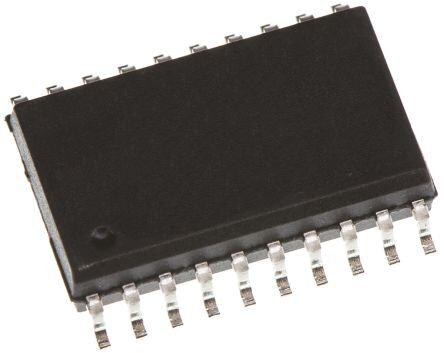
| 描述 | IC AMP AUDIO PWR 6W STER 20SOPWR音频放大器 6W Stereo Amp |
| DevelopmentKit | TPA1517DWPEVM |
| 产品分类 | |
| 品牌 | Texas Instruments |
| 产品手册 | http://www.ti.com/litv/slos162d |
| 产品图片 |
|
| rohs | 符合RoHS无铅 / 符合限制有害物质指令(RoHS)规范要求 |
| 产品系列 | 音频 IC,音频放大器,Texas Instruments TPA1517DWP- |
| 数据手册 | |
| 产品型号 | TPA1517DWP |
| THD+噪声 | 0.1 % |
| 不同负载时的最大输出功率x通道数 | 6W x 2 @ 4 欧姆 |
| 产品 | Class-D |
| 产品目录页面 | |
| 产品种类 | 音频放大器 |
| 供应商器件封装 | 20-SO PowerPad |
| 其它名称 | 296-7007-5 |
| 包装 | 管件 |
| 单位重量 | 506.600 mg |
| 商标 | Texas Instruments |
| 增益 | 20 dB |
| 安装类型 | 表面贴装 |
| 安装风格 | SMD/SMT |
| 封装 | Tube |
| 封装/外壳 | 20-SOIC(0.295",7.50mm 宽)裸露焊盘 |
| 封装/箱体 | HSOP-20 |
| 工作温度 | -40°C ~ 85°C (TA) |
| 工作电源电压 | 9.5 V to 18 V |
| 工厂包装数量 | 25 |
| 最大功率耗散 | 2940 mW |
| 最大工作温度 | + 85 C |
| 最小工作温度 | - 40 C |
| 标准包装 | 25 |
| 特性 | 静音,待机,热保护 |
| 电压-电源 | 9.5 V ~ 18 V |
| 电源电压-最大 | 18 V |
| 电源电压-最小 | 9.5 V |
| 电源电流 | 45 mA |
| 电源类型 | Single |
| 类型 | AB 类 |
| 系列 | TPA1517 |
| 输入信号类型 | Single |
| 输出信号类型 | Single |
| 输出功率 | 6 W |
| 输出类型 | 2 通道(立体声) |
| 配用 | /product-detail/zh/TPA1517NEEVM/296-10826-ND/381853/product-detail/zh/TPA1517DWPEVM/296-10825-ND/381770 |
| 音频负载电阻 | 8 Ohms |

.jpg)


- 商务部:美国ITC正式对集成电路等产品启动337调查
- 曝三星4nm工艺存在良率问题 高通将骁龙8 Gen1或转产台积电
- 太阳诱电将投资9.5亿元在常州建新厂生产MLCC 预计2023年完工
- 英特尔发布欧洲新工厂建设计划 深化IDM 2.0 战略
- 台积电先进制程称霸业界 有大客户加持明年业绩稳了
- 达到5530亿美元!SIA预计今年全球半导体销售额将创下新高
- 英特尔拟将自动驾驶子公司Mobileye上市 估值或超500亿美元
- 三星加码芯片和SET,合并消费电子和移动部门,撤换高东真等 CEO
- 三星电子宣布重大人事变动 还合并消费电子和移动部门
- 海关总署:前11个月进口集成电路产品价值2.52万亿元 增长14.8%


PDF Datasheet 数据手册内容提取
TPA1517 www.ti.com SLOS162D–MARCH1997–REVISEDFEBRUARY2007 6-W STEREO AUDIO POWER AMPLIFIER FEATURES • ThermalProtection • TDA1517PCompatible • FixedGain:20dB • HighPowerOutputs(6W/Channel) • MuteandStandbyOperation • SurfaceMountAvailability20-PinThermal • SupplyRange:9.5V-18V SOICPowerPAD™ NE PACKAGE DWP PACKAGE (TOP VIEW) (TOP VIEW) GND/HS 1 20 GND/HS IN1 1 20 GND/HS IN1 2 19 IN2 SGND 2 19 GND/HS NC 3 18 NC SVRR 3 18 GND/HS SGND 4 17 M/SB OUT1 4 17 GND/HS SVRR 5 16 V CC PGND 5 16 GND/HS NC 6 15 NC OUT2 6 15 GND/HS OUT1 7 14 OUT2 VCC 7 14 GND/HS OUT1 8 13 OUT2 M/SB 8 13 GND/HS PGND 9 12 PGND IN2 9 12 GND/HS GND/HS 10 11 GND/HS GND/HS 10 11 GND/HS Cross Section View Showing PowerPAD NC – No internal connection DESCRIPTION The TPA1517 is a stereo audio power amplifier that contains two identical amplifiers capable of delivering 6 W per channel of continuous average power into a 4-W load at 10% THD+N or 5 W per channel at 1% THD+N. The gain of each channel is fixed at 20 dB. The amplifier features a mute/standby function for power-sensitive applications. The amplifier is available in the PowerPAD™ 20-pin surface-mount thermally-enhanced package (DWP) that reduces board space and facilitates automated assembly while maintaining exceptional thermal characteristics.Itisalsoavailableinthe20-pinthermallyenhancedDIPpackage(NE). AVAILABLEOPTIONS PACKAGEDDEVICES(1) TA THERMALLYENHANCED THERMALLYENHANCED PLASTICDIP SURFACEMOUNT(DWP)(2) -40(cid:176) Cto85(cid:176) C TPA1517NE TPA1517DWP(2) (1) Forthemostcurrentpackageandorderinginformation,seethePackageOptionAddendumattheend ofthisdocument,orseetheTIWebsiteatwww.ti.com. (2) TheDWPpackageisavailabletapedandreeled.Toorderatapedandreeledpart,addthesuffixR (e.g.,TPA1517DWPR). Pleasebeawarethatanimportantnoticeconcerningavailability,standardwarranty,anduseincriticalapplicationsofTexas Instrumentssemiconductorproductsanddisclaimerstheretoappearsattheendofthisdatasheet. PowerPADisatrademarkofTexasInstruments. PRODUCTIONDATAinformationiscurrentasofpublicationdate. Copyright©1997–2007,TexasInstrumentsIncorporated Products conform to specifications per the terms of the Texas Instruments standard warranty. Production processing does not necessarilyincludetestingofallparameters.
TPA1517 www.ti.com SLOS162D–MARCH1997–REVISEDFEBRUARY2007 Thesedeviceshavelimitedbuilt-inESDprotection.Theleadsshouldbeshortedtogetherorthedeviceplacedinconductivefoam duringstorageorhandlingtopreventelectrostaticdamagetotheMOSgates. TerminalFunctions TERMINAL DWP NE I/O DESCRIPTION NAME NO. NO. IN1 2 1 I IN1istheaudioinputforchannel1. SGND 4 2 I SGNDistheinputsignalgroundreference. SVRR 5 3 SVRRisthemidrailbypass. OUT1 7,8 4 O OUT1istheaudiooutputforchannel1. PGND 9,12 5 PGNDisthepowergroundreference. OUT2 13,14 6 O OUT2istheaudiooutputforchannel2. V 16 7 I V isthesupplyvoltageinput. CC CC M/SBisthemute/standbymodeenable.Whenheldatlessthan2V,thissignalenablesthe M/SB 17 8 I TPA1517forstandbyoperation.Whenheldbetween3.5Vand8.2V,thissignalenablesthe TPA1517formuteoperation.Whenheldabove9.3V,theTPA1517operatesnormally. IN2 19 9 I IN2intheaudioinputforchannel2. 1,10, GND/HSarethegroundandheatsinkconnections.AllGND/HSterminalsareconnecteddirectlyto GND/HS 10-20 11,20 themountpadforthermal-enhancedoperation. ABSOLUTE MAXIMUM RATINGS overoperatingfree-airtemperaturerange(unlessotherwisenoted) UNIT V Supplyvoltage 22V CC V Inputvoltage(IN1,IN2) 22V I Internallylimited Continuoustotalpowerdissipation (SeeDissipationRatingTable) T Operatingfree-airtemperaturerange -40(cid:176) Cto85(cid:176) C A T Operatingjunctiontemperaturerange -40(cid:176) Cto150(cid:176) C J T Storagetemperaturerange -65(cid:176) Cto85(cid:176) C stg DISSIPATION RATING TABLE PACKAGE T £ 25(cid:176) C DERATINGFACTOR T =70(cid:176) C T =85(cid:176) C A A A DWP(1) 2.94W 23.5mW/(cid:176) C 1.88W 1.53W NE(1) 2.85W 22.8mW/(cid:176) C 1.82W 1.48W (1) SeetheTexasInstrumentsdocument,PowerPADThermallyEnhancedPackageApplicationReport(literaturenumberSLMA002),for moreinformationonthePowerPADpackage.ThethermaldatawasmeasuredonaPCBlayoutbasedontheinformationinthesection entitledTexasInstrumentsRecommendedBoardforPowerPADonpage33ofthebeforementioneddocument. RECOMMENDED OPERATING CONDITIONS MIN NOM MAX UNIT V Supplyvoltage 9.5 18 V CC T Operatingfree-airtemperature -40 85 (cid:176) C A 2 SubmitDocumentationFeedback
TPA1517 www.ti.com SLOS162D–MARCH1997–REVISEDFEBRUARY2007 ELECTRICAL CHARACTERISTICS V =12V,T =25(cid:176) C(unlessotherwisenoted) CC A PARAMETER TESTCONDITIONS MIN TYP MAX UNIT I Supplycurrent 45 80 mA CC V DCoutputvoltage SeeNote (1) 6 V O(DC) V VoltageonM/SBterminalfornormaloperation 9.6 V (M/SB) V Muteoutputvoltage V =1V(max) 2 mV O(M) I I Supplycurrentinstandbymode 7 100 m A CC(SB) (1) At9.5V<V <18VtheDCoutputvoltageisapproximatelyV /2. CC CC OPERATING CHARACTERISTIC V =12V,R =4W ,f=1kHz,T =25(cid:176) C CC L A PARAMETER TESTCONDITIONS MIN TYP MAX UNIT THD=0.2% 3 P Outputpower(1) W O THD=10% 6 SNR Signal-to-noiseratio 84 dB THD Totalharmonicdistortion P =1W,R =8W , f=1kHz 0.1% O L I Non-repetitivepeakoutputcurrent 4 A O(SM) I Repetitivepeakoutputcurrent 2.5 A O(RM) Low-frequencyroll-off 3dB 45 Hz High-frequencyroll-off 1dB 20 kHz Supplyripplerejectionratio M/SB=On,f=1kHz -65 dB Z Inputimpedance 60 kW I R =0, M/SB=On 50 m V(rms) s V Noiseoutputvoltage (2) R=10kW , M/SB=On 70 m V(rms) n s M/SB=Mute 50 m V(rms) Channelseparation R =10kW -58 dB s Gain 18.5 20 21 Channelbalance 0.1 1 dB (1) OutputpowerismeasuredattheoutputterminalsoftheIC. (2) Noisevoltageismeasuredinabandwidthof20Hzto20kHz. ELECTRICAL CHARACTERISTICS V =14.5V,T =25(cid:176) C(unlessotherwisenoted) CC A PARAMETER TESTCONDITIONS MIN TYP MAX UNIT I Supplycurrent 50 90 mA CC V DCoutputvoltage SeeNote (1) 7.25 V O(DC) V VoltageonM/SBterminalfornormaloperation 9.6 V (M/SB) V Muteoutputvoltage V =1V(max) 2 mV O(M) I I Supplycurrentinstandbymode 7 100 m A CC(SB) (1) At9.5V<V <18VtheDCoutputvoltageisapproximatelyV /2. CC CC SubmitDocumentationFeedback 3
TPA1517 www.ti.com SLOS162D–MARCH1997–REVISEDFEBRUARY2007 OPERATING CHARACTERISTIC V =14.5V,R =4W ,f=1kHz,T =25(cid:176) C CC L A PARAMETER TESTCONDITIONS MIN TYP MAX UNIT THD=0.2% 4.5 W P Outputpower(1) O THD<10% 6 W SNR Signal-to-noiseratio 84 dB THD Totalharmonicdistortion P =1W 0.1% O I Non-repetitivepeakoutputcurrent 4 A O(SM) I Repetitivepeakoutputcurrent 2.5 A O(RM) Low-frequencyroll-off 3dB 45 Hz High-frequencyroll-off 1dB 20 kHz Supplyripplerejectionratio M/SB=On -65 dB Z Inputimpedance 60 kW I R =0, M/SB=On 50 m V(rms) s V Noiseoutputvoltage(2) R=10kW , M/SB=On 70 m V(rms) n s M/SB=Mute 50 m V(rms) Channelseparation R =10kW -58 dB s Gain 18.5 20 21 dB Channelbalance 0.1 1 dB (1) OutputpowerismeasuredattheoutputterminalsoftheIC. (2) Noisevoltageismeasuredinabandwidthof22Hzto22kHz. TYPICAL CHARACTERISTICS Table of Graphs FIGURE I Supplycurrent vsSupplyvoltage 1 CC Powersupplyrejectionratio vsFrequency 2,3 vsFrequency 4,5,6 V =12V CC vsPoweroutput 10,11 THD+N Totalharmonicdistortionplusnoise vsFrequency 7,8,9 V =14.5V CC vsPoweroutput 12,13 Crosstalk vsFrequency 14,15 Gain vsFrequency 16 Phase vsFrequency 16 V Noisevoltage vsFrequency 17,18 n P Outputpower vsSupplyvoltagesLoadresistance 1920 O P Powerdissipation vsOutputpower 21,22 D 4 SubmitDocumentationFeedback
TPA1517 www.ti.com SLOS162D–MARCH1997–REVISEDFEBRUARY2007 SUPPLYCURRENT SUPPLYRIPPLEREJECTIONRATIO vs vs SUPPLYVOLTAGE FREQUENCY 100 0 - 10 VCC = 12 V RL = 4 W B - 20 CB = 100 m F d A 75 o - ent - m on Rati -- 3400 urr cti upply C 50 ple Reje -- 5600 S p - ICC 25 upply Ri -- 7800 S - 90 0 - 100 8 10 12 14 16 18 20 100 1 k 10 k VCC - Supply Voltage - V f - Frequency - Hz Figure1. Figure2. SUPPLYRIPPLEREJECTIONRATIO TOTALHARMONICDISTORTION+NOISE vs vs FREQUENCY FREQUENCY 0 10% - 10 VRCL C= =4 1W4.5 V oise VRPCOL C == = 43 1 WW2 V Ratio - dB -- 3200 ortion + N 1% Both Channels n - 40 st ctio c Di eje - 50 oni R m ple - 60 Har upply Rip -- 8700 N - Total 0.1% S + D - 90 H T - 100 0.01% 100 1 k 10 K 20 100 1 k 10 k 20 k f - Frequency - Hz f - Frequency - Hz Figure3. Figure4. SubmitDocumentationFeedback 5
TPA1517 www.ti.com SLOS162D–MARCH1997–REVISEDFEBRUARY2007 TOTALHARMONICDISTORTION+NOISE TOTALHARMONICDISTORTION+NOISE vs vs FREQUENCY FREQUENCY 10% 10% VCC = 12 V VCC = 12 V se RL = 8 W se RL = 32 W Noi PO = 1 W Noi PO = 0.25 W + Both Channels + n n o o rti 1% rti 1% o o st st Di Di c c ni ni o o m m r r a a H H al 0.1% al 0.1% ot ot T T N - N - + + D D H H T T 0.01% 0.01% 20 100 1 k 10 k 20 k 20 100 1 k 10 k 20 k f - Frequency - Hz f - Frequency - Hz Figure5. Figure6. TOTALHARMONICDISTORTION+NOISE TOTALHARMONICDISTORTION+NOISE vs vs FREQUENCY FREQUENCY 10% 10% VCC = 14.5 V VCC = 14.5 V se RL = 4 W se RL = 8 W Noi PO = 3 W Noi PO = 1.5 W + + n n o o rti 1% rti 1% o o st st Di Di c c ni ni o o m m r r a a H H al 0.1% al 0.1% ot ot T T N - N - + + D D H H T T 0.01% 0.01% 20 100 1 k 10 k 20 k 20 100 1 k 10 k 20 k f - Frequency - Hz f - Frequency - Hz Figure7. Figure8. 6 SubmitDocumentationFeedback
TPA1517 www.ti.com SLOS162D–MARCH1997–REVISEDFEBRUARY2007 TOTALHARMONICDISTORTION+NOISE TOTALHARMONICDISTORTION+NOISE vs vs FREQUENCY POWEROUTPUT 10% 10% VCC = 14.5 V VCC = 12 V se RL = 32 W se RL = 4 W Noi PO = 0.25 W Noi Both Channels + + n n o o f = 20 kHz orti 1% orti 1% st st Di Di c c ni ni o o m m f = 20 Hz ar ar H H al 0.1% al 0.1% ot ot f = 1 kHz T T N - N - + + D D H H T T 0.01% 0.01% 20 100 1 k 10 k 20 k 0.01 0.1 1 10 f - Frequency - Hz PO - Power Output - W Figure9. Figure10. TOTALHARMONICDISTORTION+NOISE TOTALHARMONICDISTORTION+NOISE vs vs POWEROUTPUT POWEROUTPUT 10% 10% VCC = 12 V VCC = 14.5 V e RL = 8 W e RL = 4 W ois Both Channels ois Both Channels N N + + n n o o f = 20 kHz orti 1% f = 20 kHz orti 1% st st Di Di c c ni ni f = 20 Hz o o m m ar f = 20 Hz ar H H al 0.1% al 0.1% ot ot f = 1 kHz N - T f = 1 kHz N - T + + D D H H T T 0.01% 0.01% 0.01 0.1 1 10 0.01 0.1 1 10 PO - Power Output - W PO - Power Output - W Figure11. Figure12. SubmitDocumentationFeedback 7
TPA1517 www.ti.com SLOS162D–MARCH1997–REVISEDFEBRUARY2007 TOTALHARMONICDISTORTION+NOISE CROSSTALK vs vs POWEROUTPUT FREQUENCY 10% - 40 VCC = 14.5 V VCC = 12 V oise RBoL t=h 8C Whannels - 45 RPOL == 43 WW N n + - 50 Both Channels o rti 1% f = 20 kHz o st B - 55 c Di k - d ni al - 60 rmo f = 20 Hz osst Ha Cr - 65 al 0.1% ot N - T f = 1 kHz - 70 + D H - 75 T 0.01% - 80 0.01 0.1 1 10 20 100 1 k 10 k 20 k PO - Power Output - W f - Frequency - Hz Figure13. Figure14. CROSSTALK vs FREQUENCY - 40 VCC = 14.5 V - 45 RL = 4 W PO = 5 W Both Channels - 50 B - 55 d k - al - 60 st s o Cr - 65 - 70 - 75 - 80 20 100 1 k 10 k 20 k f - Frequency - Hz Figure15. 8 SubmitDocumentationFeedback
TPA1517 www.ti.com SLOS162D–MARCH1997–REVISEDFEBRUARY2007 GAINANDPHASE vs FREQUENCY 20 200° VCC = 12 V Gain RL = 4 W 10 100° 0 B d e n - - 10 0° has ai P G Phase - 20 -100° - 30 - 40 -200° 10 100 1 k 10 k 100 k 1 M f - Frequency - Hz Figure16. NOISEVOLTAGE NOISEVOLTAGE vs vs FREQUENCY FREQUENCY 1 1 VCC = 12 V VCC = 14.5 V BW = 22 Hz to 22 kHz BW = 22 Hz to 22 kHz RL = 4 W RL = 4 W Both Channels Both Channels V m age - e - mV olt ag se V 0.1 Volt 0.1 oi e - Nn Nois V - n V 0.01 0.01 20 100 1 k 10 k 20 k 20 100 1 k 10 k 20 k f - Frequency - Hz f - Frequency - Hz Figure17. Figure18. SubmitDocumentationFeedback 9
TPA1517 www.ti.com SLOS162D–MARCH1997–REVISEDFEBRUARY2007 OUTPUTPOWER OUTPUTPOWER vs vs SUPPLYVOLTAGE LOADRESISTANCE 8 6 THD < 1% THD < 1% 5 6 VCC = 14.5 V er - W RL = 4 W er - W 4 w w ut Po 4 ut Po 3 VCC = 12 V utp RL = 8 W utp O O - - 2 O O P P 2 1 0 0 8 9 10 11 12 13 14 15 16 17 18 2 4 6 8 10 12 14 16 18 20 22 24 26 28 3032 VCC - Supply Voltage - V RL - Load Resistance - W Figure19. Figure20. POWERDISSIPATION POWERDISSIPATION vs vs OUTPUTPOWER OUTPUTPOWER 3.5 3.5 VCC = 12 V VCC = 14.5 V 3 3 RL = 4 W W W n - 2.5 n - 2.5 o o pati RL = 4 W pati si si s 2 s 2 Di Di er er Pow 1.5 Pow 1.5 RL = 8 W - - D D P RL = 8 W P 1 1 0.5 0.5 0 1 2 3 4 5 6 0 1 2 3 4 5 6 PO - Output Power - W PO - Output Power - W Figure21. Figure22. 10 SubmitDocumentationFeedback
TPA1517 www.ti.com SLOS162D–MARCH1997–REVISEDFEBRUARY2007 APPLICATION INFORMATION AMPLIFIER OPERATION The TPA1517 is a stereo audio power amplifier designed to drive 4-W speakers at up to 6 W per channel. Figure 23 is a schematic diagram of the minimum recommended configuration of the amplifier. Gain is internally fixedat20dB(gainof10V/V). 7 VCC VCC CIR CS 1 m F 1 IN1 Right + 1 m F – COR 60 k +– × 1 OUT1 4 + 470 m F 2.1 Vref VCC 2 Ref SGND VCC 18 kW 5 PGND 2 kW 15 kW 10 kW × 1 Mute M/SB 8 3 SVRR Standby CB 15 kW 2 kW S1 M(sueete N/Sotaten dAb)y Switch 2.2 m F 18 kW 6.8 kW S2 Mute/Standby Select 2.1 Vref (see Note B) COL 60 k +– × 1 OOUUTT22 6 CIL – + 470 m F 9 IN2 Left + 1 m F GND/HS 10 – 20 Copper Plane A. WhenS1isopen,theTPA1517operatesnormally.Whenthisswitchisclosed,thedeviceisinmute/standbymode. B. When S2 is open, activating S1 places the TPA1517 in mute mode. When S2 is closed, activating S1 places the TPA1517instandbymode. C. Theterminalnumbersareforthe20-pinNEpackage. Figure23.TPA1517MinimumConfiguration ThefollowingequationisusedtorelategaininV/VtodB: (cid:3) (cid:4) GdB (cid:1) 20LOG GV(cid:2)V SubmitDocumentationFeedback 11
TPA1517 www.ti.com SLOS162D–MARCH1997–REVISEDFEBRUARY2007 APPLICATION INFORMATION (continued) Theaudiooutputsarebiasedtoamidrailvoltagewhichisshownbythefollowingequation: V V (cid:1) CC MID 2 The audio inputs are always biased to 2.1 V when in mute or normal mode. Any dc offset between the input signal source and the input terminal is amplified and can seriously degrade the performance of the amplifier. For thisreason,itisrecommended that the inputs always be connected through a series capacitor (ac coupled). The poweroutputs,alsohavingadcbias,mustbeconnectedtothespeakersviaseriescapacitors. MUTE/STANDBY OPERATION The TPA1517 has three modes of operation; normal, mute, and standby. They are controlled by the voltage on the M/SB terminal as described in Figure 24. In normal mode, the TPA1517 amplifies the signal applied to the two input terminals providing low impedance drive to speakers connected to the output terminals. In mute mode, the amplifier retains all bias voltages and quiescent supply current levels but does not pass the input signal to the output. In standby mode, the internal bias generators and power-drive stages are turned off, thereby reducingthesupplycurrentlevels. 22 V B - M/S NORMAL n o e g a olt ut V 9.3 Undetermined State p n 8.2 - I B) MUTE S M/ 3.5 VI( Undetermined State 2 STANDBY 0 Figure24.Standby,Mute,andNormal(On)OperatingConditions The designer must take care to place the control voltages within the defined ranges for each desired mode, whenever an external circuit is used to control the input voltage at the M/SB terminal. The undefined area can cause unpredictable performance and should be avoided. As the control voltage moves through the undefined areas, pop or click sounds may be heard in the speaker. Moving from mute to normal causes a very small click sound. Whereas moving from standby to mute can cause a much larger pop sound. Figure 25 shows external circuitrydesignedtohelpreducetransitionpopswhenmovingfromstandbymodetonormalmode. 12 SubmitDocumentationFeedback
TPA1517 www.ti.com SLOS162D–MARCH1997–REVISEDFEBRUARY2007 APPLICATION INFORMATION (continued) Figure 25 is a reference schematic that provides TTL-level control of the M/SB terminal. A diode network is also included which helps reduce turn-on pop noises. The diodes serve to drain the charge out of the output coupling capacitorswhilethe amplifier is in shutdown mode. When the M/SB voltage is in the normal operating range, the diodeshavenoeffectontheacperformanceofthesystem. 7 VCC VCC CIR CS 1 µF 1 IN1 Right + 1 µF – COR 470 µF 60 k +– × 1 OUT1 4 + 1N914 2.1 Vref 220 Ω 18 kW S1 See VCC Ref 2 SGND VCC Note A 5 2 kW PGND 15 kW 10 kW 47 kW 10 kW × 1 Mute M/SB 8 3 SVRR Standby 47 kW 47 kW TTL Control Q1 Low – Mute CB 15 kW 2 kW Q2 High – On 2.2 µF 1N914 S2 See 18 kW 6.8 kW Note B 10 kW 2.1 Vref COL 60 k +– × 1 OOUUTT22 6 CIL – + 470 µF 9 IN2 Left + 1 µF GND/HS 10 – 20 Copper Plane A. WhenS1isclosed,thedepopcircuitryisactiveduringstandbymode. B. When S2 is open, activating S1 places the TPA1517 in mute mode. When S2 is closed, activating S1 places the TPA1517instandbymode. C. Theterminalnumbersareforthe20-pinNEpackage. Figure25.TTLControlwithPOPReduction SubmitDocumentationFeedback 13
TPA1517 www.ti.com SLOS162D–MARCH1997–REVISEDFEBRUARY2007 APPLICATION INFORMATION (continued) COMPONENT SELECTION Someofthegeneralconcernsforselectionofcapacitorsare: • Leakagecurrentsonaluminumelectrolyticcapacitors • ESR(equivalentseriesresistance) • Temperatureratings LEAKAGE CURRENTS Leakage currents on most ceramic, polystyrene, and paper capacitors are negligible for this application. Leakage currents for aluminum electrolytic and tantalum tend to be higher. This is especially important on the input terminals and the SVRR capacitor. These nodes encounter from 3 V to 7 V, and need to have leakage currentslessthan1m Atokeepfromaffectingtheoutputpowerandnoiseperformance. EQUIVALENT SERIES RESISTANCE ESRismainlyimportantontheoutputcouplingcapacitor,whereeven1W of ESR in C with an 8-W speaker can O reduce the output drive power by 12.5%. ESR should be considered across the frequency range of interest, (i.e.,20Hzto20kHz).Thefollowingequationcalculatestheamountofpowerlostinthecouplingcapacitor: %PowerinC (cid:1) ESR O R L ThepowersupplydecouplingrequiresalowESRaswelltotakeadvantageofthefulloutputdrivecurrent. TEMPERATURE RANGE Thetemperaturerangeofthecapacitorsareimportant.Manyof the high-density capacitors perform differently at different temperatures. When consistent high performance is required from the system overtemperature in terms of low THD, maximum output power, and turn-on/off popping, then interactions of the coupling capacitors and the SVRR capacitors need to be considered, as well as the change in ESR on the output capacitor with temperature. TURN-ON POP CONSIDERATION To select the proper input coupling capacitor, the designer should select a capacitor large enough to allow the lowest desired frequency pass and small enough that the time constant is shorter than the output RC time constanttominimizeturn-on popping. The input time constant for the TPA1517 is determined by the input 60-kW resistanceoftheamplifier,andtheinputcouplingcapacitoraccordingtothefollowinggenericequation: T (cid:1) 1 C 2(cid:1)RC For example, 8-W speakers and 220-m F output coupling capacitors would yield a 90-Hz cut-off point for the output RC network. The input network should be the same speed or faster ( > 90 Hz T ). A good choice would C be180Hz.Astheinputresistanceis60kW ,a14-nFinputcouplingcapacitorwoulddo. The bypass-capacitor time constant should be much larger (· 5) than either the input coupling capacitor time constant or the output coupling capacitor time constants. In the previous example with the 220-m F output coupling capacitor, the designer should want the bypass capacitor, T , to be in the order of 18 Hz or lower. To C get an 18-Hz time constant, C is required to be 1 m F or larger because the resistance this capacitor sees is B 7.5kW . In summary, follow one of the three simple relations presented below, depending on the tradeoffs between low frequencyresponseandturn-onpop. 1. Ifdepopperformanceisthetoppriority,thenfollow: 7500C (cid:1) 5R C (cid:1) 300000C B L O I 2. Iflowfrequencyacresponseismoreimportantbutdepopisstillaconsiderationthenfollow: 1 (cid:1) 10Hz 2(cid:1)60000C I 14 SubmitDocumentationFeedback
TPA1517 www.ti.com SLOS162D–MARCH1997–REVISEDFEBRUARY2007 APPLICATION INFORMATION (continued) 3. Iflowfrequencyresponseismostimportantanddepopisnotaconsiderationthenfollow: 1 1 ≤ ≤f 2(cid:1)60000C 2(cid:1)R C low I L I THERMAL APPLICATIONS Linear power amplifiers dissipate a significant amount of heat in the package under normal operating conditions. A typical music CD requires 12 dB to 15 dB of dynamic headroom to pass the loudest portions without distortion as compared with the average power output. Figure 19 shows that when the TPA1517 is operating from a 12-V supply into a 4-W speaker that approximately 3.5 W peaks are possible. Converting watts to dB using the followingequation: (cid:2)P (cid:3) W PdB (cid:1) 10Log P ref (cid:1) 10Log(cid:2)3.5(cid:3) 1 (cid:1) 5.44dB Subtracting dB for the headroom restriction to obtain the average listening level without distortion yields the following: 5.44dB(cid:1)15dB (cid:2) (cid:1)9.56dB(15dBheadroom) 5.44dB(cid:1)12dB (cid:2) (cid:1)6.56dB(12dBheadroom) ConvertingdBbackintowatts: P (cid:3)10 P (cid:2) 10 dB (cid:1)P W ref (cid:2) 111mW (15dBheadroom) (cid:2) 221mW (12dBheadroom) This is valuable information to consider when attempting to estimate the heat dissipation requirements for the amplifier system. Comparing the absolute worst cast, which is 3.5 W of continuous power output with 0 dB of headroom, against 12-dB and 15-dB applications drastically affects maximum ambient temperature ratings for the system. Using the power dissipation curves for a 12-V, 4-W system, internal dissipation in the TPA1517 and maximumambienttemperaturesareshowninTable1. Table1.TPA1517PowerRating PEAKOUTPUTPOWER POWERDISSIPATION MAXIMUMAMBIENT AVERAGEOUTPUTPOWER (W) (W/Channel) TEMPERATURE 3.5 3.5W 2.1 -34(cid:176) C 3.5 1.77W(3dB) 2.4 -61(cid:176) C 3.5 884mW(6dB) 2.25 -48(cid:176) C 3.5 442mW(9dB) 1.75 -4(cid:176) C 3.5 221mW(12dB) 1.5 18(cid:176) C 3.5 111mW(15dB) 1.25 40(cid:176) C SubmitDocumentationFeedback 15
TPA1517 www.ti.com SLOS162D–MARCH1997–REVISEDFEBRUARY2007 The maximum ambient temperature depends on the heatsinking ability of the PCB system. The derating factor fortheNEpackagewith7squareinches(17.78cm)ofcopperareais22.8mW/(cid:176) C.Convertingthistoq : JA q (cid:1) 1 JA Derating 1 For0CFM: (cid:1) 0.0228 (cid:1) 43.9°C(cid:2)W Tocalculatemaximumambienttemperatures,firstconsiderthatthenumbers from the dissipation graphs are per channel so the dissipated heat needs to be doubled for two channel operation. Given q , the maximum JA allowable junction temperature and the total internal dissipation, the maximum ambient temperature can be calculated with the following equation. The maximum recommended junction temperature for the TPA1517 is 150(cid:176) C. T Max (cid:3) T Max(cid:2)(cid:1) P A J JA D (cid:3) 150(cid:2)43.9(1.25(cid:1)2) (cid:3) 40°C(15dBheadroom, 0CFM) Table 1 clearly shows that for most applications some airflow is required to keep junction temperatures in the specified range. The TPA1517 is designed with thermal protection that turns the device off when the junction temperature surpasses 150(cid:176) C to prevent damage to the IC. Using the DWP package on a multilayer PCB with internal ground planes can achieve better thermal performance. Table 1 was calculated for a maximum volume system; when the output level is reduced, the numbers in the table change significantly. Also using 8-W speakersdramaticallyincreasesthethermalperformancebyincreasingamplifierefficiency. NETHERMALRESISTANCE,q JA vs COPPERAREA 90 80 70 W C/ 60 o – A 50 J a et h 40 T – JA 30 θ 20 10 0 0 1 2 3 4 5 6 7 8 9 10 Copper Area Figure26. 16 SubmitDocumentationFeedback
PACKAGE OPTION ADDENDUM www.ti.com 24-Aug-2018 PACKAGING INFORMATION Orderable Device Status Package Type Package Pins Package Eco Plan Lead/Ball Finish MSL Peak Temp Op Temp (°C) Device Marking Samples (1) Drawing Qty (2) (6) (3) (4/5) HPA00892DWPR ACTIVE SO PowerPAD DWP 20 2000 Green (RoHS CU NIPDAU Level-2-260C-1 YEAR -40 to 85 TPA1517 & no Sb/Br) TPA1517DWP ACTIVE SO PowerPAD DWP 20 25 Green (RoHS CU NIPDAU Level-2-260C-1 YEAR -40 to 85 TPA1517 & no Sb/Br) TPA1517DWPR ACTIVE SO PowerPAD DWP 20 2000 Green (RoHS CU NIPDAU Level-2-260C-1 YEAR -40 to 85 TPA1517 & no Sb/Br) TPA1517DWPRG4 ACTIVE SO PowerPAD DWP 20 2000 Green (RoHS CU NIPDAU Level-2-260C-1 YEAR -40 to 85 TPA1517 & no Sb/Br) TPA1517NE ACTIVE PDIP NE 20 20 Pb-Free CU NIPDAU N / A for Pkg Type -40 to 85 TPA1517NE (RoHS) (1) The marketing status values are defined as follows: ACTIVE: Product device recommended for new designs. LIFEBUY: TI has announced that the device will be discontinued, and a lifetime-buy period is in effect. NRND: Not recommended for new designs. Device is in production to support existing customers, but TI does not recommend using this part in a new design. PREVIEW: Device has been announced but is not in production. Samples may or may not be available. OBSOLETE: TI has discontinued the production of the device. (2) RoHS: TI defines "RoHS" to mean semiconductor products that are compliant with the current EU RoHS requirements for all 10 RoHS substances, including the requirement that RoHS substance do not exceed 0.1% by weight in homogeneous materials. Where designed to be soldered at high temperatures, "RoHS" products are suitable for use in specified lead-free processes. TI may reference these types of products as "Pb-Free". RoHS Exempt: TI defines "RoHS Exempt" to mean products that contain lead but are compliant with EU RoHS pursuant to a specific EU RoHS exemption. Green: TI defines "Green" to mean the content of Chlorine (Cl) and Bromine (Br) based flame retardants meet JS709B low halogen requirements of <=1000ppm threshold. Antimony trioxide based flame retardants must also meet the <=1000ppm threshold requirement. (3) MSL, Peak Temp. - The Moisture Sensitivity Level rating according to the JEDEC industry standard classifications, and peak solder temperature. (4) There may be additional marking, which relates to the logo, the lot trace code information, or the environmental category on the device. (5) Multiple Device Markings will be inside parentheses. Only one Device Marking contained in parentheses and separated by a "~" will appear on a device. If a line is indented then it is a continuation of the previous line and the two combined represent the entire Device Marking for that device. (6) Lead/Ball Finish - Orderable Devices may have multiple material finish options. Finish options are separated by a vertical ruled line. Lead/Ball Finish values may wrap to two lines if the finish value exceeds the maximum column width. Addendum-Page 1
PACKAGE OPTION ADDENDUM www.ti.com 24-Aug-2018 Important Information and Disclaimer:The information provided on this page represents TI's knowledge and belief as of the date that it is provided. TI bases its knowledge and belief on information provided by third parties, and makes no representation or warranty as to the accuracy of such information. Efforts are underway to better integrate information from third parties. TI has taken and continues to take reasonable steps to provide representative and accurate information but may not have conducted destructive testing or chemical analysis on incoming materials and chemicals. TI and TI suppliers consider certain information to be proprietary, and thus CAS numbers and other limited information may not be available for release. In no event shall TI's liability arising out of such information exceed the total purchase price of the TI part(s) at issue in this document sold by TI to Customer on an annual basis. Addendum-Page 2
PACKAGE MATERIALS INFORMATION www.ti.com 14-Feb-2019 TAPE AND REEL INFORMATION *Alldimensionsarenominal Device Package Package Pins SPQ Reel Reel A0 B0 K0 P1 W Pin1 Type Drawing Diameter Width (mm) (mm) (mm) (mm) (mm) Quadrant (mm) W1(mm) TPA1517DWPR SO DWP 20 2000 330.0 24.4 10.8 13.3 2.7 12.0 24.0 Q1 Power PAD PackMaterials-Page1
PACKAGE MATERIALS INFORMATION www.ti.com 14-Feb-2019 *Alldimensionsarenominal Device PackageType PackageDrawing Pins SPQ Length(mm) Width(mm) Height(mm) TPA1517DWPR SOPowerPAD DWP 20 2000 350.0 350.0 43.0 PackMaterials-Page2
None
None
IMPORTANTNOTICEANDDISCLAIMER TIPROVIDESTECHNICALANDRELIABILITYDATA(INCLUDINGDATASHEETS),DESIGNRESOURCES(INCLUDINGREFERENCE DESIGNS),APPLICATIONOROTHERDESIGNADVICE,WEBTOOLS,SAFETYINFORMATION,ANDOTHERRESOURCES“ASIS” ANDWITHALLFAULTS,ANDDISCLAIMSALLWARRANTIES,EXPRESSANDIMPLIED,INCLUDINGWITHOUTLIMITATIONANY IMPLIEDWARRANTIESOFMERCHANTABILITY,FITNESSFORAPARTICULARPURPOSEORNON-INFRINGEMENTOFTHIRD PARTYINTELLECTUALPROPERTYRIGHTS. TheseresourcesareintendedforskilleddevelopersdesigningwithTIproducts.Youaresolelyresponsiblefor(1)selectingtheappropriate TIproductsforyourapplication,(2)designing,validatingandtestingyourapplication,and(3)ensuringyourapplicationmeetsapplicable standards,andanyothersafety,security,orotherrequirements.Theseresourcesaresubjecttochangewithoutnotice.TIgrantsyou permissiontousetheseresourcesonlyfordevelopmentofanapplicationthatusestheTIproductsdescribedintheresource.Other reproductionanddisplayoftheseresourcesisprohibited.NolicenseisgrantedtoanyotherTIintellectualpropertyrightortoanythird partyintellectualpropertyright.TIdisclaimsresponsibilityfor,andyouwillfullyindemnifyTIanditsrepresentativesagainst,anyclaims, damages,costs,losses,andliabilitiesarisingoutofyouruseoftheseresources. TI’sproductsareprovidedsubjecttoTI’sTermsofSale(www.ti.com/legal/termsofsale.html)orotherapplicabletermsavailableeitheron ti.comorprovidedinconjunctionwithsuchTIproducts.TI’sprovisionoftheseresourcesdoesnotexpandorotherwisealterTI’sapplicable warrantiesorwarrantydisclaimersforTIproducts. MailingAddress:TexasInstruments,PostOfficeBox655303,Dallas,Texas75265 Copyright©2019,TexasInstrumentsIncorporated