ICGOO在线商城 > TMDS341APFCR
 Datasheet下载
- 型号: TMDS341APFCR
- 制造商: Texas Instruments
- 库位|库存: xxxx|xxxx
- 要求:
| 数量阶梯 | 香港交货 | 国内含税 |
| +xxxx | $xxxx | ¥xxxx |
查看当月历史价格
查看今年历史价格
TMDS341APFCR产品简介:
ICGOO电子元器件商城为您提供TMDS341APFCR由Texas Instruments设计生产,在icgoo商城现货销售,并且可以通过原厂、代理商等渠道进行代购。 提供TMDS341APFCR价格参考¥15.62-¥29.01以及Texas InstrumentsTMDS341APFCR封装/规格参数等产品信息。 你可以下载TMDS341APFCR参考资料、Datasheet数据手册功能说明书, 资料中有TMDS341APFCR详细功能的应用电路图电压和使用方法及教程。
| 参数 | 数值 |
| 产品目录 | 集成电路 (IC)半导体 |
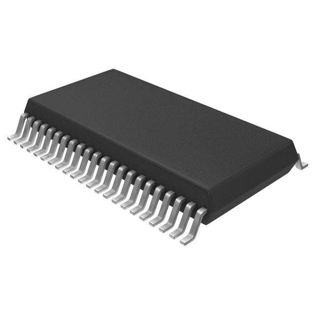
| 描述 | IC 3-TO-1 DVI/HDMI SWITCH 80TQFP视频开关 IC 3-TO-1 DVI/HDMI Sw |
| 产品分类 | |
| 品牌 | Texas Instruments |
| 产品手册 | |
| 产品图片 |
|
| rohs | 符合RoHS无铅 / 符合限制有害物质指令(RoHS)规范要求 |
| 产品系列 | 开关 IC,视频开关 IC,Texas Instruments TMDS341APFCR- |
| 数据手册 | |
| 产品型号 | TMDS341APFCR |
| 产品目录页面 | |
| 产品种类 | 视频开关 IC |
| 传播延迟时间 | 800 ps |
| 供应商器件封装 | 80-TQFP(12x12) |
| 其它名称 | 296-19741-6 |
| 包装 | Digi-Reel® |
| 单位重量 | 373.600 mg |
| 商标 | Texas Instruments |
| 安装类型 | 表面贴装 |
| 安装风格 | SMD/SMT |
| 封装 | Reel |
| 封装/外壳 | 80-TQFP |
| 封装/箱体 | TQFP-80 |
| 工厂包装数量 | 1000 |
| 应用 | 3:1 可切换 DVI/HDMI 接收器 |
| 接口 | DVI,HDMI |
| 最大功率耗散 | 657 mW |
| 最大工作温度 | + 70 C |
| 最小工作温度 | 0 C |
| 标准包装 | 1 |
| 电压-电源 | 3 V ~ 3.6 V |
| 系列 | TMDS341A |


- 商务部:美国ITC正式对集成电路等产品启动337调查
- 曝三星4nm工艺存在良率问题 高通将骁龙8 Gen1或转产台积电
- 太阳诱电将投资9.5亿元在常州建新厂生产MLCC 预计2023年完工
- 英特尔发布欧洲新工厂建设计划 深化IDM 2.0 战略
- 台积电先进制程称霸业界 有大客户加持明年业绩稳了
- 达到5530亿美元!SIA预计今年全球半导体销售额将创下新高
- 英特尔拟将自动驾驶子公司Mobileye上市 估值或超500亿美元
- 三星加码芯片和SET,合并消费电子和移动部门,撤换高东真等 CEO
- 三星电子宣布重大人事变动 还合并消费电子和移动部门
- 海关总署:前11个月进口集成电路产品价值2.52万亿元 增长14.8%


PDF Datasheet 数据手册内容提取
TMDS341A www.ti.com SLLS702B–MAY2006–REVISEDMARCH2007 3-TO-1 DVI/HDMI SWITCH FEATURES Exceeds5kV • CompatiblewithHDMI1.3a • 3.3-VSupplyOperation • Supports2.25GbpsSignalingRatefor480i/p, • 80-PinTQFPPackage 720i/p,and1080i/pResolutionsupto12-Bit • ROHSCompatibleand260(cid:176) CReflowRated ColorDepth • EachPortSupportsHDMIorDVIInputs APPLICATIONS • IsolatedDigitalDisplayControl(DDC)Busfor • SwitchingFromThreeDigital-Video(DVI)or UnusedPorts Digital-AudioVisual(HDMI)Sources • 5-VTolerancetoallDDCandHPD_SINK • DigitalTV Inputs • DigitalProjector • IntegratedReceiverTermination • AudioVideoReceiver • Inter-PairOutputSkew<100ps • Intra-PairSkew<50ps • 8-dBReceiverEqualizationtoCompensatefor 5-mDVICableLosses • HighImpedanceOutputsWhenDisabled • TMDSInputsHBMESDProtection DESCRIPTION The TMDS341A is a 3-port digital video interface (DVI) or high-definition multimedia interface (HDMI) switch that allows up to 3 DVI or HDMI ports to be switched to a single display terminal. Four TMDS channels, one hot plug detector, and an I2C interface are supported on each port. Each TMDS channel allows signaling rates up to 2.25 Gbps. The active source is selected by configuring source selectors, S1, S2, and S3. The selected TMDS inputs from each port are switched through a 3-to-1 multiplexer. The I2C interface of the selected input port is linked to the I2C interface of the output port, and the hot plug detector (HPD) of the selected input port is output to HPD_SINK.Fortheunusedports,theI2Cinterfacesareisolated,andtheHPDpinsarekeptlow. Termination resistors (50-W ), pulled up to V , are integrated at each receiver input pin. External terminations CC are not required. A precision resistor is connected externally from the VSADJ pin to ground for setting the differential output voltage to be compliant with the TMDS standard. When the output is connected to a standard TMDSterminationandOEishigh,theoutputishighimpedance. The TMDS341A provides fixed 8-dB input equalization and selectable 3-dB output de-emphasis to optimize system performance through 5-meter or longer DVI compliant cables. The device is characterized for operation from0(cid:176) Cto70(cid:176) C. TypicalApplication DVD Player Digital TV PC or TMDS Game 341A Machine STB Pleasebeawarethatanimportantnoticeconcerningavailability,standardwarranty,anduseincriticalapplicationsofTexas Instrumentssemiconductorproductsanddisclaimerstheretoappearsattheendofthisdatasheet. PRODUCTIONDATAinformationiscurrentasofpublicationdate. Copyright©2006–2007,TexasInstrumentsIncorporated Products conform to specifications per the terms of the Texas Instruments standard warranty. Production processing does not necessarilyincludetestingofallparameters.
TMDS341A www.ti.com SLLS702B–MAY2006–REVISEDMARCH2007 Thesedeviceshavelimitedbuilt-inESDprotection.Theleadsshouldbeshortedtogetherorthedeviceplacedinconductivefoam duringstorageorhandlingtopreventelectrostaticdamagetotheMOSgates. FUNCTIONALBLOCKDIAGRAM B A B A B A B A 1 1 1 1 1 1 1 1 1 1 2 2 3 3 4 4 V C EQRx w/ INTR EQRx w/ INTR EQRx w/ INTR EQRx w/ INTRC (3.3 V ) PRE VCC (3.3 V) VSADJ RINT A24 Y4 Rx w/ TMDS EQ B24 3−to−1 MUX Drive VCC Z4 RINT A23 Rx w/ EQ B23 Y3 VCC RINT TMDS A22 Drive Rx w/ Z3 EQ B22 VCC RINT Y2 A21 Rx w/ TMDS EQ Drive B21 Z2 VCC (3.3 V) RINT Y1 A34 TMDS Rx w/ Drive B34 EQ Z1 VCC RINT OE A33 Rx w/ EQ B33 VCC S1 RINT S2 A32 Rx w/ S3 EQ B32 VCC RINT A31 Rx w/ B31 EQ HPD1 HPD2 Control Logic HPD_SINK HPD3 SCL1 SCL_SINK SDA1 SDA_SINK SCL2 SDA2 SCL3 SDA3 2 SubmitDocumentationFeedback
TMDS341A www.ti.com SLLS702B–MAY2006–REVISEDMARCH2007 PFCPACKAGE (TOPVIEW) C ND 43 43 CC 33 33 ND 32 32 CC 31 31 ND L3C DA3 PD3 CC E C N G A B V A B G A B V A B G S S H V O N 60 59 58 57 56 55 54 53 52 51 50 49 48 47 46 45 44 43 42 41 VCC 61 40 HPD_SINK HPD2 62 39 SDA_SINK SDA2 63 38 SCL_SINK SCL2 64 37 GND GND 65 36 GND GND 66 35 Z1 B21 67 34 Y1 A21 68 33 VCC VCC 69 32 Z2 B22 70 31 Y2 A22 71 30 GND GND 72 29 Z3 B23 73 28 Y3 A23 74 27 VCC VCC 75 26 Z4 B24 76 25 Y4 A24 77 24 GND GND 78 23 S3 VCC 79 22 S2 HPD1 80 21 S1 1 2 3 4 5 6 7 8 9 10 11 12 13 14 15 16 17 18 19 20 NC SDA1 SCL1 GND B11 A11 VCC B12 A12 GND B13 A13 VCC B14 A41 GND VCC VSADJ ERP NC SubmitDocumentationFeedback 3
TMDS341A www.ti.com SLLS702B–MAY2006–REVISEDMARCH2007 TERMINALFUNCTIONS TERMINAL I/O DESCRIPTION NAME NO. A11,A12,A13,A14 6,9,12,15 I Port1TMDSpositiveinputs A21,A22,A23,A24 68,71,74,77 I Port2TMDSpositiveinputs A31,A32,A33,A34 49,52,55,58 I Port3TMDSpositiveinputs B11,B12,B13,B14 5,8,11,14 I Port1TMDSnegativeinputs B21,B22,B23,B24 67,70,73,76 I Port2TMDSnegativeinputs B31,B32,B33,B34 48,51,54,57 I Port3TMDSnegativeinputs 4,10,1624,30, GND 36,37,47,53, Ground 59,65,66,72,78 HPD1 80 O Port1hotplugdetectoroutput HPD2 62 O Port2hotplugdetectoroutput HPD3 44 O Port3hotplugdetectoroutput Sinksidehotplugdetectorinput HPD_SINK 40 I High:5-VpowersignalassertedfromsourcetosinkandEDIDisready Low:No5-Vpowersignalassertedfromsourcetosink,orEDIDisnotready NC 1,20,41,60 Noconnect OE 42 I Outputenable,activelow Outputde-emphasisadjustment PRE 19 I High:3dB Low:0dB SCL1 3 I/O Port1DDCbusclockline SCL2 64 I/O Port2DDCbusclockline SCL3 46 I/O Port3DDCbusclockline SCL_SINK 38 I/O SinksideDDCbusclockline SDA1 2 I/O Port1DDCbusdataline SDA2 63 I/O Port2DDCbusdataline SDA3 45 I/O Port3DDCbusdataline SDA_SINK 39 I/O SinksideDDCbusdataline S1,S2,S3 21,22,23 I Sourceselectorinput 7,13,1727,33, V 43,50,5661,69, Powersupply CC 75,79 VSADJ 18 I TMDScompliantvoltageswingcontrol Y1,Y2,Y3,Y4 34,31,28,25 O TMDSpositiveoutputs Z1,Z2,Z3,Z4 35,32,29,26 O TMDSnegativeoutputs 4 SubmitDocumentationFeedback
TMDS341A www.ti.com SLLS702B–MAY2006–REVISEDMARCH2007 Table1.SourceSelectionLookup(1) CONTROLPINS I/OSELECTED HOTPLUGDETECTSTATUS SCL_SINK S1 S2 S3 Y/Z HPD1 HPD2 HPD3 SDA_SINK SCL1 H x x A1/B1 HPD_SINK L L SDA1 SCL2 L H x A2/B2 L HPD_SINK L SDA2 SCL3 L L H A3/B3 L L HPD_SINK SDA3 L L L None(Z) None(Z) L L L (1) H:Logichigh;L:Logiclow;X:Don'tcare;Z:Highimpedance SubmitDocumentationFeedback 5
TMDS341A www.ti.com SLLS702B–MAY2006–REVISEDMARCH2007 EQUIVALENT INPUT AND OUTPUT SCHEMATIC DIAGRAMS TMDS Input Stage TMDS Output Stage Y Vcc 25W Z 25W 50W 50W A B 10 mA Control Input Stage HPD output stage Vcc Vcc OE HPD_SINK 400W HPD1 PRE HPD2 S1, S2, S3 HPD3 DDC pass gate Vcc SCL/SCA SCL/SCA Source Sink 8V 8V ORDERINGINFORMATION(1) PARTNUMBER PARTMARKING PACKAGE TMDS341APFC TMDS341A 80-PINTQFP TMDS341APFCR TMDS341A 80-PINTQFPTape/Reel (1) Forthemostcurrentpackageandorderinginformation,seethePackageOptionAddendumattheendofthisdocument,orseetheTI websiteatwww.ti.com. 6 SubmitDocumentationFeedback
TMDS341A www.ti.com SLLS702B–MAY2006–REVISEDMARCH2007 ABSOLUTE MAXIMUM RATINGS overoperatingfree-airtemperaturerange(unlessotherwisenoted)(1) UNIT Supplyvoltagerange,V (2) –0.5Vto4V CC Anm(3),Bnm 2.5Vto4V Voltagerange Ym,Zm,VSADJ,PRE,Sn,OE,HPDn –0.5Vto4V SCLn,SCL_SINK,SDAn,SDA_SINK,HPD_SINK –0.5Vto6V Anm,Bnm 5kV Humanbodymodel(4) Electrostatic Allpins 4kV discharge Charged-devicemodel(5)(allpins) 1000V Machinemodel (6)(allpins) 250V SeeDissipationRating Continuouspowerdissipation Table (1) Stressesbeyondthoselistedunderabsolutemaximumratingsmaycausepermanentdamagetothedevice.Thesearestressratings onlyandfunctionaloperationofthedeviceattheseoranyotherconditionsbeyondthoseindicatedunderrecommendedoperating conditionsisnotimplied.Exposuretoabsolute-maximum-ratedconditionsforextendedperiodsmayaffectdevicereliability. (2) Allvoltagevalues,exceptdifferentialI/Obusvoltages,arewithrespecttonetworkgroundterminal. (3) n=1,2,3;m=1,2,3,4 (4) TestedinaccordancewithJEDECStandard22,TestMethodA114-B (5) TestedinaccordancewithJEDECStandard22,TestMethodC101-A (6) TestedinaccordancewithJEDECStandard22,TestMethodA115-A DISSIPATION RATINGS PACKAGE TA£ 25(cid:176) C DEARBAOTIVNEGTFA=C2T5O(cid:176) RC (1) POWTAER=7R0A(cid:176) CTING A 80-TQFP 1342mW 13.42mW/(cid:176) C 738mW (1) Thisistheinverseofthejunction-to-ambientthermalresistancewhenboard-mountedandwithnoairflow. RECOMMENDED OPERATING CONDITIONS MIN NOM MAX UNIT V Supplyvoltage 3 3.3 3.6 V CC T Operatingfree-airtemperature 0 70 (cid:176) C A TMDSDIFFERENTIALPINS(A/B) V Receiverpeak-to-peakdifferentialinputvoltage 150 1560 mVp-p ID V Inputcommonmodevoltage V –0.4 V +0.01 V IC CC CC R ResistorforTMDScompliantvoltageswingrange 4.6 4.64 4.68 kW VSADJ AV TMDSoutputterminationvoltage,seeFigure1 3 3.3 3.6 V CC R Terminationresistance,seeFigure1 45 50 55 W T Signalingrate 0 2.25 Gbps CONTROLPINS(PRE;S,OE) V LVTTLHigh-levelinputvoltage 2 V V IH CC V LVTTLLow-levelinputvoltage GND 0.8 V IL DDCI/OPINS(SCL,SCL_SINK,SDA,SDA_SINK) V Inputvoltage GND 5.5 V I(DDC) STATUSPINS(HPD_SINK) V LVTTLHigh-levelinputvoltage 2 5.3 V IH V LVTTLLow-levelinputvoltage GND 0.8 V IL SubmitDocumentationFeedback 7
TMDS341A www.ti.com SLLS702B–MAY2006–REVISEDMARCH2007 ELECTRICAL CHARACTERISTICS overrecommendedoperatingconditions(unlessotherwisenoted) PARAMETER TESTCONDITIONS MIN TYP(1) MAX UNIT VIH=VCC,VIL=VCC–0.4V,RVSADJ=4.64kW , ICC Supplycurrent RAmT=/B5m0=W 1,.A6V5CGCb=ps3.H3DVMIdatapattern,m=2,3,4 190 230 mA A1/B1=165MHzclock VIH=VCC,VIL=VCC–0.4V,RVSADJ=4.64kW , PD Powerdissipation RAmT=/B5m0=W 1,.A6V5CGCb=ps3.H3DVMIdatapattern,m=2,3,4 394 657 mW A1/B1=165MHzclock TMDSDIFFERENTIALPINS(A/B;Y/Z) VOH Single-endedhigh-leveloutputvoltage AVCC–10 AVCC+10 mV VOL Single-endedlow-leveloutputvoltage AVCC–600 AVCC–400 mV Vswing Single-endedoutputswingvoltage 400 600 mV VOD(O) Overshootofoutputdifferentialvoltage SReTe=F5i0guWre,P2R,AEV=CC0=V3.3V, 6% 15% 2· Vswing VOD(U) Undershootofoutputdifferentialvoltage 12% 25% 2· Vswing D VOC(SS) Couhtapnugtevoinltasgteeabdeyt-wsteaetencloogmicmsotant-emsode 0.5 5 mV I(O)OFF Single-endedstandbyoutputcurrent 0AVVC£CV=C3C.3£ V1,.5RVT,=50W –10 10 µA |I(OS)| Shortcircuitoutputcurrent SeeFigure3 12 mA VODE(SS) Sdete-eamdyphstaastiesoutputdifferentialvoltagewith SAeme/BFmigu=re2540,PMRbEps=HVDCMC,Idatapattern,m=2,3,4 560 840 mVp-p VODE(pp) Peak-to-peakoutputdifferentialvoltage A1/B1=25MHzclock 800 1200 mVp-p Single-endedinputvoltageunderhigh VI(open) impedanceinputoropeninput II=10µA VCC–10 VCC+10 mV RINT Inputterminationresistance VIN=2.9V 45 50 55 W DDCI/OPINS(SCL,SCL_SINK,SDA,SDA_SINK) |Ilkg| Inputleakagecurrent VI=0.1VCCto0.9VCCtoisolatedDDCports 0.1 2 µA CIO Input/outputcapacitance VI=0V 7.5 pF RON Switchresistance IO=3mA,VO=0.4V 25 50 W VPASS Switchoutputvoltage VI=3.3V,IO=100µA 1.5(2) 2.0 2.5(3) V STATUSPINS(HPD) VOH(TTL) TTLHigh-leveloutputvoltage IOH=–8mA 2.4 V VOL(TTL) TTLLow-leveloutputvoltage IOL=8mA 0.4 V CONTROLPINS(PRE,S,OE) |IIH| High-leveldigitalinputcurrent VIH=2VorVCC 0.1 2 µA |IIL| Low-leveldigitalinputcurrent VIL=GNDor0.8V 0.1 2 µA STATUSPINS(HPD_SINK) VIH=5.3V 23 100 |IIH| High-leveldigitalinputcurrent µA VIH=2VorVCC 0.1 2 |IIL| Low-leveldigitalinputcurrent VIL=GNDor0.8V 0.1 2 µA (1) Alltypicalvaluesareat25(cid:176) Candwitha3.3-Vsupply. (2) Thevalueistestedinfulltemperaturerangeat3.0V. (3) Thevalueistestedinfulltemperaturerangeat3.6V. 8 SubmitDocumentationFeedback
TMDS341A www.ti.com SLLS702B–MAY2006–REVISEDMARCH2007 SWITCHING CHARACTERISTICS overrecommendedoperatingconditions(unlessotherwisenoted) PARAMETER TESTCONDITIONS MIN TYP(1) MAX UNIT TMDSDIFFERENTIALPINS(Y/Z) tPLH Propagationdelaytime,low-to-high-leveloutput 250 800 ps tPHL Propagationdelaytime,high-to-low-leveloutput 250 800 ps tr Differentialoutputsignalrisetime(20%-80%) 75 240 ps tf Differentialoutputsignalfalltime(20%-80%) SeeFigure2,AVCC=3.3V, 75 240 ps tsk(p) Pulseskew(|tPHL–tPLH|) RT=50W ,PRE=0V 7 50 ps tsk(D) Intra-pairdifferentialskew,seeFigure5 23 50 ps tsk(o) Inter-pairchannel-to-channeloutputskew(2) 100 ps tsk(pp) Part-to-partskew(3) 200 ps tjit(pp) Peak-to-peakoutputjitterfromY/Z(1)residualjitter SeeFigure8,PRE=0V 15 30 ps Am/Bm=1.65GbpsHDMIdatapattern, tjit(pp) Peak-to-peakoutputjitterfromY/Z(2:4)residualjitter m=2,3,4 18 50 ps A1/B1=165MHzclock tjit(pp) Peak-to-peakoutputjitterfromY/Z(1)residualjitter SeeFigure8,PRE=0V 20 22 ps Am/Bm=2.25GbpsHDMIdatapattern, tjit(pp) Peak-to-peakoutputjitterfromY/Z(2:4)residualjitter m=2,3,4 38 78 ps A1/B1=225MHzclock SeeFigure4,PRE=VCC Am/Bm=250MbpsHDMIdatapattern, tPRE De-emphasisduration m=2,3,4 240(4) ps A1/B1=25MHzclock tSX Selecttoswitchoutput 6 10 ns ten Enabletime SeeFigure6 6 10 ns tdis Disabletime 6 10 ns DDCI/OPINS(SCL,SCL_SINK,SDA,SDA_SINK) PropagationdelayfromSCLntoSCL_SINKorSDAnto tpd(DDC) SDA_SINKorSDA_SINKtoSDAn SeeFigure7,CL=10pF 0.4 2.5 ns CONTROLANDSTATUSPINS(S,HPD_SINK,HPD) tpd(HPD) Propagationdelay(fromHPD_SINKtotheactiveportofHPD) 2 6.0 ns SeeFigure7,CL=10pF tsx(HPD) Switchtime(fromportselecttothelatestvalidstatusofHPD) 3 6.5 ns (1) Alltypicalvaluesareat25(cid:176) Candwitha3.3-Vsupply. (2) t isthemagnitudeofthedifferenceinpropagationdelaytimesbetweenanyspecifiedterminalsofchannel2to4ofadevicewhen sk(o) inputsaretiedtogether. (3) t isthemagnitudeofthedifferenceinpropagationdelaytimesbetweenanyspecifiedterminalsofchannel2to4oftwodevices,or sk(pp) betweenchannel1oftwodevices,whenbothdevicesoperatewiththesamesource,thesamesupplyvoltages,atthesame temperature,andhaveidenticalpackagesandtestcircuits. (4) Thetypicalvalueisensuredbysimulation. SubmitDocumentationFeedback 9
TMDS341A www.ti.com SLLS702B–MAY2006–REVISEDMARCH2007 PARAMETER MEASUREMENT INFORMATION AVcc RT RT ZO = RT TMDS TMDS Driver Receiver ZO = RT Figure1.TerminationforTMDSOutputDriver Vcc R R INT INT RT Y A VA VID RTeMcDeSiver TDMriDveSr 0.5 CpFL VY RT AVcc B Z V V B VID= V A − VB Vswing = V Y − VZ Z DC Coupled AC Coupled V Vcc Vcc+0.2 V A V B Vcc−0.4 V Vcc−0.2 V V 0.4 V ID V V ID ID(pp) 0 V −0.4 V tPHL tPLH 100% 80% VOD(O) 0V Differential VOD(pp) 20% 0% tf tr VOD(U) V (cid:1) OC V OC(SS) NOTE: All input pulses are supplied by a generator having the following characteristics: t or t < 100 ps, 100 MHz from r f Agilent 81250. C includes instrumentation and fixture capacitance within 0.06 m of the D.U.T. Measurement L equipmentprovidesabandwidthof20GHzminimum. Figure2.TimingTestCircuitandDefinitions 10 SubmitDocumentationFeedback
TMDS341A www.ti.com SLLS702B–MAY2006–REVISEDMARCH2007 PARAMETER MEASUREMENT INFORMATION (continued) 50 (cid:1) IOS TMDS Driver 50 (cid:1) + _ 0 V or 3.6 V Figure3.ShortCircuitOutputCurrentTestCircuit 1 bit 1 to N bit VOD(pp) VODE(SS) 80% 20% t PRE Figure4.De-EmphasisOutputVoltageWaveformsandDurationMeasurementDefinitions VY VOH 50% VZ VOL tsk(D) Figure5.DefinitionofIntra-PairDifferentialSkew SubmitDocumentationFeedback 11
TMDS341A www.ti.com SLLS702B–MAY2006–REVISEDMARCH2007 PARAMETER MEASUREMENT INFORMATION (continued) Input−1 A Kept B High Input−2/Input−3 A Kept Low B 3.3 V S1 Clocking VCC 2 0 V S2 or S3 Kept High tsx tsx Y 75 mV Hi−Z 75 mV Output Z −75 mV −75 mV 3.3 V OE VCC 2 0 V tdis ten Figure6.TMDSOutputsControlTimingDefinitions HPD_SINK VCC 2 HPD1 VCC 2 0.4 V tsx(HPD) tpd(HPD) tpd(HPD) 2.4 V HPD2 HPD3 0 V S1 VCC 2 S2 S3 0 V SDA_SINK VCC 2 tpd(DDC) tpd(DDC) SDA1 VCC 2 SDA2 SDA3 Figure7.HPDTimingDefinitions 12 SubmitDocumentationFeedback
TMDS341A www.ti.com SLLS702B–MAY2006–REVISEDMARCH2007 PARAMETER MEASUREMENT INFORMATION (continued) AVcc RT RT Data + Coax SMA R+X MU OUT Trans<m2i”s s5i0onW Line SMA Coax Data − Coax SMA EQ X 0dB Trans<m2i”s s5i0onW Line SMA Coax Video Patterm Jitter Test Generator 5HmD M28I ACWabGle TMDS341A AVcc Instrument 1000 mVpp RT RT Differential Clk+ Coax SMA R+X MU OUT Trans<m2i”s 5si0onW Line SMA Coax Clk− Coax SMA EQ X 0dB Trans<m2i”s 5si0onW Line SMA Coax Jitter Test Instrument TP1 TP2 TP3 A. AlljittersaremeasuredinBERof10-12 B. The residual jitter reflects the total jitter measured at the TMDS341A output, TP3, subtract the total jitter from the signalgenerator,TP1 Figure8.JitterTestCircuit Figure 9 shows the frequency loss response from a 5m 28AWG HDMI cable and a 5m 28AWG DVI cable. The TMDS341A built-in passive input equalizer compensates for ISI. For an 8-dB loss HDMI cable, the TMDS341A typicallyreducesjitterby60psfromthedeviceinputtothedeviceoutput. TMDS341 input equalization gain vs. 5m DVI/HDMI cable response 0 Inversed TMDS341 EQ Gain −2 −4 −6 28 AWG 5m HDMI Cable B d −8 − n ai −10 G −12 28 AWG 5m DVI Cable −14 −16 −18 0 200 400 600 800 1000 1200 1400 1600 1800 2000 f − Frequency − MHz Figure9.S-ParameterPlotsof5-mDVIandHDMICables SubmitDocumentationFeedback 13
TMDS341A www.ti.com SLLS702B–MAY2006–REVISEDMARCH2007 TYPICAL CHARACTERISTICS SUPPLYCURRENT SUPPLYCURRENT vs vs FREQUENCY FREE-AIRTEMPERATURE 230 195 V =AV = 3.3 V, T = 25 C, CC CC A V =AV = 3.3 V, 220 TP1 VID(PP)= 800 mVp-p, RVSADJ= 4.64 KW TPC1C V CC= 800 mV, R = 4.64 KW PRE =OE= Low 193 Input (ID2:(P4P) )2.25 Gbps HDVSMAID DJata Pattern Input (2:4) HDMI Data Pattern, 250 Mbps - 2.25 Gbps A Input (1) Clock, 25 MHz - 165 Mhz A Input (1) 165 MHzClock m 210 m nt - nt - e e 191 urr 200 urr C C y y ppl 190 ppl 189 u u S S - - CC 180 CC I I 187 170 160 185 0 10 20 30 40 50 60 70 25 45 65 75 85 105 145 165 T - Free-Air Temperature - C A f - Frequency - MHz Figure10. Figure11. RESIDUALDETERMINISTICJITTER RESIDUALPEAK-TO-PEAKJITTER vs vs DATARATE CLOCKFREQUENCY 8 3 al VCC=AVCC= 3.3 V, TA= 25°C, VCC=AVCC= 3.3 V, TA= 25°C, rv TP1 VID(PP)= 800 mV, RVSADJ= 4.64 KW al TP1 VID(PP)= 800 mVp-p, RVSADJ= 4.64 KW nte PRE =OE= Low, Source jitter = 180 ps erv PRE =OE= Low, Source jitter = 150 ps % Unit I 6 3 m HDMI Cable Unit Int 2 3 m HDMI Cable c Jitter - 4 1 m HDMI Cable Jitter - % 5 m HD1M mI C HaDblMeI Cable sti k ni 5 m HDMI Cable ea mi P r k- 1 e a Det 2 Pe Residual Residual 0 0 200 250 450 650 750850 10501250 1450 1650 20 25 45 65 75 85 105 125 145 165 Data Rate - Mbps Clock Frequency - MHz Figure12. Figure13. 14 SubmitDocumentationFeedback
TMDS341A www.ti.com SLLS702B–MAY2006–REVISEDMARCH2007 TYPICAL CHARACTERISTICS (continued) RESIDUALDETERMINISTICJITTER RESIDUALPEAK-TO-PEAKJITTER vs vs DIFFERENTIALINPUTVOLTAGE DIFFERENTIALINPUTVOLTAGE 10 4 val 9 270 Mbps al 3 148.5 MHz Unit Inter 78 742.5 Mbps nit Interv 012 stic Jitter - % 3456 1485 Mbps ak Jitter - % U ----4321 74.25 MHz 27 MHz etermini 12 Peak-Pe ---576 Residual D --210 VRCVCSA=DAJV=C 4C.6=4 3K.3W V,P, TRAE= = 2O5°EC,= Low Residual -1--098 VRCVCSA=DAJV=C 4C.6=4 3K.3W V,P, TRAE= = 2O5°EC,= Low -3 -11 150 350 550 750 950 1150 1350 1550 150 350 550 750 950 1150 1350 1550 Peak-to-Peak Differential Input Voltage - mVp-p Peak-to-Peak Differential Input Voltage - mVp-p Figure14. Figure15. RESIDUALDETERMINISTICJITTER RESIDUALPEAK-TO-PEAKJITTER vs vs FR4PCBTRACE(at3dBPre-Emphasis) FR4PCBTRACE(at3dBPre-Emphasis) 15 4 Unit Interval 11112431 VTP5-PRCm1CE 2V==8I ADHA(ViPWgCPhCG),= =H O 83DE0.M30= IVm LC, VoTa,wA bR=,leV 2S5A°DCJ,= 4.64 KW nit Interval 3.5 VTPPRC1CE V==I ADH(ViPgCPhC),==O 83E0.30= VmL,o VTw,A R,= 5V 2-Sm5A° DC2J8,=A W4.6G4 HKDWMI Cable c Jitter - % 1890 1485 Mbps Jitter - % U 22..05 148.5 MHz sti 7 ak mini 6 k-Pe al Deter 354 742.5 Mbps ual Pea 74.25 MHz u d sid 2 270 Mbps esi 0.5 27 MHz e R R 1 0 0 5 7 11 15 19 5 7 11 15 19 FR4 PCB Trace - Inch FR4 PCB Trace - Inch Figure16. Figure17. SubmitDocumentationFeedback 15
TMDS341A www.ti.com SLLS702B–MAY2006–REVISEDMARCH2007 TYPICAL CHARACTERISTICS (continued) RESIDUALPEAK-TO-PEAKJITTER RESIDUALPEAK-TO-PEAKJITTER (DataChannels) (ClockChannel) vs vs CLOCKFREQUENCY CLOCKFREQUENCY 20 5 Channels 2, 3, 4, Channel 1, al VCC=AVCC= 3.3 V, TA= 25°C,RVSADJ= 4.64 KW, val VCC=AVCC= 3.3 V, TA= 25°C,RVSADJ= 4.64 KW, nit Interv 16 771P220R008Epp0 p//=11 008O88-EB00iii=t 81 =L-2 Bo-1Biw4ti 8,t= 5T= 7 p M4111b2 1V.p53Is D.M,7(P5bP pM)s=b, p1s0,00 mVp-p, Unit Inter 4 PRE =OE= Low,Tp1 VID(PP)= 1000 mVp-p U 1080p 12-Bit = 2227.5 Mbps % r - % 12 er - 3 k Jitte 3 m 30AWG ak Jitt ea 8 Pe 2 3 m 30AWG k-P ak- a e e P ual P 4 5 m 28AWG dual 1 sid esi 5 m 28AWG e R R 0 0 750 950 1150 1485 1650 1850 2250 75 95 115 148.5 165 185 225 Clock Frequency -MHz ClockFrequency-MHz Figure18. Figure19. 16 SubmitDocumentationFeedback
TMDS341A www.ti.com SLLS702B–MAY2006–REVISEDMARCH2007 TYPICAL CHARACTERISTICS (continued) HDMI Cables Running at 165-MHz Pixel Clock TP1 TP2 TP3 TMDS341ATest Board Video 28AWG HDMI Cable TMDS Format 341A Generator Figure20.1-mand5-mHDMICableTestPointConfiguration 1-mCableLengthEyePatterns Figure21.ClockatTP1 Figure22.ClockatTP2 Figure23.ClockatTP3 Figure24.DataatTP1 Figure25.DataatTP2 Figure26.DataatTP3 SubmitDocumentationFeedback 17
TMDS341A www.ti.com SLLS702B–MAY2006–REVISEDMARCH2007 TYPICAL CHARACTERISTICS (continued) 5-mCableLengthEyePatterns Figure27.ClockatTP1 Figure28.ClockatTP2 Figure29.ClockatTP3 Figure30.DataatTP1 Figure31.DataatTP2 Figure32.DataatTP3 (DC-CoupledInput) Figure33.DataatTP3 (AC-CoupledInput) 18 SubmitDocumentationFeedback
TMDS341A www.ti.com SLLS702B–MAY2006–REVISEDMARCH2007 APPLICATION INFORMATION Supply Voltage All V pins can be tied to a single 3.3-V power source. A 0.01-µF capacitor is connected from each V pin CC CC directlytogroundtofiltersupplynoise. TMDS Inputs Standard TMDS terminations are integrated on all TMDS inputs. External terminations are not required. Each input channel contains an 8-dB equalization circuit to compensate for cable losses. The voltage at the TMDS input pins must be limited per the absolute maximum ratings. An unused input should not be connected to groundasthiswouldresultinexcessivecurrentflowdamagingthedevice. TMDS Input Fail-Safe TMDS input pins do not incorporate fail-safe circuits. An unused input channel can be externally biased to prevent output oscillation. One pin can be left open with the other grounded through a 1-kW resistor as shown in Figure34. VCC TMDS341A RINT RINT RT A TMDS TMDS Y Receiver Driver AVCC B Z RT Figure34.TMDSInputFail-SafeRecommendation TMDS Outputs A 1% precision resister, 4.64-kW , connected from VSADJ to ground is recommended to allow the differential output swing to comply with TMDS signal levels. The differential output driver provides a typical 10-mA current sinkcapability,whichprovidesatypical500-mVvoltagedropacrossa50-W terminationresistor. VCC AVCC TMDS341A RT RT ZO = RT TMDS TMDS Receiver Driver ZO = RT GND Figure35.TMDSDriverandTerminationCircuit As shown in Figure 35, if V (TMDS341A supply) and AV (sink termination supply) are powered, the TMDS CC CC outputsignalsarehighimpedancewhenOEishigh.Normaloperationiswithbothsuppliesactive. Also shown in Figure 35, if V is on and AV is off, the TMDS outputs source a typical 5-mA current through CC CC each termination resistor to ground. The terminations consume a total of 10 mW of power independent of the OElogicalselection.WhenAV ispoweredon,normaloperation(OEcontrolsoutputimpedance)isresumed. CC SubmitDocumentationFeedback 19
TMDS341A www.ti.com SLLS702B–MAY2006–REVISEDMARCH2007 APPLICATION INFORMATION (continued) When the power source of the device, V , is off and the power source to termination, AV , is on, the output CC CC leakagecurrent(I )specificationensuresleakagecurrentislimitedto10-µAorless. o(off) The PRE pin provides 3-dB de-emphasis, allowing output signal pre-conditioning to offset interconnect losses from the TMDS341A outputs to a TMDS receiver. PRE is recommended to be low to the circuit design of a stand-aloneswitchbox. HPD Pins The input of the HPD_SINK is 5-V tolerant, allowing direct connection to 5-V signals. The HPD pin output resistance is 35-W typically. A 1-kW 10% resistor is recommended to be connected from an HPD pin at the TMDS341AtotheHPDpinoftheHDMIconnector. DDC Channels The DDC channels are designed with a bi-directional pass gate, providing 5-V signal tolerance. The 5-V tolerance allows direct connection to a standard I2C bus. The level shifter between 3.3 V and 5 V I2C interface canbeeliminated. Configuring the TMDS341A as a 2:1 Switch The TMDS341A can be configured as a 2-to-1 switch by pulling the source selector pin (S1, S2, S3) of the non-activeportlowandleavingthecorrespondingTMDSinputs,SCL,SDA,andHPDpinsopen. Layout Considerations The high-speed TMDS inputs are the most critical paths for the TMDS341A. There are several considerations to minimizediscontinuitiesonthesetransmissionlinesbetweentheconnectorsandthedevice: • Maintain100-W differentialtransmissionlineimpedanceintoandoutoftheTMDS341A • Keepanuninterruptedgroundplanebeneaththehigh-speedI/Os • Keeptheground-pathviastothedeviceascloseaspossibletoallowtheshortestreturncurrentpath • LayoutoftheTMDSdifferentialinputsshouldbewiththeshorteststubsfromtheconnectors Connecting Cables Longer Than 5 m When using the TMDS341A with cables longer than 5 m, the impact to the TMDS signal path as well as the DDCsignalpathmustbeconsidered. TMDSSignalPath The TMDS341A receiver equalization circuit provides the capability of compensating inter-symbol interference (ISI) losses in a 5-m 28-AWG DVI cable. Typical cable measurements indicate that the TMDS341A can drive a 5-m 28-AWG HDMI cable and pass the eye mask at the output of a HDMI source (TP1) and a 10-m 28-AWG HDMI cable and pass the eye mask at the input of a HDMI sink (TP2). Figure 36 through Figure 39 show the eyemaskmeasurementresults. Figure36.EyeDiagramatOutput5-m28-AWGCablevs Figure37.EyeDiagramRecoveredbyTMDS341AvsTP1 TP1EyeMask EyeMask 20 SubmitDocumentationFeedback
TMDS341A www.ti.com SLLS702B–MAY2006–REVISEDMARCH2007 APPLICATION INFORMATION (continued) Figure38.EyeDiagramatOutput10-m28-AWGCable Figure39.EyeDiagramRecoveredbyTMDS341AvsTP2 vsTP2EyeMask EyeMask DDCSignalPath Observed I2C bus voltage is dependent on bus resistance, capacitance, and time. The transient bus voltage, whenchargingfromalowstatetoahighstate,canbecalculatedusingequation(1). V(t)=V (1–e–t/RC) (1) DD Where: tisthetimesincethechargingstarted V isthepull-upterminationvoltage DD RisthetotalresistanceontheI2Clink CisthetotalcapacitanceontheI2Clink In the I2C bus specification, version 2.1, the high-level threshold voltage is V = 0.7 V , and the low-level IH DD thresholdvoltageisV =0.3V . IL DD Fromequation(1),thetimestochargefromabusvoltageof0VtotheV andV levelsare: IH IL t =1.204×RC IH t =0.357×RC IL Thebusrisetime(from0.3V to0.7V )isthengivenbyequation(2): DD DD t =t –t =0.847×RC (2) r(30-70) IH IL The TMDS341A can be easily applied in stand-alone switch boxes and digital displays. The following sections showthebuslengthsthatcanbesupportedineachcase. MaximumBusLengthsforSwitchApplications Figure 40 shows the TMDS341A being used as a stand-alone switch. Both pull-up resistors are decided by the sourceandsinkequipment.A1.5-kW resistoratthesourceanda47-kW resistoratthesinkarerecommended. SubmitDocumentationFeedback 21
TMDS341A www.ti.com SLLS702B–MAY2006–REVISEDMARCH2007 APPLICATION INFORMATION (continued) Source Switch Box Sink VDDsource VDDsink Rupsource TMDS341A Rupsink SDAn SDA_Sink Csource Ccable1 CI CO Ccable2 Csink Figure40.DDCLinkfromSourcetoSinkWithExternalSwitchBox R =1.5-kW pull-upto5V upsource R =47-kW pull-upto5V upsink R =R //R =1.45kW total upsource upsink C =C //C //C //C //C //C total source cable1 i o cable2 sink ForstandardmodeI2C,thefrequencyisat100kHz,andthetransitiontimemustbelessthan1µs.Thetotal allowablecapacitance,C ,isthen814-pF.C andC arelimitedbytheHDMIspecificationto50pF. total source sink C fortheTMDS341Ais10pFmax.ThetotalcapacitancefromDVIorHDMIcables,C andC , i/o cable1 cable2 shouldthenbelessthan704pF. Typicalcapacitanceis200pFfora28-AWG5-mHDMIcableand300pFfora28-AWG5-mDVIcable.The recommendedtotalcablelengthisthelengthofcable1,Lcable1,plusthelengthofcable2,Lcable2.Fora 28-AWGDVIcable,thetotalcablelengthis11m;andfora28-AWGHDMIcable,thetotalcablelengthis17 m. ThiscalculationisapplicabletoV £ V . IH pass MaximumBusLengthsforDTVApplications Figure 41 shows the TMDS341A being used as a switch in a DTV and being placed on the same PCB board as the DVI/HDMI receiver. Unlike Figure 40, the output connector of the TMDS341A stand-alone switch and the input connector of the sink are removed, which results in a lower capacitance in the DDC link and eliminates the impedance discontinuity. However, the capacitance of the removed connectors is relatively small, relative to the total allowable capacitance. The results from the previous section Maximum Bus Lengths for Switch Applications can be reused if the pull-up resistors and capacitances have the same values. The recommended total cable lengthisthelengthfromsourcetosink. Source Sink VDDsource VDDsink Rupsource Rupsink TMDS341A DVI/HDMI RX SDAn SDA_Sink Csource Ccable Csink Figure41.DDCLinkFromSourcetoSinkWithoutExternalSwitchBox 22 SubmitDocumentationFeedback
TMDS341A www.ti.com SLLS702B–MAY2006–REVISEDMARCH2007 APPLICATION INFORMATION (continued) Table 2 summarizes the recommended cable lengths based on threshold voltages V = 0.7 V and V = 0.3 IH DD IL V . DD Table2.RecommendedCableLengthsUnderGeneralThresholdVoltages,0.7V and0.3V ,ofaDDC DD DD Interface DDCTHRESHOLDVOLTAGE,V =0.7V ,V =0.3V TOTALCABLELENGTH(m) IH DD IL DD SUGGESTEDPULL-UPRESISTANCE(kW ) CABLETYPE SWITCHBOXLcable1+Lcable2 DIGITALDISPLAYLcable R =1.5kW 28-AWGDVI 11 11 upsource Rupsink=47kW 28-AWGHDMI 17 17 Applying the same methodology to the case of V = 1.9 V and V = 0.7 V, Table 3 summarizes the IH IL recommendedcablelengthstomeetthetimingrequirementoftheDDCinterface. Table3.RecommendedCableLengthsUnderGeneralThresholdVoltages,1.9Vand0.7V,ofaDDC Interface DDCTHRESHOLDVOLTAGE,V =1.9V,V =0.7V TOTALCABLELENGTH(m) IH IL SUGGESTEDPULL-UPRESISTANCE(kW ) CABLETYPE SWITCHBOXLcable1+Lcable2 DIGITALDISPLAYLcable R =1.5kW 28-AWGDVI 16 16 upsource Rupsink=47kW 28-AWGHDMI 24 24 SubmitDocumentationFeedback 23
TMDS341A www.ti.com SLLS702B–MAY2006–REVISEDMARCH2007 Revision History NOTE:Pagenumbersforpreviousrevisionsmaydifferfrompagenumbersinthecurrentversion. ChangesfromARevision(November2006)toBRevision .......................................................................................... Page • Changedsignalingratefrom1.65Gbpsto2.25Gbpsandcolordepthfrom8-bitto12-bit ............................................... 1 • Changed1.65Gbpsto2.25Gbps........................................................................................................................................ 1 • Changedfrom1.65Gbpsto2.25Gbps................................................................................................................................ 7 • Addeddatachannelsresidualpeak-to-peakjittercurves................................................................................................... 16 • Addedclockchannelresidualpeak-to-peakjittercurves................................................................................................... 16 • AddedAtothedeviceontestboard.................................................................................................................................. 17 24 SubmitDocumentationFeedback
PACKAGE OPTION ADDENDUM www.ti.com 23-Feb-2007 PACKAGING INFORMATION OrderableDevice Status(1) Package Package Pins Package EcoPlan(2) Lead/BallFinish MSLPeakTemp(3) Type Drawing Qty TMDS341APFC ACTIVE TQFP PFC 80 96 Green(RoHS& CUNIPDAU Level-3-260C-168HR noSb/Br) TMDS341APFCG4 ACTIVE TQFP PFC 80 96 Green(RoHS& CUNIPDAU Level-3-260C-168HR noSb/Br) TMDS341APFCR ACTIVE TQFP PFC 80 1000 Green(RoHS& CUNIPDAU Level-3-260C-168HR noSb/Br) TMDS341APFCRG4 ACTIVE TQFP PFC 80 1000 Green(RoHS& CUNIPDAU Level-3-260C-168HR noSb/Br) (1)Themarketingstatusvaluesaredefinedasfollows: ACTIVE:Productdevicerecommendedfornewdesigns. LIFEBUY:TIhasannouncedthatthedevicewillbediscontinued,andalifetime-buyperiodisineffect. NRND:Notrecommendedfornewdesigns.Deviceisinproductiontosupportexistingcustomers,butTIdoesnotrecommendusingthispartin anewdesign. PREVIEW:Devicehasbeenannouncedbutisnotinproduction.Samplesmayormaynotbeavailable. OBSOLETE:TIhasdiscontinuedtheproductionofthedevice. (2)EcoPlan-Theplannedeco-friendlyclassification:Pb-Free(RoHS),Pb-Free(RoHSExempt),orGreen(RoHS&noSb/Br)-pleasecheck http://www.ti.com/productcontentforthelatestavailabilityinformationandadditionalproductcontentdetails. TBD:ThePb-Free/Greenconversionplanhasnotbeendefined. Pb-Free(RoHS):TI'sterms"Lead-Free"or"Pb-Free"meansemiconductorproductsthatarecompatiblewiththecurrentRoHSrequirements forall6substances,includingtherequirementthatleadnotexceed0.1%byweightinhomogeneousmaterials.Wheredesignedtobesoldered athightemperatures,TIPb-Freeproductsaresuitableforuseinspecifiedlead-freeprocesses. Pb-Free(RoHSExempt):ThiscomponenthasaRoHSexemptionforeither1)lead-basedflip-chipsolderbumpsusedbetweenthedieand package, or 2) lead-based die adhesive used between the die and leadframe. The component is otherwise considered Pb-Free (RoHS compatible)asdefinedabove. Green(RoHS&noSb/Br):TIdefines"Green"tomeanPb-Free(RoHScompatible),andfreeofBromine(Br)andAntimony(Sb)basedflame retardants(BrorSbdonotexceed0.1%byweightinhomogeneousmaterial) (3) MSL, Peak Temp. -- The Moisture Sensitivity Level rating according to the JEDEC industry standard classifications, and peak solder temperature. Important Information and Disclaimer:The information provided on this page represents TI's knowledge and belief as of the date that it is provided. TI bases its knowledge and belief on information provided by third parties, and makes no representation or warranty as to the accuracy of such information. Efforts are underway to better integrate information from third parties. TI has taken and continues to take reasonable steps to provide representative and accurate information but may not have conducted destructive testing or chemical analysis on incomingmaterialsandchemicals.TIandTIsuppliersconsidercertaininformationtobeproprietary,andthusCASnumbersandotherlimited informationmaynotbeavailableforrelease. InnoeventshallTI'sliabilityarisingoutofsuchinformationexceedthetotalpurchasepriceoftheTIpart(s)atissueinthisdocumentsoldbyTI toCustomeronanannualbasis. Addendum-Page1
MECHANICAL DATA MTQF009A – OCTOBER 1994 – REVISED DECEMBER 1996 PFC (S-PQFP-G80) PLASTIC QUAD FLATPACK 0,27 0,50 0,08 M 0,17 60 41 61 40 80 21 0,13 NOM 1 20 9,50 TYP Gage Plane 12,20 SQ 11,80 0,25 14,20 SQ 0,05 MIN 0°–7° 13,80 0,75 1,05 0,45 0,95 Seating Plane 0,08 1,20 MAX 4073177/B 11/96 NOTES: A. All linear dimensions are in millimeters. B. This drawing is subject to change without notice. C. Falls within JEDEC MS-026 • POST OFFICE BOX 655303 DALLAS, TEXAS 75265
IMPORTANTNOTICE TexasInstrumentsIncorporatedanditssubsidiaries(TI)reservetherighttomakecorrections,modifications,enhancements,improvements, andotherchangestoitsproductsandservicesatanytimeandtodiscontinueanyproductorservicewithoutnotice.Customersshould obtainthelatestrelevantinformationbeforeplacingordersandshouldverifythatsuchinformationiscurrentandcomplete.Allproductsare soldsubjecttoTI’stermsandconditionsofsalesuppliedatthetimeoforderacknowledgment. TIwarrantsperformanceofitshardwareproductstothespecificationsapplicableatthetimeofsaleinaccordancewithTI’sstandard warranty.TestingandotherqualitycontroltechniquesareusedtotheextentTIdeemsnecessarytosupportthiswarranty.Exceptwhere mandatedbygovernmentrequirements,testingofallparametersofeachproductisnotnecessarilyperformed. TIassumesnoliabilityforapplicationsassistanceorcustomerproductdesign.Customersareresponsiblefortheirproductsand applicationsusingTIcomponents.Tominimizetherisksassociatedwithcustomerproductsandapplications,customersshouldprovide adequatedesignandoperatingsafeguards. TIdoesnotwarrantorrepresentthatanylicense,eitherexpressorimplied,isgrantedunderanyTIpatentright,copyright,maskworkright, orotherTIintellectualpropertyrightrelatingtoanycombination,machine,orprocessinwhichTIproductsorservicesareused.Information publishedbyTIregardingthird-partyproductsorservicesdoesnotconstitutealicensefromTItousesuchproductsorservicesora warrantyorendorsementthereof.Useofsuchinformationmayrequirealicensefromathirdpartyunderthepatentsorotherintellectual propertyofthethirdparty,oralicensefromTIunderthepatentsorotherintellectualpropertyofTI. ReproductionofTIinformationinTIdatabooksordatasheetsispermissibleonlyifreproductioniswithoutalterationandisaccompanied byallassociatedwarranties,conditions,limitations,andnotices.Reproductionofthisinformationwithalterationisanunfairanddeceptive businesspractice.TIisnotresponsibleorliableforsuchaltereddocumentation.Informationofthirdpartiesmaybesubjecttoadditional restrictions. ResaleofTIproductsorserviceswithstatementsdifferentfromorbeyondtheparametersstatedbyTIforthatproductorservicevoidsall expressandanyimpliedwarrantiesfortheassociatedTIproductorserviceandisanunfairanddeceptivebusinesspractice.TIisnot responsibleorliableforanysuchstatements. TIproductsarenotauthorizedforuseinsafety-criticalapplications(suchaslifesupport)whereafailureoftheTIproductwouldreasonably beexpectedtocauseseverepersonalinjuryordeath,unlessofficersofthepartieshaveexecutedanagreementspecificallygoverning suchuse.Buyersrepresentthattheyhaveallnecessaryexpertiseinthesafetyandregulatoryramificationsoftheirapplications,and acknowledgeandagreethattheyaresolelyresponsibleforalllegal,regulatoryandsafety-relatedrequirementsconcerningtheirproducts andanyuseofTIproductsinsuchsafety-criticalapplications,notwithstandinganyapplications-relatedinformationorsupportthatmaybe providedbyTI.Further,BuyersmustfullyindemnifyTIanditsrepresentativesagainstanydamagesarisingoutoftheuseofTIproductsin suchsafety-criticalapplications. TIproductsareneitherdesignednorintendedforuseinmilitary/aerospaceapplicationsorenvironmentsunlesstheTIproductsare specificallydesignatedbyTIasmilitary-gradeor"enhancedplastic."OnlyproductsdesignatedbyTIasmilitary-grademeetmilitary specifications.BuyersacknowledgeandagreethatanysuchuseofTIproductswhichTIhasnotdesignatedasmilitary-gradeissolelyat theBuyer'srisk,andthattheyaresolelyresponsibleforcompliancewithalllegalandregulatoryrequirementsinconnectionwithsuchuse. TIproductsareneitherdesignednorintendedforuseinautomotiveapplicationsorenvironmentsunlessthespecificTIproductsare designatedbyTIascompliantwithISO/TS16949requirements.Buyersacknowledgeandagreethat,iftheyuseanynon-designated productsinautomotiveapplications,TIwillnotberesponsibleforanyfailuretomeetsuchrequirements. FollowingareURLswhereyoucanobtaininformationonotherTexasInstrumentsproductsandapplicationsolutions: Products Applications Amplifiers amplifier.ti.com Audio www.ti.com/audio DataConverters dataconverter.ti.com Automotive www.ti.com/automotive DLP®Products www.dlp.com Broadband www.ti.com/broadband DSP dsp.ti.com DigitalControl www.ti.com/digitalcontrol ClocksandTimers www.ti.com/clocks Medical www.ti.com/medical Interface interface.ti.com Military www.ti.com/military Logic logic.ti.com OpticalNetworking www.ti.com/opticalnetwork PowerMgmt power.ti.com Security www.ti.com/security Microcontrollers microcontroller.ti.com Telephony www.ti.com/telephony RFID www.ti-rfid.com Video&Imaging www.ti.com/video RF/IFandZigBee®Solutions www.ti.com/lprf Wireless www.ti.com/wireless MailingAddress:TexasInstruments,PostOfficeBox655303,Dallas,Texas75265 Copyright©2009,TexasInstrumentsIncorporated