ICGOO在线商城 > 集成电路(IC) > 数据采集 - ADCs/DAC - 专用型 > TLV320DAC3100IRHBR
 Datasheet下载
- 型号: TLV320DAC3100IRHBR
- 制造商: Texas Instruments
- 库位|库存: xxxx|xxxx
- 要求:
| 数量阶梯 | 香港交货 | 国内含税 |
| +xxxx | $xxxx | ¥xxxx |
查看当月历史价格
查看今年历史价格
TLV320DAC3100IRHBR产品简介:
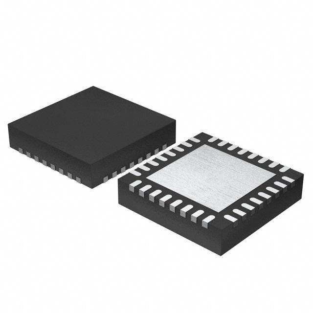
ICGOO电子元器件商城为您提供TLV320DAC3100IRHBR由Texas Instruments设计生产,在icgoo商城现货销售,并且可以通过原厂、代理商等渠道进行代购。 TLV320DAC3100IRHBR价格参考。Texas InstrumentsTLV320DAC3100IRHBR封装/规格:数据采集 - ADCs/DAC - 专用型, DAC 24 b 192k I²C,串行 32-VQFN(5x5)。您可以下载TLV320DAC3100IRHBR参考资料、Datasheet数据手册功能说明书,资料中有TLV320DAC3100IRHBR 详细功能的应用电路图电压和使用方法及教程。
| 参数 | 数值 |
| 产品目录 | 集成电路 (IC) |
| 描述 | IC DAC STER/AUDIO D LP 32QFN |
| 产品分类 | |
| 品牌 | Texas Instruments |
| 数据手册 | |
| 产品图片 |
|
| 产品型号 | TLV320DAC3100IRHBR |
| rohs | 无铅 / 符合限制有害物质指令(RoHS)规范要求 |
| 产品系列 | - |
| 供应商器件封装 | 32-VQFN(5x5) |
| 其它名称 | 296-27216-1 |
| 分辨率(位) | 24 b |
| 包装 | 剪切带 (CT) |
| 安装类型 | 表面贴装 |
| 封装/外壳 | 32-VFQFN 裸露焊盘 |
| 工作温度 | -40°C ~ 85°C |
| 数据接口 | I²C, 串行 |
| 标准包装 | 1 |
| 电压-电源 | 1.8V, 3.3V |
| 电压源 | 模拟和数字 |
| 类型 | DAC |
| 采样率(每秒) | 192k |


- 商务部:美国ITC正式对集成电路等产品启动337调查
- 曝三星4nm工艺存在良率问题 高通将骁龙8 Gen1或转产台积电
- 太阳诱电将投资9.5亿元在常州建新厂生产MLCC 预计2023年完工
- 英特尔发布欧洲新工厂建设计划 深化IDM 2.0 战略
- 台积电先进制程称霸业界 有大客户加持明年业绩稳了
- 达到5530亿美元!SIA预计今年全球半导体销售额将创下新高
- 英特尔拟将自动驾驶子公司Mobileye上市 估值或超500亿美元
- 三星加码芯片和SET,合并消费电子和移动部门,撤换高东真等 CEO
- 三星电子宣布重大人事变动 还合并消费电子和移动部门
- 海关总署:前11个月进口集成电路产品价值2.52万亿元 增长14.8%


PDF Datasheet 数据手册内容提取
Product Order Technical Tools & Support & Folder Now Documents Software Community TLV320DAC3100 SLAS671C–FEBRUARY2010–REVISEDJANUARY2017 TLV320DAC3100 Low-Power Stereo Audio DAC With Audio Processing and Mono Class-D Speaker Amplifier 1 Device Overview 1.1 Features 1 • StereoAudioDACwith95-dBSNR Volume-ControlSettings • Supports8-kHzto192-kHzSampleRates • DigitalSine-WaveGeneratorforBeepsandKey Clicks(PRB_P25) • MonoClass-DBTLSpeakerDriver(2.5WInto4-Ω or1.6WInto8-Ω) • ProgrammablePLLforFlexibleClockGeneration • TwoSingle-EndedInputsWithMixingandOutput • I2S,Left-Justified,Right-Justified,DSP,andTDM LevelControl AudioInterfaces • StereoHeadphone/LineoutandMonoClass-D • I2CControlWithRegisterAuto-Increment SpeakerOutputsAvailable • FullPower-DownControl • MicrophoneBias • PowerSupplies: • HeadphoneDetection – Analog:2.7V–3.6V • 25Built-inDigitalAudioProcessingBlocks – DigitalCore:1.65V–1.95V (PRB_P1– PRB_P25)ProvidingBiquadandFIR – DigitalI/O:1.1V–3.6V Filters,DRC,and3-DStructures – Class-D:2.7V–5.5V(SPKVDD ≥ AVDD) • DigitalMixingCapability • 5-mm×5-mm32-VQFNPackage • PinControlorRegisterControlforDigital-Playback 1.2 Applications • PortableAudioDevices • eBooks • MobileInternetDevices 1.3 Description The TLV320DAC3100 device is a low-power, highly integrated, high-performance stereo audio DAC with 24-bit stereoplaybackanddigitalaudioprocessingblocks. The device integrates headphone drivers and speaker drivers. The mono speaker driver can drive loads down to 4 Ω. The TLV320DAC3100 device has a suite of built-in processing blocks for digital audio processing. The digitalaudiodataformatisprogrammabletoworkwithpopularaudiostandardprotocols(I2S,left/right-justified)in master, slave, DSP, and TDM modes. Bass boost, treble, or EQ can be supported by the programmable digital signal-processing block. An on-chip PLL provides the high-speed clock needed by the digital signal-processing block. The volume level can be controlled either by pin control or by register control. The audio functions are controlledusingtheI2Cserialbus. The TLV320DAC3100 device has a programmable digital sine-wave generator and is available in a 32-pin VQFN package. DeviceInformation(1) PARTNUMBER PACKAGE BODYSIZE(NOM) TLV320DAC3100 VQFN(32) 5.00mm×5.00mm (1) Forallavailablepackages,seetheorderableaddendumattheendofthedatasheet. 1 An IMPORTANT NOTICE at the end of this data sheet addresses availability, warranty, changes, use in safety-critical applications, intellectualpropertymattersandotherimportantdisclaimers.PRODUCTIONDATA.
TLV320DAC3100 SLAS671C–FEBRUARY2010–REVISEDJANUARY2017 www.ti.com 1.4 Functional Block Diagram AVSS AVDD HPVSS HPVDD SPKVSS SPKVSS SPKVDD SPKVDD P0/R116 7-Bit VOL/MICDET Vol ADC Left and Right Audio Output Stage Volume-Control Register Power Management P0/R117 P1/R33–R34 GPIO1 GPIO De-Pop SDA I2C and SCL Soft Start RC CLK AIN1 AIN2 Analog Mono Class-D Note: Normally, Attenuation Speaker Driver MCLK is PLLinput; 0 dB to–78 dB however, BCLK or and Mute 6 dB to 24 dB GPIO1 can also be P0/R63/D5–D4 (0.5-dB Steps) (6-dB Steps) PLLinput. LData Left DAC AIN1 P1/R38 P1/R42 SPKP R Data S SPKP MCLK PLL (L+R)/2 Data DAC SPKM P0/R64 SPKM Analog ClassA/B Attenuation Headphone/Lineout 0 dB to–78 dB Driver WCLK and Mute 0 dB to 9 dB DIN (0.5-dB Steps) (1-dB Steps) BCLK Serial P1/R36 P1/R40 Interface Proincegss- D2i4g itdaBl Vtool AIN2 HPL and Blocks Mute MIXER RESET Clocks P1/R35 Analog Class-A/B Attenuation Headphone/Lineout 0 dB to–78 dB Driver and Mute 0 dB to 9 dB P0/R63/D3–D2 (0.5-dB Steps) (1-dB Steps) Right DAC P1/R37 P1/R41 LData R Data S DAC HPR (L+R)/2 Data P0/R64 P0/R64–R66 P1/R46 2 V/2.5 V/AVDD MICBIAS IOVSS IOVDD DVSS DVDD Copyright © 2017,Texas Instruments Incorporated 2 DeviceOverview Copyright©2010–2017,TexasInstrumentsIncorporated SubmitDocumentationFeedback ProductFolderLinks:TLV320DAC3100
TLV320DAC3100 www.ti.com SLAS671C–FEBRUARY2010–REVISEDJANUARY2017 Table of Contents 1 DeviceOverview......................................... 1 6 DetailedDescription................................... 18 .............................................. ............................................ 1.1 Features 1 6.1 Overview 18 ........................................... ........................... 1.2 Applications 1 6.2 FunctionalBlockDiagram 19 ............................................ ................................. 1.3 Description 1 6.3 FeatureDescription 19 ............................ ........................................ 1.4 FunctionalBlockDiagram 2 6.4 RegisterMap 64 2 Revision History......................................... 3 7 ApplicationandImplementation.................... 96 3 PinConfigurationandFunctions..................... 5 7.1 ApplicationInformation.............................. 96 ......................................... .................................. 3.1 PinAttributes 5 7.2 TypicalApplication 96 4 Specifications ............................................ 7 8 PowerSupplyRecommendations.................. 99 4.1 AbsoluteMaximumRatings.......................... 7 9 Layout................................................... 100 .......................................... .................................. 4.2 ESDRatings 7 9.1 Layout Guidelines 100 ................ .................................... 4.3 RecommendedOperatingConditions 7 9.2 Layout Example 100 4.4 Thermal Information.................................. 8 10 DeviceandDocumentationSupport.............. 101 ............................. ..................................... 4.5 ElectricalCharacteristics 8 10.1 DeviceSupport 101 .......................... ............................. 4.6 PowerDissipationRatings 10 10.2 CommunityResources 102 4.7 I2S,LJF,andRJFTiminginMasterMode.......... 10 10.3 Trademarks........................................ 102 4.8 I2S,LJF,andRJFTiminginSlaveMode........... 10 10.4 ElectrostaticDischargeCaution................... 102 ........................ ............................................ 4.9 DSPTiminginMasterMode 10 10.5 Glossary 102 4.10 DSPTiminginSlaveMode......................... 11 11 MechanicalPackagingandOrderable 4.11 I2CInterfaceTiming................................. 11 Information............................................. 102 4.12 TypicalCharacteristics.............................. 14 11.1 PackagingInformation............................. 102 5 ParameterMeasurementInformation.............. 17 2 Revision History NOTE:Pagenumbersforpreviousrevisionsmaydifferfrompagenumbersinthecurrentversion. ChangesfromRevisionB(April2016)toRevisionC Page • Added:Page0/Register51(0x33):GPIO1In/OutPinControl.............................................................. 73 ChangesfromRevisionA(May2012)toRevisionB Page • AddedESDRatingstable,FeatureDescriptionsection,DeviceFunctionalModes,Applicationand Implementationsection,PowerSupplyRecommendationssection,Layoutsection,DeviceandDocumentation Supportsection,andMechanical,Packaging,andOrderableInformationsection........................................... 1 • AddedPower-SupplySequencesectiontotheFeatureDescriptionsection................................................ 19 • ChangedSection6.3.10.1.2diagramsforPRB_P2/5/8/10/13/15/18/21/24/25toreflectthattheDRC_HPFfilter cannotbebypassedwhentheDRCisturnedoff .............................................................................. 26 • Addedsequenceforinsertingabeepinthemiddleofanalready-playingsignalandnotetextfollowingscriptin theKey-ClickFunctionalityWithDigitalSine-WaveGenerator(PRB_P25)section........................................ 42 • ChangedPRB_RxtoPRB_PxinDACSetupsection.......................................................................... 48 • ChangedDOSRnoteinPage0/Register14byswitchingmultiplevalueforFilterTypeAandFilterTypeC........ 67 • ChangeddescriptioninPage0/Register14toremoveparametersforminiDSP......................................... 67 • DeletedreferencetoDig_Mic_IninPage0/Register54tableforbitsD2-D1............................................. 74 • ChangedvaluesinPage0/Register69(0x45):DRCControl2............................................................. 77 • ChangedPage0,Register70,bitD3-D0decayratevaluefor0000fromDR=1.5625e–3toDR=0.015625........ 77 • SwitchedD1andD0descriptionssothatD1isforSPandD0isforHPinPage1/Register30table................ 81 • ChangedPage1/Register40,D1toreserved................................................................................. 83 • ChangedPage1/Register41,D1toreserved................................................................................. 84 Copyright©2010–2017,TexasInstrumentsIncorporated RevisionHistory 3 SubmitDocumentationFeedback ProductFolderLinks:TLV320DAC3100
TLV320DAC3100 SLAS671C–FEBRUARY2010–REVISEDJANUARY2017 www.ti.com ChangesfromOriginal(February2010)toRevisionA Page • Changedregister36toregister35insectionSection6.3.9.2................................................................. 25 • DeletedAnalogVolumeControlforHeadphoneandSpeakerOutputs(forD7=0)tableandaddedtablenoteto D7=1table............................................................................................................................ 45 • AddedD6–D0totheRegisterValuecolumnheadingandchangedAnalogAttenuationtoAnalogGain............... 45 • Changedpage0topage1insectionSection6.3.10.12.1.................................................................... 46 • Added80MHz≤(PLL_CLKIN×J.D×R/P)≤110MHzand4≤R×J≤259underEquation7 ........................ 55 • Added80MHz≤(PLL_CLKIN×J.D×R/P)≤110MHzand4≤R×J≤259underEquation8 ........................ 55 • AddedTimersectionandimageafterPLLsection.............................................................................. 56 • ChangedthedevicenamefromTLV320DAC3101toTLV320DAC3100intheDigitalAudioInterfacesection ....... 56 • ChangedD0=1toReservedinPage1/Register33........................................................................... 82 • Removedextraneouscross-referencesfordeletedtable...................................................................... 83 • AddedtablenotefollowingPage1/Register40............................................................................... 83 • AddedtablenotetoPage1/Register41(0x29):HPRDriver................................................................ 84 4 RevisionHistory Copyright©2010–2017,TexasInstrumentsIncorporated SubmitDocumentationFeedback ProductFolderLinks:TLV320DAC3100
TLV320DAC3100 www.ti.com SLAS671C–FEBRUARY2010–REVISEDJANUARY2017 3 Pin Configuration and Functions RHB Package (Top View) D D S D D S V M P V V M S D K K K K K K S D P P P P P P V V S S S S S S D A 24 23 22 21 20 19 18 17 SPKVSS 25 16 AVSS SPKP 26 15 NC HPL 27 14 AIN2 HPVDD 28 13 AIN1 HPVSS 29 12 MICBIAS HPR 30 11 VOL/MICDET RESET 31 10 SCL GPIO1 32 9 SDA 1 2 3 4 5 6 7 8 S D D C N K K K VS VD VD N DI CL CL CL O O D W B M I I P0048-16 3.1 Pin Attributes PinFunctions PIN I/O DESCRIPTION NAME NO. AIN1 13 I AnaloginputNo.1routedtooutputmixer AIN2 14 I AnaloginputNo.2routedtooutputmixer AVDD 17 - Analogpowersupply AVSS 16 - Analogground BCLK 7 I/O Audioserialbitclock DIN 5 I Audioserialdatainput DVDD 3 - Digitalpower–digitalcore DVSS 18 - Digitalground GPIO1 32 I/O General-purposeinput/outputpinandmultifunctionpin HPL 27 O Left-channelheadphone/linedriveroutput HPR 30 O Right-channelheadphone/linedriveroutput HPVDD 28 - Headphone/linedriverandPLLpower HPVSS 29 - Headphone/linedriverandPLLground IOVDD 2 - Interfacepower IOVSS 1 - Interfaceground MCLK 8 I Externalmasterclock MICBIAS 12 - Microphonebiasvoltage NC 4,15 I Noconnection RESET 31 I Devicereset SCL 10 I/O I2Ccontrolbusclockinput SDA 9 I/O I2Ccontrol-busdatainput Copyright©2010–2017,TexasInstrumentsIncorporated PinConfigurationandFunctions 5 SubmitDocumentationFeedback ProductFolderLinks:TLV320DAC3100
TLV320DAC3100 SLAS671C–FEBRUARY2010–REVISEDJANUARY2017 www.ti.com PinFunctions(continued) PIN I/O DESCRIPTION NAME NO. SPKM 19,23 I/O Cass-Dspeakerdriverinvertingoutput SPKP 22,26 Class-Dspeakerdrivernoninvertingoutput SPKVDD 21,24 Class-Dspeakerdriverpowersupply SPKVSS 20,25 Class-Dspeakerdriverpower-supplyground Volumecontrolorheadphonedetection.Notethatmicrophonedetectionisalsoavailableon VOL/MICDET 11 I devicesthathaveanADC. WCLK 6 I/O Audioserialwordclock 6 PinConfigurationandFunctions Copyright©2010–2017,TexasInstrumentsIncorporated SubmitDocumentationFeedback ProductFolderLinks:TLV320DAC3100
TLV320DAC3100 www.ti.com SLAS671C–FEBRUARY2010–REVISEDJANUARY2017 4 Specifications 4.1 Absolute Maximum Ratings overoperatingfree-airtemperaturerange(unlessotherwisenoted) (1) MIN MAX UNIT AVDDtoAVSS –0.3 3.9 V DVDDtoDVSS –0.3 2.5 V HPVDDtoHPVSS –0.3 3.9 V SPKVDDtoSPKVSS –0.3 6 V IOVDDtoIOVSS –0.3 3.9 V Digitalinputvoltage IOVSS–0.3 IOVDD+0.3 V Analoginputvoltage AVSS–0.3 AVDD+0.3 V Operatingtemperature –40 85 °C Junctiontemperature(T Max) 105 °C J Storagetemperature,T –55 150 °C stg (1) StressesbeyondthoselistedunderAbsoluteMaximumRatingsmaycausepermanentdamagetothedevice.Thesearestressratings only,andfunctionaloperationofthedeviceattheseoranyotherconditionsbeyondthoseindicatedunderRecommendedOperating Conditionsisnotimplied.Exposuretoabsolute-maximum-ratedconditionsforextendedperiodsmayaffectdevicereliability. 4.2 ESD Ratings VALUE UNIT Electrostatic Human-bodymodel(HBM),perANSI/ESDA/JEDECJS-001(1) ±2000 V V (ESD) discharge Charged-devicemodel(CDM),perJEDECspecificationJESD22-C101(2) ±1000 (1) JEDECdocumentJEP155statesthat500-VHBMallowssafemanufacturingwithastandardESDcontrolprocess. (2) JEDECdocumentJEP157statesthat250-VCDMallowssafemanufacturingwithastandardESDcontrolprocess. 4.3 Recommended Operating Conditions overoperatingfree-airtemperaturerange(unlessotherwisenoted) MIN NOM MAX UNIT AVDD(1) ReferencedtoAVSS(2) 2.7 3.3 3.6 DVDD ReferencedtoDVSS(2) 1.65 1.8 1.95 V HPVDD Power-supplyvoltage ReferencedtoHPVSS(2) 2.7 3.3 3.6 SPKVDD(1) ReferencedtoSPKVSS(2) 2.7 5.5 IOVDD ReferencedtoIOVSS(2) 1.1 3.3 3.6 Resistanceappliedacrossclass-D Speakerimpedance 4 Ω ouputpins(BTL) Headphoneimpedance ACcoupledtoR 16 Ω L VI Analogaudiofull-scaleinputvoltage AVDD=3.3V,single-ended 0.707 V RMS Stereolineoutputloadimpedance ACcoupledtoR 10 kΩ L MCLK(3) Masterclockfrequency IOVDD=3.3V 50 MHz f SCLclockfrequency 400 kHz SCL T Operatingfree-airtemperature –40 85 °C A (1) Tominimizebattery-currentleakage,theSPKVDDvoltagelevelshouldnotbebelowtheAVDDvoltagelevel. (2) Allgroundsonboardaretiedtogether,sotheyshouldnotdifferinvoltagebymorethan0.2-Vmaximumforanycombinationofground signals.Byuseofawidetraceorgroundplane,ensurealow-impedanceconnectionbetweenHPVSSandDVSS. (3) Themaximuminputfrequencymustbe50MHzforanydigitalpinusedasageneral-purposeclock. Copyright©2010–2017,TexasInstrumentsIncorporated Specifications 7 SubmitDocumentationFeedback ProductFolderLinks:TLV320DAC3100
TLV320DAC3100 SLAS671C–FEBRUARY2010–REVISEDJANUARY2017 www.ti.com 4.4 Thermal Information TLV320DAC3100 THERMALMETRIC(1) RHB(VQFN) UNIT 32PINS R Junction-to-ambientthermalresistance 31.4 °C/W θJA R Junction-to-case(top)thermalresistance 21.9 °C/W θJC(top) R Junction-to-boardthermalresistance 5.6 °C/W θJB ψ Junction-to-topcharacterizationparameter 0.2 °C/W JT ψ Junction-to-boardcharacterizationparameter 5.6 °C/W JB R Junction-to-case(bottom)thermalresistance 0.9 °C/W θJC(bot) (1) Formoreinformationabouttraditionalandnewthermalmetrics,seetheSemiconductorandICPackageThermalMetricsapplication report.. 4.5 Electrical Characteristics At25°C,AVDD=HPVDD=IOVDD=3.3V,SPKVDD=3.6V,DVDD=1.8V,f (audio)=48kHz,CODEC_CLKIN=256× S f ,PLL=Off,VOL/MICDETpindisabled(unlessotherwisenoted) S PARAMETER TESTCONDITIONS MIN TYP MAX UNIT INTERNALOSCILLATOR-RC_CLK Oscillatorfrequency 8.2 MHz VOLUMECONTROLPIN(ADC);VOL/MICDETpinenabled VOL/MICDETpinconfiguredasvolumecontrol(page0/register116,bitD7=1and 0.5x Inputvoltagerange 0 V page0/register67,bitD7=0) AVDD Inputcapacitance 2 pF Volumecontrolsteps 128 Steps MICROPHONEBIAS Page1/register46,bitsD1–D0=10 2.25 2.5 2.75 Voltageoutput V Page1/register46,bitsD1–D0=01 2 At4-mAloadcurrent,page1/register46,bitsD1–D0=10(MICBIAS=2.5V) 5 Voltageregulation mV At4-mAloadcurrent,page1/register46,bitsD1–D0=01(MICBIAS=2V) 7 AUDIODAC DACHEADPHONEOUTPUT,AC-coupledload=16Ω(single-ended),drivergain=0dB,parasiticcapacitance=30pF Full-scaleoutputvoltage(0dB) Outputcommon-modesetting=1.65V 0.707 VRMS SNR Signal-to-noiseratio Measuredasidle-channelnoise,A-weighted(1)(2) 80 95 dB THD Totalharmonicdistortion 0-dBFSinput –85 –65 dB THD+N Totalharmonicdistortion+noise 0-dBFSinput –82 –60 dB Muteattenuation 87 dB PSRR Power-supplyrejectionratio(3) RippleonHPVDD(3.3V)=200mVp-pat1kHz –62 dB PO Maximumoutputpower RRLL==3126ΩΩ,,TTHHDD++NN==––6600ddBB 2600 mW (1) Ratioofoutputlevelwith1-kHzfull-scalesine-waveinput,totheoutputlevelwiththeinputsshort-circuited,measuredA-weightedovera 20-Hzto20-kHzbandwidthusinganaudioanalyzer. (2) Allperformancemeasurementsdonewith20-kHzlow-passfilterand,wherenoted,A-weightedfilter.Failuretousesuchafiltermay resultinhigherTHD+NandlowerSNRanddynamicrangereadingsthanshownintheElectricalCharacteristics.Thelow-passfilter removesout-of-bandnoise,which,althoughnotaudible,mayaffectdynamicspecificationvalues. (3) DACtoheadphone-outPSRRmeasurementiscalculatedasPSRR=20×log(∆V /∆V ). HPL HPVDD 8 Specifications Copyright©2010–2017,TexasInstrumentsIncorporated SubmitDocumentationFeedback ProductFolderLinks:TLV320DAC3100
TLV320DAC3100 www.ti.com SLAS671C–FEBRUARY2010–REVISEDJANUARY2017 Electrical Characteristics (continued) At25°C,AVDD=HPVDD=IOVDD=3.3V,SPKVDD=3.6V,DVDD=1.8V,f (audio)=48kHz,CODEC_CLKIN=256× S f ,PLL=Off,VOL/MICDETpindisabled(unlessotherwisenoted) S PARAMETER TESTCONDITIONS MIN TYP MAX UNIT DACLINEOUT(HPDriverinLineoutMode) SNR Signal-to-noiseratio Measuredasidle-channelnoise,A-weighted 95 dB THD Totalharmonicdistortion 0-dBFSinput,0-dBgain –86 dB THD+N Totalharmonicdistortion+noise 0-dBFSinput,0-dBgain –82 dB DACDIGITALINTERPOLATIONFILTERCHARACTERISTICS SeeSection6.3.10.1.4forDACinterpolationfiltercharacteristics. DACOutputtoClass-DSPEAKEROUTPUT;Load=4Ω(Differential),50pF SPKVDD=3.6V,BTLmeasurement,DACinput=0dBFS,CM=1.8V,class-Dgain 2.3 =6dB,THD=–16.5dB Outputvoltage SPKVDD=3.6V,BTLmeasurement,DACinput=–2dBFS,CM=1.8V,class-D VRMS 2.1 gain=6dB,THD=–20dB Output,common-mode SPKVDD=3.6V,BTLmeasurement,DACinput=mute,class-Dgain=6dB 1.8 V SPKVDD=3.6V,BTLmeasurement,class-Dgain=6dB,measuredasidle-channel SNR Signal-to-noiseratio noise,A-weighted(withrespecttofull-scaleoutputvalueof2.3VRMS)(1)(2) 88 dB SPKVDD=3.6V,BTLmeasurement,DACinput=–6dBFS,CM=1.8V,class-D THD Totalharmonicdistortion –65 dB gain=6dB SPKVDD=3.6V,BTLmeasurement,DACinput=–6dBFS,CM=1.8V,class-D THD+N Totalharmonicdistortion+noise –63 dB gain=6dB PSRR Power-supplyrejectionratio(4) SPKVDD=3.6V,BTLmeasurement,rippleonSPKVDD=200mVp-pat1kHz –44 dB Muteattenuation 110 dB SPKVDD=3.6V,BTLmeasurement,CM=1.8V,class-Dgain=18dB,THD=10% 1 W PO Maximumoutputpower SPKVDD=4.3V,BTLmeasurement,CM=1.8V,class-Dgain=18dB,THD=10% 1.5 W SPKVDD=5.5V,BTLmeasurement,CM=1.8V,class-Dgain=18dB,THD=10% 2.5 W DACOutputtoClass-DSpeakerOutput;Load=8Ω(Differential),50pF SPKVDD=3.6V,BTLmeasurement,DACinput=0dBFS,CM=1.8V,class-Dgain =6dB,THD=–16.5dB 2.2 VRMS Outputvoltage SPKVDD=3.6V,BTLmeasurement,DACinput=–2dBFS,CM=1.8V,class-D gain=6dB,THD=–20dB 2.1 VRMS Output,common-mode SPKVDD=3.6V,BTLmeasurement,DACinput=mute,class-Dgain=6dB 1.8 V SPKVDD=3.6V,BTLmeasurement,class-Dgain=6dB,measuredasidle-channel SNR Signal-to-noiseratio 87 dB noise,A-weighted(withrespecttofull-scaleoutputvalueof2.2VRMS) SPKVDD=3.6V,BTLmeasurement,DACinput=–6dBFS,CM=1.8V,class-D THD Totalharmonicdistortion –67 dB gain=6dB SPKVDD=3.6V,BTLmeasurement,DACinput=–6dBFS,CM=1.8V,class-D THD+N Totalharmonicdistortion+noise –66 dB gain=6dB PSRR Power-supplyrejectionratio(4) SPKVDD=3.6V,BTLmeasurement,rippleonSPKVDD=200mVp-pat1kHz –44 dB Muteattenuation 110 dB SPKVDD=3.6V,BTLmeasurement,CM=1.8V,class-Dgain=18dB,THD=10% 0.7 PO Maximumoutputpower SPKVDD=4.3V,BTLmeasurement,CM=1.8V,class-Dgain=18dB,THD=10% 1 W SPKVDD=5.5V,BTLmeasurement,CM=1.8V,class-Dgain=18dB,THD=10% 1.6 Output-stageleakagecurrentfordirect SPKVDD=4.3V,deviceispowereddown(power-up-resetcondition) 80 nA batteryconnection DACPOWERCONSUMPTION ForDACpowerconsumptionbasedontheselectedprocessingblock,seeSection6.3.8. DIGITALINPUT/OUTPUT Logicfamily CMOS 0.7× VIH IIH=5µA,IOVDD=1.6V IOVDD IIH=5µA,IOVDD=1.6V IOVDD 0.3× VIL LogicLevel IIL=5µA,IOVDD=1.6V –0.3 IOVDD V IIL=5µA,IOVDD=1.6V 0 0.8× VOH IOH=2TTLloads IOVDD 0.1× VOL IOL=2TTLloads IOVDD Capacitiveload 10 pF (4) DACtospeaker-outPSRRisadifferentialmeasurementcalculatedasPSRR=20×log(∆V /∆V ). SPK(P+M) SPKVDD Copyright©2010–2017,TexasInstrumentsIncorporated Specifications 9 SubmitDocumentationFeedback ProductFolderLinks:TLV320DAC3100
TLV320DAC3100 SLAS671C–FEBRUARY2010–REVISEDJANUARY2017 www.ti.com 4.6 Power Dissipation Ratings Thisdatawastakenusing2-oz.(0,071-mmthick)traceandcopperpadthatissolderedtoaJEDEChigh-K,standard4-layer 3-inch×3-inch(7,62-cm×7,62-cm)PCB. PowerRatingat25°C DeratingFactor PowerRatingat70°C PowerRatingat85°C 2.3W 28.57mW/°C 1W 0.6W 4.7 I2S, LJF, and RJF Timing in Master Mode Allspecificationsat25°C,DVDD=1.8V.Note:Alltimingspecificationsaremeasuredatcharacterizationbutnottestedat finaltest.SeeFigure4-1. IOVDD=1.1V IOVDD=3.3V PARAMETER UNIT MIN MAX MIN MAX t (WS) WCLKdelay 45 20 ns d t (DO-WS) WCLKtodelay(forLJFmodeonly) 45 20 ns d t (DO-BCLK) BCLKtodelay 45 20 ns d t(DI) DINsetup 8 6 ns s t (DI) DINhold 8 6 ns h t Risetime 25 10 ns r t Falltime 25 10 ns f 4.8 I2S, LJF, and RJF Timing in Slave Mode Allspecificationsat25°C,DVDD=1.8V.Note:Alltimingspecificationsaremeasuredatcharacterizationbutnottestedat finaltest.SeeFigure4-2. IOVDD=1.1V IOVDD=3.3V PARAMETER UNIT MIN MAX MIN MAX t (BCLK) BCLKhighperiod 35 35 ns H t (BCLK) BCLKlowperiod 35 35 ns L t(WS) WCLKsetup 8 6 ns s t (WS) WCLKhold 8 6 ns h t (DO-WS) WCLKtodelay(forLJFmodeonly) 45 20 ns d t (DO-BCLK) BCLKtodelay 45 20 ns d t(DI) DINsetup 8 6 ns s t (DI) DINhold 8 6 ns h t Risetime 4 4 ns r t Falltime 4 4 ns f 4.9 DSP Timing in Master Mode Allspecificationsat25°C,DVDD=1.8V.Note:Alltimingspecificationsaremeasuredatcharacterizationbutnottestedat finaltest.SeeFigure4-3. IOVDD=1.1V IOVDD=3.3V PARAMETER UNIT MIN MAX MIN MAX t (WS) WCLKdelay 45 20 ns d t (DO-BCLK) BCLKtodelay 45 20 ns d t(DI) DINsetup 8 8 ns s t (DI) DINhold 8 8 ns h t Risetime 25 10 ns r t Falltime 25 10 ns f 10 Specifications Copyright©2010–2017,TexasInstrumentsIncorporated SubmitDocumentationFeedback ProductFolderLinks:TLV320DAC3100
TLV320DAC3100 www.ti.com SLAS671C–FEBRUARY2010–REVISEDJANUARY2017 4.10 DSP Timing in Slave Mode Allspecificationsat25°C,DVDD=1.8V.Note:Alltimingspecificationsaremeasuredatcharacterizationbutnottestedat finaltest.SeeFigure4-4. IOVDD=1.1V IOVDD=3.3V PARAMETER UNIT MIN MAX MIN MAX t (BCLK) BCLKhighperiod 35 35 ns H t (BCLK) BCLKlowperiod 35 35 ns L t(WS) WCLKsetup 8 8 ns s t (WS) WCLKhold 8 8 ns h t (DO-BCLK) BCLKtodelay 45 20 ns d t(DI) DINsetup 8 8 ns s t (DI) DINhold 8 8 ns h t Risetime 4 4 ns r t Falltime 4 4 ns f 4.11 I2C Interface Timing Allspecificationsat25°C,DVDD=1.8V.Note:Alltimingspecificationsaremeasuredatcharacterization.SeeFigure4-5. StandardMode FastMode PARAMETER UNIT MIN TYP MAX MIN TYP MAX f SCLclockfrequency 0 100 0 400 kHz SCL Holdtime(repeated)STARTcondition.Afterthis t 4 0.8 μs HD;STA period,thefirstclockpulseisgenerated. t LOWperiodoftheSCLclock 4.7 1.3 μs LOW t HIGHperiodoftheSCLclock 4 0.6 μs HIGH t SetuptimeforarepeatedSTARTcondition 4.7 0.8 μs SU;STA t Dataholdtime:forI2Cbusdevices 0 3.45 0 0.9 μs HD;DAT t Dataset-uptime 250 100 ns SU;DAT t SDAandSCLrisetime 1000 20+0.1C 300 ns r b t SDAandSCLfalltime 300 20+0.1C 300 ns f b t Set-uptimeforSTOPcondition 4 0.8 μs SU;STO BusfreetimebetweenaSTOPandSTART t 4.7 1.3 μs BUF condition C Capacitiveloadforeachbusline 400 400 pF b Copyright©2010–2017,TexasInstrumentsIncorporated Specifications 11 SubmitDocumentationFeedback ProductFolderLinks:TLV320DAC3100
TLV320DAC3100 SLAS671C–FEBRUARY2010–REVISEDJANUARY2017 www.ti.com WCLK t(WS) t d r BCLK t(DO-WS) t(DO-BCLK) t d d f DOUT t(DI) t(DI) S h DIN T0145-08 Figure4-1.I2S/LJF/RJFTiminginMasterMode WCLK t(WS) t h r t (BCLK) t(WS) H S BCLK t(BCLK) t(DO-WS) L d t(DO-BCLK) t d f DOUT t(DI) t(DI) S h DIN T0145-09 Figure4-2.I2S/LJF/RJFTiminginSlaveMode 12 Specifications Copyright©2010–2017,TexasInstrumentsIncorporated SubmitDocumentationFeedback ProductFolderLinks:TLV320DAC3100
TLV320DAC3100 www.ti.com SLAS671C–FEBRUARY2010–REVISEDJANUARY2017 WCLK t(WS) t(WS) d d t f BCLK td(DO-BCLK) tr DOUT t(DI) t(DI) S h DIN T0146-07 Figure4-3.DSPTiminginMasterMode WCLK t(WS) t(WS) S S t(WS) t(WS) h h t(BCLK) t L f BCLK t (BCLK) t(DO-BCLK) t H d r DOUT t(DI) t(DI) S h DIN T0146-08 Figure4-4.DSPTiminginSlaveMode SDA t t t t BUF LOW HIGH HD;STA t t r f SCL tHD;STA tSU;DAT tSU;STO tHD;DAT tSU;STA STO STA STA STO T0295-02 Figure4-5.I2CInterfaceTimingDiagram Copyright©2010–2017,TexasInstrumentsIncorporated Specifications 13 SubmitDocumentationFeedback ProductFolderLinks:TLV320DAC3100
TLV320DAC3100 SLAS671C–FEBRUARY2010–REVISEDJANUARY2017 www.ti.com 4.12 Typical Characteristics 4.12.1 DAC Performance 0 0 AVDD = HPVDD = 3.3 V AVDD = HPVDD = 3.3 V −20 IOVDD = SPKVDD = 3.3 V −20 IOVDD = SPKVDD = 3.3 V DVDD = 1.8 V DVDD = 1.8 V −40 −40 FS −60 FS −60 B B d d − − e −80 e −80 d d u u mplit −100 mplit −100 A A −120 −120 −140 −140 −160 −160 0 5 10 15 20 0 5 10 15 20 f − Frequency − kHz f − Frequency − kHz G001 G002 Figure4-6.AmplitudevsFrequency Figure4-7.AmplitudevsFrequency FFT-DACtoLineOutput FFT-DACtoHeadphoneOutput TEXTADDEDFORSPACING TEXTADDEDFORSPACING 0 B HPVDD = 2.7 V d −10 − CM = 1.35 V e ois −20 N n + −30 onic Distortio −−5400 HCMPHCV MP=DV 1D=D. 6 1=D5. 5 3=V .V 33 VV arm −60 HPVDD = 3.6 V H CM = 1.8 V al −70 Tot +N − −80 IDOVVDDDD = = 1 3.8.3 V V HD −90 Gain = 9 dB T RL = 16 W −100 0.00 0.02 0.04 0.06 0.08 0.10 0.12 0.14 PO − Output Power − W G025 Figure4-8.TotalHarmonicDistortion+NoisevsOutputPower HeadphoneOutputPower 14 Specifications Copyright©2010–2017,TexasInstrumentsIncorporated SubmitDocumentationFeedback ProductFolderLinks:TLV320DAC3100
TLV320DAC3100 www.ti.com SLAS671C–FEBRUARY2010–REVISEDJANUARY2017 4.12.2 Class-D Speaker Driver Performance 0 0 B AVDD = HPVDD = 3.3 V B SPKVDD = 3.3 V d d Noise − −10 ISDOPVVKDDVDDD = D= 1 3=.8. 35 V .V5 V Noise − −10 n + −20 RL = 4 W n + −20 o o orti Driver Gain orti SPKVDD = 3.6 V Dist −30 = 24 dB Dist −30 SPKVDD = 4.3 V monic −40 Driver Gain monic −40 SPKVDD = 5.5 V ar = 18 dB Driver Gain ar H H Total −50 = 12 dB Total −50 AHVPDVDD D= =3 .33. 3V V − − IOVDD = 3.3 V +N −60 Driver Gain +N −60 DVDD = 1.8 V HD = 6 dB HD Driver Gain = 18 dB T T RL = 4 W −70 −70 0.0 0.5 1.0 1.5 2.0 2.5 3.0 3.5 4.0 0.0 0.5 1.0 1.5 2.0 2.5 3.0 3.5 4.0 PO − Output Power − W PO − Output Power − W G010 G011 Figure4-9.TotalHarmonicDistortion+NoisevsOutputPower Figure4-10.TotalHarmonicDistortion+NoisevsOutputPower MaxClass-DSpeaker-DriverOutputPower(R =4Ω) Class-DSpeaker-DriverOutputPower(R =4Ω) L L 0 0 B AVDD = HPVDD = 3.3 V B SPKVDD = 3.3 V d d Noise − −10 ISDOPVVKDDVDDD = D= 1 3=.8. 35 V .V5 V Noise − −10 on + −20 RL = 8 W on + −20 SPKVDD = 3.6 V orti Driver Gain orti Dist −30 = 18 dB Dist −30 SPKVDD = 4.3 V armonic −40 Dr=iv 2e4r GdBain Driver Gain armonic −40 SPKVDD = 5.5 V H H Total −50 = 12 dB Total −50 AHVPDVDD D= =3 .33. 3V V − − IOVDD = 3.3 V +N −60 Driver Gain +N −60 DVDD = 1.8 V HD = 6 dB HD Driver Gain = 18 dB T T RL = 8 W −70 −70 0.0 0.5 1.0 1.5 2.0 2.5 0.0 0.5 1.0 1.5 2.0 2.5 3.0 PO − Output Power − W PO − Output Power − W G012 G013 Figure4-11.TotalHarmonicDistortion+NoisevsOutputPower Figure4-12.TotalHarmonicDistortion+NoisevsOutputPower MaxClass-DSpeaker-DriverOutputPower(R =8Ω) Class-DSpeaker-DriverOutputPower(R =8Ω) L L Copyright©2010–2017,TexasInstrumentsIncorporated Specifications 15 SubmitDocumentationFeedback ProductFolderLinks:TLV320DAC3100
TLV320DAC3100 SLAS671C–FEBRUARY2010–REVISEDJANUARY2017 www.ti.com 4.12.3 Analog Bypass Performance H 0 0 AVDD = HPVDD = 3.3 V AVDD = HPVDD = 3.3 V −20 IOVDD = SPKVDD = 3.3 V −20 IOVDD = SPKVDD = 3.3 V DVDD = 1.8 V DVDD = 1.8 V −40 −40 FS −60 FS −60 B B d d − − e −80 e −80 d d u u mplit −100 mplit −100 A A −120 −120 −140 −140 −160 −160 0 5 10 15 20 0 5 10 15 20 f − Frequency − kHz f − Frequency − kHz G008 G009 Figure4-13.AmplitudevsFrequency Figure4-14.AmplitudevsFrequency FFT-Line-InBypasstoLineOutput FFT-Line-InBypasstoHeadphoneOutput 4.12.4 MICBIAS Performance H 3.5 3.0 Micbias = AVDD (3.3 V) 2.5 Micbias = 2.5 V V e − 2.0 ag Micbias = 2 V Volt 1.5 − V 1.0 0.5 0.0 0.0 0.5 1.0 1.5 2.0 2.5 3.0 3.5 4.0 I − Current − mA G016 Figure4-15.VoltagevsCurrent MICBIAS 16 Specifications Copyright©2010–2017,TexasInstrumentsIncorporated SubmitDocumentationFeedback ProductFolderLinks:TLV320DAC3100
TLV320DAC3100 www.ti.com SLAS671C–FEBRUARY2010–REVISEDJANUARY2017 5 Parameter Measurement Information AllparametersaremeasuredaccordingtotheconditionsdescribedinSection4. Copyright©2010–2017,TexasInstrumentsIncorporated ParameterMeasurementInformation 17 SubmitDocumentationFeedback ProductFolderLinks:TLV320DAC3100
TLV320DAC3100 SLAS671C–FEBRUARY2010–REVISEDJANUARY2017 www.ti.com 6 Detailed Description 6.1 Overview The TLV320DAC3100 device is a highly integrated stereo-audio DAC for portable computing, communication, and entertainment applications. A register-based architecture eases integration with microprocessor-based systems through standard serial-interface buses. This device supports the two-wire I2C bus interface which provides full register access. All peripheral functions are controlled through these registersandtheonboardstatemachines. TheTLV320DAC3100deviceconsistsofthefollowingblocks: • StereoAudioDAC • Dynamicrangecompressor(DRC) • Digitalsine-wavegeneratorforclicksandbeeps • Stereoheadphoneandlineoutamplifier • Pin-controlledorregister-controlledvolumelevel • Power-downde-popandpower-upsoftstart • Analoginputs • I2Ccontrolinterface • Power-downcontrolblock Following a toggle of the RESET pin or a software reset, the device operates in the default mode. The I2C interfaceisusedtowritetothecontrolregisterstoconfigurethedevice. The I2C address assigned to the TLV320DAC3100 device is 0011000. This device always operates in an I2C slave mode. All registers are 8-bit, and all writable registers have read-back capability. The device auto-increments to support sequential addressing and can be used with the I2C fast mode. When the device is reset, all appropriate registers are updated by the host processor to configure the device as neededbytheuser. 18 DetailedDescription Copyright©2010–2017,TexasInstrumentsIncorporated SubmitDocumentationFeedback ProductFolderLinks:TLV320DAC3100
TLV320DAC3100 www.ti.com SLAS671C–FEBRUARY2010–REVISEDJANUARY2017 6.2 Functional Block Diagram AVSS AVDD HPVSS HPVDD SPKVSS SPKVSS SPKVDD SPKVDD P0/R116 7-Bit VOL/MICDET Vol ADC Left and Right Audio Output Stage Volume-Control Register Power Management P0/R117 P1/R33–R34 GPIO1 GPIO De-Pop SDA I2C and SCL Soft Start RC CLK AIN1 AIN2 Analog Mono Class-D Note: Normally, Attenuation Speaker Driver MCLK is PLLinput; 0 dB to–78 dB however, BCLK or and Mute 6 dB to 24 dB GPIO1 can also be P0/R63/D5–D4 (0.5-dB Steps) (6-dB Steps) PLLinput. LData Left DAC AIN1 P1/R38 P1/R42 SPKP R Data S SPKP MCLK PLL (L+R)/2 Data DAC SPKM P0/R64 SPKM Analog ClassA/B Attenuation Headphone/Lineout 0 dB to–78 dB Driver WCLK and Mute 0 dB to 9 dB DIN (0.5-dB Steps) (1-dB Steps) BCLK Serial P1/R36 P1/R40 Interface Proincegss- D2i4g itdaBl Vtool AIN2 HPL and Blocks Mute MIXER RESET Clocks P1/R35 Analog Class-A/B Attenuation Headphone/Lineout 0 dB to–78 dB Driver and Mute 0 dB to 9 dB P0/R63/D3–D2 (0.5-dB Steps) (1-dB Steps) Right DAC P1/R37 P1/R41 LData R Data S DAC HPR (L+R)/2 Data P0/R64 P0/R64–R66 P1/R46 2 V/2.5 V/AVDD MICBIAS IOVSS IOVDD DVSS DVDD Copyright © 2017,Texas Instruments Incorporated 6.3 Feature Description 6.3.1 Power-Supply Sequence The TLV320DAC3100 requires multiple power supply rails for operation. All the power rails must be powered up for the device to operate at the fullest potention. The following is the recommended power-up sequencingforproperoperation: 1. PowerupSPKVDDandSPRVDD 2. PowerupIOVDD 3. PowerupDVDDshortlyafterIOVDD 4. PowerupAVDDandHPVDD Copyright©2010–2017,TexasInstrumentsIncorporated DetailedDescription 19 SubmitDocumentationFeedback ProductFolderLinks:TLV320DAC3100
TLV320DAC3100 SLAS671C–FEBRUARY2010–REVISEDJANUARY2017 www.ti.com Although not necessary, if the system requires, during shutdown, remove the power supplies in the reverseorderoftheabovesequence. 6.3.2 Reset The TLV320DAC3100 internal logic must be initialized to a known condition for proper device function. To initialize the device to its default operating condition, the hardware reset pin (RESET) must be pulled low for at least 10 ns. For this initialization to work, both the IOVDD and DVDD supplies must be powered up. TIrecommendsthatwhiletheDVDDsupplypowersup,the RESETpinispulledlow. The device can also be reset via software reset. Writing a 1 into page 0 / register 1, bit D0 resets the device. 6.3.3 Device Start-Up Lockout Times After the TLV320DAC3100 is initialized through hardware reset at power up or software reset, the internal memories are initialized to default values. This initialization takes place within 1 ms after pulling the RESET signal high. During this initialization phase, no register-read or register-write operation should be performed on DAC coefficient buffers. Also, no block within the codec should be powered up during the initializationphase. 6.3.4 PLL Start-Up Whenever the PLL is powered up, a start-up delay of approximately of 10 ms occurs after the power-up command of the PLL and before the clocks are available to the codec. This delay is to ensure stable operationofthePLLandclock-dividerlogic. 6.3.5 Power-Stage Reset The power-stage-only reset is used to reset the device after an overcurrent latching shutdown has occurred. Using this reset re-enables the output stage without resetting all of the registers in the device. Each of the four power stages has its own dedicated reset bit. The headphone power-stage reset is performed by setting page 1/ register 31, bit D7 for HPL and by setting page 1 / register 31, bit D6 for HPR. The speaker power-stage reset is performed by setting page 1 / register 32, bit D7 for SPKP and SPKM. 6.3.6 Software Power Down By default, all circuit blocks are powered down following a reset condition. Hardware power up of each circuit block can be controlled by writing to the appropriate control register. This approach allows the lowest power-supply current for the functionality required. However, when a block is powered down, all of theregistersettingsaremaintainedaslongaspowerisstillbeingappliedtothedevice. 6.3.7 Audio Analog I/O The TLV320DAC3100 has a stereo audio DAC. The device supports a wide range of analog interfaces to support different headsets and analog outputs. The TLV320DAC3100 has features to interface output drivers (8-Ω, 16-Ω, 32-Ω). A special circuit has also been included in the TLV320DAC3100 to insert a short key-click sound into the stereo audio output. The key-click sound is used to provide feedback to the user when a particular button is pressed or item is selected. The specific sound of the keyclick can be adjusted by varying several register bits that control its frequency, duration, and amplitude (see Section6.3.10.7). 20 DetailedDescription Copyright©2010–2017,TexasInstrumentsIncorporated SubmitDocumentationFeedback ProductFolderLinks:TLV320DAC3100
TLV320DAC3100 www.ti.com SLAS671C–FEBRUARY2010–REVISEDJANUARY2017 6.3.8 Digital Processing Low-Power Modes The TLV320DAC3100 device can be tuned to minimize power dissipation, to maximize performance, or to an operating point between the two extremes to best fit the application. The choice of processing blocks, PRB_P1 to PRB_P25 for stereo playback, also influences the power consumption. In fact, the numerous processing blocks have been implemented to offer a choice among configurations having a different balanceofpoweroptimizationandsignal-processingcapabilities. 6.3.8.1 DACPlaybackonHeadphones,Stereo,48kHz,DVDD=1.8V,AVDD=3.3V, HPVDD=3.3V DOSR=128,ProcessingBlock=PRB_P7(InterpolationFilterB) Powerconsumption=24.28mW Table6-1.PRB_P7AlternativeProcessingBlocks,24.28mW PROCESSINGBLOCK FILTER ESTIMATEDPOWERCHANGE(mW) PRB_P1 A 1.34 PRB_P2 A 2.86 PRB_P3 A 2.11 PRB_P8 B 1.18 PRB_P9 B 0.53 PRB_P10 B 1.89 PRB_P11 B 0.87 PRB_P23 A 1.48 PRB_P24 A 2.89 PRB_P25 A 3.23 DOSR=64,ProcessingBlock=PRB_P7(InterpolationFilterB) Powerconsumption=24.5mW Table6-2.PRB_P7AlternativeProcessingBlocks,24.5mW PROCESSINGBLOCK FILTER ESTIMATEDPOWERCHANGE(mW) PRB_P1 A 1.17 PRB_P2 A 2.62 PRB_P3 A 2 PRB_P8 B 0.99 PRB_P9 B 0.5 PRB_P10 B 1.46 PRB_P11 B 0.66 PRB_P23 A 1.43 PRB_P24 A 2.69 PRB_P25 A 2.92 6.3.8.2 DACPlaybackonHeadphones,Mono,48kHz,DVDD=1.8V,AVDD=3.3V, HPVDD=3.3V DOSR=128,ProcessingBlock=PRB_P12(InterpolationFilterB) Powerconsumption=15.4mW Table6-3.PRB_P12AlternativeProcessingBlocks,15.4mW PROCESSINGBLOCK FILTER ESTIMATEDPOWERCHANGE(mW) PRB_P4 A 0.57 Copyright©2010–2017,TexasInstrumentsIncorporated DetailedDescription 21 SubmitDocumentationFeedback ProductFolderLinks:TLV320DAC3100
TLV320DAC3100 SLAS671C–FEBRUARY2010–REVISEDJANUARY2017 www.ti.com Table6-3.PRB_P12AlternativeProcessingBlocks,15.4mW(continued) PROCESSINGBLOCK FILTER ESTIMATEDPOWERCHANGE(mW) PRB_P5 A 1.48 PRB_P6 A 1.08 PRB_P13 B 0.56 PRB_P14 B 0.27 PRB_P15 B 0.89 PRB_P16 B 0.31 DOSR=64,ProcessingBlock=PRB_P12(InterpolationFilterB) Powerconsumption=15.54mW Table6-4.PRB_P12AlternativeProcessingBlocks,15.54mW PROCESSINGBLOCK FILTER ESTIMATEDPOWERCHANGE(mW) PRB_P4 A 0.37 PRB_P5 A 1.23 PRB_P6 A 1.15 PRB_P13 B 0.43 PRB_P14 B 0.13 PRB_P15 B 0.85 PRB_P16 B 0.21 6.3.8.3 DACPlaybackonHeadphones,Stereo,8kHz,DVDD=1.8V,AVDD=3.3V, HPVDD=3.3V DOSR=768,ProcessingBlock=PRB_P7(InterpolationFilterB) Powerconsumption=22.44mW Table6-5.PRB_P7AlternativeProcessingBlocks,22.44mW PROCESSINGBLOCK FILTER ESTIMATEDPOWERCHANGE(mW) PRB_P1 A 0.02 PRB_P2 A 0.31 PRB_P3 A 0.23 PRB_P8 B 0.28 PRB_P9 B –0.03 PRB_P10 B 0.14 PRB_P11 B 0.05 PRB_P23 A 0.29 PRB_P24 A 0.26 PRB_P25 A 0.47 DOSR=384,ProcessingBlock=PRB_P7(InterpolationFilterB) Powerconsumption=22.83mW Table6-6.PRB_P7AlternativeProcessingBlocks,22.83mW PROCESSINGBLOCK FILTER ESTIMATEDPOWERCHANGE(mW) PRB_P1 A 0.27 PRB_P2 A 0.4 PRB_P3 A 0.34 PRB_P8 B 0.2 22 DetailedDescription Copyright©2010–2017,TexasInstrumentsIncorporated SubmitDocumentationFeedback ProductFolderLinks:TLV320DAC3100
TLV320DAC3100 www.ti.com SLAS671C–FEBRUARY2010–REVISEDJANUARY2017 Table6-6.PRB_P7AlternativeProcessingBlocks,22.83mW(continued) PROCESSINGBLOCK FILTER ESTIMATEDPOWERCHANGE(mW) PRB_P9 B 0.08 PRB_P10 B 0.24 PRB_P11 B 0.12 PRB_P23 A 0.23 PRB_P24 A 0.42 PRB_P25 A 0.46 6.3.8.4 DACPlaybackonHeadphones,Mono,8kHz,DVDD=1.8V,AVDD=3.3V, HPVDD=3.3V DOSR=768,ProcessingBlock=PRB_P12(InterpolationFilterB) Powerconsumption=14.49mW Table6-7.PRB_P12AlternativeProcessingBlocks,14.49mW PROCESSINGBLOCK FILTER ESTIMATEDPOWERCHANGE(mW) PRB_P4 A –0.04 PRB_P5 A 0.2 PRB_P6 A –0.01 PRB_P13 B 0.1 PRB_P14 B 0.05 PRB_P15 B –0.03 PRB_P16 B 0.07 DOSR=384,ProcessingBlock=PRB_P12(InterpolationFilterB) Powerconsumption=14.42mW Table6-8.PRB_P12AlternativeProcessingBlocks,14.42mW PROCESSINGBLOCK FILTER ESTIMATEDPOWERCHANGE(mW) PRB_P4 A 0.16 PRB_P5 A 0.3 PRB_P6 A 0.2 PRB_P13 B 0.15 PRB_P14 B 0.07 PRB_P15 B 0.18 PRB_P16 B 0.09 Copyright©2010–2017,TexasInstrumentsIncorporated DetailedDescription 23 SubmitDocumentationFeedback ProductFolderLinks:TLV320DAC3100
TLV320DAC3100 SLAS671C–FEBRUARY2010–REVISEDJANUARY2017 www.ti.com 6.3.8.5 DACPlaybackonHeadphones,Stereo,192kHz,DVDD=1.8V,AVDD=3.3V, HPVDD=3.3V DOSR=32,ProcessingBlock=PRB_P17(InterpolationFilterC) Powerconsumption=27.05mW Table6-9.PRB_P17AlternativeProcessingBlocks,27.05mW PROCESSINGBLOCK FILTER ESTIMATEDPOWERCHANGE(mW) PRB_P18 C 5.28 PRB_P19 C 1.98 6.3.8.6 DACPlaybackonLineOut(10k-Ω load),Stereo,48kHz,DVDD=1.8V,AVDD=3V, HPVDD=3V DOSR=64,ProcessingBlock=PRB_P7(InterpolationFilterB) Powerconsumption=12.85mW 6.3.9 Analog Signals TheTLV320DAC3100analogsignalsconsistof: • Microphonebias(MICBIAS) • AnaloginputsAIN1andAIN2 • Analog outputs, class-D speaker driver and headphone and lineout driver, providing output capability fortheDAC,AIN1,AIN2oramixofthethree 6.3.9.1 MICBIAS The TLV320DAC3100 device includes a microphone bias circuit that sources up to 4 mA of current and is programmabletoa2-V,2.5-V,orAVDDlevel.Theleveliscontrolledbywritingtopage1/register46,bits D1–D0.Table6-10liststhisfunctionality. Table6-10.MICBIASSettings D1 D0 FUNCTIONALITY 0 0 MICBIASoutputispowereddown 0 1 MICBIASoutputispoweredto2V 1 0 MICBIASoutputispoweredto2.5V 1 1 MICBIASoutputispoweredtoAVDD During normal operation, MICBIAS can be set to 2.5 V for better performance. However, based on the model of the selected microphone, optimal performance can be obtained at another setting and therefore theperformanceatagivensettingmustbeverified. The lowest current consumption occurs when MICBIAS is powered down. The next-lowest current consumption occurs when MICBIAS is set at AVDD. The highest current consumption occurs when MICBIASissetat2V. 6.3.9.2 AnalogInputsAIN1andAIN2 AIN1 (pin 13) and AIN2 (pin 14) are inputs to the output mixer along with the DAC output. Page 1 / register35providescontrolsignalsfordeterminingthesignalsroutedthroughtheoutputmixer.Theoutput of the output mixer then can be attenuated or gained through the class-D and, or, headphone and lineout drivers. 24 DetailedDescription Copyright©2010–2017,TexasInstrumentsIncorporated SubmitDocumentationFeedback ProductFolderLinks:TLV320DAC3100
TLV320DAC3100 www.ti.com SLAS671C–FEBRUARY2010–REVISEDJANUARY2017 6.3.10 Audio DAC and Audio Analog Outputs Each channel of the stereo audio DAC consists of a digital-audio processing block, a digital interpolation filter, a digital delta-sigma modulator, and an analog reconstruction filter. The DAC oversampling ratio (typically DOSR is between 32 and 128) exhibits good dynamic range by ensuring that the quantization noisegeneratedwithinthedelta-sigmamodulatorstaysoutsideoftheaudiofrequencyband.Audioanalog outputsincludestereoheadphone,orlineouts,andstereoclass-Dspeakeroutputs. 6.3.10.1 DAC The TLV320DAC3100 stereo-audio DAC supports data rates from 8 kHz to 192 kHz. Each channel of the stereo audio-DAC consists of a signal-processing engine with fixed processing blocks, a digital interpolation filter, a multibit digital delta-sigma modulator, and an analog reconstruction filter. The DAC is designed to provide enhanced performance at low sampling rates through increased oversampling and image filtering, thereby keeping quantization noise generated within the delta-sigma modulator and signal images strongly suppressed within the audio band to beyond 20 kHz. To handle multiple input rates and optimize power dissipation and performance, the TLV320DAC3100 device allows the system designer to program the oversampling rates over a wide range from 1 to 1024 by configuring page 0 / register 13 and page 0 / register 14. The system designer can choose higher oversampling ratios for lower input data ratesandloweroversamplingratiosforhigherinputdatarates. The TLV320DAC3100 DAC channel includes a built-in digital interpolation filter to generate oversampled data for the delta-sigma modulator. The interpolation filter can be chosen from three different types, dependingonrequiredfrequencyresponse,groupdelay,andsamplingrate. DAC power up is controlled by writing to page 0 / register 63, bit D7 for the left channel and bit D6 for the right channel. The left-channel DAC clipping flag is provided as a read-only bit on page 0 / register 39, bit D7.Theright-channelDACclippingflagisprovidedasaread-onlybitonpage0/register39,bitD6. 6.3.10.1.1 DACProcessingBlocks The TLV320DAC3100 device implements signal-processing capabilities and interpolation filtering through processing blocks. These fixed processing blocks give users the choice of how much and what type of signalprocessingtheyuseandwhichinterpolationfilterisapplied. The choices among these processing blocks allow the system designer to balance power conservation and signal-processing flexibility. Table 6-11 gives an overview of all available processing blocks of the DAC channel and their properties. The resource-class column gives an approximate indication of power consumptionforthedigital(DVDD)supply;however,basedontheout-of-bandnoisespectrum,theanalog powerconsumptionofthedrivers(HPVDD)maydiffer. Thesignalprocessingblocksavailableare: • First-orderIIR • Scalablenumberofbiquadfilters • 3Deffect • Digitalsine-wave(beep)generator The processing blocks are tuned for common cases and can achieve high image rejection or low group delay in combination with various signal-processing effects such as audio effects and frequency shaping. Theavailablefirst-orderIIRandbiquadfiltershavefullyuser-programmablecoefficients. Table6-11.Overview– DACPredefinedProcessingBlocks PROCESSING INTERPOLATION FIRST-ORDER NUMBEROF BEEP RESOURCE CHANNEL DRC 3D BLOCKNO. FILTER IIRAVAILABLE BIQUADS GENERATOR CLASS PRB_P1 A Stereo No 3 No No No 8 PRB_P2 A Stereo Yes 6 Yes No No 12 PRB_P3 A Stereo Yes 6 No No No 10 PRB_P4 A Left No 3 No No No 4 Copyright©2010–2017,TexasInstrumentsIncorporated DetailedDescription 25 SubmitDocumentationFeedback ProductFolderLinks:TLV320DAC3100
TLV320DAC3100 SLAS671C–FEBRUARY2010–REVISEDJANUARY2017 www.ti.com Table6-11.Overview– DACPredefinedProcessingBlocks (continued) PROCESSING INTERPOLATION FIRST-ORDER NUMBEROF BEEP RESOURCE CHANNEL DRC 3D BLOCKNO. FILTER IIRAVAILABLE BIQUADS GENERATOR CLASS PRB_P5 A Left Yes 6 Yes No No 6 PRB_P6 A Left Yes 6 No No No 6 PRB_P7 B Stereo Yes 0 No No No 6 PRB_P8 B Stereo No 4 Yes No No 8 PRB_P9 B Stereo No 4 No No No 8 PRB_P10 B Stereo Yes 6 Yes No No 10 PRB_P11 B Stereo Yes 6 No No No 8 PRB_P12 B Left Yes 0 No No No 3 PRB_P13 B Left No 4 Yes No No 4 PRB_P14 B Left No 4 No No No 4 PRB_P15 B Left Yes 6 Yes No No 6 PRB_P16 B Left Yes 6 No No No 4 PRB_P17 C Stereo Yes 0 No No No 3 PRB_P18 C Stereo Yes 4 Yes No No 6 PRB_P19 C Stereo Yes 4 No No No 4 PRB_P20 C Left Yes 0 No No No 2 PRB_P21 C Left Yes 4 Yes No No 3 PRB_P22 C Left Yes 4 No No No 2 PRB_P23 A Stereo No 2 No Yes No 8 PRB_P24 A Stereo Yes 5 Yes Yes No 12 PRB_P25 A Stereo Yes 5 Yes Yes Yes 12 6.3.10.1.2 DACProcessingBlocks—Details 6.3.10.1.2.1 ThreeBiquads,FilterA ´ BiQuad BiQuad BiQuad Interp. to A B C FilterA from Modulator Interface Digital Volume Ctrl Figure6-1.SignalChainfor PRB_P1andPRB_P4 6.3.10.1.2.2 SixBiquads,First-OrderIIR,DRC,FilterAorB (cid:1)(cid:2)(cid:3)(cid:4)(cid:5)(cid:6)(cid:7) (cid:1)(cid:1)(cid:17) (cid:14)(cid:9)(cid:21)(cid:22)(cid:23)(cid:24) (cid:14)(cid:9)(cid:21)(cid:22)(cid:23)(cid:24) (cid:14)(cid:9)(cid:21)(cid:22)(cid:23)(cid:24) (cid:14)(cid:9)(cid:21)(cid:22)(cid:23)(cid:24) (cid:14)(cid:9)(cid:21)(cid:22)(cid:23)(cid:24) (cid:14)(cid:9)(cid:21)(cid:22)(cid:23)(cid:24) (cid:19)(cid:20)(cid:8) (cid:8)(cid:9)(cid:10)(cid:3)(cid:4)(cid:5)(cid:11) (cid:15) (cid:3)(cid:13) (cid:12) (cid:14) (cid:18) (cid:16) (cid:25) (cid:8) (cid:29)(cid:5)(cid:13)(cid:26)(cid:11) (cid:12)(cid:11)(cid:13)(cid:5)(cid:11)(cid:14) (cid:26)(cid:13)(cid:24)(cid:22)(cid:10)(cid:23)(cid:3)(cid:13)(cid:5) (cid:9)(cid:2)(cid:3)(cid:4)(cid:5)(cid:29)(cid:23)(cid:30)(cid:4) (cid:16)(cid:9)(cid:27)(cid:9)(cid:3)(cid:23)(cid:10) (cid:28)(cid:13)(cid:10)(cid:22)(cid:26)(cid:4) (cid:16)(cid:17)(cid:18) (cid:18)(cid:3)(cid:5)(cid:10) Figure6-2.SignalChainfor PRB_P2,PRB_P5,PRB_P10, andPRB_P15 26 DetailedDescription Copyright©2010–2017,TexasInstrumentsIncorporated SubmitDocumentationFeedback ProductFolderLinks:TLV320DAC3100
TLV320DAC3100 www.ti.com SLAS671C–FEBRUARY2010–REVISEDJANUARY2017 6.3.10.1.2.3 SixBiquads,First-OrderIIR,FilterAorB Interp. ´ IIR BiQuad BiQuad BiQuad BiQuad BiQuad BiQuad Filter to A B C D E F Modulator from A,B Interface Digital Volume Ctrl Figure6-3.SignalChainfor PRB_P3,PRB_P6,PRB_P11, andPRB_P16 6.3.10.1.2.4 IIR,FilterBorC Interp. ´ IIR Filter to Modulator from B,C Interface Digital Volume Ctrl Figure6-4.SignalChainfor PRB_P7,PRB_P12,PRB_P17, andPRB_P20 6.3.10.1.2.5 FourBiquads,DRC,FilterB (cid:12)(cid:9)(cid:26)(cid:22)(cid:23)(cid:21) (cid:12)(cid:9)(cid:26)(cid:22)(cid:23)(cid:21) (cid:12)(cid:9)(cid:26)(cid:22)(cid:23)(cid:21) (cid:12)(cid:9)(cid:26)(cid:22)(cid:23)(cid:21) (cid:1)(cid:2)(cid:3)(cid:4)(cid:5)(cid:6)(cid:7) (cid:13) (cid:17)(cid:18)(cid:8) (cid:3)(cid:19) (cid:27) (cid:12) (cid:16) (cid:14) (cid:8)(cid:9)(cid:10)(cid:3)(cid:4)(cid:5)(cid:11)(cid:12) (cid:28)(cid:5)(cid:19)(cid:20)(cid:11) (cid:20)(cid:19)(cid:21)(cid:22)(cid:10)(cid:23)(cid:3)(cid:19)(cid:5) (cid:9)(cid:2)(cid:3)(cid:4)(cid:5)(cid:28)(cid:23)(cid:29)(cid:4) (cid:14)(cid:9)(cid:24)(cid:9)(cid:3)(cid:23)(cid:10) (cid:25)(cid:19)(cid:10)(cid:22)(cid:20)(cid:4) (cid:14)(cid:15)(cid:16) (cid:16)(cid:3)(cid:5)(cid:10) Figure6-5.SignalChainfor PRB_P8andPRB_P13 6.3.10.1.2.6 FourBiquads,FilterB ´ BiQuad BiQuad BiQuad BiQuad Interp. to A B C D Filter B Modulator from Interface Digital Volume Ctrl Figure6-6.SignalChainfor PRB_P9andPRB_P14 6.3.10.1.2.7 FourBiquads,First-OrderIIR,DRC,FilterC (cid:1)(cid:1)(cid:15) (cid:25)(cid:9)(cid:26)(cid:21)(cid:22)(cid:20) (cid:25)(cid:9)(cid:26)(cid:21)(cid:22)(cid:20) (cid:25)(cid:9)(cid:26)(cid:21)(cid:22)(cid:20) (cid:25)(cid:9)(cid:26)(cid:21)(cid:22)(cid:20) (cid:16)(cid:17)(cid:8) (cid:1)(cid:2)(cid:3)(cid:4)(cid:5)(cid:6)(cid:7) (cid:13) (cid:3)(cid:18) (cid:27) (cid:25) (cid:12) (cid:14) (cid:8)(cid:9)(cid:10)(cid:3)(cid:4)(cid:5)(cid:11)(cid:12) (cid:19)(cid:18)(cid:20)(cid:21)(cid:10)(cid:22)(cid:3)(cid:18)(cid:5) (cid:28)(cid:5)(cid:18)(cid:19)(cid:11) (cid:9)(cid:2)(cid:3)(cid:4)(cid:5)(cid:28)(cid:22)(cid:29)(cid:4) (cid:14)(cid:9)(cid:23)(cid:9)(cid:3)(cid:22)(cid:10) (cid:24)(cid:18)(cid:10)(cid:21)(cid:19)(cid:4) (cid:14)(cid:15)(cid:12) (cid:12)(cid:3)(cid:5)(cid:10) Figure6-7.SignalChainfor PRB_P18andPRB_P21 Copyright©2010–2017,TexasInstrumentsIncorporated DetailedDescription 27 SubmitDocumentationFeedback ProductFolderLinks:TLV320DAC3100
TLV320DAC3100 SLAS671C–FEBRUARY2010–REVISEDJANUARY2017 www.ti.com 6.3.10.1.2.8 FourBiquads,First-OrderIIR,FilterC ´ BiQuad BiQuad BiQuad BiQuad Interp. IIR to A B C D Filter C modulator from Interface Digital Volume Ctrl Figure6-8.SignalChainfor PRB_P19andPRB_P22 6.3.10.1.2.9 TwoBiquads,3D,FilterA From + ChaLnenfet-l + BiqBuLad BiqCuLad FIniltteerrpA. ´ ModulatToor Interface + Digital Volume Ctrl + + Biquad Biquad 3D – AL AR PGA + From – ChRaingnhet-l + BiqBuRad BiqCuRad FIniltteerrpA. ´ ModulatToor Interface Digital Volume Ctrl NOTE: A meansbiquadAoftheleftchannel,andsimilarly,B meansbiquadBoftherightchannel. L R Figure6-9.SignalChainforPRB_P23 28 DetailedDescription Copyright©2010–2017,TexasInstrumentsIncorporated SubmitDocumentationFeedback ProductFolderLinks:TLV320DAC3100
TLV320DAC3100 www.ti.com SLAS671C–FEBRUARY2010–REVISEDJANUARY2017 6.3.10.1.2.10 FiveBiquads,DRC,3D,FilterA (cid:24)(cid:13) !(cid:18) (cid:17)(cid:9)(cid:12)(cid:9)(cid:21)(cid:24)(cid:11) (cid:28) (cid:28) (cid:1)(cid:2)(cid:3)(cid:1)(cid:4)(cid:8)(cid:5)(cid:6) (cid:1)(cid:2)(cid:3)(cid:22)(cid:4)(cid:8)(cid:5)(cid:6) (cid:1)(cid:2)(cid:3)(cid:20)(cid:4)(cid:8)(cid:5)(cid:6) (cid:1)(cid:2)(cid:3)(cid:23)(cid:4)(cid:8)(cid:5)(cid:6) (cid:1)(cid:2)(cid:3)(cid:16)(cid:4)(cid:8)(cid:5)(cid:6) $(cid:26)(cid:16) (cid:16)(cid:9)(cid:10)(cid:2)(cid:17)(cid:11)(cid:11)(cid:12)(cid:12)(cid:13)(cid:13)(cid:14)(cid:18)(cid:7)(cid:15) (cid:19) ! (cid:6)(cid:4)(cid:17)(cid:5)(cid:11) (cid:11) (cid:13) (cid:17)(cid:12)(cid:24)(cid:11) (cid:28) "(cid:30)(cid:5)(cid:10)(cid:10)(cid:12)(cid:17) (cid:2)(cid:10)(cid:11)(cid:12)(cid:13)(cid:24)(cid:5)"(cid:12) (cid:20)(cid:2)(cid:29)(cid:2)(cid:11)(cid:5)(cid:17) # (cid:17)(cid:4)!(cid:12) (cid:20)(cid:21)(cid:22) (cid:22)(cid:11)(cid:13)(cid:17) (cid:28) (cid:28) (cid:1)(cid:2)(cid:3)(cid:4)(cid:5)(cid:6) (cid:1)(cid:2)(cid:3)(cid:4)(cid:5)(cid:6) (cid:25)(cid:20) (cid:31) (cid:7)(cid:8) (cid:7)(cid:21) (cid:26)(cid:27)(cid:7) (cid:31) (cid:24)(cid:13) !(cid:18) (cid:13)(cid:9)(cid:2)(cid:29)(cid:9)(cid:21)(cid:30)(cid:11) (cid:28) (cid:28) (cid:1)(cid:2)(cid:3)(cid:1)(cid:4)(cid:21)(cid:5)(cid:6) (cid:1)(cid:2)(cid:3)(cid:22)(cid:4)(cid:21)(cid:5)(cid:6) (cid:1)(cid:2)(cid:3)(cid:20)(cid:4)(cid:21)(cid:5)(cid:6) (cid:1)(cid:2)(cid:3)(cid:23)(cid:4)(cid:21)(cid:5)(cid:6) (cid:1)(cid:2)(cid:3)(cid:16)(cid:4)(cid:21)(cid:5)(cid:6) $(cid:26)(cid:16) (cid:16)(cid:9)(cid:10)(cid:2)(cid:17)(cid:11)(cid:11)(cid:12)(cid:12)(cid:13)(cid:13)(cid:14)(cid:18)(cid:7)(cid:15) (cid:19) ! (cid:6)(cid:4)(cid:17)(cid:5)(cid:11) (cid:11) (cid:13) (cid:13)(cid:2)(cid:29)(cid:30)(cid:11) "(cid:30)(cid:5)(cid:10)(cid:10)(cid:12)(cid:17) (cid:2)(cid:10)(cid:11)(cid:12)(cid:13)(cid:24)(cid:5)"(cid:12) (cid:20)(cid:2)(cid:29)(cid:2)(cid:11)(cid:5)(cid:17) # (cid:17)(cid:4)!(cid:12) (cid:20)(cid:21)(cid:22) (cid:22)(cid:11)(cid:13)(cid:17) Figure6-10.SignalChainforPRB_P24 6.3.10.1.2.11 FiveBiquads,DRC,3D,BeepGenerator,FilterA (cid:27)(cid:13)!"(cid:18) (cid:17)(cid:9)(cid:12)(cid:9)(cid:22)(cid:27)(cid:11) (cid:20) (cid:20) (cid:1)(cid:2)(cid:3)(cid:1)(cid:4)(cid:8)(cid:5)(cid:6) (cid:1)(cid:2)(cid:3)(cid:23)(cid:4)(cid:8)(cid:5)(cid:6) (cid:1)(cid:2)(cid:3)(cid:21)(cid:4)(cid:8)(cid:5)(cid:6) (cid:1)(cid:2)(cid:3)(cid:26)(cid:4)(cid:8)(cid:5)(cid:6) (cid:1)(cid:2)(cid:3)(cid:16)(cid:4)(cid:8)(cid:5)(cid:6) (cid:24)(cid:25)(cid:16) (cid:16)(cid:9)(cid:10)(cid:2)(cid:17)(cid:11)(cid:11)(cid:12)(cid:12)(cid:13)(cid:13)(cid:14)(cid:18)(cid:7)(cid:15) (cid:19) (cid:20)"!(cid:6)(cid:4)(cid:17)(cid:5)(cid:11)!(cid:11)!(cid:13) (cid:17)(cid:12)(cid:27)(cid:11) (cid:20) #(cid:31)(cid:5)(cid:10)(cid:10)(cid:12)(cid:17) (cid:2)(cid:10)(cid:11)(cid:12)(cid:13)(cid:27)(cid:5)#(cid:12) (cid:21)(cid:22)(cid:23) (cid:21)(cid:2)(cid:30)(cid:2)(cid:11)(cid:5)(cid:17) $!(cid:17)(cid:4)"(cid:12) (cid:20) (cid:20) (cid:1)(cid:2)(cid:3)(cid:4)(cid:5)(cid:6) (cid:1)(cid:2)(cid:3)(cid:4)(cid:5)(cid:6) (cid:28)(cid:21) (cid:23)(cid:11)(cid:13)(cid:17) (cid:7) (cid:7) (cid:25)(cid:29)(cid:7) (cid:8) (cid:22) (cid:19) (cid:1)(cid:12)(cid:12)(cid:14) (cid:1)(cid:12)(cid:12)(cid:14) $!(cid:17)(cid:4)"(cid:12) (cid:29)(cid:12)(cid:10)(cid:15) (cid:23)(cid:11)(cid:13)(cid:17) (cid:19) (cid:27)(cid:13)!"(cid:18) (cid:13)(cid:9)(cid:2)(cid:30)(cid:9)(cid:22)(cid:31)(cid:11) (cid:20) (cid:20) (cid:1)(cid:2)(cid:3)(cid:1)(cid:4)(cid:22)(cid:5)(cid:6) (cid:1)(cid:2)(cid:3)(cid:23)(cid:4)(cid:22)(cid:5)(cid:6) (cid:1)(cid:2)(cid:3)(cid:21)(cid:4)(cid:22)(cid:5)(cid:6) (cid:1)(cid:2)(cid:3)(cid:26)(cid:4)(cid:22)(cid:5)(cid:6) (cid:1)(cid:2)(cid:3)(cid:16)(cid:4)(cid:22)(cid:5)(cid:6) (cid:24)(cid:25)(cid:16) (cid:16)(cid:9)(cid:10)(cid:2)(cid:17)(cid:11)(cid:11)(cid:12)(cid:12)(cid:13)(cid:13)(cid:14)(cid:18)(cid:7)(cid:15) (cid:19) (cid:20)"!(cid:6)(cid:4)(cid:17)(cid:5)(cid:11)!(cid:11)!(cid:13) (cid:13)(cid:2)(cid:30)(cid:31)(cid:11) #(cid:31)(cid:5)(cid:10)(cid:10)(cid:12)(cid:17) (cid:2)(cid:10)(cid:11)(cid:12)(cid:13)(cid:27)(cid:5)#(cid:12) (cid:21)(cid:2)(cid:30)(cid:2)(cid:11)(cid:5)(cid:17) $!(cid:17)(cid:4)"(cid:12) (cid:21)(cid:22)(cid:23) (cid:23)(cid:11)(cid:13)(cid:17) Figure6-11.SignalChainforPRB_P25 6.3.10.1.3 DACUser-ProgrammableFilters Based on the selected processing block, different types and orders of digital filtering are available. Up to sixbiquadsectionsareavailableforspecificprocessingblocks. The coefficients of the available filters are arranged as sequentially-indexed coefficients in two banks. If adaptivefilteringischosen,thecoefficientbankscanbeswitchedinrealtime. Copyright©2010–2017,TexasInstrumentsIncorporated DetailedDescription 29 SubmitDocumentationFeedback ProductFolderLinks:TLV320DAC3100
TLV320DAC3100 SLAS671C–FEBRUARY2010–REVISEDJANUARY2017 www.ti.com When the DAC is running, the user-programmable filter coefficients are locked and cannot be accessed foreitherreadorwrite. However, the TLV320DAC3100 device offers an adaptive filter mode as well. Setting page 8 / register 1, bit D2 = 1 turns on double buffering of the coefficients. In this mode, filter coefficients are updated through the host and activated without stopping and restarting the DAC which enables advanced adaptive filtering applications. In the double-buffering scheme, all coefficients are stored in two buffers (buffers A and B). When the DAC is running and the adaptive filtering mode is turned on, setting page 8 / register 1, bit D0 = 1 switches the coefficientbuffersatthenextstartofasamplingperiod.Thisbitissetbackto0aftertheswitchoccurs.At thesametime,page8/register1,bitD1toggles. Theflaginpage8/register1,bitD1indicateswhichofthetwobuffersisactuallyinuse. Page8/register1,bitD1=0:bufferAisinusebytheDAC engine;bitD1=1:bufferBisinuse. While the device is running, coefficient updates are always made to the buffer not in use by the DAC, regardlessofthebuffertowhichthecoefficientshavebeenwritten. Table6-12.Adaptive-ModeFilter-CoefficientBufferSwitching DACPOWERED COEFFICIENTBUFFERIN PAGE8/REGISTER1,BITD1 WRITINGTO UPDATES UP USE No 0 None C1,bufferA C1,bufferA No 0 None C1,bufferB C1,bufferB Yes 0 BufferA C1,bufferA C1,bufferB Yes 0 BufferA C1,bufferB C1,bufferB Yes 1 BufferB C1,bufferA C1,bufferA Yes 1 BufferB C1,bufferB C1,bufferA The user-programmable coefficients for the DAC processing blocks are defined on page 8 and page 9 for bufferAandpage12andpage13forbufferB. The coefficients of these filters are each 16-bit, 2s-complement format, occupying two consecutive 8-bit registers in the register space. Specifically, the filter coefficients are in 1.15 (one dot 15) format with a rangefrom–1.0(0x8000)to0.999969482421875(0x7FFF)asshowninFigure6-12. –15 2 Bit –4 2 Bit Largest Positive Number: = 0.111111111111111111 –1 = 0.999969482421875 = 1.0–1 LSB 2 Bit Largest Negative Number: Fraction = 1.000010000100001000 Point = 0x8000 =–1.0 (by definition) Sign Bit S .. .xxxxxxxxxxxxxxxxxx Figure6-12.1.152s-ComplementCoefficientFormat 6.3.10.1.3.1 First-OrderIIRSection TheIIRisoffirstorderanditstransferfunctionisgivenbyEquation1. N +Nz-1 H(z)= 0 1 215 -D z-1 1 (1) Thefrequencyresponseforthefirst-orderIIRsectionwithdefaultcoefficientsisflat. 30 DetailedDescription Copyright©2010–2017,TexasInstrumentsIncorporated SubmitDocumentationFeedback ProductFolderLinks:TLV320DAC3100
TLV320DAC3100 www.ti.com SLAS671C–FEBRUARY2010–REVISEDJANUARY2017 Table6-13.DACIIRFilterCoefficients DEFAULT(RESET) FILTER COEFFICIENT LEFTDACCHANNEL RIGHTDACCHANNEL VALUE First-orderIIR N0 Page9/register2andpage9/register3 Page9/register8andpage9/register9 0x7FFF(decimal1.0– LSBvalue) N1 Page9/register4andpage9/register5 Page9/register10andpage9/register11 0x0000 D1 Page9/register6andpage9/register7 Page9/register12andpage9/register13 0x0000 6.3.10.1.3.2 BiquadSection ThetransferfunctionofeachofthebiquadfiltersisgivenbyEquation2. N +2´Nz-1+N z-2 H(z)= 0 1 2 215 -2´D z-1-D z-2 1 2 (2) Table6-14.DACBiquadFilterCoefficients DEFAULT(RESET) FILTER COEFFICIENT LEFTDACCHANNEL RIGHTDACCHANNEL VALUE BiquadA N0 Page8/register2andpage8/register3 Page8/register66andpage8/register67 0x7FFF(decimal1.0– LSBvalue) N1 Page8/register4andpage8/register5 Page8/register68andpage8/register69 0x0000 N2 Page8/register6andpage8/register7 Page8/register70andpage8/register71 0x0000 D1 Page8/register8andpage8/register9 Page8/register72andpage8/register73 0x0000 D2 Page8/register10andpage8/register Page8/register74andpage8/register75 0x0000 11 BiquadB N0 Page8/register12andpage8/register Page8/register76andpage8/register77 0x7FFF(decimal1.0– 13 LSBvalue) N1 Page8/register14andpage8/register Page8/register78andpage8/register79 0x0000 15 N2 Page8/register16andpage8/register Page8/register80andpage8/register81 0x0000 17 D1 Page8/register18andpage8/register Page8/register82andpage8/register83 0x0000 19 D2 Page8/register20andpage8/register Page8/register84andpage8/register85 0x0000 21 BiquadC N0 Page8/register22andpage8/register Page8/register86andpage8/register87 0x7FFF(decimal1.0– 23 LSBvalue) N1 Page8/register24andpage8/register Page8/register88andpage8/register89 0x0000 25 N2 Page8/register26andpage8/register Page8/register90andpage8/register91 0x0000 27 D1 Page8/register28andpage8/register Page8/register92andpage8/register93 0x0000 29 D2 Page8/register30andpage8/register Page8/register94andpage8/register95 0x0000 31 BiquadD N0 Page8/register32andpage8/register Page8/register96andpage8/register97 0x7FFF(decimal1.0– 33 LSBvalue) N1 Page8/register34andpage8/register Page8/register98andpage8/register99 0x0000 35 N2 Page8/register36andpage8/register Page8/register100andpage8/register101 0x0000 37 D1 Page8/register38andpage8/register Page8/register102andpage8/register103 0x0000 39 D2 Page8/register40andpage8/register Page8/register104andpage8/register105 0x0000 41 Copyright©2010–2017,TexasInstrumentsIncorporated DetailedDescription 31 SubmitDocumentationFeedback ProductFolderLinks:TLV320DAC3100
TLV320DAC3100 SLAS671C–FEBRUARY2010–REVISEDJANUARY2017 www.ti.com Table6-14.DACBiquadFilterCoefficients(continued) DEFAULT(RESET) FILTER COEFFICIENT LEFTDACCHANNEL RIGHTDACCHANNEL VALUE BiquadE N0 Page8/register42andpage8/register Page8/register106andpage8/register107 0x7FFF(decimal1.0– 43 LSBvalue) N1 Page8/register44andpage8/register Page8/register108andpage8/register109 0x0000 45 N2 Page8/register46andpage8/register Page8/register110andpage8/register111 0x0000 47 D1 Page8/register48andpage8/register Page8/register112andpage8/register113 0x0000 49 D2 Page8/register50andpage8/register Page8/register114andpage8/register115 0x0000 51 BiquadF N0 Page8/register52andpage8/register Page8/register116andpage8/register117 0x7FFF(decimal1.0– 53 LSBvalue) N1 Page8/register54andpage8/register Page8/register118andpage8/register119 0x0000 55 N2 Page8/register56andpage8/register Page8/register120andpage8/register121 0x0000 57 D1 Page8/register58andpage8/register Page8/register122andpage8/register123 0x0000 59 D2 Page8/register60andpage8/register Page8/register124andpage8/register125 0x0000 61 6.3.10.1.4 DACInterpolationFilterCharacteristics 6.3.10.1.4.1 InterpolationFilterA FilterAisdesignedforanf upto48kspswithaflatpassbandof0to20kHz. S Table6-15.SpecificationforDACInterpolationFilterA PARAMETER CONDITION VALUE(TYPICAL) UNIT Filter-gainpassband 0…0.45f ±0.015 dB S Filter-gainstopband 0.55…7.455f –65 dB S Filtergroupdelay 21/f s S DAC Channel Response for Interpolation FilterA (Red line corresponds to–65 dB) 0 –10 –20 B –30 d – e –40 d u nit –50 g a M –60 –70 –80 –90 1 2 3 4 5 6 7 Frequency Normalized to f S G016 Figure6-13.FrequencyResponseofDACInterpolationFilterA 32 DetailedDescription Copyright©2010–2017,TexasInstrumentsIncorporated SubmitDocumentationFeedback ProductFolderLinks:TLV320DAC3100
TLV320DAC3100 www.ti.com SLAS671C–FEBRUARY2010–REVISEDJANUARY2017 6.3.10.1.4.2 InterpolationFilterB Filter B is specifically designed for an f of up to 96 ksps. Thus, the flat passband region easily covers the S requiredaudiobandof0to20kHz. Table6-16.SpecificationforDACInterpolationFilterB PARAMETER CONDITION VALUE(TYPICAL) UNIT Filter-gainpassband 0…0.45f ±0.015 dB S Filter-gainstopband 0.55…3.45f –58 dB S Filtergroupdelay 18/f s S DAC Channel Response for Interpolation Filter B (Red line corresponds to–58 dB) 0 –10 –20 B d –30 – e ud –40 nit g a –50 M –60 –70 –80 0.5 1.0 1.5 2.0 2.5 3.0 3.5 Frequency Normalized to f S G017 Figure6-14.FrequencyResponseofChannelInterpolationFilterB 6.3.10.1.4.3 InterpolationFilterC Filter C is specifically designed for the 192-ksps mode. The pass band extends up to 0.4 × f S (correspondsto80kHz),morethansufficientforaudioapplications. Table6-17.SpecificationforDACInterpolationFilterC PARAMETER CONDITION VALUE(TYPICAL) UNIT Filter-gainpassband 0…0.35f ±0.03 dB S Filter-gainstopband 0.6…1.4f –43 dB S Filtergroupdelay 13/f s S Copyright©2010–2017,TexasInstrumentsIncorporated DetailedDescription 33 SubmitDocumentationFeedback ProductFolderLinks:TLV320DAC3100
TLV320DAC3100 SLAS671C–FEBRUARY2010–REVISEDJANUARY2017 www.ti.com DAC Channel Response for Interpolation Filter C (Red line corresponds to–43 dB) 0 –10 –20 B d – –30 e d u nit –40 g a M –50 –60 –70 0.0 0.2 0.4 0.6 0.8 1.0 1.2 1.4 Frequency Normalized to f S G018 Figure6-15.FrequencyResponseofDACInterpolationFilterC 6.3.10.2 DACDigital-VolumeControl The DAC has a digital-volume control block which implements programmable gain. Each channel has an independentvolumecontrolthatcanbevariedfrom24dBto –63.5dBin0.5-dBsteps.Themono-channel DAC volume is controlled by writing to page 0 / register 65, bits D7–D0. The right-channel DAC volume can be controlled by writing to page 0 / register 66, bits D7–D0. DAC muting and setting up a master gain control to control mono-channel occurs by writing to page 0 / register 64, bits D3–D0. The gain is implemented with a soft-stepping algorithm, which only changes the actual volume by 0.125 dB per input sample, either up or down, until the desired volume is reached. The rate of soft-stepping is slowed to one step per two input samples by writing to page 0 / register 63, bits D1–D0. Note that the default source for volume-control level settings is control by register writes (page 0 / register 65 and page 0 / register 66 to control volume). Use of the VOL/MICDET pin to control the DAC volume is ignored until the volume control source selected has been changed to pin control (page 0 / register 116, bit D7 = 1). This functionalityisshownin. During soft-stepping, the host does not receive a signal when the DAC has been completely muted. This may be important if the host must mute the DAC before making a significant change, such as changing sample rates. In order to help with this situation, the device provides a flag back to the host through a read-only register, page 0 / register 38, bit D4 for the left channel and bit D0 for the right channel. This information alerts the host when the part has completed the soft-stepping and the actual volume has reached the desired volume level. The soft-stepping feature can be disabled by writing to page 0 / register63,bitsD1–D0. If soft-stepping is enabled, the CODEC_CLKIN signal must be kept active until the DAC power-up flag is cleared. When this flag is cleared, the internal DAC soft-stepping process is complete, and CODEC_CLKIN can be stopped if desired. (The analog volume control can be ramped down using an internaloscillator.) 6.3.10.3 VolumeControlPin The volume-control pin is not enabled by default but is enabled by writing 1 to page 0 / register 116, bit D7. The default DAC volume control uses software control of the volume, which occurs if page 0 / register 116, bit D7 = 0. Soft-stepping the volume level is set up by writing to page 0 / register 63, bits D1–D0. 34 DetailedDescription Copyright©2010–2017,TexasInstrumentsIncorporated SubmitDocumentationFeedback ProductFolderLinks:TLV320DAC3100
TLV320DAC3100 www.ti.com SLAS671C–FEBRUARY2010–REVISEDJANUARY2017 When the volume-pin function is used, a 7-bit Vol ADC reads the voltage on the VOL/MICDET pin and updates the digital volume control by overwriting the current value of the volume control. The new volume setting which has been applied because of a change of voltage on the volume control pin is read on page 0 / register 117, bits D6–D0. The 7-bit Vol ADC clock source is selected on page 0 / register 116, bit D6.Theupdaterateisprogrammedonpage0/register116,bitsD2–D0forthis7-bitSARADC. Table6-18listsTheVOL/MICDETpingainmapping. Table6-18.VOL/MICDETPinGainMapping VOL/MICDETPINSAROUTPUT DIGITALGAINAPPLIED 0 18dB 1 17.5dB 2 17dB : : 35 0.5dB 36 0.0dB 37 –0.5dB : : 89 –26.5dB 90 –27dB 91 –28dB : : 125 –62dB 126 –63dB 127 Mute Figure6-16showstheVOL/MICDETpinconnectionandfunctionality. 24dBtoMute Digital DAC_L ∆-∑ Vol ProgrDaSmPmable DAC Ctl Engine 24dBtoMute AVDD Digital VREINF AVDD DAC_R ∆-∑ Vol ProgrDaSmPmable R1 DAC Ctl Engine VOL/ MICDET 18dBtoMute P1 7-BitADC R2 C VOL Tone Generator and MixerAre NOTShown Volume Level 24dBtoMute Register Controlled AVSS B0210-05 Copyright © 2016,Texas Instruments Incorporated Figure6-16.DigitalVolumeControlsforBeepGeneratorandDACPlayData Copyright©2010–2017,TexasInstrumentsIncorporated DetailedDescription 35 SubmitDocumentationFeedback ProductFolderLinks:TLV320DAC3100
TLV320DAC3100 SLAS671C–FEBRUARY2010–REVISEDJANUARY2017 www.ti.com As shown in Table 6-18, the VOL/MICDET pin has a range of volume control from 18 dB down to –63 dB, and mute. However, if less maximum gain is required, then a smaller range of voltage must be applied to the VOL/MICDET pin. Applying a smaller range of voltage occurs by increasing the value of R2 relative to the value of (P1 + R1), so that more voltage is available at the bottom of P1. The circuit must also be designed such that for the values of R1, R2, and P1 chosen, the maximum voltage (top of the potentiometer) does not exceed AVDD/2 (see Figure 6-16). The recommended values for R1, R2, and P1 forseveralmaximumgainsareshowninTable6-19. Table6-19.VOL/MICDETPinGainScaling ADCVOLTAGE R1 P1 R2 DIGITALGAINRANGE forAVDD=3.3V (kΩ) (kΩ) (kΩ) (dB) (V) 25 25 0 0to1.65 18to–63 33 25 7.68 0.386to1.642 3to–63 34.8 25 9.76 0.463to1.649 0to–63 6.3.10.4 DynamicRangeCompression Typical music signals are characterized by crest factors, the ratio of peak signal power to average signal power, of 12 dB or more. To avoid audible distortions due to clipping of peak signals, the gain of the DAC channel must be adjusted so as not to cause hard clipping of peak signals. As a result, during nominal periods, the applied gain is low, causing the perception that the signal is not loud enough. To overcome this problem, dynamic range conpression (DRC) in the TLV320DAC3100 continuously monitors the output of the DAC digital volume control to detect its power level relative to 0 dBFS. When the power level is low, DRC increases the input signal gain to make it sound louder. At the same time, if a peaking signal is detected, it autonomously reduces the applied gain to avoid hard clipping. This results in sounds more pleasingtotheearaswellassoundinglouderduringnominalperiods. The DRC functionality in the TLV320DAC3100 is implemented by a combination of processing blocks in theDACchannelasdescribedinSection6.3.10.1.2. DRCcanbedisabledbywritingtopage0/register68,bitsD6–D5. DRC typically works on the filtered version of the input signal. The input signals have no audio information at dc and extremely low frequencies; however, they can significantly influence the energy estimation function in the dynamic range compressor (the DRC). Also, most of the information about signal energy is concentratedinthelow-frequencyregionoftheinputsignal. To estimate the energy of the input signal, the signal is first fed to the DRC high-pass filter and then to the DRClow-passfilter.Thesefiltersareimplementedasfirst-orderIIRfiltersgivenby N +Nz-1 H (z)= 0 1 HPF 215 -D z-1 1 (3) N +Nz-1 H (z)= 0 1 LPF 215 -D z-1 1 (4) The coefficients for these filters are 16 bits wide in 2s-complement format and are user-programmable throughregisterwriteasgiveninTable6-20. Table6-20.TheDRCHPFandLPFCoefficients COEFFICIENT LOCATION HPFN0 C71page9/register14andpage9/register15 HPFN1 C72page9/registers16andpage9/register17 HPFD1 C73page9/registers18andpage9/register19 36 DetailedDescription Copyright©2010–2017,TexasInstrumentsIncorporated SubmitDocumentationFeedback ProductFolderLinks:TLV320DAC3100
TLV320DAC3100 www.ti.com SLAS671C–FEBRUARY2010–REVISEDJANUARY2017 Table6-20.TheDRCHPFandLPF Coefficients(continued) COEFFICIENT LOCATION LPFN0 C74page9/registers20andpage9/register21 LPFN1 C75page9/registers22andpage9/register23 LPFD1 C76page9/registers24andpage9/register25 The default values of these coefficients implement a high-pass filter with a cutoff at 0.00166 × DAC_f , S andalow-passfilterwithacutoffat 0.00033×DAC_f . S The output of the DRC high-pass filter is fed to the processing block selected for the DAC channel. The absolutevalueoftheDRCLPFfilterisusedforenergyestimationwithintheDRC. The gain in the DAC digital volume control is controlled by page 0 / register 65 and page 0 / register 66. When the DRC is enabled, the applied gain is a function of the digital volume control register setting and theoutputoftheDRC. TheDRCparametersaredescribedinsectionsthatfollow. 6.3.10.4.1 DRCThreshold DRC threshold represents the level of the DAC playback signal at which the gain compression becomes active. The output of the digital volume control in the DAC is compared with the set threshold. The threshold value is programmable by writing to page 0 / register 68, bits D4–D2. The threshold value can be adjusted between –3 dBFS and –24 dBFS in steps of 3 dB. Keeping the DRC threshold value too high may not leave enough time for the DRC block to detect peaking signals, and can cause excessive distortion at the outputs. Keeping the DRC threshold value too low can limit the perceived loudness of the outputsignal. TherecommendedDRCthresholdvalueis–24dB. When the output signal exceeds the set DRC threshold, the interrupt flag bits at page 0 / register 44, bits D3–D2 are updated. These flag bits are sticky in nature, and are reset only after they are read back by the user. The non-sticky versions of the interrupt flags are also available at page 0 / register 46, bitsD3–D2. 6.3.10.4.2 DRCHysteresis DRC hysteresis is programmable by writing to page 0 / register 68, bits D1–D0. These bits can be programmed to represent values between 0 dB and 3 dB in steps of 1dB. DRC hysteresis provides a programmable window around the programmed DRC threshold that must be exceeded for the disabled DRC to become enabled, or the enabled DRC to become disabled. For example, if the DRC threshold is set to –12 dBFS and the DRC hysteresis is set to 3 dB, then if the gain compression in the DRC is inactive, the output of the DAC digital volume control must exceed –9 dBFS before gain compression due to the DRC is activated. Similarly, when the gain compression in the DRC is active, the output of the DAC digital volume control must fall below –15 dBFS for gain compression in the DRC to be deactivated. The DRC hysteresis feature prevents the rapid activation and de-activation of gain compression in the DRC in cases when the output of the DAC digital volume control rapidly fluctuates in a narrow region around the programmed DRC threshold. By programming the DRC hysteresis as 0 dB, the hysteresis action is disabled. TherecommendedvalueofDRChysteresisis3dB. 6.3.10.4.3 DRCHoldTime DRC hold time is intended to slow the start of decay for a specified period of time in response to a decrease in energy level. To minimize audible artifacts, TI recommends to set the DRC hold time to 0 throughprogrammingpage0/register69,bitsD6–D3=0000. Copyright©2010–2017,TexasInstrumentsIncorporated DetailedDescription 37 SubmitDocumentationFeedback ProductFolderLinks:TLV320DAC3100
TLV320DAC3100 SLAS671C–FEBRUARY2010–REVISEDJANUARY2017 www.ti.com 6.3.10.4.4 DRCAttackRate When the output of the DAC digital volume control exceeds the programmed DRC threshold, the gain applied in the DAC digital volume control is progressively reduced to avoid the signal from saturating the channel. This process of reducing the applied gain is called attack. To avoid audible artifacts, the gain is reduced slowly with a rate equaling the attack rate, programmable via page 0 / register 70, bits D7–D4. Attack rates can be programmed from 4-dB gain change per sample period to 1.2207e–5-dB gain change persampleperiod. Attack rates should be programmed such that before the output of the DAC digital volume control can clip, the input signal should be sufficiently attenuated. High attack rates can cause audible artifacts, and too- slowattackratesmaynotbeabletopreventtheinputsignalfromclipping. TherecommendedDRCattackratevalueis1.9531e–4dBpersampleperiod. 6.3.10.4.5 DRCDecayRate When the DRC detects a reduction in output signal swing beyond the programmed DRC threshold, the DRC enters a decay state, where the applied gain in the digital-volume control is gradually increased to programmed values. To avoid audible artifacts, the gain is slowly increased with a rate equal to the decay rate programmed through page 0 / register 70, bits D3–D0. The decay rates can be programmed from 1.5625e–3 dB per sample period to 4.7683e–7 dB per sample period. If the decay rates are programmed too high, then sudden gain changes can cause audible artifacts. However, if it is programmed too slow, thentheoutputmaybeperceivedastoolowforalongtimeafterthepeaksignalhaspassed. TherecommendedvalueofDRCdecayrateis2.4414e–5dBpersampleperiod. 6.3.10.4.6 ExampleSetupforDRC • DigitalVolgain=12dB • Threshold= –24dB • Hysteresis=3dB • Holdtime=0ms • Attackrate=1.9531e–4dBpersampleperiod • Decayrate=2.4414e–5dBpersampleperiod Script #Go to Page 0 w 30 00 00 #DAC => 12 db gain left w 30 41 18 #DAC => 12 db gain right w 30 42 18 #DAC => DRC Enabled for both channels, Threshold = -24 db, Hysteresis = 3 dB w 30 44 7F #DRC Hold = 0 ms, Rate of Changes of Gain = 0.5 dB/Fs' w 30 45 00 #Attack Rate = 1.9531e-4 dB/Frame , DRC Decay Rate =2.4414e-5 dB/Frame w 30 46 B6 #Go to Page 9 w 30 00 09 #DRC HPF w 30 0E 7F AB 80 55 7F 56 #DRC LPF W 30 14 00 11 00 11 7F DE 6.3.10.5 HeadphoneDetection The TLV320DAC3100 device includes capability to monitor a headphone jack to determine if a plug has beeninsertedintothejack.Figure6-17showsthecircuitconfigurationtoenablethisfeature. 38 DetailedDescription Copyright©2010–2017,TexasInstrumentsIncorporated SubmitDocumentationFeedback ProductFolderLinks:TLV320DAC3100
TLV320DAC3100 www.ti.com SLAS671C–FEBRUARY2010–REVISEDJANUARY2017 HPR HPL VOL/MICDET Micdet MICBIAS Micbias Figure6-17.JackConnectionsforHeadphoneDetection Headphone Detection is enabled by programming page 0 / register 67, bit D1. In order to avoid false detections because of mechanical vibrations in headset jacks or microphone buttons, a debounce function is provided for glitch rejection. For the case of headset insertion, a debounce function with a range of 32 ms to 512 ms is provided. This can be programmed through page 0 / register 67, bits D4–D2. For improved button-press detection, the debounce function has a range of 8 ms to 32 ms by programming page0/register67,bitsD1–D0. The TLV320DAC3100 device also provides feedback to the user through register-readable flags, as well as an interrupt on the I/O pins when a button press or a headset insertion or removal event is detected. The value in page 0 / register 46, bits D5–D4 provides the instantaneous state of button press and headset insertion. Page 0 / register 44, bit D5 is a sticky (latched) flag that is set when the button-press event is detected. Page 0 / register 44, bit D4 is a sticky flag which is set when the headset insertion or removal event is detected. These sticky flags are set by the event occurrence, and are reset only when read. This requires polling page 0 / register 44. To avoid polling and the associated overhead, the TLV320DAC3100 device also provides an interrupt feature, whereby events can trigger the INT1, the INT2, or both interrupts. These interrupt events can be routed to one of the digital output pins. See Section6.3.10.6fordetails. The TLV320DAC3100 device not only detects a headset insertion event, but also is able to distinguish between the different headsets inserted, such as stereo headphones or cellular headphones. After the headset-detection event, the user can read page 0 / register 67, bits D6–D5 to determine the type of headsetinserted. Table6-21.HeadphoneDetectionBlockRegisters REGISTER DESCRIPTION Page0/register67,bitsD4–D2 Debounceprogrammabilityforheadsetdetection Page0/register67,bitsD1–D0 Debounceprogrammabilityforbuttonpress Page0/register44,bitD5 Stickyflagforbutton-pressevent Page0/register44,bitD4 Stickyflagforheadset-insertionor-removalevent Page0/register46,bitD5 Statusflagforbutton-pressevent Page0/register46,bitD4 Statusflagforheadsetinsertionandremoval Page0/register67,bitsD6–D5 Flagsfortypeofheadsetdetected Copyright©2010–2017,TexasInstrumentsIncorporated DetailedDescription 39 SubmitDocumentationFeedback ProductFolderLinks:TLV320DAC3100
TLV320DAC3100 SLAS671C–FEBRUARY2010–REVISEDJANUARY2017 www.ti.com The headset detection block requires AVDD to be powered. The headset detection feature in the TLV320DAC3100deviceisachievedwithverylowpoweroverhead,requiringlessthan20 μAofadditional currentfromtheAVDDsupply. 6.3.10.6 Interrupts Some specific events in the TLV320DAC3100 device that can require host processor intervention are used to trigger interrupts to the host processor. This avoids polling the status-flag registers continuously. The TLV320DAC3100 device has two defined interrupts, INT1 and INT2, that are configured by programming page 0 / register 48 and page 0 / register 49. A user can configure interrupts INT1 and INT2 tobetriggeredbyoneormanyevents,suchas: • Headsetdetection • Buttonpress • DACDRCsignalexceedingthreshold • Overcurrentconditioninheadphonedriversandspeakerdrivers • DataoverflowintheDACprocessingblocksandfilters Each of these INT1 and INT2 interrupts can be routed to output pin GPIO1. These interrupt signals can either be configured as a single pulse or a series of pulses by programming page 0 / register 48, bit D0 and page 0 / register 49, bit D0. If the user configures the interrupts as a series of pulses, the events trigger the start of pulses that stop when the flag registers in page 0 / registers 44, 45, and 50 are read by theusertodeterminethecauseoftheinterrupt. 6.3.10.7 Key-ClickFunctionalityWithDigitalSine-WaveGenerator(PRB_P25) A special algorithm has been included in the digital signal processing block PRB_P25 for generating a digital sine-wave signal that is sent to the DAC. The digital sine-wave generator is also referred to as the beepgeneratorinthisdocument. This functionality is intended for generating key-click sounds for user feedback. The sine-wave generator is very flexible (see Table 6-22) and is completely register programmable. Programming page 0 / register 71 through page 0 / register 79 (8 bits each) completely controls the functionality of this generator and allowsfordifferentiatingsounds. The two registers used for programming the 16-bit sine-wave coefficient are page 0 / register 76 and page 0 / register 77. The two registers used for programming the 16-bit cosine-wave coefficient are page 0 / register 78 and page 0 / register 79. This coefficient resolution allows virtually any frequency of sinewaveintheaudiobandtobegenerated,uptof /2. S The three registers used to control the length of the sine-burst waveform are page 0 / register 73 through page0/register75.Theresolution(bit)intheregistersofthesine-burstlengthisonesampletime,sothis allows great control on the overall time of the sine-burst waveform. This 24-bit length timer supports 16 777 215 sample times. For example, if f is set at 48 kHz, and the register value equals 96 000 d S (017700h), then the sine burst lasts exactly 2 seconds. The default settings for the tone generator, based on using a sample rate of 48 kHz, are 1-kHz (approximately) sine wave, with a sine-burst length of five cycles(5ms). Table6-22.BeepGeneratorRegisterLocations(Page0x00) BEEPLENGTH SINE COSINE LEFTBEEPCONTROL RIGHTBEEPCONTROL MSB MID LSB MSB LSB MSB LSB REGISTER 71 72 73 74 75 76 77 78 79 40 DetailedDescription Copyright©2010–2017,TexasInstrumentsIncorporated SubmitDocumentationFeedback ProductFolderLinks:TLV320DAC3100
TLV320DAC3100 www.ti.com SLAS671C–FEBRUARY2010–REVISEDJANUARY2017 Table6-23.ExampleBeep-GeneratorSettingsfora1000-HzTone BEEPFREQUENCY BEEPLENGTH(Cycles=5) SINE COSINE SAMPLERATE MSB MID LSB MSB LSB MSB LSB Hz Hz (hex) (hex) (hex) (hex) (hex) (hex) (hex) 1000(1) 0 0 F0 10 B5 7E E8 48000 (1) Thesearethedefaultsettings. Tworegistersareusedtocontroltheleftsine-wavevolumeandtherightsine-wavevolumeindependently. The 6-bit digital volume control used allows level control of 2 dB to –61 dB in 1-dB steps. The left-channel volume is controlled by writing to page 0 / register 71, bits D5–D0. The right-channel volume is controlled by writing to page 0, register 72, bits D5–D0. A master volume control that controls the left and right channels of the beep generator are set up by writing to page 0 / register 72, bits D7–D6. The default volumecontrolsettingis2dB,whichprovidesthemaximumtone-generatoroutputlevel. For generating other tones, the three tone-generator coefficients are found by running the following script usingMATLAB™: Sine = dec2hex(round(sin(2*π*Fin/Fs)*2^15)) Cosine = dec2hex(round(cos(2*π*Fin/Fs)*2^15)) Beep Length = dec2hex(floor(Fs*Cycle/Fin)) where, Fin=Beepfrequencydesired Fs=Samplerate Cycle=Numberofbeep(sinewave)cyclesthatarerequired dec2hex=Decimaltohexadecimalconversionfunction NOTES: 1. FinmustbelessthanFs/4. 2. Forthesineandcosinevalues,ifthenumberofbitsislessthanthefull16-bitvalue,thentheunused MSBsmustbewrittenas0s. 3. Forthebeep-lengthvalues,ifnumberofbitsislessthanthefull24-bitvalue,thentheunusedMSBs mustbewrittenas0s. Following the beep-volume control is a digital mixer that mixes in a playback data stream whose level has already been set by the DAC volume control. Therefore, once the key-click volume level is set, the key- click volume is not affected by the DAC volume control, which is the main control available to the end user.showsthisfunctionality. Following the DAC, the signal can be further scaled by the analog output volume control and power- amplifierlevelcontrol. Toinsertabeepinthemiddleofanalready-playingsignaloverDAC,usethefollowingsequence. Before the beep is desired, program the desired beep frequency, volume, and length in the configuration registers.Whenabeepisdesired,usetheexampleconfigurationscript. w 30 00 00 # change to Page 0 w 30 40 0C # mute DACs f 30 26 xxx1xxx1 # wait for DAC gain flag to be set w 30 0B 02 # power down NDAC divider w 30 47 80 # enable beep generator with left channel volume = 0dB, volume level could # be different as per requirement w 30 0B 82 # power up NDAC divider, in this specific example NDAC = 2, but NDAC could # be different value as per overall setup w 30 40 00 # un-mute DAC to resume playing audio Note that in this scheme the audio signal on the DAC is temporarily muted to enable beep generation. Because powering down of NDAC clock divider is required, do not use the DAC_CLK or DAC_MOD_CLK forgenerationofI2Sclocks. Copyright©2010–2017,TexasInstrumentsIncorporated DetailedDescription 41 SubmitDocumentationFeedback ProductFolderLinks:TLV320DAC3100
TLV320DAC3100 SLAS671C–FEBRUARY2010–REVISEDJANUARY2017 www.ti.com 6.3.10.8 ProgrammingDACDigitalFilterCoefficients The digital filter coefficients must be programmed through the I2C interface. All digital filtering for the DAC signal path must be loaded into the RAM before the DAC is powered on. Note that default ALLPASS filter coefficients for programmable biquads are located in boot ROM. The boot ROM automatically loads the default values into the RAM following a hardware reset (toggling the RESET pin) or after a software reset. After resetting the device, loading boot ROM coefficients into the digital filters requires 100 μs of programming time. During this time, reading or writing to page 8 through page 15 for updating DAC filter coefficient values is not permitted. The DAC should not be powered up until after all of the DAC configurationshavebeendonebythesystemmicroprocessor. 6.3.10.9 UpdatingDACDigitalFilterCoefficientsDuringPLAY WhenitisrequiredtoupdatetheDACdigitalfiltercoefficientsorbeepgeneratorduringplay,caremustbe taken to avoid click and pop noise or even a possible oscillation noise. These artifacts can occur if the DAC coefficients are updated without following the proper update sequence. The correct sequence is shown in Figure 6-18. The values for times listed in Figure 6-18 are conservative and should be used for softwarepurposes. There is also an adaptive mode, in which DAC coefficients can be updated while the DAC is on. For details,seeSection6.3.10.1.3. 42 DetailedDescription Copyright©2010–2017,TexasInstrumentsIncorporated SubmitDocumentationFeedback ProductFolderLinks:TLV320DAC3100
TLV320DAC3100 www.ti.com SLAS671C–FEBRUARY2010–REVISEDJANUARY2017 Play -Paused Volume Ramp Down Soft Mute DAC Volume Ramp Down WAITTime (A) Wait (A) ms For f = 32 kHz® Wait 25 ms (min) S DAC Power Down For fS= 48 kHz® Wait 20 ms (min) Update Digital Filter DAC Volume Ramp UpTime (B) Coefficients Forf = 32 kHz® 25 ms S DAC Power UP For fS= 48 kHz® 20 ms Wait 20 ms RestorePrevious Volume Level (Ramp) in (B) ms Play -Continue F0024-02 Figure6-18.ExampleFlowForUpdatingDACDigitalFilterCoefficientsDuringPlay 6.3.10.10 DigitalMixingandRouting The TLV320DAC3100 has four digital mixing blocks. Each mixer can provide either mixing or multiplexing ofthedigitalaudiodata.Thisarrangementofdigitalmixersallowsindependentvolumecontrolforboththe playback data and the key-click sound. The first set of mixers can be used to make monaural signals from left and right audio data, or they can even be used to swap channels to the DAC. This function is accomplishedbyselectingleftaudiodatafortherightDACinput,andrightdatafortheleftDACinput.The second set of mixers provides mixing of the audio data stream and the key-click sound. The digital routing canbeconfiguredbywritingtopage0/register63,bitsD5–D4fortheleftchannelandbitsD3–D2forthe rightchannel. Because the key-click function uses the digital signal processing block, the CODEC_CLKIN, DAC, analog volumecontrol,andoutputdrivermustbepoweredonforthekey-clicksoundtooccur. Copyright©2010–2017,TexasInstrumentsIncorporated DetailedDescription 43 SubmitDocumentationFeedback ProductFolderLinks:TLV320DAC3100
TLV320DAC3100 SLAS671C–FEBRUARY2010–REVISEDJANUARY2017 www.ti.com 6.3.10.11 AnalogAudioRouting The TLV320DAC3100 has the capability to route the DAC output to either the headphone or the speaker output. If desirable, both output drivers can operate at the same time while playing at different volume levels. The TLV320DAC3100 provides various digital routing capabilities, allowing digital mixing or even channel swapping in the digital domain. All analog outputs other than the selected ones can be powered downforoptimalpowerconsumption. 6.3.10.11.1 AnalogOutputVolumeControl The output volume control fine tunes the level of the mixer amplifier signal supplied to the headphone driver or the speaker driver. This architecture supports separate and concurrent volume levels for each of the four output drivers. This volume control is also used as part of the output pop-noise reduction scheme. ThisfeatureisavailableeveniftheDACispowereddown. 6.3.10.11.2 HeadphoneAnalog-OutputVolumeControl For the headphone outputs, the analog volume control has a range from 0 dB to –78 dB in 0.5-dB steps for most of the useful range plus mute, which is shown in Table 6-24. This volume control includes soft- steppinglogic.Routingthe left-channelDACoutputsignaltotheleft-channelanalogvolumecontroloccurs by writing to page 1 / register 35, bit D6. Routing the right-channel DAC output signal to the right-channel analogvolumecontroloccursbywritingtopage1/register35,bitD2. Changingthe left-channelanalogvolumefortheheadphoneiscontrolledbywritingtopage1/register36, bits D6–D0. Changing the right-channel analog volume for the headphone is controlled by writing to page 1 / register 37, bits D6–D0. Routing the signal from the output of the left-channel analog volume control to the input of the left-channel headphone power amplifier occurs by writing to page 1 / register 36, bit D7. Routing the signal from the output of the right-channel analog volume control to the input of the right-channelheadphonepoweramplifieroccursbywritingtopage1/register37,bitD7. Theanalogvolume-controlsoft-steppingtimeisbasedonthesettinginpage0/register63,bitsD1–D0. 44 DetailedDescription Copyright©2010–2017,TexasInstrumentsIncorporated SubmitDocumentationFeedback ProductFolderLinks:TLV320DAC3100
TLV320DAC3100 www.ti.com SLAS671C–FEBRUARY2010–REVISEDJANUARY2017 Table6-24.AnalogVolumeControlforHeadphoneandSpeakerOutputs(forD7=1)(1) REGISTER ANALOG REGISTER ANALOGGAIN REGISTER ANALOGGAIN REGISTER ANALOGGAIN VALUE GAIN(dB) VALUE (dB) VALUE (dB) VALUE (dB) (D6–D0) (D6–D0) (D6–D0) (D6–D0) 0 0 30 –15 60 –30.1 90 –45.2 1 –0.5 31 –15.5 61 –30.6 91 –45.8 2 –1 32 –16 62 –31.1 92 –46.2 3 –1.5 33 –16.5 63 –31.6 93 –46.7 4 –2 34 –17 64 –32.1 94 –47.4 5 –2.5 35 –17.5 65 –32.6 95 –47.9 6 –3 36 –18.1 66 –33.1 96 –48.2 7 –3.5 37 –18.6 67 –33.6 97 –48.7 8 –4 38 –19.1 68 –34.1 98 –49.3 9 –4.5 39 –19.6 69 –34.6 99 –50 10 –5 40 –20.1 70 –35.2 100 –50.3 11 –5.5 41 –20.6 71 –35.7 101 –51 12 –6 42 –21.1 72 –36.2 102 –51.4 13 –6.5 43 –21.6 73 –36.7 103 –51.8 14 –7 44 –22.1 74 –37.2 104 –52.2 15 –7.5 45 –22.6 75 –37.7 105 –52.7 16 –8 46 –23.1 76 –38.2 106 –53.7 17 –8.5 47 –23.6 77 –38.7 107 –54.2 18 –9 48 –24.1 78 –39.2 108 –55.3 19 –9.5 49 –24.6 79 –39.7 109 –56.7 20 –10 50 –25.1 80 –40.2 110 –58.3 21 –10.5 51 –25.6 81 –40.7 111 –60.2 22 –11 52 –26.1 82 –41.2 112 –62.7 23 –11.5 53 –26.6 83 –41.7 113 –64.3 24 –12 54 –27.1 84 –42.1 114 –66.2 25 –12.5 55 –27.6 85 –42.7 115 –68.7 26 –13 56 –28.1 86 –43.2 116 –72.2 27 –13.5 57 –28.6 87 –43.8 117–127 –78.3 28 –14 58 –29.1 88 –44.3 29 –14.5 59 –29.6 89 –44.8 (1) MutewhenD7=0andD6–D0=127(0x7F). 6.3.10.11.3 Class-DSpeakerAnalogOutputVolumeControl For the mono speaker outputs, the analog volume control has a range from 0 dB to –78 dB in 0.5-dB steps for most of the useful range plus mute, as seen in Table 6-24. The implementation includes soft- steppinglogic. Routing the left-channel DAC output signal to the left-channel analog volume control is done by writing to page 1 / register 35, bit D6. Routing the right-channel DAC output signal to the right-channel analog volume control is done by writing to page 1 / register 35, bit D2. Changing the left-channel analog volume for the speaker is controlled by writing to page 1 / register 38, bits D6–D0. Changing the right-channel analogvolumeforthespeakeriscontrolledbywritingtopage1/register39,bitsD6–D0. Routing the signal from the output of the left-channel analog volume control to the input of the mono speakeramplifierisdonebywritingtopage1/register38,bitD7. Theanalogvolume-controlsoft-steppingtimeisbasedonthesettinginpage0/register63,bitsD1–D0. Copyright©2010–2017,TexasInstrumentsIncorporated DetailedDescription 45 SubmitDocumentationFeedback ProductFolderLinks:TLV320DAC3100
TLV320DAC3100 SLAS671C–FEBRUARY2010–REVISEDJANUARY2017 www.ti.com 6.3.10.12 AnalogOutputs Various analog routings are supported for playback. All the options can be conveniently viewed on the functionalblockdiagram,. 6.3.10.12.1 HeadphoneDrivers The TLV320DAC3100 device features a stereo headphone driver (HPL and HPR) that delivers up to 30 mW per channel, at 3.3-V supply voltage, into a 16-Ω load. The headphones are used in a single-ended configuration where an ac-coupling capacitor (dc-blocking) is connected between the device output pins and the headphones. The headphone driver also supports 32-Ω and 10-kΩ loads without changing any controlregistersettings. The headphone drivers can be configured to optimize the power consumption in the lineout-drive mode by writing11topage1/register44,bitsD2–D1. The output common mode of the headphone and lineout drivers is programmed to 1.35 V, 1.5 V, 1.65 V, or1.8Vbysettingpage1/register31,bitsD4–D3.Setthecommon-modevoltageto ≤ AVDD/2. The left headphone driver can be powered on by writing to page 1 / register 31, bit D7. The right headphone driver can be powered on by writing to page 1 / register 31, bit D6. The left-output driver gain can be controlled by writing to page 1 / register 40, bits D6–D3, and it can be muted by writing to page 1 / register 40, bit D2. The right-output driver gain can be controlled by writing to page 1 / register 41, bits D6–D3,anditcanbemutedbywritingtopage1/register41,bitD2. The TLV320DAC3100 device has a short-circuit protection feature for the headphone drivers, which is always enabled to provide protection. The output condition of the headphone driver during short circuit is programmedbywritingtopage1/register31,bitD1.IfD1=0whenashortcircuitisdetected,thedevice limits the maximum current to the load. If D1 = 1 when a short circuit is detected, the device powers down the output driver. The default condition for headphones is the current-limiting mode. In case of a short circuit on either channel, the output is disabled and a status flag is provided as read-only bits on page 1 / register 31, bit D0. If shutdown mode is enabled, then as soon as the short circuit is detected, page 1 / register31,bitD7(forHPL)orpage1/register31,bitD6,orboth(forHPR)clearautomatically.Next,the device requires a reset to re-enable the output stage. Resetting occurs in two ways. First, the device master reset can be used, which requires either toggling the RESET pin or using the software reset. If master reset is used, it resets all of the registers. Second, a dedicated headphone power-stage reset can alsobeusedtore-enabletheoutputstage,andthatkeepsalloftheotherdevicesettings.Theheadphone power stage reset occurs by setting page 1 / register 31, bit D7 for HPL and by setting page 1 / register 31, bit D6 for HPR. If the fault condition has been removed, then the device returns to normal operation. If the fault is still present, then another shutdown occurs. Repeated resetting (more than three times)isnotrecommended,asthiscouldleadtooverheating. 6.3.10.12.2 SpeakerDrivers The TLV320DAC3100 device has an integrated class-D mono speaker driver (SPKP/SPKM) capable of driving a 4-Ω or an 8-Ω differential load. The speaker driver can be powered directly from the battery supply (2.7 V to 5.5 V) on the SPKVDD pins; however, the voltage (including spike voltage) must be limitedbelowtheabsolute-maximumvoltageof6V. The speaker driver is capable of supplying 2.5 W with a 5.5-V power supply (4-Ω load). Through the use of digital mixing, the device can connect one or both digital audio playback data channels to the speaker driver. The mono class-D speaker driver can be powered on by writing to page 1 / register 32, bit D7. The mono output-driver gain can be controlled by writing to page 1 / register 42, bits D4–D3, and it can be muted by writingtopage1/register42,bitD2. 46 DetailedDescription Copyright©2010–2017,TexasInstrumentsIncorporated SubmitDocumentationFeedback ProductFolderLinks:TLV320DAC3100
TLV320DAC3100 www.ti.com SLAS671C–FEBRUARY2010–REVISEDJANUARY2017 The TLV320DAC3100 device has a short-circuit protection feature for the speaker drivers that is always enabled to provide protection. If the output is shorted, the output stage shuts down on the overcurrent condition. (Current limiting is not an available option for the higher-current speaker driver output stage.) In case of a short circuit on either channel, the output is disabled and a status flag is provided as a read-only bitonpage1/register32,bitD0. If shutdown occurs because of an overcurrent condition, then the device requires a reset to re-enable the output stage. Resetting occurs in two ways. First, the device master reset can be used, which requires either toggling the RESET pin or using the software reset. If master reset is used, it resets all of the registers. Second, a dedicated speaker power-stage reset can be used that keeps all of the other device settings. The speaker power-stage reset occurs by setting page 1 / register 32, bit D7 SPKP and SPKM. If the fault condition has been removed, then the device returns to normal operation. If the fault is still present, then another shutdown occurs. Repeated resetting (more than three times) is not recommended asthiscouldleadtooverheating. To minimize battery current leakage, the SPKVDD and SPKVDD voltage levels must not be less thantheAVDDvoltagelevel. The TLV320DAC3100 device has a thermal protection (OTP) feature for the speaker drivers which is always enabled to provide protection. If the device overheats, then the output stops switching. When the device cools down, the device resumes switching. An overtemperature status flag is provided as a read- only bit on page 0 / register 3, bit D1. The OTP feature is for self-protection of the device. If die temperaturecanbecontrolledatthesystemorboardlevel,thenovertemperaturedoesnotoccur. 6.3.10.13 Audio-OutputStage-PowerConfigurations After the device has been configured (following a RESET) and the circuitry has been powered up, the audiooutputstagecanbepoweredupandpowereddownbyregistercontrol. These functions soft-start automatically. By using these register controls, it is possible to control these threeoutput-stageconfigurationsindependently. SeeTable6-25forregistercontrolofaudiooutputstagepowerconfigurations. Table6-25.Audio-OutputStage-PowerConfigurations AUDIOOUTPUTPINS DESIREDFUNCTION PAGE1/REGISTER,BITVALUES PowerdownHPLdriver Page1/register31,bitD7=0 HPL PowerupHPLdriver Page1/register31,bitD7=1 PowerdownHPRdriver Page1/register31,bitD6=0 HPR PowerupHPRdriver Page1/register31,bitD6=1 Powerdownmonoclass-Ddrivers Page1/register32,bitD7=0 SPKP/SPKM Powerupmonoclass-Ddrivers Page1/register32,bitD7=1 6.3.10.14 DACSetup The following paragraphs are intended to guide a user through the steps necessary to configure the TLV320DAC3100. Step1 Thesystemclocksource(masterclock)andthetargetedDACsamplingfrequencymustbeidentified. Depending on the targeted performance, the decimation filter type (A, B, or C) and DOSR value can be determined: • FilterAshouldbeusedfor48-kHzhigh-performanceoperation;DOSRmustbeamultipleof8. • FilterBshouldbeusedforupto96-kHzoperations;DOSRmustbeamultipleof4. • FilterCshouldbeusedforupto192-kHzoperations;DOSRmustbeamultipleof2. Inallcases,DOSRislimitedinitsrangebythefollowingcondition: Copyright©2010–2017,TexasInstrumentsIncorporated DetailedDescription 47 SubmitDocumentationFeedback ProductFolderLinks:TLV320DAC3100
TLV320DAC3100 SLAS671C–FEBRUARY2010–REVISEDJANUARY2017 www.ti.com 2.8MHz<DOSR × DAC_f <6.2MHz S Based on the identified filter type and the required signal-processing capabilities, the appropriate processingblockcanbedeterminedfromthelistofavailableprocessingblocks(PRB_P1toPRB_P25). Based on the available master clock, the chosen DOSR and the targeted sampling rate, the clock-divider values NDAC and MDAC can be determined. If necessary, the internal PLL can add a large degree of flexibility. In summary, CODEC_CLKIN (derived directly from the system clock source or from the internal PLL) divided by MDAC, NDAC, and DOSR must be equal to the DAC sampling rate, DAC_f . The S CODEC_CLKINclocksignalissharedwiththeDACclock-generationblock. CODEC_CLKIN=NDAC× MDAC× DOSR ×DAC_f S To a large degree, NDAC and MDAC can be chosen independently in the range of 1 to 128. In general, NDACshouldbeaslargeaspossibleaslongasthefollowingconditioncanstillbemet: MDAC×DOSR/32 ≥ RC RCisafunctionofthechosenprocessingblockandislistedinTable6-11. Thecommon-modevoltagesettingofthedeviceisdeterminedbytheavailableanalogpowersupply. At this point, the following device-specific parameters are known: PRB_Px, DOSR, NDAC, MDAC, input and output common-mode values. If the PLL is used, the PLL parameters P, J, D, and R are determined aswell. Step2 Settingupthedeviceviaregisterprogramming: The following list gives an example sequence of items that must be executed in the time between powering the device up and reading data from the device. Note that there are other valid sequences, dependingonwhichfeaturesareused. 1. Definestartingpoint: (a) Powerupapplicableexternalpowersupplies (b) Setregisterpageto0 (c) InitiateSWreset 2. Programclocksettings (a) ProgramPLLclockdividersP,J,D,andR(ifPLLisused) (b) PowerupPLL(ifPLLisused) (c) ProgramandpowerupNDAC (d) ProgramandpowerupMDAC (e) ProgramOSRvalue (f) ProgramI2Swordlengthifrequired(16,20,24,or32bits) (g) Programtheprocessingblocktobeused (h) Micellaneouspage0controls 48 DetailedDescription Copyright©2010–2017,TexasInstrumentsIncorporated SubmitDocumentationFeedback ProductFolderLinks:TLV320DAC3100
TLV320DAC3100 www.ti.com SLAS671C–FEBRUARY2010–REVISEDJANUARY2017 3. Programanalogblocks (a) Setregisterpageto1 (b) Programcommon-modevoltage (c) Programheadphone-specificde-popsettings(incaseheadphonedriverisused) (d) ProgramroutingofDACoutputtotheoutputamplifier(headphone/lineoutorspeaker) (e) Unmuteandsetgainofoutputdrivers (f) Powerupoutputdrivers 4. Applywaitingtimedeterminedbythede-popsettingsandthesoft-steppingsettingsofthedrivergain, orpollpage1/register63 5. PowerupDAC (a) Setregisterpageto0 (b) PowerupDACchannelsandsetdigitalgain (c) Unmutedigitalvolumecontrol AdetailedexamplecanbefoundinSection6.3.10.15. 6.3.10.15 ExampleRegisterSetuptoPlayDigitalDataThroughDACandHeadphone/SpeakerOutputs A typical EVM I2C register control script follows to show how to set up the TLV320DAC3100 in playback modewithf =44.1kHzandMCLK=11.2896MHz. S # Key: w 30 XX YY ==> write to I2C address 0x30, to register 0xXX, data 0xYY # # ==> comment delimiter # # The following list gives an example sequence of items that must be executed in the time # between powering the # device up and reading data from the device. Note that there are # other valid sequences depending on which features are used. # 1. Define starting point: # (a) Power up applicable external hardware power supplies # (b) Set register page to 0 # w 30 00 00 # # (c) Initiate SW reset (PLL is powered off as part of reset) # w 30 01 01 # # 2. Program clock settings # (a) Program PLL clock dividers P, J, D, R (if PLL is used) # # PLL_clkin = MCLK,codec_clkin = PLL_CLK w 30 04 03 # J = 8 w 30 06 08 # D = 0000, D(13:8) = 0, D(7:0) = 0 w 30 07 00 00 # # (b) Power up PLL (if PLL is used) # PLL Power up, P = 1, R = 1 # w 30 05 91 # # (c) Program and power up NDAC # # NDAC is powered up and set to 8 w 30 0B 88 # # (d) Program and power up MDAC # # MDAC is powered up and set to 2 w 30 0C 82 # # (e) Program OSR value # # DOSR = 128, DOSR(9:8) = 0, DOSR(7:0) = 128 w 30 0D 00 80 Copyright©2010–2017,TexasInstrumentsIncorporated DetailedDescription 49 SubmitDocumentationFeedback ProductFolderLinks:TLV320DAC3100
TLV320DAC3100 SLAS671C–FEBRUARY2010–REVISEDJANUARY2017 www.ti.com # # (f) Program I2S word length if required (16, 20, 24, 32 bits) # and master mode (BCLK and WCLK are outputs) # # mode is i2s, wordlength is 16, slave mode w 30 1B 00 # (g) Program the processing block to be used # # Select Processing Block PRB_P11 w 30 3C 0B w 30 00 08 w 30 01 04 w 30 00 00 # # (h) Miscellaneous page 0 controls # # DAC => volume control thru pin disable w 30 74 00 # 3. Program analog blocks # # (a) Set register page to 1 # w 30 00 01 # # (b) Program common-mode voltage (defalut = 1.35 V) # w 30 1F 04 # # (c) Program headphone-specific depop settings (in case headphone driver is used) # # De-pop, Power on = 800 ms, Step time = 4 ms w 30 21 4E # # (d) Program routing of DAC output to the output amplifier (headphone/lineout or speaker) # # LDAC routed to HPL out, RDAC routed to HPR out w 30 23 44 # # (e) Unmute and set gain of output driver # # Unmute HPL, set gain = 0 db w 30 28 06 # Unmute HPR, set gain = 0 dB w 30 29 06 # Unmute Class-D, set gain = 18 dB w 30 2A 1C # # (f) Power up output drivers # # HPL and HPR powered up w 30 1F C2 # Power-up Class-D driver w 30 20 86 # Enable HPL output analog volume, set = -9 dB w 30 24 92 # Enable HPR output analog volume, set = -9 dB w 30 25 92 # Enable Class-D output analog volume, set = -9 dB w 30 26 92 # # 4. Apply waiting time determined by the de-pop settings and the soft-stepping settings # of the driver gain or poll page 1 / register 63 # # 5. Power up DAC # (a) Set register page to 0 # w 30 00 00 # # (b) Power up DAC channels and set digital gain # # Powerup DAC left and right channels (soft step enabled) w 30 3F D4 # 50 DetailedDescription Copyright©2010–2017,TexasInstrumentsIncorporated SubmitDocumentationFeedback ProductFolderLinks:TLV320DAC3100
TLV320DAC3100 www.ti.com SLAS671C–FEBRUARY2010–REVISEDJANUARY2017 # DAC Left gain = -22 dB w 30 41 D4 # DAC Right gain = -22 dB w 30 42 D4 # # (c) Unmute digital volume control # # Unmute DAC left and right channels w 30 40 00 6.3.11 CLOCK Generation and PLL The TLV320DAC3100 device supports a wide range of options for generating clocks for the DAC section as well as interface and other control blocks as shown in Figure 6-19. The clocks for the DAC require a source reference clock. This clock is provided on a variety of device pins, such as the MCLK, BCLK, or GPIO1 pins. The source reference clock for the codec is chosen by programming the CODEC_CLKIN value on page 0 / register 4, bits D1–D0. The CODEC_CLKIN is then routed through highly-flexible clock dividers shown in Figure 6-19 to generate the various clocks required for the DAC. In the event that the desired audio clocks cannot be generated from the reference clocks on MCLK, BCLK, or GPIO1, the TLV320DAC3100devicealsoprovidestheoptionofusingtheon-chipPLLwhichsupportsawiderangeof fractional multiplication values to generate the required clocks. Starting from CODEC_CLKIN, the TLV320DAC3100 device provides several programmable clock dividers to help achieve a variety of samplingratesfortheDAC. Copyright©2010–2017,TexasInstrumentsIncorporated DetailedDescription 51 SubmitDocumentationFeedback ProductFolderLinks:TLV320DAC3100
TLV320DAC3100 SLAS671C–FEBRUARY2010–REVISEDJANUARY2017 www.ti.com BCLK DIN MCLK GPIO1 PLL_CLKIN PLL ´(R´J.D)/P BCLK MCLK GPIO1 PLL_CLK CODEC_CLKIN ¸NDAC NDAC= 1, 2, ..., 127, 128 To DAC MAC DAC_CLK ¸MDAC MDAC= 1, 2, ..., 127, 128 DAC_MOD_CLK ¸DOSR DOSR= 1, 2, ..., 1023, 1024 DAC_f S B0357-04 Figure6-19.ClockDistributionTree CODEC_CLKIN DAC_MOD_CLK= NDAC´MDAC CODEC_CLKIN DAC_f = S NDAC´MDAC´DOSR (5) Table6-26.CODECCLKINClockDividers DIVIDER BITS NDAC Page0/register11,bitsD6–D0 MDAC Page0/register12,bitsD6–D0 DOSR Page0/register13,bitsD1–D0andpage0/register14,bitsD7–D0 52 DetailedDescription Copyright©2010–2017,TexasInstrumentsIncorporated SubmitDocumentationFeedback ProductFolderLinks:TLV320DAC3100
TLV320DAC3100 www.ti.com SLAS671C–FEBRUARY2010–REVISEDJANUARY2017 The DAC modulator is clocked by DAC_MOD_CLK. For proper power-up operation of the DAC channel, DAC_MOD_CLK must be enabled by configuring the NDAC and MDAC clock dividers (page 0 / register 11, bit D7 = 1 and page 0 / register 12, bit D7 = 1). When the DAC channel is powered down, the device internally initiates a power-down sequence for proper shutdown. During this shutdown sequence, the NDAC and MDAC dividers must not be powered down, or else a proper low-power shutdown may not take place. The user can read back the power-status flag at page 0 / register 37, bit D7 and page 0 / register37,bitD3.Whenbothoftheflagsindicatepower-down,theMDACdividermaybepowereddown, followedbytheNDACdivider. In general, for proper operation, all the root clock dividers must power down only after the child clock dividershavepowereddown. The TLV320DAC3100 device also has options for routing some of the internal clocks to the GPIO1 pin to beusedasgeneral-purposeclocksinthesystem.ThefeatureisshowninFigure6-21. DAC_CLK DAC_MOD_CLK BDIV_CLKIN ÷N N = 1, 2, ..., 127, 128 BCLK B0362-01 Figure6-20.BCLKOutputOptions In the mode when the TLV320DAC3100 device is configured to drive the BCLK pin (page 0 / register 27, bit D3 = 1), the device is driven as the divided value of BDIV_CLKIN. The division value is programmed in page 0 / register 30, bits D6–D0 from 1 to 128. The BDIV_CLKIN is configurable to be one of DAC_CLK (DAC processing clock) or DAC_MOD_CLK by configuring the BDIV_CLKIN multiplexer in page 0 / register29,bitsD1–D0.Additionally,ageneral-purposeclockcanbedrivenoutonGPIO1. This clock can be a divided-down version of CDIV_CLKIN. The value of this clock divider can be programmed from 1 to 128 by writing to page 0 / register 26, bits D6–D0. CDIV_CLKIN can also be programmed as one of the clocks among the list shown in Figure 6-21. This is controlled by programming themultiplexerinpage0/register25,bitsD2–D0. Copyright©2010–2017,TexasInstrumentsIncorporated DetailedDescription 53 SubmitDocumentationFeedback ProductFolderLinks:TLV320DAC3100
TLV320DAC3100 SLAS671C–FEBRUARY2010–REVISEDJANUARY2017 www.ti.com PLL_CLK DAC_MOD_CLK MCLK BCLK DIN DAC_CLK CDIV_CLKIN ÷ M M = 1, 2, ..., 127, 128 GPIO1 (CLKOUT) B0363-01 Figure6-21.General-PurposeClockOutputOptions Table6-27.MaximumTLV320DAC3100ClockFrequencies CLOCK DVDD≥1.65V CODEC_CLKIN ≤110MHz DAC_CLK(DACprocessingclock) ≤49.152MHz DAC_MAC_CLK ≤49.152MHzwithDRCdisabled ≤48MHzwithDRCenabled DAC_MOD_CLK 6.758MHz DAC_f 0.192MHz S BDIV_CLKIN 55MHz CDIV_CLKIN 100MHzwhenMisodd 110MHzwhenMiseven 6.3.11.1 PLL For lower power consumption, the best process is to derive the internal audio processing clocks using the simple dividers. When the input MCLK or other source clock is not an integer multiple of the audio processing clocks then using the on-board PLL is necessary. The TLV320DAC3100 fractional PLL generates an internal master clock that produces the processing clocks required by the DAC. The programmability of this PLL allows operation from a wide variety of clocks that may be available in the system. The PLL input supports clocks varying from 512 kHz to 20 MHz and is register-programmable to enable generation of the required sampling rates with fine resolution. The PLL turns on by writing to page 0 / register5,bitD7.WhenthePLLisenabled,thePLLoutputclock,PLL_CLK,isgivenbyEquation6. PLL_CLKIN´R´J.D PLL_CLK= P where • R=1,2,3,...,16(page0/register5,defaultvalue=1) • J=1,2,3,…,63,(page0/register6,defaultvalue=4) • D=0,1,2,…,9999(page0/register7andpage0/register8,defaultvalue=0) • P=1,2,3,…,8(page0/register5,defaultvalue=1) (6) 54 DetailedDescription Copyright©2010–2017,TexasInstrumentsIncorporated SubmitDocumentationFeedback ProductFolderLinks:TLV320DAC3100
TLV320DAC3100 www.ti.com SLAS671C–FEBRUARY2010–REVISEDJANUARY2017 The PLL turns on through page 0 / register 5, bit D7. The variable P is programmed through page 0 / register 5, bits D6–D4. The variable R is programmed through page 0 / register 5, bits D3–D0. The variable J is programmed through page 0 / register 6, bits D5–D0. The variable D is 14 bits and is programmed into two registers. The MSB portion is programmed through page 0 / register 7, bits D5–D0, and the LSB portion is programmed thrugh page 0 / register 8, bits D7–D0. For proper update of the D- divider value, page 0 / register 7 must be programmed first, followed immediately by page 0 / register 8. ThenewvalueofDdoesnottakeeffectunlessthewritetopage0/register8iscomplete. WhenthePLLisenabled,thefollowingconditionsmustbesatisfied: • WhenthePLLisenabledandD=0,thefollowingconditionsmustbesatisfiedforPLL_CLKIN: PLL_CLKIN 512kHz£ £20MHz P (7) 80MHz≤ (PLL_CLKIN× J.D. ×R/P) ≤ 110MHz 4≤ R× J≤ 259 • WhenthePLLisenabledandD ≠ 0,thefollowingconditionsmustbesatisfiedforPLL_CLKIN: PLL_CLKIN 10MHz£ £20MHz P (8) 80MHz≤ PLL_CLKIN × J.D.× R/P≤ 110MHz R=1 The PLL can power up independently from the DAC block, and can also be used as a general-purpose PLL by routing the PLL output to the GPIO output. After powering up the PLL, PLL_CLK is available typicallyafter10ms. The clocks for the codec and various signal processing blocks, CODEC_CLKIN, are generated from the MCLKinput,BCLKinput,GPIOinput,orPLL_CLK(page0/register4,bitsD1–D0). IfCODEC_CLKINisderivedfromthePLL,thenthePLLmustbepoweredupfirstandpowereddownlast. Table 6-28 lists several example cases of typical PLL_CLKIN rates and how to program the PLL to achieveasampleratef ofeither44.1kHzor48kHz. S Table6-28.PLLExampleConfigurations PLL_CLKIN(MHz) PLLP PLLR PLLJ PLLD MDAC NDAC DOSR f =44.1kHz S 2.8224 1 3 10 0 3 5 128 5.6448 1 3 5 0 3 5 128 12 1 1 7 560 3 5 128 13 1 1 6 3504 6 3 104 16 1 1 5 2920 3 5 128 19.2 1 1 4 4100 3 5 128 48 4 1 7 560 3 5 128 f =48kHz S 2.048 1 3 14 0 7 2 128 3.072 1 4 7 0 7 2 128 4.096 1 3 7 0 7 2 128 6.144 1 2 7 0 7 2 128 8.192 1 4 3 0 4 4 128 12 1 1 7 1680 7 2 128 16 1 1 5 3760 7 2 128 19.2 1 1 4 4800 7 2 128 Copyright©2010–2017,TexasInstrumentsIncorporated DetailedDescription 55 SubmitDocumentationFeedback ProductFolderLinks:TLV320DAC3100
TLV320DAC3100 SLAS671C–FEBRUARY2010–REVISEDJANUARY2017 www.ti.com Table6-28.PLLExampleConfigurations(continued) PLL_CLKIN(MHz) PLLP PLLR PLLJ PLLD MDAC NDAC DOSR 48 4 1 7 1680 7 2 128 6.3.12 Timer The internal clock runs nominally at 8.2 MHz. This is used for various internal timing intervals, de-bounce logic, and interrupts. The MCLK divider must be set in such a way that the divider output is approximately 1MHzforthetimerstobeclosertotheprogrammedvalue. Powered on if internal oscillator is selected Internal Oscillator ÷8 0 Used for de-bounce time for Interval timers headset detection logic, various power up timers and for generation of interrupts MCLK Programmable 1 Divider P3/R16, Bits D6-D0 P3/R16, Bit D7 Figure6-22.IntervalTimerClockSelection 6.3.13 Digital Audio and Control Interface 6.3.13.1 DigitalAudioInterface Audio data is transferred between the host processor and the TLV320DAC3100 device through the digital audio data, serial interface, or audio bus. The audio bus on this device is very flexible, including left- or right-justified data options, support for I2S or PCM protocols, programmable data length options, a TDM mode for multichannel operation, very flexible master and slave configurability for each bus-clock line, and theabilitytocommunicatewithmultipledeviceswithinasystemdirectly. The audio bus of the TLV320DAC3100 device can be configured for left-justified or right-justified, I2S, DSP, or TDM modes of operation, where communication with standard telephony PCM interfaces is supported within the TDM mode. These modes are all MSB-first, with data width programmable as 16, 20, 24, or 32 bits by configuring page 0 / register 27, bits D5–D4. In addition, the word clock and bit clock can be independently configured in either master or slave mode, for flexible connectivity to a wide variety of processors.Thewordclockdefinesthebeginningofaframe,andcanbeprogrammedaseitherapulseor asquare-wavesignal.ThefrequencyofthisclockcorrespondstotheDACsamplingfrequency. The bit clock is used to clock-in and clock-out the digital audio data across the serial bus. When in master mode, this signal can be programmed to generate variable clock pulses by controlling the bit-clock divider inpage0/register30(seeFigure6-19).Thenumberofbit-clockpulsesinaframecanrequireadjustment to accommodate various word lengths as well as to support the case when multiple TLV320DAC3100s sharethesameaudiobus. 56 DetailedDescription Copyright©2010–2017,TexasInstrumentsIncorporated SubmitDocumentationFeedback ProductFolderLinks:TLV320DAC3100
TLV320DAC3100 www.ti.com SLAS671C–FEBRUARY2010–REVISEDJANUARY2017 The TLV320DAC3100 device also includes a feature to offset the position of start-of-data transfer with respect to the word clock. This offset is controlled in terms of number of bit-clocks and can be programmedinpage0/register28. The TLV320DAC3100 device also has the feature of inverting the polarity of the bit clock used for transferring the audio data as compared to the default clock polarity used. This feature can be used independently of the mode of audio interface chosen. This can be configured through page 0 / register 29, bitD3. By default, when the word clocks and bit clocks are generated by the TLV320DAC3100 device, these clocks are active only when the DACis powered up within the device. This is done to save power. However,italsosupportsafeaturewhenboththewordclocksandbitclockscanbeactiveevenwhenthe codec in the device is powered down. This is useful when using the TDM mode with multiple codecs on thesamebus,orwhenwordclocksorbitclocksareusedinthesystemasgeneral-purposeclocks. 6.3.13.1.1 Right-JustifiedMode The audio interface of the TLV320DAC3100 can enter the right-justified mode by programming page 0 / register 27, bits D7–D6 = 10. In right-justified mode, the LSB of the left channel is valid on the rising edge of the bit clock preceding the falling edge of the word clock. Similarly, the LSB of the right channel is valid ontherisingedgeofthebitclockprecedingtherisingedgeofthewordclock. 1/f S WCLK BCLK Left Channel Right Channel DIN 0 n–1 n–2 n–3 2 1 0 n–1 n–2 n–3 2 1 0 MSB LSB T0149-05 Figure6-23.TimingDiagramforRight-JustifiedMode For the right-justified mode, the number of bit clocks per frame should be greater-than or equal-to twice theprogrammedwordlengthofthedata. 6.3.13.1.2 Left-JustifiedMode The audio interface of the TLV320DAC3100 can enter the left-justified mode by programming page 0 / register 27, bits D7–D6 = 11. In left-justified mode, the MSB of the right channel is valid on the rising edge of the bit clock following the falling edge of the word clock. Similarly, the MSB of the left channel is valid ontherisingedgeofthebitclockfollowingtherisingedgeofthewordclock. Copyright©2010–2017,TexasInstrumentsIncorporated DetailedDescription 57 SubmitDocumentationFeedback ProductFolderLinks:TLV320DAC3100
TLV320DAC3100 SLAS671C–FEBRUARY2010–REVISEDJANUARY2017 www.ti.com WORD LEFTCHANNEL RIGHTCHANNEL CLOCK BIT CLOCK N N N N N N N N N DATA - - - 3 2 1 0 - - - 3 2 1 0 - - - 1 2 3 1 2 3 1 2 3 LD(n) RD(n) LD(n+1) LD(n) = n'th sample of left channel data RD(n) = n'th sample of right channel data Figure6-24.TimingDiagramforLeft-JustifiedMode WORD LEFTCHANNEL RIGHTCHANNEL CLOCK BIT CLOCK N N N N N N N N N DATA - - - 3 2 1 0 - - - 3 2 1 0 - - - 1 2 3 1 2 3 1 2 3 LD(n) RD(n) LD(n+1) LD(n) = n'th sample of left channel data RD(n) = n'th sample of right channel data Figure6-25.TimingDiagramforLeft-JustifiedModeWithOffset=1 WORD LEFTCHANNEL RIGHTCHANNEL CLOCK BIT CLOCK N N N N N N N N N DATA - - - 3 2 1 0 - - - 3 2 1 0 - - - 3 1 2 3 1 2 3 1 2 3 LD(n) RD(n) LD(n+1) LD(n) = n'th sample of left channel data RD(n) = n'th sample of right channel data Figure6-26.TimingDiagramforLeft-JustifiedModeWithOffset=0andInvertedBitClock For the left-justified mode, the number of bit clocks per frame should be greater-than or equal-to twice the programmed word length of the data. Also, the programmed offset value should be less than the number ofbitclocksperframebyatleasttheprogrammedwordlengthofthedata. 6.3.13.1.3 I2SMode The audio interface of the TLV320DAC3100 device enters I2S mode by programming page 0 / register 27, bits D7–D6 = to 00. In I2S mode, the MSB of the left channel is valid on the second rising edge of the bit clockafterthefallingedgeofthewordclock.Similarly,theMSBoftherightchannelisvalidonthesecond risingedgeofthebitclockaftertherisingedgeofthewordclock. 58 DetailedDescription Copyright©2010–2017,TexasInstrumentsIncorporated SubmitDocumentationFeedback ProductFolderLinks:TLV320DAC3100
TLV320DAC3100 www.ti.com SLAS671C–FEBRUARY2010–REVISEDJANUARY2017 WORD LEFTCHANNEL RIGHTCHANNEL CLOCK BIT CLOCK N N N N N N N N N DATA - - - 3 2 1 0 - - - 3 2 1 0 - - - 3 1 2 3 1 2 3 1 2 3 LD(n) RD(n) LD(n+1) LD(n) = n'th sample of left channel data RD(n) = n'th sample of right channel data Figure6-27.TimingDiagramforI2SMode WORD LEFTCHANNEL RIGHTCHANNEL CLOCK BIT CLOCK N N N DATA - 5 4 3 2 1 0 - 5 4 3 2 1 0 - 5 1 1 1 LD(n) RD(n) LD(n+1) LD(n) = n'th sample of left channel data RD(n) = n'th sample of right channel data Figure6-28.TimingDiagramforI2SModeWithOffset=2 WORD LEFTCHANNEL RIGHTCHANNEL CLOCK BIT CLOCK N N N N N N N N N DATA - - - 3 2 1 0 - - - 3 2 1 0 - - - 3 1 2 3 1 2 3 1 2 3 LD(n) RD(n) LD(n+1) LD(n) = n'th sample of left channel data RD(n) = n'th sample of right channel data Figure6-29.TimingDiagramforI2SModeWithOffset=0andBitClockInverted For I2S mode, the number of bit clocks per channel should be greater-than or equal-to the programmed word length of the data. Also, the programmed offset value should be less than the number of bit clocks perframebyatleasttheprogrammedwordlengthofthedata. 6.3.13.1.4 DSPMode The audio interface of the TLV320DAC3100 can enter DSP mode by programming page 0 / register 27, bits D7–D6 = 01. In DSP mode, the falling edge of the word clock starts the data transfer with the left- channel data first and immediately followed by the right-channel data. Each data bit is valid on the falling edgeofthebitclock. Copyright©2010–2017,TexasInstrumentsIncorporated DetailedDescription 59 SubmitDocumentationFeedback ProductFolderLinks:TLV320DAC3100
TLV320DAC3100 SLAS671C–FEBRUARY2010–REVISEDJANUARY2017 www.ti.com WORD LEFTCHANNEL RIGHTCHANNEL CLOCK BIT CLOCK N N N N N N N N N DATA - - - 3 2 1 0 - - - 3 2 1 0 - - - 3 1 2 3 1 2 3 1 2 3 LD(n) RD(n) LD(n+1) LD(n) = n'th sample of left channel data RD(n) = n'th sample of right channel data Figure6-30.TimingDiagramforDSPMode WORD LEFTCHANNEL RIGHTCHANNEL CLOCK BIT CLOCK N N N N N N N N N DATA - - - 3 2 1 0 - - - 3 2 1 0 - - - 1 2 3 1 2 3 1 2 3 LD(n) RD(n) LD(n+1) LD(n) = n'th sample of left channel data RD(n) = n'th sample of right channel data Figure6-31.TimingDiagramforDSPModeWithOffset=1 WORD LEFTCHANNEL RIGHTCHANNEL CLOCK BIT CLOCK N N N N N N N N N DATA - - - 3 2 1 0 - - - 3 2 1 0 - - - 3 1 2 3 1 2 3 1 2 3 LD(n) RD(n) LD(n+1) Figure6-32.TimingDiagramforDSPModeWithOffset=0andBitClockInverted For the DSP mode, the number of bit clocks per frame should be greater-than or equal-to twice the programmed word length of the data. Also, the programmed offset value should be less than the number ofbitclocksperframebyatleasttheprogrammedwordlengthofthedata. 6.3.13.2 PrimaryandSecondaryDigitalAudioInterfaceSelection The audio serial interface on the TLV320DAC3100 has extensive I/O control to allow communication with two independent processors for audio data. The processors can communicate with the device one at a time.Thisfeatureisenabledbyregisterprogrammingofthevariouspinselections.showstheprimaryand secondary audio interface selection and registers. Figure 6-33 is a high-level diagram showing the general signalflowandmultiplexingfortheprimaryandsecondaryaudiointerfaces. 60 DetailedDescription Copyright©2010–2017,TexasInstrumentsIncorporated SubmitDocumentationFeedback ProductFolderLinks:TLV320DAC3100
TLV320DAC3100 www.ti.com SLAS671C–FEBRUARY2010–REVISEDJANUARY2017 Table6-29.PrimaryandSecondaryAudioInterfaceSelection DESIREDPIN POSSIBLE PAGE0REGISTERS COMMENT FUNCTION PINS PrimaryWCLK R27/D2=1 PrimaryWCLKisoutputfromcodec WCLK (OUT) R33/D5–D4 SelectsourceofprimaryWCLK(DAC_fsorsecondaryWCLK) PrimaryWCLK(IN) WCLK R27/D2=0 PrimaryWCLKisinputtocodec PrimaryBCLK R27/D3=1 PrimaryBCLKisoutputfromcodec BCLK (OUT) R33/D7 SelectsourceofprimaryWCLK(internalBCLKorsecondaryBCLK) PrimaryBCLK(IN) BCLK R27/D3=0 PrimaryBCLKisinputtocodec PrimaryDIN(IN) DIN R32/D0 SelectDINtointernalinterface(0=primaryDIN;1=secondaryDIN) R31/D4–D2=000 SecondaryWCLKobtainedfromGPIO1pin SecondaryWCLK GPIO1 R51/D5–D2=1001 GPIO1issecondaryWCLKoutput. (OUT) R33/D3–D2 SelectsourceofSecondaryWCLK(DAC_f orprimaryWCLK) S SecondaryWCLK R31/D4–D2=000 SecondaryWCLKobtainedfromGPIO1pin GPIO1 (IN) R51/D5–D2=0001 GPIO1enabledassecondaryinput R31/D7–D5=000 SecondaryBCLKobtainedfromGPIO1pin SecondaryBCLK GPIO1 R51/D5–D2=1000 GPIO1issecondaryBCLKoutput. (OUT) R33/D6 SelectsourceofsecondaryBCLK(primaryBCLKorinternalBCLK) SecondaryBCLK R31/D7–D5=000 SecondaryBCLKobtainedfromGPIO1pin GPIO1 (IN) R51/D5–D2=0001 GPIO1enabledassecondaryinput R31/D1–D0=00 SecondaryDINobtainedfromGPIO1pin SecondaryDIN(IN) GPIO1 R51/D5–D2=0001 GPIO1enabledassecondaryinput Copyright©2010–2017,TexasInstrumentsIncorporated DetailedDescription 61 SubmitDocumentationFeedback ProductFolderLinks:TLV320DAC3100
TLV320DAC3100 SLAS671C–FEBRUARY2010–REVISEDJANUARY2017 www.ti.com S_BCLK BCLK BCLK BCLK BCLK_OUT BCLK_INT S_BCLK WCLK S_WCLK WCLK WCLK Primary DAC_fS DAC_WCLK_INT DAiugditiaol Audio S_WCLK Serial Processor Interface DOUT DIN DIN DIN_INT S_DIN DIN BCLK2 GPIO1 S_BCLK BCLK BCLK BCLK_OUT WCLK2 GPIO1 S_WCLK WCLK BCLK_OUT WCLK Clock DAC_f Secondary S DAC_f Generation Audio S Processor GPIO1 S_DIN DOUT DIN B0375-01 Figure6-33.AudioSerialInterfaceMultiplexing 62 DetailedDescription Copyright©2010–2017,TexasInstrumentsIncorporated SubmitDocumentationFeedback ProductFolderLinks:TLV320DAC3100
TLV320DAC3100 www.ti.com SLAS671C–FEBRUARY2010–REVISEDJANUARY2017 6.3.13.3 ControlInterface TheTLV320DAC3100controlinterfacesupportstheI2Ccommunicationprotocol. 6.3.13.3.1 I2CControlMode The TLV320DAC3100 supports the I2C control protocol, and responds to the I2C address of 0011000. I2C is a two-wire, open-drain interface supporting multiple devices and masters on a single bus. Devices on the I2C bus only drive the bus lines LOW by connecting them to ground; they never drive the bus lines HIGH. Instead, the bus wires are pulled HIGH by pullup resistors, so the bus wires are HIGH when no device is driving them LOW. This way, two devices cannot conflict; if two devices drive the bus simultaneously,thereisnodrivercontention. CommunicationontheI2Cbusalwaystakesplacebetweentwodevices,oneactingasthemasterandthe other acting as the slave. Both masters and slaves can read and write, but slaves can only do so under the direction of the master. Some I2C devices can act as masters or slaves, but the TLV320DAC3100 can onlyactasaslavedevice. An I2C bus consists of two lines, SDA and SCL. SDA carries data, and the SCL signal provides the clock. AlldataistransmittedacrosstheI2Cbusingroupsofeightbits.TosendabitontheI2Cbus,theSDAline isdriventotheappropriatelevelwhileSCLisLOW(aLOWonSDAindicatesthebitiszero,whileaHIGH indicatesthebitisone). Once the SDA line has settled, the SCL line is brought HIGH, then LOW. This pulse on the SCL line clockstheSDAbitintothereceivershiftregister. The I2C bus is bidirectional: the SDA line is used both for transmitting and receiving data. When a master reads from a slave, the slave drives the data line; when a master sends to a slave, the master drives the dataline. Most of the time the bus is idle, no communication is taking place, and both lines are HIGH. When communicationistakingplace,thebusisactive.Onlymasterdevicescanstartcommunicationonthebus. Generally, the data line is only allowed to change state while the clock line is LOW. If the data line changes state while the clock line is HIGH, it is either a START condition or the counterpart, a STOP condition. A START condition is when the clock line is HIGH and the data line goes from HIGH to LOW. A STOPconditioniswhentheclocklineisHIGHandthedatalinegoesfromLOWtoHIGH. After the master issues a START condition, it sends a byte that selects the slave device for communication. This byte is called the address byte. Each device on an I2C bus has a unique 7-bit address to which it responds. (Slaves can also have 10-bit addresses; see the I2C specification for details.) The master sends an address in the address byte, together with a bit that indicates whether it is toreadfromorwritetotheslavedevice. Every byte transmitted on the I2C bus, whether it is address or data, is acknowledged with an acknowledge bit. When a master has finished sending a byte (eight data bits) to a slave, it stops driving SDA and waits for the slave to acknowledge the byte. The slave acknowledges the byte by pulling SDA LOW. The master then sends a clock pulse to clock the acknowledge bit. Similarly, when a master has finished reading a byte, it pulls SDA LOW to acknowledge this to the slave. It then sends a clock pulse to clockthebit.(Rememberthatthemasteralwaysdrivestheclockline.) A not-acknowledge is performed by simply leaving SDA HIGH during an acknowledge cycle. If a device is not present on the bus, and the master attempts to address the device, the master receives a not- acknowledgebecausenodeviceispresentatthataddresstopullthelineLOW. When a master has finished communicating with a slave, it may issue a STOP condition. When a STOP conditionisissued,thebusbecomesidleagain.AmastermayalsoissueanotherSTARTcondition.When aSTARTconditionisissuedwhilethebusisactive,itiscalledarepeatedSTARTcondition. The TLV320DAC3100 can also respond to and acknowledge a general call, which consists of the master issuing a command with a slave address byte of 00h. This feature is disabled by default, but can be enabledthroughpage0/register34,bitD5. Copyright©2010–2017,TexasInstrumentsIncorporated DetailedDescription 63 SubmitDocumentationFeedback ProductFolderLinks:TLV320DAC3100
TLV320DAC3100 SLAS671C–FEBRUARY2010–REVISEDJANUARY2017 www.ti.com SCL SDA DA(6) DA(0) RA(7) RA(0) D(7) D(0) Start 7-bit DeviceAddress Write Slave 8-bit RegisterAddress Slave 8-bit Register Data Slave Stop (M) (M) (M) Ack (M) Ack (M) Ack (M) (S) (S) (S) (M) => SDAControlled by Master (S) => SDAControlled by Slave Figure6-34.I2CWrite SCL SDA DA(6) DA(0) RA(7) RA(0) DA(6) DA(0) D(7) D(0) Start 7-bit DeviceAddress Write Slave 8-bit RegisterAddress Slave Repeat 7-bit DeviceAddress Read Slave 8-bit Register Data Master Stop (M) (M) (M) Ack (M) Ack Start (M) (M) Ack (S) NoAck (M) (S) (S) (M) (S) (M) (M) => SDAControlled by Master (S) => SDAControlled by Slave Figure6-35.I2CRead In the case of an I2C register write, if the master does not issue a STOP condition, then the device enters auto-increment mode. So in the next eight clocks, the data on SDA is treated as data for the next incrementalregister. Similarly, in the case of an I2C register read, after the device has sent out the 8-bit data from the addressed register, if the master issues a ACKNOWLEDGE, the slave takes over control of the SDA bus andtransmitsforthenexteightclocksthedataofthenextincrementalregister. 6.4 Register Map 6.4.1 TLV320DAC3100 Register Map All features on this device are addressed using the I2C bus. All of the writable registers can be read back. However,someregisterscontainstatusinformationordata,andareonlyavailableforreading. The TLV320DAC3100 device contains several pages of 8-bit registers, and each page can contain up to 128 registers. The register pages are divided up based on functional blocks for this device. The pages defined for the TLV320DAC3100 device are 0, 1, 3, 8–9, 12–13 (DAC coefficient pages). Page 0 is the default home page after RESET. Page control occurs by writing a new page value into register 0 of the currentpage. The control registers for the TLV320DAC3100 device are described in detail as follows. All registers are 8 bits in width, with D7 referring to the most-significant bit of each register, and D0 referring to the least- significantbit. Pages 0, 1, 3, 8–9, and 12–13 are available for use. All other pages and registers are reserved. Do not read from or write to reserved pages and registers. Also, do not write other than the reset values for the reservedbitsandread-onlybitsofnon-reservedregisters;otherwise,devicefunctionalityfailurecanoccur. NOTE Notethatthepageandregisternumbersareshownindecimalformat.Foruseinmicrocode, these decimal values may need to be converted to hexadecimal format. For convenience, theregister numbersare showninboth formats,whereasthepage numbersare shownonly indecimalformat. 64 DetailedDescription Copyright©2010–2017,TexasInstrumentsIncorporated SubmitDocumentationFeedback ProductFolderLinks:TLV320DAC3100
TLV320DAC3100 www.ti.com SLAS671C–FEBRUARY2010–REVISEDJANUARY2017 Table6-30.SummaryofRegisterMap PAGENUMBER DESCRIPTION 0 Page0isthedefaultpageonpowerup.Configurationforserialinterface,digitalI/O,andothercircuitry. 1 ConfigurationforDAC,outputdrivers,volumecontrols,andothercircuitry. Register16controlstheMCLKdividerthatcontrolstheinterruptpulseduration,debouncetiming,anddetection-block 3 clock. 8–9 DACfilterandDRCcoefficients(bufferA) 12–13 DACfilterandDRCcoefficients(bufferB) 6.4.2 Registers 6.4.2.1 ControlRegisters,Page0(DefaultPage):ClockMultipliers,Dividers,SerialInterfaces,Flags, Interrupts,andGPIOs Table6-31. Page0/Register0 (0x00):PageControlRegister READ/ RESET BIT DESCRIPTION WRITE VALUE D7–D0 R/W 00000000 00000000:Page0selected 00000001:Page1selected ... 11111110:Page254selected 11111111:Page255selected Table6-32. Page0/Register1 (0x01):SoftwareReset READ/ RESET BIT DESCRIPTION WRITE VALUE D7–D1 R/W 0000000 Reserved.Writeonlyzerostothesebits. D0 R/W 0 0:Don'tcare 1:Self-clearingsoftwareresetforcontrolregister Table6-33. Page0/Register2 (0x02):Reserved READ/ RESET BIT DESCRIPTION WRITE VALUE D7–D0 R XXXXXXXX Reserved.Donotwritetothisregister. Table6-34. Page0/Register3 (0x03):OTFLAG READ/ RESET BIT DESCRIPTION WRITE VALUE D7-D2 R XXXXXX Reserved.Donotwritetothesebits. D1 R 1 0:Overtemperatureprotectionflag(active-low).Validonlyifspeakeramplifierispoweredup 1:Normaloperation D0 R/W X Reserved.Donotwritetothesebits. Copyright©2010–2017,TexasInstrumentsIncorporated DetailedDescription 65 SubmitDocumentationFeedback ProductFolderLinks:TLV320DAC3100
TLV320DAC3100 SLAS671C–FEBRUARY2010–REVISEDJANUARY2017 www.ti.com Table6-35. Page0/Register4 (0x04):Clock-GenMuxing(1) READ/ RESET BIT DESCRIPTION WRITE VALUE D7–D4 R/W 0000 Reserved.Writeonlyzerostothesebits. D3–D2 R/W 00 00:PLL_CLKIN=MCLK(devicepin) 01:PLL_CLKIN=BCLK(devicepin) 10:PLL_CLKIN=GPIO1(devicepin) 11:PLL_CLKIN=DIN(canbeusedforthesystemwhereDACisnotused) D1–D0 R/W 00 00:CODEC_CLKIN=MCLK(devicepin) 01:CODEC_CLKIN=BCLK(devicepin) 10:CODEC_CLKIN=GPIO1(devicepin) 11:CODEC_CLKIN=PLL_CLK(generatedon-chip) (1) SeeSection6.3.11formoredetailsonclockgenerationmutiplexinganddividers. Table6-36. Page0/Register5 (0x05):PLLPandRValues READ/ RESET BIT DESCRIPTION WRITE VALUE D7 R/W 0 0:PLLispowereddown. 1:PLLispoweredup. D6–D4 R/W 001 000:PLLdividerP=8 001:PLLdividerP=1 010:PLLdividerP=2 ... 110:PLLdividerP=6 111:PLLdividerP=7 D3–D0 R/W 0001 0000:PLLmultiplierR=16 0001:PLLmultiplierR=1 0010:PLLmultiplierR=2 ... 1110:PLLmultiplierR=14 1111:PLLmultiplierR=15 Table6-37. Page0/Register6 (0x06):PLLJ-Value READ/ RESET BIT DESCRIPTION WRITE VALUE D7–D6 R/W 00 Reserved.Writeonlyzerostothesebits. D5–D0 R/W 000100 000000:Donotuse(reserved) 000001:PLLmultiplierJ=1 000010:PLLmultiplierJ=2 ... 111110:PLLmultiplierJ=62 111111:PLLmultiplierJ=63 Table6-38. Page0/Register7 (0x07):PLLD-ValueMSB(1) READ/ RESET BIT DESCRIPTION WRITE VALUE D7–D6 R/W 00 Reserved.Writeonlyzerostothesebits. D5–D0 R/W 000000 PLLfractionalmultiplierD-valueMSBbitsD[13:8] (1) NotethatthisregisterisupdatedonlywhenPage0/Register8iswrittenimmediatelyafterPage0/Register7. Table6-39. Page0/Register8 (0x08):PLLD-ValueLSB(1) READ/ RESET BIT DESCRIPTION WRITE VALUE D7–D0 R/W 00000000 PLLfractionalmultiplierD-valueLSBbitsD[7:0] (1) NotethatPage0/Register8mustbewrittenimmediatelyafterPage0/Register7. 66 DetailedDescription Copyright©2010–2017,TexasInstrumentsIncorporated SubmitDocumentationFeedback ProductFolderLinks:TLV320DAC3100
TLV320DAC3100 www.ti.com SLAS671C–FEBRUARY2010–REVISEDJANUARY2017 Table6-40. Page0/Register9 (0x09)andPage0/Register10 (0x0A):Reserved READ/ RESET BIT DESCRIPTION WRITE VALUE D7–D0 R XXXXXXXX Reserved.Donotuse Table6-41. Page0/Register11 (0x0B):DACNDAC_VAL READ/ RESET BIT DESCRIPTION WRITE VALUE D7 R/W 0 0:DACNDACdividerispowereddown. 1:DACNDACdividerispoweredup. D6–D0 R/W 0000001 0000000:DACNDACdivider=128 0000001:DACNDACdivider=1 0000010:DACNDACdivider=2 ... 1111110:DACNDACdivider=126 1111111:DACNDACdivider=127 Table6-42. Page0/Register12 (0x0C):DACMDAC_VAL READ/ RESET BIT DESCRIPTION WRITE VALUE D7 R/W 0 0:DACMDACdividerispowereddown. 1:DACMDACdividerispoweredup. D6–D0 R/W 0000001 0000000:DACMDACdivider=128 0000001:DACMDACdivider=1 0000010:DACMDACdivider=2 ... 1111110:DACMDACdivider=126 1111111:DACMDACdivider=127 Table6-43. Page0/Register13 (0x0D):DACDOSR_VALMSB READ/ RESET BIT DESCRIPTION WRITE VALUE D7–D2 R/W 000000 Reserved D1–D0 R/W 00 DACOSRvalueDOSR(9:8) Table6-44. Page0/Register14 (0x0E):DACDOSR_VALLSB(1)(2) READ/ RESET BIT DESCRIPTION WRITE VALUE D7–D0 R/W 10000000 DACOSRValueDOSR(7:0) 00000000:DACOSR(7:0)=1024(MSBpage0/register13,bitsD1–D0=00) 00000001:Reserved 00000010:DACOSR(7:0)=2(MSBpage0/register13,bitsD1–D0=00) ... 11111110:DACOSR(7:0)=1022(MSBpage0/register13,bitsD1–D0=11) 11111111:DACOSR(7:0)=Reserved.DonotUse (1) DACOSRmustbeanintegralmultipleoftheinterpolationintheDACminiDSPengine(specifiedinregister16).WhenusingPRB modes,interpolationratiois8whileusingFilter-A,4whileusingFilter-Band2whileusingFilter-C. (2) NotethatPage0/Register14mustbewrittentoimmediatelyafterwritingtoPage0/Register13. Table6-45. Page0/Register 15(0x0F)throughPage0/Register 24(0x18):Reserved READ/ RESET BIT DESCRIPTION WRITE VALUE D7–D0 R/W XXXXXXXX Reserved.Donotwritetotheseregisters. Copyright©2010–2017,TexasInstrumentsIncorporated DetailedDescription 67 SubmitDocumentationFeedback ProductFolderLinks:TLV320DAC3100
TLV320DAC3100 SLAS671C–FEBRUARY2010–REVISEDJANUARY2017 www.ti.com Table6-46. Page0/Register25 (0x19):CLKOUTMUX READ/ RESET BIT DESCRIPTION WRITE VALUE D7–D3 R/W 00000 Reserved D2–D0 R/W 000 000:CDIV_CLKIN=MCLK(devicepin) 001:CDIV_CLKIN=BCLK(devicepin) 010:CDIV_CLKIN=DIN(canbeusedforthesystemswhereDACisnotrequired) 011:CDIV_CLKIN=PLL_CLK(generatedon-chip) 100:CDIV_CLKIN=DAC_CLK(DACDSPclock-generatedon-chip) 101:CDIV_CLKIN=DAC_MOD_CLK(generatedon-chip) 110:Reserved 111:Reserved Table6-47. Page0/Register26 (0x1A):CLKOUTM_VAL READ/ RESET BIT DESCRIPTION WRITE VALUE D7 R/W 0 0:CLKOUTMdividerispowereddown. 1:CLKOUTMdividerispoweredup. D6–D0 R/W 0000001 0000000:CLKOUTdividerM=128 0000001:CLKOUTdividerM=1 0000010:CLKOUTdividerM=2 ... 1111110:CLKOUTdividerM=126 1111111:CLKOUTdividerM=127 Table6-48. Page0/Register27 (0x1B):CodecInterfaceControl1 READ/ RESET BIT DESCRIPTION WRITE VALUE D7–D6 R/W 00 00:Codecinterface=I2S 01:CodecInterface=DSP 10:Codecinterface=RJF 11:Codecinterface=LJF D5–D4 R/W 00 00:Codecinterfacewordlength=16bits 01:Codecinterfacewordlength=20bits 10:Codecinterfacewordlength=24bits 11:Codecinterfacewordlength=32bits D3 R/W 0 0:BCLKisinput 1:BCLKisoutput D2 R/W 0 0:WCLKisinput 1:WCLKisoutput D1–D0 R/W 0 Reserved Table6-49. Page0/Register28 (0x1C):Data-SlotOffsetProgrammability READ/ RESET BIT DESCRIPTION WRITE VALUE D7–D0 R/W 00000000 Offset(MeasuredWithRespecttoWCLKRisingEdgeinDSPMode) 00000000:Offset=0BCLKs 00000001:Offset=1BCLK 00000010:Offset=2BCLKs ... 11111110:Offset=254BCLKs 11111111:Offset=255BCLKs Table6-50. Page0/Register29 (0x1D):CodecInterfaceControl2 READ/ RESET BIT DESCRIPTION WRITE VALUE D7–D4 R/W 0000 Reserved D3 R/W 0 0:BCLKisnotinverted(validforbothprimaryandsecondaryBCLK) 1:BCLKisinverted(validforbothprimaryandsecondaryBCLK) 68 DetailedDescription Copyright©2010–2017,TexasInstrumentsIncorporated SubmitDocumentationFeedback ProductFolderLinks:TLV320DAC3100
TLV320DAC3100 www.ti.com SLAS671C–FEBRUARY2010–REVISEDJANUARY2017 Table6-50. Page0/Register29 (0x1D):CodecInterfaceControl2(continued) READ/ RESET BIT DESCRIPTION WRITE VALUE D2 R/W 0 BCLKandWCLKActiveEvenWithCodecPoweredDown(ValidforBothPrimaryandSecondaryBCLK) 0:Disabled 1:Enabled D1–D0 R/W 00 00:BDIV_CLKIN=DAC_CLK(generatedon-chip) 01:BDIV_CLKIN=DAC_MOD_CLK(generatedon-chip) 10:Reserved 11:Reserved Table6-51. Page0/Register30 (0x1E):BCLKN_VAL READ/ RESET BIT DESCRIPTION WRITE VALUE D7 R/W 0 0:BCLKN-dividerispowereddown. 1:BCLKN-dividerispoweredup. D6–D0 R/W 0000001 0000000:BCLKdividerN=128 0000001:BCLKdividerN=1 0000010:BCLKdividerN=2 ... 1111110:BCLKdividerN=126 1111111:BCLKdividerN=127 Table6-52. Page0/Register31 (0x1F):CodecSecondaryInterfaceControl1 READ/ RESET BIT DESCRIPTION WRITE VALUE D7–D5 R/W 000 000:SecondaryBCLKisobtainedfromGPIO1pin. 001:SecondaryBCLKisnotobtainedfromtheGPIO1pin. 010:Reserved. 011:Reserved. 100:Reserved 101:Reserved. 110:Reserved. 111:Reserved D4–D2 R/W 000 000:SecondaryWCLKisobtainedfromGPIO1pin. 001:SecondaryWCLKisnotobtainedfromtheGPIO1pin. 010:Reserved. 011:Reserved. 100:Reserved 101:Reserved. 110:Reserved. 111:Reserved D1–D0 R/W 00 00:SecondaryDINisobtainedfromtheGPIO1pin. 01:SecondaryDINisnotobtainedfromtheGPIO1pin. 10:Reserved. 11:Reserved Table6-53. Page0/Register32 (0x20):CodecSecondaryInterfaceControl2 READ/ RESET BIT DESCRIPTION WRITE VALUE D7–D4 R/W 0000 Reserved D3 R/W 0 0:PrimaryBCLKisfedtocodecserial-interfaceandClockGenblocks. 1:SecondaryBCLKisfedtocodecserial-interfaceandClockGenblocks. D2 R/W 0 0:PrimaryWCLKisfedtocodecserial-interfaceblock. 1:SecondaryWCLKisfedtocodecserial-interfaceblock. D1 R/W 0 Reserved. D0 R/W 0 0:PrimaryDINisfedtocodecserial-interfaceblock. 1:SecondaryDINisfedtocodecserial-interfaceblock. Copyright©2010–2017,TexasInstrumentsIncorporated DetailedDescription 69 SubmitDocumentationFeedback ProductFolderLinks:TLV320DAC3100
TLV320DAC3100 SLAS671C–FEBRUARY2010–REVISEDJANUARY2017 www.ti.com Table6-54. Page0/Register33 (0x21):CodecSecondaryInterfaceControl3 READ/ RESET BIT DESCRIPTION WRITE VALUE D7 R/W 0 0:PrimaryBCLKoutput=internallygeneratedBCLKclock 1:PrimaryBCLKoutput=secondaryBCLK D6 R/W 0 0:SecondaryBCLKoutput=primaryBCLK 1:SecondaryBCLKoutput=internallygeneratedBCLKclock D5–D4 R/W 00 00:PrimaryWCLKoutput=internallygeneratedDAC_f S 01:Reserved 10:PrimaryWCLKoutput=secondaryWCLK 11:Reserved D3–D2 R/W 00 00:SecondaryWCLKoutput=primaryWCLK 01:SecondaryWCLKoutput=internallygeneratedDAC_f clock S 10:Reserved 11:Reserved D1–D0 R/W 0 Reserved Table6-55. Page0/Register34 (0x22):I2CBusCondition READ/ RESET BIT DESCRIPTION WRITE VALUE D7–D6 R/W 00 Reserved.Writeonlytheresetvaluetothesebits. D5 R/W 0 0:I2Cgeneral-calladdressisignored. 1:DeviceacceptsI2Cgeneral-calladdress. D4–D0 R/W 00000 Reserved.Writeonlyzerostothesebits. Table6-56. Page0/Register35 (0x23)andPage0/Register36 (0x24):Reserved READ/ RESET BIT DESCRIPTION WRITE VALUE D7–D0 R/W XXXXXXXX Reserved.Writeonlyzerostothesebits. Table6-57.Page0/Register37 (0x25):DACFlagRegister READ/ RESET BIT DESCRIPTION WRITE VALUE D7 R 0 0:Left-channelDACpowereddown 1:Left-channelDACpoweredup D6 R X Reserved. D5 R 0 0:HPLdriverpowereddown 1:HPLdriverpoweredup D4 R 0 0:Left-channelclass-Ddriverpowereddown 1:Left-channelclass-Ddriverpoweredup D3 R 0 0:Right-channelDACpowereddown 1:Right-channelDACpoweredup D2 R X Reserved. D1 R 0 0:HPRdriverpowereddown 1:HPRdriverpoweredup D0 R 0 0:Right-channelclass-Ddriverpowereddown 1:Right-channelclass-Ddriverpoweredup Table6-58.Page0/Register38 (0x26):DACFlagRegister READ/ RESET BIT DESCRIPTION WRITE VALUE D7–D5 R XXX Reserved. D4 R 0 0:Left-channelDACPGAappliedgain≠programmedgain 1:Left-channelDACPGAappliedgain=programmedgain D3–D1 R XXX Reserved. 70 DetailedDescription Copyright©2010–2017,TexasInstrumentsIncorporated SubmitDocumentationFeedback ProductFolderLinks:TLV320DAC3100
TLV320DAC3100 www.ti.com SLAS671C–FEBRUARY2010–REVISEDJANUARY2017 Table6-58.Page0/Register38 (0x26):DACFlagRegister(continued) READ/ RESET BIT DESCRIPTION WRITE VALUE D0 R 0 0:Right-channelDACPGAappliedgain≠programmedgain 1:Right-channelDACPGAappliedgain=programmedgain Table6-59.Page0/Register39 (0x27):OverflowFlags READ/ RESET BIT DESCRIPTION WRITE VALUE D7(1) R 0 Left-ChannelDACOverflowFlag 0:Overflowhasnotoccurred. 1:Overflowhasoccurred. D6(1) R 0 Right-ChannelDACOverflowFlag 0:Overflowhasnotoccurred. 1:Overflowhasoccurred. D5(1) R 0 DACBarrelShifterOutputOverflowFlag 0:Overflowhasnotoccurred. 1:Overflowhasoccurred. D4–D0 R 0 Reserved. (1) StickyflagbIt.Theseisaread-onlybit.Thisbitisautomaticallyclearedonceitisreadandissetonlyifthesourcetriggeroccursagain. Table6-60. Page0/Register40 (0x28)ThroughPage0/Register43 (0x2B):Reserved READ/ RESET BIT DESCRIPTION WRITE VALUE D7–D0 R XXXXXXXX Reserved.Donotuse Table6-61. Page0/Register44 (0x2C):DACInterruptFlags(StickyBits) READ/ RESET BIT DESCRIPTION WRITE VALUE D7(1) R 0 0:NoshortcircuitisdetectedatHPL/leftclass-Ddriver. 1:ShortcircuitisdetectedatHPL/leftclass-Ddriver. D6(1) R 0 0:NoshortcircuitisdetectedatHPR/rightclass-Ddriver. 1:ShortcircuitisdetectedatHPR/rightclass-Ddriver. D5(1) R X 0:Noheadsetbuttonpressed. 1:Headsetbuttonpressed. D4(1) R X 0:Noheadsetinsertionorremovalisdetected. 1:Headsetinsertionorremovalisdetected. D3(1) R 0 0:LeftDACsignalpowerislessthanorequaltothesignalthresholdofDRC. 1:LeftDACsignalpowerisabovethesignalthresholdofDRC. D2(1) R 0 0:RightDACsignalpowerislessthanorequaltothesignalthresholdofDRC. 1:RightDACsignalpowerisabovethesignalthresholdofDRC. D1-D0 R 0 Reserved. (1) StickyflagbIt.Theseisaread-onlybit.Thisbitisautomaticallyclearedonceitisreadandissetonlyifthesourcetriggeroccursagain. Table6-62. Page0/Register45 (0x2D):Reserved READ/ RESET BIT DESCRIPTION WRITE VALUE D7–D0 R XXXXXXXX Reserved.Donotuse. Table6-63. Page0/Register46 (0x2E):InterruptFlags—DAC READ/ RESET BIT DESCRIPTION WRITE VALUE D7 R 0 0:NoshortcircuitdetectedatHPL/leftclass-Ddriver. 1:ShortcircuitdetectedatHPL/leftclass-Ddriver. D6 R 0 0:NoshortcircuitdetectedatHPR/rightclass-Ddriver 1:ShortcircuitdetectedatHPR/rightclass-Ddriver Copyright©2010–2017,TexasInstrumentsIncorporated DetailedDescription 71 SubmitDocumentationFeedback ProductFolderLinks:TLV320DAC3100
TLV320DAC3100 SLAS671C–FEBRUARY2010–REVISEDJANUARY2017 www.ti.com Table6-63. Page0/Register46 (0x2E):InterruptFlags—DAC(continued) READ/ RESET BIT DESCRIPTION WRITE VALUE D5 R X 0:Noheadsetbuttonpressed. 1:Headsetbuttonpressed. D4 R X 0:Headsetremovaldetected. 1:Headsetinsertiondetected. D3 R 0 0:LeftDACsignalpowerislessthanorequaltosignalthresholdofDRC. 1:LeftDACsignalpowerisgreaterthansignalthresholdofDRC. D2 R 0 0:RightDACsignalpowerislessthanorequaltosignalthresholdofDRC. 1:RightDACsignalpowerisgreaterthansignalthresholdofDRC. D1–D0 R 00 Reserved. Table6-64. Page0/Register47(0x2F):Reserved READ/ RESET BIT DESCRIPTION WRITE VALUE D7–D0 R 00000000 Reserved. Table6-65. Page0/Register48 (0x30):INT1ControlRegister READ/ RESET BIT DESCRIPTION WRITE VALUE D7 R/W 0 0:Headset-insertiondetectinterruptisnotusedinthegenerationofINT1interrupt. 1:Headset-insertiondetectinterruptisusedinthegenerationofINT1interrupt. D6 R/W 0 0:Button-pressdetectinterruptisnotusedinthegenerationofINT1interrupt. 1:Button-pressdetectinterruptisusedinthegenerationofINT1interrupt. D5 R/W 0 0:DACDRCsignal-powerinterruptisnotusedinthegenerationofINT1interrupt. 1:DACDRCsignal-powerinterruptisusedinthegenerationofINT1interrupt. D4 R/W 0 Reserved D3 R/W 0 0:Short-circuitinterruptisnotusedinthegenerationofINT1interrupt. 1:Short-circuitinterruptisusedinthegenerationofINT1interrupt. D2 R/W 0 0:DACdataoverflowdoesnotresultinanINT1interrupt. 1:DACdataoverflowresultsinanINT1interrupt. D1 R/W 0 Reserved D0 R/W 0 0:INT1isonlyonepulse(active-high)oftypical2-msduration. 1:INT1ismultiplepulses(active-high)oftypical2-msdurationand4-msperiod,untilflagregister44is readbytheuser. Table6-66. Page0/Register49 (0x31):INT2ControlRegister READ/ RESET BIT DESCRIPTION WRITE VALUE D7 R/W 0 0:Headset-insertiondetectinterruptisnotusedinthegenerationofINT2interrupt. 1:Headset-insertiondetectinterruptisusedinthegenerationofINT2interrupt. D6 R/W 0 0:Button-pressdetectinterruptisnotusedinthegenerationofINT2interrupt. 1:Button-pressdetectinterruptisusedinthegenerationofINT2interrupt. D5 R/W 0 0:DACDRCsignal-powerinterruptisnotusedinthegenerationofINT2interrupt. 1:DACDRCsignal-powerinterruptisusedinthegenerationofINT2interrupt. D4 R/W 0 Reserved D3 R/W 0 0:Short-circuitinterruptisnotusedinthegenerationofINT2interrupt. 1:Short-circuitinterruptisusedinthegenerationofINT2interrupt. D2 R/W 0 0:DACdataoverflowdoesnotresultinanINT2interrupt. 1:DACdataoverflowresultsinanINT2interrupt. D1 R/W 0 Reserved D0 R/W 0 0:INT2isonlyonepulse(active-high)oftypical2-msduration. 1:INT2ismultiplepulses(active-high)oftypical2-msdurationand4-msperiod,untilflagregister44is readbytheuser. 72 DetailedDescription Copyright©2010–2017,TexasInstrumentsIncorporated SubmitDocumentationFeedback ProductFolderLinks:TLV320DAC3100
TLV320DAC3100 www.ti.com SLAS671C–FEBRUARY2010–REVISEDJANUARY2017 Table6-67. Page0/Register50 (0x32):Reserved READ/ RESET BIT DESCRIPTION WRITE VALUE D7-D0 R 00000000 Reserved.Donotuse. Table6-68. Page0/Register51 (0x33):GPIO1In/OutPinControl READ/ RESET BIT DESCRIPTION WRITE VALUE D7–D6 R/W XX Reserved.Donotwriteanyvalueotherthanresetvalue. D5–D2 R/W 0000 0000:GPIO1disabled(inputandoutputbufferspowereddown) 0001:GPIO1isininputmode(canbeusedassecondaryBCLKinput,secondaryWCLKinput, secondaryDINinput,orinClockGenblock). 0010:GPIO1isusedasgeneral-purposeinput(GPI). 0011:GPIO1output=general-purposeoutput 0100:GPIO1output=CLKOUToutput 0101:GPIO1output=INT1output 0110:GPIO1output=INT2output 0111:Reserved 1000:GPIO1output=secondaryBCLKoutputforcodecinterface 1001:GPIO1output=secondaryWCLKoutputforcodecinterface 1010:Reserved 1011:Reserved 1100:Reserved 1101:Reserved 1110:Reserved 1111:Reserved D1 R X GPIO1inputbuffervalue D0 R/W 0 0:GPIO1general-purposeoutputvalue=0 1:GPIO1general-purposeoutputvalue=1 Table6-69. Page0/Register52 (0x34):Reserved READ/ RESET BIT DESCRIPTION WRITE VALUE D7–D0 R XXXXXXXX Reserved.Donotuse. Copyright©2010–2017,TexasInstrumentsIncorporated DetailedDescription 73 SubmitDocumentationFeedback ProductFolderLinks:TLV320DAC3100
TLV320DAC3100 SLAS671C–FEBRUARY2010–REVISEDJANUARY2017 www.ti.com Table6-70. Page0/Register53 (0x35):Reserved READ/ RESET BIT DESCRIPTION WRITE VALUE D7–D0 R 00000000 Reserved Table6-71. Page0/Register54 (0x36):DIN(INPin)Control READ/ RESET BIT DESCRIPTION WRITE VALUE D7–D3 R/W 00000 Reserved D2–D1 R/W 01 00:DINdisabled(inputbufferpowereddown) 01:DINenabled(canbeusedasDINforcodecinterfaceorintoClockGenblock) 10:DINisusedasgeneral-purposeinput(GPI) 11:Reserved D0 R X DINinput-buffervalue Table6-72. Page0/Register55 (0x37)throughPage0/Register59 (0x3B):Reserved READ/ RESET BIT DESCRIPTION WRITE VALUE D7–D0 R/W XXXXXXXX Reserved.Donotwritetotheseregisters. Table6-73. Page0/Register60 (0x3C):DACProcessingBlockSelection READ/ RESET BIT DESCRIPTION WRITE VALUE D7–D5 R/W 000 Reserved.Writeonlydefaultvalue. D4–D0 R/W 000001 00000:Reserved.Donotuse. 00001:DACsignal-processingblockPRB_P1 00010:DACsignal-processingblockPRB_P2 00011:DACsignal-processingblockPRB_P3 00100:DACsignal-processingblockPRB_P4 ... 11000:DACsignal-processingblockPRB_P24 11001:DACsignal-processingblockPRB_P25 11010–11111:Reserved.Donotuse. 74 DetailedDescription Copyright©2010–2017,TexasInstrumentsIncorporated SubmitDocumentationFeedback ProductFolderLinks:TLV320DAC3100
TLV320DAC3100 www.ti.com SLAS671C–FEBRUARY2010–REVISEDJANUARY2017 Table6-74. Page0/Register61 (0x3D)ThroughPage0/Register62:Reserved READ/ RESET BIT DESCRIPTION WRITE VALUE D7–D0 R XXXXXXXX Reserved.Donotwrite. Table6-75. Page0/Register63 (0x3F):DACData-PathSetup READ/ RESET BIT DESCRIPTION WRITE VALUE D7 R/W 0 0:Left-channelDACispowereddown. 1:Left-channelDACispoweredup. D6 R/W 0 0:Right-channelDACispowereddown. 1:Right-channelDACispoweredup. D5–D4 R/W 01 00:Left-channelDACdatapath=off 01:Left-channelDACdatapath=leftdata 10:Left-channelDACdatapath=rightdata 11:Left-channelDACdatapath=left-channelandright-channeldata[(L+R)/2] D3–D2 R/W 01 00:Right-channelDACdatapath=off 01:Right-channelDACdatapath=rightdata 10:Right-channelDACdatapath=leftdata 11:Right-channelDACdatapath=left-channelandright-channeldata[(L+R)/2] D1–D0 R/W 00 00:DAC-channelvolume-controlsoft-steppingisenabledforonesteppersampleperiod. 01:DAC-channelvolume-controlsoft-steppingisenabledforonesteppertwosampleperiods. 10:DAC-channelvolume-controlsoft-steppingisdisabled. 11:Reserved.Donotwritethissequencetothesebits. Table6-76. Page0/Register64 (0x40):DACVolumeControl READ/ RESET BIT DESCRIPTION WRITE VALUE D7–D4 R/W 0000 Reserved.Writeonlyzerostothesebits. D3 R/W 1 0:Left-channelDACnotmuted 1:Left-channelDACmuted D2 R/W 1 0:Right-channelDACnotmuted 1:Right-channelDACmuted D1–D0 R/W 00 00:Leftandrightchannelshaveindependentvolumecontrol.(1) 01:Left-channelvolumecontrolIstheprogrammedvalueofright-channelvolumecontrol. 10:Right-channelvolumecontrolistheprogrammedvalueofleft-channelvolumecontrol. 11:Sameas00 (1) WhenDRCisenabled,leftandrightchannelvolumecontrolsarealwaysindependent.ProgrambitsD1–D0to00. Table6-77. Page0/Register65 (0x41):DACLeftVolumeControl READ/ RESET BIT DESCRIPTION WRITE VALUE D7–D0 R/W 00000000 LeftDACChannelDigitalVolumeControlSetting 01111111–00110001:Reserved.Donotuse 00110000:Digitalvolumecontrol=24dB 00101111:Digitalvolumecontrol=23.5dB 00101110:Digitalvolumecontrol=23dB ... 00000001:Digitalvolumecontrol=0.5dB 00000000:Digitalvolumecontrol=0dB 11111111:Digitalvolumecontrol=–0.5dB ... 10000010:Digitalvolumecontrol=–63dB 10000001:Digitalvolumecontrol=–63.5dB 10000000:Reserved. Copyright©2010–2017,TexasInstrumentsIncorporated DetailedDescription 75 SubmitDocumentationFeedback ProductFolderLinks:TLV320DAC3100
TLV320DAC3100 SLAS671C–FEBRUARY2010–REVISEDJANUARY2017 www.ti.com Table6-78. Page0/Register66 (0x42):DACRightVolumeControl READ/ RESET BIT DESCRIPTION WRITE VALUE D7–D0 R/W 00000000 RightDACChannelDigitalVolumeControlSetting 01111111–00110001:Reserved.Donotuse 00110000:Digitalvolumecontrol=24dB 00101111:Digitalvolumecontrol=23.5dB 00101110:Digitalvolumecontrol=23dB ... 00000001:Digitalvolumecontrol=0.5dB 00000000:Digitalvolumecontrol=0dB 11111111:Digitalvolumecontrol=–0.5dB ... 10000010:Digitalvolumecontrol=–63dB 10000001:Digitalvolumecontrol=–63.5dB 10000000:Reserved. Table6-79. Page0/Register67 (0x43):HeadsetDetection READ/ RESET BIT DESCRIPTION WRITE VALUE D7 R/W 0 0:Headsetdetectiondisabled 1:Headsetdetectionenabled D6–D5 R XX 00:Noheadsetdetected 01:Headsetwithoutmicrophoneisdetected 10:Reserved 11:Headsetwithmicrophoneisdetected D4–D2 R/W 000 DebounceProgrammingforGlitchRejectionDuringHeadsetDetection(1) 000:16ms(sampledwith2-msclock) 001:32ms(sampledwith4-msclock) 010:64ms(sampledwith8-msclock) 011:128ms(sampledwith16-msclock) 100:256ms(sampledwith32-msclock) 101:512ms(sampledwith64-msclock) 110:Reserved 111:Reserved D1–D0 R/W 00 Debounceprogrammingforglitchrejectionduringheadsetbutton-pressdetection 00:0ms 01:8ms(sampledwith1-msclock) 10:16ms(sampledwith2-msclock) 11:32ms(sampledwith4-msclock) (1) Notethatthesetimesaregeneratedusingthe1MHzreferenceclockwhichisdefinedinPage3/Register16. Table6-80. Page0/Register68 (0x44):DRCControl1 READ/ RESET BIT DESCRIPTION WRITE VALUE D7 R/W 0 Reserved.Writeonlytheresetvaluetothesebits. D6 R/W 0 0:DRCdisabledforleftchannel 1:DRCenabledforleftchannel D5 R/W 0 0:DRCdisabledforrightchannel 1:DRCenabledforrightchannel D4–D2 R/W 011 000:DRCthreshold=–3dB 001:DRCthreshold=–6dB 010:DRCthreshold=–9dB 011:DRCthreshold=–12dB 100:DRCthreshold=–15dB 101:DRCthreshold=–18dB 110:DRCthreshold=–21dB 111:DRCthreshold=–24dB D1–D0 R/W 11 00:DRChysteresis=0dB 01:DRChysteresis=1dB 10:DRChysteresis=2dB 11:DRChysteresis=3dB 76 DetailedDescription Copyright©2010–2017,TexasInstrumentsIncorporated SubmitDocumentationFeedback ProductFolderLinks:TLV320DAC3100
TLV320DAC3100 www.ti.com SLAS671C–FEBRUARY2010–REVISEDJANUARY2017 Table6-81. Page0/Register69 (0x45):DRCControl2 READ/ RESET BIT DESCRIPTION WRITE VALUE D R 0 Reserved.Writeonlytheresetvaluetothesebits. D6–D3 R/W 0111 DRCHoldTime 0000:DRCHoldDisabled 0001:DRCHoldTime=32DACWordClocks 0010:DRCHoldTime=64DACWordClocks 0011:DRCHoldTime=128DACWordClocks 0100:DRCHoldTime=256DACWordClocks 0101:DRCHoldTime=512DACWordClocks 0110:DRCHoldTime=1024DACWordClocks 0111:DRCHoldTime=2048DACWordClocks 1000:DRCHoldTime=4096DACWordClocks 1001:DRCHoldTime=8192DACWordClocks 1010:DRCHoldTime=16384DACWordClocks 1011:DRCHoldTime=32768DACWordClocks 1100:DRCHoldTime=65536DACWordClocks 1101:DRCHoldTime=98304DACWordClocks 1110:DRCHoldTime=131072DACWordClocks 1111:DRCHoldTime=163840DACWordClocks D2-D0 R 000 Reserved.Writeonlytheresetvaluetothesebits. Table6-82. Page0/Register70 (0x46):DRCControl3 READ/ RESET BIT DESCRIPTION WRITE VALUE 0000:DRCattackrate=4dB(AR),or4dbpersampletime(t ) S 0001:DRCattackrate=AR/2dB 0010:DRCattackrate=AR/22dB 0011:DRCattackrate=AR/23dB 0100:DRCattackrate=AR/24dB 0101:DRCattackrate=AR/25dB 0110:DRCattackrate=AR/26dB 0111:DRCattackrate=AR/27dB 1000:DRCattackrate=AR/28dB 1001:DRCattackrate=AR/29dB 1010:DRCattackrate=AR/210dB 1011:DRCattackrate=AR/211dB 1100:DRCattackrate=AR/212dB 1101:DRCattackrate=AR/213dB 1110:DRCattackrate=AR/214dB 1111:DRCattackrate=AR/215dB D7–D4 R/W 0000 0000:DRCattackrate=4dBperDACWordClock 0001:DRCattackrate=2dBperDACwordclock 0010:DRCattackrate=1dBperDACwordclock ... 1110:DRCattackrate=2.4414e–5dBperDACwordclock 1111:DRCattackrate=1.2207e–5dBperDACwordclock D3–D0 R/W 0000 DecayRateisdefinedasDR/2[bitsD3-D0value]dBperDACWordClock,whereDR=0.015625dB 0000:DRCdecayrate(DR)=0.015625dBperDACWordClock 0001:DRCdecayrate=DR/2dBperDACWordClock 0010:DRCdecayrate=DR/22dBperDACWordClock 0011:DRCdecayrate=DR/23dBperDACWordClock 0100:DRCdecayrate=DR/24dBperDACWordClock 0101:DRCdecayrate=DR/25dBperDACWordClock 0110:DRCdecayrate=DR/26dBperDACWordClock 0111:DRCdecayrate=DR/27dBperDACWordClock 1000:DRCdecayrate=DR/28dBperDACWordClock 1001:DRCdecayrate=DR/29dBperDACWordClock 1010:DRCdecayrate=DR/210dBperDACWordClock 1011:DRCdecayrate=DR/211dBperDACWordClock 1100:DRCdecayrate=DR/212dBperDACWordClock 1101:DRCdecayrate=DR/213dBperDACWordClock 1110:DRCdecayrate=DR/214dBperDACWordClock 1111:DRCdecayrate=DR/215dBperDACWordClock Copyright©2010–2017,TexasInstrumentsIncorporated DetailedDescription 77 SubmitDocumentationFeedback ProductFolderLinks:TLV320DAC3100
TLV320DAC3100 SLAS671C–FEBRUARY2010–REVISEDJANUARY2017 www.ti.com Table6-83. Page0/Register71 (0x47):LeftBeepGenerator (1) READ/ RESET BIT DESCRIPTION WRITE VALUE D7 R/W 0 0:Beepgeneratorisdisabled. 1:Beepgeneratorisenabled(self-clearingbasedonbeepduration). D6 R/W 0 Reserved.Writeonlyresetvalue. D5–D0 R/W 000000 000000:Left-channelbeepvolumecontrol=2dB 000001:Left-channelbeepvolumecontrol=1dB 000010:Left-channelbeepvolumecontrol=0dB 000011:Left-channelbeepvolumecontrol=–1dB ... 111110:Left-channelbeepvolumecontrol=–60dB 111111:Left-channelbeepvolumecontrol=–61dB (1) ThebeepgeneratorisonlyavailableinPRB_P25DACprocessingmode. Table6-84. Page0/Register72 (0x48):RightBeepGenerator READ/ RESET BIT DESCRIPTION WRITE VALUE D7–D6 R/W 00 00:Leftandrightchannelshaveindependentbeepvolumecontrol. 01:Left-channelbeepvolumecontrolistheprogrammedvalueofright-channelbeepvolumecontrol. 10:Right-channelbeepvolumecontrolistheprogrammedvalueofleft-channelbeepvolumecontrol. 11:Sameas00 D5–D0 R/W 000000 000000:Right-channelbeepvolumecontrol=2dB 000001:Right-channelbeepvolumecontrol=1dB 000010:Right-channelbeepvolumecontrol=0dB 000011:Right-channelbeepvolumecontrol=–1dB ... 111110:Right-channelbeepvolumecontrol=–60dB 111111:Right-channelbeepvolumecontrol=–61dB Table6-85. Page0/Register73 (0x49):BeepLengthMSB READ/ RESET BIT DESCRIPTION WRITE VALUE D7–D0 R/W 00000000 8MSBsoutof24bitsforthenumberofsamplesforwhichthebeepmustbegenerated. Table6-86. Page0/Register74 (0x4A):Beep-LengthMiddleBits READ/ RESET BIT DESCRIPTION WRITE VALUE D7–D0 R/W 00000000 8middlebitsoutof24bitsforthenumberofsamplesforwhichthebeepmustbegenerated. Table6-87. Page0/Register75 (0x4B):BeepLengthLSB READ/ RESET BIT DESCRIPTION WRITE VALUE D7–D0 R/W 11101110 8LSBsoutof24bitsforthenumberofsamplesforwhichbeepmustbegenerated. Table6-88. Page0/Register76 (0x4C):BeepSin(x)MSB READ/ RESET BIT DESCRIPTION WRITE VALUE D7–D0 R/W 00010000 8MSBsoutof16bitsforsin(2π×f /f ),wheref isthebeepfrequencyandf istheDACsamplerate. in S in S Table6-89. Page0/Register77 (0x4D):BeepSin(x)LSB READ/ RESET BIT DESCRIPTION WRITE VALUE D7–D0 R/W 11011000 8LSBsoutof16bitsforsin(2π×f /f ),wheref isthebeepfrequencyandf istheDACsamplerate. in S in S 78 DetailedDescription Copyright©2010–2017,TexasInstrumentsIncorporated SubmitDocumentationFeedback ProductFolderLinks:TLV320DAC3100
TLV320DAC3100 www.ti.com SLAS671C–FEBRUARY2010–REVISEDJANUARY2017 Table6-90. Page0/Register78 (0x4E):BeepCos(x)MSB READ/ RESET BIT DESCRIPTION WRITE VALUE D7–D0 R/W 01111110 8MSBsoutof16bitsforcos(2π×f /f ),wheref isthebeepfrequencyandf istheDACsample in S in S rate. Table6-91. Page0/Register79 (0x4F):BeepCos(x)LSB READ/ RESET BIT DESCRIPTION WRITE VALUE D7–D0 R/W 11100011 8LSBsoutof16bitsforcos(2π×f /f ),wheref isthebeepfrequencyandf istheDACsamplerate. in S in S Table6-92. Page0/Register80 (0x50)ThroughPage0/Register115 (0x73):Reserved READ/ RESET BIT DESCRIPTION WRITE VALUE D7–D0 R XXXXXXXX Reserved.Donotuse. Table6-93. Page0/Register116 (0x74):VOL/MICDET-PinSARADC —VolumeControl READ/ RESET BIT DESCRIPTION WRITE VALUE D7 R/W 0 0:DACvolumecontroliscontrolledbycontrolregister.(7-bitVolADCispowereddown) 1:DACvolumecontroliscontrolledbypin. D6 R/W 0 0:Internalon-chipRCoscillatorisusedforthe7-bitVolADCforpinvolumecontrol. 1:MCLKisusedforthe7-bitVolADCforpinvolumecontrol. D5–D4 R/W 00 00:NohysteresisforvolumecontrolADCoutput 01:Hysteresisof±1bit 10:Hysteresisof±2bits 11:Reserved.Donotwritethissequencetothesebits. D3 R/W 0 Reserved.Writeonlyresetvalue. D2–D0 R/W 000 Throughputofthe7-bitVolADCforpinvolumecontrol,frequencybasedon MCLKorinternaloscillator. MCLK=12MHz InternalOscillatorSource 000:Throughput= 15.625Hz 10.68Hz 001:Throughput= 31.25Hz 21.35Hz 010:Throughput= 62.5Hz 42.71Hz 011:Throughput= 125Hz 8.2Hz 100:Throughput= 250Hz 170Hz 101:Throughput= 500Hz 340Hz 110:Throughput= 1kHz 680Hz 111:Throughput= 2kHz 1.37kHz Note:Thesevaluesarebasedonanominaloscillator frequencyof8.2MHz.Thevaluesscaletotheactual oscillatorfrequency. Table6-94. Page0/Register117 (0x75):VOL/MICDET-PinGain READ/ RESET BIT DESCRIPTION WRITE VALUE D7 R/W 0 Reserved.Writeonlyzerotothisbit. Copyright©2010–2017,TexasInstrumentsIncorporated DetailedDescription 79 SubmitDocumentationFeedback ProductFolderLinks:TLV320DAC3100
TLV320DAC3100 SLAS671C–FEBRUARY2010–REVISEDJANUARY2017 www.ti.com Table6-94. Page0/Register117 (0x75):VOL/MICDET-PinGain(continued) READ/ RESET BIT DESCRIPTION WRITE VALUE D6–D0 R XXXXXXX 0000000:Gainappliedbypinvolumecontrol=18dB 0000001:Gainappliedbypinvolumecontrol=17.5dB 0000010:Gainappliedbypinvolumecontrol=17dB ... 0100011:Gainappliedbypinvolumecontrol=0.5dB 0100100:Gainappliedbypinvolumecontrol=0dB 0100101:Gainappliedbypinvolumecontrol=–0.5dB ... 1011001:Gainappliedbypinvolumecontrol=–26.5dB 1011010:Gainappliedbypinvolumecontrol=–27dB 1011011:Gainappliedbypinvolumecontrol=–28dB ... 1111101:Gainappliedbypinvolumecontrol=–62dB 1111110:Gainappliedbypinvolumecontrol=–63dB 1111111:Reserved. Table6-95. Page0/Register118 (0x76)ThroughPage0/Register127 (0x7F):Reserved READ/ RESET BIT DESCRIPTION WRITE VALUE D7–D0 R XXXXXXXX Reserved.Donotuse. 80 DetailedDescription Copyright©2010–2017,TexasInstrumentsIncorporated SubmitDocumentationFeedback ProductFolderLinks:TLV320DAC3100
TLV320DAC3100 www.ti.com SLAS671C–FEBRUARY2010–REVISEDJANUARY2017 6.4.2.2 ControlRegisters,Page1:DAC,Power-Controls,andMISCLogic-RelatedProgrammability Table6-96. Page1/Register0 (0x00):PageControlRegister READ/ RESET BIT DESCRIPTION WRITE VALUE D7–D0 R/W 00000000 00000000:Page0selected 00000001:Page1selected ... 11111110:Page254selected 11111111:Page255selected Table6-97. Page1/Register1 (0x01)ThroughPage1/Register29 (0x1D):Reserved READ/ RESET BIT DESCRIPTION WRITE VALUE D7–D0 R/W XXXXXXXX Reserved.Donotuse. Table6-98. Page1/Register30 (0x1E):HeadphoneandSpeakerAmplifierErrorControl READ/ RESET BIT DESCRIPTION WRITE VALUE D7–D2 R/W 000000 Reserved D1 R/W 0 0:ResetSPKpower-upcontrolbitsonshort-circuitdetection. 1:SPKpower-upcontrolbitsremainunchangedonshort-circuitdetection. D0 R/W 0 0:ResetHPLandHPRpower-upcontrolbitsonshort-circuitdetectionifpage1/register31,D1=1. 1:HPLandHPRpower-upcontrolbitsremainunchangedonshort-circuitdetection. Table6-99. Page1/Register31 (0x1F):HeadphoneDrivers READ/ RESET BIT DESCRIPTION WRITE VALUE D7 R/W 0 0:HPLoutputdriverispowereddown. 1:HPLoutputdriverispoweredup. D6 R/W 0 0:HPRoutputdriverispowereddown. 1:HPRoutputdriverispoweredup. D5 R/W 0 Reserved.Writeonlyzerotothisbit. D4–D3 R/W 0 00:Outputcommon-modevoltage=1.35V 01:Outputcommon-modevoltage=1.5V 10:Outputcommon-modevoltage=1.65V 11:Outputcommon-modevoltage=1.8V D2 R/W 1 Reserved.Writeonly1tothisbit. D1 R/W 0 0:Ifshort-circuitprotectionisenabledforheadphonedriverandshortcircuitdetected,devicelimitsthe maximumcurrenttotheload. 1:Ifshort-circuitprotectionisenabledforheadphonedriverandshortcircuitdetected,devicepowers downtheoutputdriver. D0 R 0 0:Shortcircuitisnotdetectedontheheadphonedriver. 1:Shortcircuitisdetectedontheheadphonedriver. Table6-100. Page1/Register32 (0x20):Class-DSpeakerAmplifier READ/ RESET BIT DESCRIPTION WRITE VALUE D7 R/W 0 0:Class-Doutputdriverispowereddown. 1:Class-Doutputdriverispoweredup. D6–D1 R/W 000011 Reserved.Writeonlytheresetvaluetothisbit. D0 R 0 0:Shortcircuitisnotdetectedontheclass-Ddriver.Validonlyifclass-Damplifierispoweredup.For short-circuitflagstickybit,seepage0/register44. 1:Shortcircuitisdetectedontheclass-Ddriver.Validonlyifclass-Dampispowered-up.Forshort- circuitflagstickybit,seepage0/register44. Copyright©2010–2017,TexasInstrumentsIncorporated DetailedDescription 81 SubmitDocumentationFeedback ProductFolderLinks:TLV320DAC3100
TLV320DAC3100 SLAS671C–FEBRUARY2010–REVISEDJANUARY2017 www.ti.com Table6-101. Page1/Register33 (0x21):HPOutputDriversPOPRemovalSettings READ/ RESET BIT DESCRIPTION WRITE VALUE D7 R/W 0 0:Ifthepowerdownsequenceisactivatedbydevicesoftware,powerdownusingpage1/register46, ││bitD7,thenpowerdowntheDACsimultaneouslywiththeHPandSPamplifiers. 1:Ifthepowerdownsequenceisactivatedbydevicesoftware,powerdownusingpage1/register46, ││bitD7,thenpowerdownDAConlyafterHPandSPamplifiersarecompletelypowereddown.Thisisto ││optimizepower-downPOP. D6–D3 R/W 0111 0000:Driverpower-ontime=0μs 0001:Driverpower-ontime=15.3μs 0010:Driverpower-ontime=153μs 0011:Driverpower-ontime=1.53ms 0100:Driverpower-ontime=15.3ms 0101:Driverpower-ontime=76.2ms 0110:Driverpower-ontime=153ms 0111:Driverpower-ontime=304ms 1000:Driverpower-ontime=610ms 1001:Driverpower-ontime=1.22s 1010:Driverpower-ontime=3.04s 1011:Driverpower-ontime=6.1s 1100–1111:Reserved.Donotwritethesesequencestothesebits. Note:Thesevaluesarebasedontypicaloscillatorfrequencyof8.2MHz.Scaleaccordingtotheactual oscillatorfrequency. D2–D1 R/W 11 00:Driverramp-upsteptime=0ms 01:Driverramp-upsteptime=0.98ms 10:Driverramp-upsteptime=1.95ms 11:Driverramp-upsteptime=3.9ms Note:Thesevaluesarebasedontypicaloscillatorfrequencyof8.2MHz.Scaleaccordingtotheactual oscillatorfrequency. D0 R/W 0 0:Weaklydrivenoutputcommon-modevoltageisgeneratedfromresistordivideroftheAVDDsupply. 1:Reserved Table6-102. Page1/Register34 (0x22):OutputDriverPGARamp-DownPeriodControl READ/ RESET BIT DESCRIPTION WRITE VALUE D7 R/W 0 Reserved.Writeonlytheresetvaluetothisbit. D6–D4 R/W 000 Speakerpower-upwaittime(durationbasedonusinginternaloscillator) 000:Waittime=0ms 001:Waittime=3.04ms 010:Waittime=7.62ms 011:Waittime=12.2ms 100:Waittime=15.3ms 101:Waittime=19.8ms 110:Waittime=24.4ms 111:Waittime=30.5ms Note:Thesevaluesarebasedontypicaloscillatorfrequencyof8.2MHz.Scaleaccordingtotheactual oscillatorfrequency. D3–D0 R/W 0000 Reserved.Writeonlytheresetvaluetothesebits. Table6-103. Page1/Register35 (0x23):DAC_LandDAC_ROutputMixerRouting READ/ RESET BIT DESCRIPTION WRITE VALUE D7–D6 R/W 00 00:DAC_Lisnotroutedanywhere. 01:DAC_Lisroutedtotheleft-channelmixeramplifier. 10:DAC_LisrouteddirectlytotheHPLdriver. 11:Reserved D5 R/W 0 0:AIN1inputisnotroutedtotheleft-channelmixeramplifier. 1:AIN1inputisroutedtotheleft-channelmixeramplifier. D4 0 0:AIN2inputisnotroutedtotheleft-channelmixeramplifier. 1:AIN2inputisroutedtotheleft-channelmixeramplifier. 82 DetailedDescription Copyright©2010–2017,TexasInstrumentsIncorporated SubmitDocumentationFeedback ProductFolderLinks:TLV320DAC3100
TLV320DAC3100 www.ti.com SLAS671C–FEBRUARY2010–REVISEDJANUARY2017 Table6-103. Page1/Register35 (0x23):DAC_LandDAC_ROutputMixerRouting(continued) READ/ RESET BIT DESCRIPTION WRITE VALUE D3–D2 R/W 00 00:DAC_Risnotroutedanywhere. 01:DAC_Risroutedtotheright-channelmixeramplifier. 10:DAC_RisrouteddirectlytotheHPRdriver. 11:Reserved D1 R/W 0 0:AIN2inputisnotroutedtotheright-channelmixeramplifier. 1:AIN2inputisroutedtotheright-channelmixeramplifier. D0 R/W 0 0:HPLdriveroutputisnotroutedtotheHPRdriver. 1:HPLdriveroutputisroutedtotheHPRdriverinput(usedfordifferentialoutputmode). Table6-104. Page1/Register36 (0x24):LeftAnalogVolumetoHPL READ/ RESET BIT DESCRIPTION WRITE VALUE D7 R/W 0 0:Left-channelanalogvolumecontrolisnotroutedtoHPLoutputdriver. 1:Left-channelanalogvolumecontrolisroutedtoHPLoutputdriver. D6–D0 R/W 1111111 Left-channelanalogvolumecontrolgain(non-linear)fortheHPLoutputdriver,0dBto–78dB.See Table6-24. Table6-105. Page1/Register37 (0x25):RightAnalogVolumetoHPR READ/ RESET BIT DESCRIPTION WRITE VALUE D7 R/W 0 0:Right-channelanalogvolumecontrolisnotroutedtoHPRoutputdriver. 1:Right-channelanalogvolumecontrolisroutedtoHPRoutputdriver. D6–D0 R/W 1111111 Right-channelanalogvolumecontrolgain(non-linear)fortheHPRoutputdriver,0dBto–78dB.See Table6-24. Table6-106. Page1/Register38 (0x26):LeftAnalogVolumetoSPK READ/ RESET BIT DESCRIPTION WRITE VALUE D7 R/W 0 0:Left-channelanalogvolumecontroloutputisnotroutedtoclass-Doutputdriver. 1:Left-channelanalogvolumecontroloutputisroutedtoclass-Doutputdriver. D6–D0 R/W 1111111 Left-channelanalogvolumecontroloutputgain(non-linear)fortheclass-Doutputdriver,0dBto–78 dB.SeeTable6-24. Table6-107. Page1/Register39 (0x27):Reserved READ/ RESET BIT DESCRIPTION WRITE VALUE D7–D0 R 01111111 ReservedDonotuse. Table6-108. Page1/Register40 (0x28):HPLDriver READ/ RESET BIT DESCRIPTION WRITE VALUE D7 R/W 0 Reserved.Writeonlyzerotothisbit. D6–D3 R/W 0000 0000:HPLdriverPGA=0dB 0001:HPLdriverPGA=1dB 0010:HPLdriverPGA=2dB ... 1000:HPLdriverPGA=8dB 1001:HPLdriverPGA=9dB 1010–1111:Reserved.Donotwritethesesequencestothesebits. D2 R/W 0 0:HPLdriverismuted. 1:HPLdriverisnotmuted. D1 R/W 1 Reserved D0 R 0 0:NotallprogrammedgainstoHPLhavebeenappliedyet. 1:AllprogrammedgainstoHPLhavebeenapplied. Copyright©2010–2017,TexasInstrumentsIncorporated DetailedDescription 83 SubmitDocumentationFeedback ProductFolderLinks:TLV320DAC3100
TLV320DAC3100 SLAS671C–FEBRUARY2010–REVISEDJANUARY2017 www.ti.com Table6-109. Page1/Register41 (0x29):HPRDriver READ/ RESET BIT DESCRIPTION WRITE VALUE D7 R/W 0 Reserved.Writeonlyzerotothisbit. D6–D3 R/W 0000 0000:HPRdriverPGA=0dB 0001:HPRdriverPGA=1dB 0010:HPRdriverPGA=2dB ... 1000:HPRdriverPGA=8dB 1001:HPRdriverPGA=9dB 1010–1111:Reserved.Donotwritethesesequencestothesebits. D2 R/W 0 0:HPRdriverismuted. 1:HPRdriverisnotmuted. D1 R/W 1 Reserved.Writeonly'1'tothisbit. D0 R 0 0:NotallprogrammedgainstoHPRhavebeenappliedyet. 1:AllprogrammedgainstoHPRhavebeenapplied. Table6-110. Page1/Register42 (0x2A):Class-DSpeaker(SPK)Driver READ/ RESET BIT DESCRIPTION WRITE VALUE D7–D5 R/W 000 Reserved.Writeonlyzerostothesebits. D4–D3 R/W 00 00:Class-Ddriveroutputstagegain=6dB 01:Class-Ddriveroutputstagegain=12dB 10:Class-Ddriveroutputstagegain=18dB 11:Class-Ddriveroutputstagegain=24dB D2 R/W 0 0:Class-Ddriverismuted. 1:Class-Ddriverisnotmuted. D1 R/W 0 Reserved.Writeonlyzerotothisbit. D0 R 0 0:NotallprogrammedgainstotheClass-Ddriverhavebeenappliedyet. 1:AllprogrammedgainstotheClass-Ddriverhavebeenapplied. Table6-111. Page1/Register43 (0x2B):Reserved READ/ RESET BIT DESCRIPTION WRITE VALUE D7-D0 R 00000000 Reserved.Donotuse. Table6-112. Page1/Register44 (0x2C):HPDriverControl READ/ RESET BIT DESCRIPTION WRITE VALUE D7–D5 R/W 000 Debouncetimefortheheadsetshort-circuitdetection MCLK/DIV(Page3/ (1) register16)=1-MHz InternalOscillatorSource Source 000:Debouncetime= 0μs 0μs 001:Debouncetime= 8μs 7.8μs 010:Debouncetime= 16μs 15.6μs 011:Debouncetime= 32μs 31.2μs 100:Debouncetime= 64μs 62.4μs 101:Debouncetime= 128μs 124.9μs 110:Debouncetime= 256μs 250μs 111:Debouncetime= 512μs 500μs Note:Thesevaluesarebasedonanominaloscillator frequencyof8.2MHz.Thevaluesscaletotheactual oscillatorfrequency. D4–D3 R/W 00 00:DefaultmodefortheDAC 01:DACperformanceincreasedbyincreasingthecurrent 10:Reserved 11:DACperformanceincreasedfurtherbyincreasingthecurrentagain (1) Theclockusedforthedebouncehasaclockperiod=debounceduration/8. 84 DetailedDescription Copyright©2010–2017,TexasInstrumentsIncorporated SubmitDocumentationFeedback ProductFolderLinks:TLV320DAC3100
TLV320DAC3100 www.ti.com SLAS671C–FEBRUARY2010–REVISEDJANUARY2017 Table6-112. Page1/Register44 (0x2C):HPDriverControl(continued) READ/ RESET BIT DESCRIPTION WRITE VALUE D2 R/W 0 0:HPLoutputdriverisprogrammedasheadphonedriver. 1:HPLoutputdriverisprogrammedaslineoutdriver. D1 R/W 0 0:HPRoutputdriverisprogrammedasheadphonedriver. 1:HPRoutputdriverisprogrammedaslineoutdriver. D0 R/W 0 Reserved.Writeonlyzerotothisbit. Table6-113. Page1/Register45 (0x2D):Reserved READ/ RESET BIT DESCRIPTION WRITE VALUE D7–D0 R/W XXXXXXXX Reserved.Donotwritetotheseregisters. Table6-114. Page1/Register46 (0x2E):MICBIAS READ/ RESET BIT DESCRIPTION WRITE VALUE D7 R/W 0 0:Devicesoftwarepowerdownisnotenabled. 1:Devicesoftwarepowerdownisenabled. D6–D4 R/W 000 Reserved.Writeonlyzerostothesebits. D3 R/W 0 0:ProgrammedMICBIASisnotpoweredupifheadsetdetectionisenabledbutheadsetisnotinserted. 1:ProgrammedMICBIASispoweredupevenifheadsetisnotinserted. D2 R/W 0 Reserved.Writeonlyzerotothisbit. D1–D0 R/W 00 00:MICBIASoutputispowereddown. 01:MICBIASoutputispoweredto2V. 10:MICBIASoutputispoweredto2.5V. 11:MICBIASoutputispoweredtoAVDD. Table6-115. Page1/Register50 (0x32):InputCMSettings READ/ RESET BIT DESCRIPTION WRITE VALUE D7 R/W 0 0:AIN1inputisfloating,ifitisnotusedfortheanalogbypass. 1:AIN1inputisconnectedtoCMinternally,ifitisnotusedfortheanalogbypass. D6 R/W 0 0:AIN2inputisfloating,ifitisnotusedfortheanalogbypass. 1:AIN2inputisconnectedtoCMinternally,ifitisnotusedfortheanalogbypass. D5–D0 R/W 000000 Reserved.Writeonlyzerostothesebits. Table6-116. Page1/Register51 (0x33)ThroughPage1/Register127 (0x7F):Reserved READ/ RESET BIT DESCRIPTION WRITE VALUE D7–D0 R/W XXXXXXXX Reserved.Writeonlytheresetvaluetothesebits. 6.4.2.3 ControlRegisters,Page3:MCLKDividerforProgrammableDelayTimer Defaultvaluesshownforthispageonlybecomevalid100 μsfollowingahardwareorsoftwarereset. Table6-117. Page3/Register0 (0x00):PageControlRegister READ/ RESET BIT DESCRIPTION WRITE VALUE D7–D0 R/W 00000000 00000000:Page0selected 00000001:Page1selected ... 11111110:Page254selected 11111111:Page255selected Copyright©2010–2017,TexasInstrumentsIncorporated DetailedDescription 85 SubmitDocumentationFeedback ProductFolderLinks:TLV320DAC3100
TLV320DAC3100 SLAS671C–FEBRUARY2010–REVISEDJANUARY2017 www.ti.com The only register used in page 3 is register 16. The remaining page-3 registers are reserved and must not bewrittento. Table6-118. Page3/Register16 (0x10):TimerClockMCLKDivider READ/ RESET BIT DESCRIPTION WRITE VALUE D7 R/W 1 0:Internaloscillatorisusedforprogrammabledelaytimer. 1:ExternalMCLK(1)isusedforprogrammabledelaytimer. D6–D0 R/W 0000001 MCLKDividertoGenerate1-MHzClockfortheProgrammableDelayTimer 0000000:MCLKdivider=128 0000001:MCLKdivider=1 0000010:MCLKdivider=2 ... 1111110:MCLKdivider=126 1111111:MCLKdivider=127 (1) Externalclockisusedonlytocontrolthedelayprogrammedbetweentheconversionsandnotusedfordoingtheactualconversion.This featureisprovidedincaseamoreaccuratedelayisdesiredbecausetheinternaloscillatorfrequencyvariesfromdevicetodevice. 6.4.2.4 ControlRegisters,Page8:DACProgrammableCoefficientsRAMBufferA(1:63) Defaultvaluesshownforthispageonlybecomevalid100 μsfollowingahardwareorsoftwarereset. Table6-119. Page8/Register0 (0x00):PageControlRegister READ/ RESET BIT DESCRIPTION WRITE VALUE D7–D0 R/W 00000000 00000000:Page0selected 00000001:Page1selected ... 11111110:Page254selected 11111111:Page255selected The remaining page-8 registers are either reserved registers or are used for setting coefficients for the variousfiltersintheTLV320DAC3100.Reservedregistersmustnotbewrittento. The filter coefficient registers are arranged in pairs, with two adjacent 8-bit registers containing the 16-bit coefficient for a single filter. The 16-bit integer contained in the MSB and LSB registers for a coefficient are interpreted as a 2s-complement integer, with possible values ranging from –32 768 to 32 767. When programming any coefficient value for a filter, the MSB register must always be written first, immediately followed by the LSB register. Even if only the MSB or LSB portion of the coefficient changes, both registers must be written in this sequence. is a list of the page-8 registers, excepting the previously describedregister0. Table6-120. Page8/Register1 (0x01):DACCoefficientRAMControl READ/ RESET BIT DESCRIPTION WRITE VALUE D7–D3 R/W 00000 Reserved.Writeonlytheresetvalue. D2 R/W 0 DACAdaptiveFilteringControl 0:AdaptivefilteringdisabledinDACprocessingblock 1:AdaptivefilteringenabledinDACprocessingblock D1 R 0 DACAdaptiveFilterBufferControlFlag 0:Inadaptivefiltermode,DACprocessingblockaccessesDACcoefficientBufferAandtheexternal controlinterfaceaccessesDACcoefficientBufferB 1:Inadaptivefiltermode,DACprocessingblockaccessesDACcoefficientBufferBandtheexternal controlinterfaceaccessesDACcoefficientBufferA D0 R/W 0 DACAdaptiveFilterBufferSwitchControl 0:DACcoefficientbuffersarenotswitchedatthenextframeboundary. 1:DACcoefficientbuffersareswitchedatthenextframeboundary,ifadaptivefilteringmodeisenabled. Thisbitself-clearsonswitching. 86 DetailedDescription Copyright©2010–2017,TexasInstrumentsIncorporated SubmitDocumentationFeedback ProductFolderLinks:TLV320DAC3100
TLV320DAC3100 www.ti.com SLAS671C–FEBRUARY2010–REVISEDJANUARY2017 Table6-121.Page-8DACBufferARegisters REGISTER RESETVALUE REGISTERNAME NUMBER 2(0x02) 01111111 CoefficientN0(15:8)forleftDAC-programmablebiquadA 3(0x03) 11111111 CoefficientN0(7:0)forleftDAC-programmablebiquadA 4(0x04) 00000000 CoefficientN1(15:8)forleftDAC-programmablebiquadA 5(0x05) 00000000 CoefficientN1(7:0)forleftDAC-programmablebiquadA 6(0x06) 00000000 CoefficientN2(15:8)forleftDAC-programmablebiquadA 7(0x07) 00000000 CoefficientN2(7:0)forleftDAC-programmablebiquadA 8(0x08) 00000000 CoefficientD1(15:8)forleftDAC-programmablebiquadA 9(0x09) 00000000 CoefficientD1(7:0)forleftDAC-programmablebiquadA 10(0x0A) 00000000 CoefficientD2(15:8)forleftDAC-programmablebiquadA 11(0x0B) 00000000 CoefficientD2(7:0)forleftDAC-programmablebiquadA 12(0x0C) 01111111 CoefficientN0(15:8)forleftDAC-programmablebiquadB 13(0x0D) 11111111 CoefficientN0(7:0)forleftDAC-programmablebiquadB 14(0x0E) 00000000 CoefficientN1(15:8)forleftDAC-programmablebiquadB 15(0x0F) 00000000 CoefficientN1(7:0)forleftDAC-programmablebiquadB 16(0x10) 00000000 CoefficientN2(15:8)forleftDAC-programmablebiquadB 17(0x11) 00000000 CoefficientN2(7:0)forleftDAC-programmablebiquadB 18(0x12) 00000000 CoefficientD1(15:8)forleftDAC-programmablebiquadB 19(0x13) 00000000 CoefficientD1(7:0)forleftDAC-programmablebiquadB 20(0x14) 00000000 CoefficientD2(15:8)forleftDAC-programmablebiquadB 21(0x15) 00000000 CoefficientD2(7:0)forleftDAC-programmablebiquadB 22(0x16) 01111111 CoefficientN0(15:8)forleftDAC-programmablebiquadC 23(0x17) 11111111 CoefficientN0(7:0)forleftDAC-programmablebiquadC 24(0x18) 00000000 CoefficientN1(15:8)forleftDAC-programmablebiquadC 25(0x19) 00000000 CoefficientN1(7:0)forleftDAC-programmablebiquadC 26(0x1A) 00000000 CoefficientN2(15:8)forleftDAC-programmablebiquadC 27(0x1B) 00000000 CoefficientN2(7:0)forleftDAC-programmablebiquadC 28(0x1C) 00000000 CoefficientD1(15:8)forleftDAC-programmablebiquadC 29(0x1D) 00000000 CoefficientD1(7:0)forleftDAC-programmablebiquadC 30(0x1E) 00000000 CoefficientD2(15:8)forleftDAC-programmablebiquadC 31(0x1F) 00000000 CoefficientD2(7:0)forleftDAC-programmablebiquadC 32(0x20) 01111111 CoefficientN0(15:8)forleftDAC-programmablebiquadD 33(0x21) 11111111 CoefficientN0(7:0)forleftDAC-programmablebiquadD 34(0x22) 00000000 CoefficientN1(15:8)forleftDAC-programmablebiquadD 35(0x23) 00000000 CoefficientN1(7:0)forleftDAC-programmablebiquadD 36(0x24) 00000000 CoefficientN2(15:8)forleftDAC-programmablebiquadD 37(0x25) 00000000 CoefficientN2(7:0)forleftDAC-programmablebiquadD 38(0x26) 00000000 CoefficientD1(15:8)forleftDAC-programmablebiquadD 39(0x27) 00000000 CoefficientD1(7:0)forleftDAC-programmablebiquadD 40(0x28) 00000000 CoefficientD2(15:8)forleftDAC-programmablebiquadD 41(0x29) 00000000 CoefficientD2(7:0)forleftDAC-programmablebiquadD 42(0x2A) 01111111 CoefficientN0(15:8)forleftDAC-programmablebiquadE 43(0x2B) 11111111 CoefficientN0(7:0)forleftDAC-programmablebiquadE 44(0x2C) 00000000 CoefficientN1(15:8)forleftDAC-programmablebiquadE 45(0x2D) 00000000 CoefficientN1(7:0)forleftDAC-programmablebiquadE 46(0x2E) 00000000 CoefficientN2(15:8)forleftDAC-programmablebiquadE 47(0x2F) 00000000 CoefficientN2(7:0)forleftDAC-programmablebiquadE 48(0x30) 00000000 CoefficientD1(15:8)forleftDAC-programmablebiquadE Copyright©2010–2017,TexasInstrumentsIncorporated DetailedDescription 87 SubmitDocumentationFeedback ProductFolderLinks:TLV320DAC3100
TLV320DAC3100 SLAS671C–FEBRUARY2010–REVISEDJANUARY2017 www.ti.com Table6-121.Page-8DACBufferARegisters(continued) REGISTER RESETVALUE REGISTERNAME NUMBER 49(0x31) 00000000 CoefficientD1(7:0)forleftDAC-programmablebiquadE 50(0x32) 00000000 CoefficientD2(15:8)forleftDAC-programmablebiquadE 51(0x33) 00000000 CoefficientD2(7:0)forleftDAC-programmablebiquadE 52(0x34) 01111111 CoefficientN0(15:8)forleftDAC-programmablebiquadF 53(0x35) 11111111 CoefficientN0(7:0)forleftDAC-programmablebiquadF 54(0x36) 00000000 CoefficientN1(15:8)forleftDAC-programmablebiquadF 55(0x37) 00000000 CoefficientN1(7:0)forleftDAC-programmablebiquadF 56(0x38) 00000000 CoefficientN2(15:8)forleftDAC-programmablebiquadF 57(0x39) 00000000 CoefficientN2(7:0)forleftDAC-programmablebiquadF 58(0x3A) 00000000 CoefficientD1(15:8)forleftDAC-programmablebiquadF 59(0x3B) 00000000 CoefficientD1(7:0)forleftDAC-programmablebiquadF 60(0x3C) 00000000 CoefficientD2(15:8)forleftDAC-programmablebiquadF 61(0x3D) 00000000 CoefficientD2(7:0)forleftDAC-programmablebiquadF 62(0x3E) 00000000 Reserved 63(0x3F) 00000000 Reserved 64(0x40) 00000000 8MSBsof3DPGAgainforPRB_P23,PRB_P24andPRB_P25 65(0x41) 00000000 8LSBsof3DPGAgainforPRB_P23,PRB_P24andPRB_P25 66(0x42) 01111111 CoefficientN0(15:8)forrightDAC-programmablebiquadA 67(0x43) 11111111 CoefficientN0(7:0)forrightDAC-programmablebiquadA 68(0x44) 00000000 CoefficientN1(15:8)forrightDAC-programmablebiquadA 69(0x45) 00000000 CoefficientN1(7:0)forrightDAC-programmablebiquadA 70(0x46) 00000000 CoefficientN2(15:8)forrightDAC-programmablebiquadA 71(0x47) 00000000 CoefficientN2(7:0)forrightDAC-programmablebiquadA 72(0x48) 00000000 CoefficientD1(15:8)forrightDAC-programmablebiquadA 73(0x49) 00000000 CoefficientD1(7:0)forrightDAC-programmablebiquadA 74(0x4A) 00000000 CoefficientD2(15:8)forrightDAC-programmablebiquadA 75(0x4B) 00000000 CoefficientD2(7:0)forrightDAC-programmablebiquadA 76(0x4C) 01111111 CoefficientN0(15:8)forrightDAC-programmablebiquadB 77(0x4D) 11111111 CoefficientN0(7:0)forrightDAC-programmablebiquadB 78(0x4E) 00000000 CoefficientN1(15:8)forrightDAC-programmablebiquadB 79(0x4F) 00000000 CoefficientN1(7:0)forrightDAC-programmablebiquadB 80(0x50) 00000000 CoefficientN2(15:8)forrightDAC-programmablebiquadB 81(0x51) 00000000 CoefficientN2(7:0)forrightDAC-programmablebiquadB 82(0x52) 00000000 CoefficientD1(15:8)forrightDAC-programmablebiquadB 83(0x53) 00000000 CoefficientD1(7:0)forrightDAC-programmablebiquadB 84(0x54) 00000000 CoefficientD2(15:8)forrightDAC-programmablebiquadB 85(0x55) 00000000 CoefficientD2(7:0)forrightDAC-programmablebiquadB 86(0x56) 01111111 CoefficientN0(15:8)forrightDAC-programmablebiquadC 87(0x57) 11111111 CoefficientN0(7:0)forrightDAC-programmablebiquadC 88(0x58) 00000000 CoefficientN1(15:8)forrightDAC-programmablebiquadC 89(0x59) 00000000 CoefficientN1(7:0)forrightDAC-programmablebiquadC 90(0x5A) 00000000 CoefficientN2(15:8)forrightDAC-programmablebiquadC 91(0x5B) 00000000 CoefficientN2(7:0)forrightDAC-programmablebiquadC 92(0x5C) 00000000 CoefficientD1(15:8)forrightDAC-programmablebiquadC 93(0x5D) 00000000 CoefficientD1(7:0)forrightDAC-programmablebiquadC 94(0x5E) 00000000 CoefficientD2(15:8)forrightDAC-programmablebiquadC 95(0x5F) 00000000 CoefficientD2(7:0)forrightDAC-programmablebiquadC 88 DetailedDescription Copyright©2010–2017,TexasInstrumentsIncorporated SubmitDocumentationFeedback ProductFolderLinks:TLV320DAC3100
TLV320DAC3100 www.ti.com SLAS671C–FEBRUARY2010–REVISEDJANUARY2017 Table6-121.Page-8DACBufferARegisters(continued) REGISTER RESETVALUE REGISTERNAME NUMBER 96(0x60) 01111111 CoefficientN0(15:8)forrightDAC-programmablebiquadD 97(0x61) 11111111 CoefficientN0(7:0)forrightDAC-programmablebiquadD 98(0x62) 00000000 CoefficientN1(15:8)forrightDAC-programmablebiquadD 99(0x63) 00000000 CoefficientN1(7:0)forrightDAC-programmablebiquadD 100(0x64) 00000000 CoefficientN2(15:8)forrightDAC-programmablebiquadD 101(0x65) 00000000 CoefficientN2(7:0)forrightDAC-programmablebiquadD 102(0x66) 00000000 CoefficientD1(15:8)forrightDAC-programmablebiquadD 103(0x67) 00000000 CoefficientD1(7:0)forrightDAC-programmablebiquadD 104(0x68) 00000000 CoefficientD2(15:8)forrightDAC-programmablebiquadD 105(0x69) 00000000 CoefficientD2(7:0)forrightDAC-programmablebiquadD 106(0x6A) 01111111 CoefficientN0(15:8)forrightDAC-programmablebiquadE 107(0x6B) 11111111 CoefficientN0(7:0)forrightDAC-programmablebiquadE 108(0x6C) 00000000 CoefficientN1(15:8)forrightDAC-programmablebiquadE 109(0x6D) 00000000 CoefficientN1(7:0)forrightDAC-programmablebiquadE 110(0x6E) 00000000 CoefficientN2(15:8)forrightDAC-programmablebiquadE 111(0x6F) 00000000 CoefficientN2(7:0)forrightDAC-programmablebiquadE 112(0x70) 00000000 CoefficientD1(15:8)forrightDAC-programmablebiquadE 113(0x71) 00000000 CoefficientD1(7:0)forrightDAC-programmablebiquadE 114(0x72) 00000000 CoefficientD2(15:8)forrightDAC-programmablebiquadE 115(0x73) 00000000 CoefficientD2(7:0)forrightDAC-programmablebiquadE 116(0x74) 01111111 CoefficientN0(15:8)forrightDAC-programmablebiquadF 117(0x75) 11111111 CoefficientN0(7:0)forrightDAC-programmablebiquadF 118(0x76) 00000000 CoefficientN1(15:8)forrightDAC-programmablebiquadF 119(0x77) 00000000 CoefficientN1(7:0)forrightDAC-programmablebiquadF 120(0x78) 00000000 CoefficientN2(15:8)forrightDAC-programmablebiquadF 121(0x79) 00000000 CoefficientN2(7:0)forrightDAC-programmablebiquadF 122(0x7A) 00000000 CoefficientD1(15:8)forrightDAC-programmablebiquadF 123(0x7B) 00000000 CoefficientD1(7:0)forrightDAC-programmablebiquadF 124(0x7C) 00000000 CoefficientD2(15:8)forrightDAC-programmablebiquadF 125(0x7D) 00000000 CoefficientD2(7:0)forrightDAC-programmablebiquadF 126–127 00000000 Reserved 6.4.2.5 ControlRegisters,Page9:DACProgrammableCoefficientsRAMBufferA(65:127) Defaultvaluesshownforthispageonlybecomevalid100 μsfollowingahardwareorsoftwarereset. Table6-122. Page9/Register0 (0x00):PageControlRegister READ/ RESET BIT DESCRIPTION WRITE VALUE D7–D0 R/W 00000000 00000000:Page0selected 00000001:Page1selected ... 11111110:Page254selected 11111111:Page255selected Copyright©2010–2017,TexasInstrumentsIncorporated DetailedDescription 89 SubmitDocumentationFeedback ProductFolderLinks:TLV320DAC3100
TLV320DAC3100 SLAS671C–FEBRUARY2010–REVISEDJANUARY2017 www.ti.com The remaining page-9 registers are either reserved registers or are used for setting coefficients for the variousfiltersintheTLV320DAC3100.Reservedregistersmustnotbewrittento. The filter-coefficient registers are arranged in pairs, with two adjacent 8-bit registers containing the 16-bit coefficient for a single filter. The 16-bit integer contained in the MSB and LSB registers for a coefficient are interpreted as a 2s-complement integer, with possible values ranging from –32 768 to 32 767. When programming any coefficient value for a filter, the MSB register must always be written first, immediately followed by the LSB register. Even if only the MSB or LSB portion of the coefficient changes, both registers must be written in this sequence. is a list of the page-9 registers, excepting the previously describedregister0. Table6-123.Page-9DACBufferARegisters REGISTER RESETVALUE REGISTERNAME NUMBER 1(0x01) XXXXXXXX Reserved.Donotwritetothisregister. 2(0x02) 01111111 CoefficientN0(15:8)forleftDAC-programmablefirst-orderIIR 3(0x03) 11111111 CoefficientN0(7:0)forleftDAC-programmablefirst-orderIIR 4(0x04) 00000000 CoefficientN1(15:8)forleftDAC-programmablefirst-orderIIR 5(0x05) 00000000 CoefficientN1(7:0)forleftDAC-programmablefirst-orderIIR 6(0x06) 00000000 CoefficientD1(15:8)forleftDAC-programmablefirst-orderIIR 7(0x07) 00000000 CoefficientD1(7:0)forleftDAC-programmablefirst-orderIIR 8(0x08) 01111111 CoefficientN0(15:8)forrightDAC-programmablefirst-orderIIR 9(0x09) 11111111 CoefficientN0(7:0)forrightDAC-programmablefirst-orderIIR 10(0x0A) 00000000 CoefficientN1(15:8)forrightDAC-programmablefirst-orderIIR 11(0x0B) 00000000 CoefficientN1(7:0)forrightDAC-programmablefirst-orderIIR 12(0x0C) 00000000 CoefficientD1(15:8)forrightDAC-programmablefirst-orderIIR 13(0x0D) 00000000 CoefficientD1(7:0)forrightDAC-programmablefirst-orderIIR 14(0x0E) 01111111 CoefficientN0(15:8)forDRCfirst-orderhigh-passfilter 15(0x0F) 11110111 CoefficientN0(7:0)forDRCfirst-orderhigh-passfilter 16(0x10) 10000000 CoefficientN1(15:8)forDRCfirst-orderhigh-passfilter 17(0x11) 00001001 CoefficientN1(7:0)forDRCfirst-orderhigh-passfilter 18(0x12) 01111111 CoefficientD1(15:8)forDRCfirst-orderhigh-passfilter 19(0x13) 11101111 CoefficientD1(7:0)forDRCfirst-orderhigh-passfilter 20(0x14) 00000000 CoefficientN0(15:8)forDRCfirst-orderlow-passfilter 21(0x15) 00010001 CoefficientN0(7:0)forDRCfirst-orderlow-passfilter 22(0x16) 00000000 CoefficientN1(15:8)forDRCfirst-orderlow-passfilter 23(0x17) 00010001 CoefficientN1(7:0)forDRCfirst-orderlow-passfilter 24(0x18) 01111111 CoefficientD1(15:8)forDRCfirst-orderlow-passfilter 25(0x19) 11011110 CoefficientD1(7:0)forDRCfirst-orderlow-passfilter 26–127 00000000 Reserved 6.4.2.6 ControlRegisters,Page12:DACProgrammableCoefficients RAMBufferB(1:63) Table6-124. Page12/Register0(0x00):PageControlRegister READ/ RESET BIT DESCRIPTION WRITE VALUE D7–D0 R/W 00000000 00000000:Page0selected 00000001:Page1selected ... 11111110:Page254selected 11111111:Page255selected 90 DetailedDescription Copyright©2010–2017,TexasInstrumentsIncorporated SubmitDocumentationFeedback ProductFolderLinks:TLV320DAC3100
TLV320DAC3100 www.ti.com SLAS671C–FEBRUARY2010–REVISEDJANUARY2017 The remaining page-12 registers are either reserved registers or are used for setting coefficients for the variousfiltersintheTLV320DAC3100.Reservedregistersshouldnotbewrittento. The filter coefficient registers are arranged in pairs, with two adjacent 8-bit registers containing the 16-bit coefficient for a single filter. The 16-bit integer contained in the MSB and LSB registers for a coefficient are interpreted as a 2s-complement integer, with possible values ranging from –32 768 to 32 767. When programming any coefficient value for a filter, the MSB register should always be written first, immediately followed by the LSB register. Even if only the MSB or LSB portion of the coefficient changes, both registers should be written in this sequence. is a list of the page-12 registers, excepting the previously describedregister0. Table6-125.Page-12ACBufferBRegisters REGISTER RESETVALUE REGISTERNAME NUMBER 1(0x01) 00000000 Reserved.Donotwritetothisregister. 2(0x02) 01111111 CoefficientN0(15:8)forleftDAC-programmablebiquadA 3(0x03) 11111111 CoefficientN0(7:0)forleftDAC-programmablebiquadA 4(0x04) 00000000 CoefficientN1(15:8)forleftDAC-programmablebiquadA 5(0x05) 00000000 CoefficientN1(7:0)forleftDAC-programmablebiquadA 6(0x06) 00000000 CoefficientN2(15:8)forleftDAC-programmablebiquadA 7(0x07) 00000000 CoefficientN2(7:0)forleftDAC-programmablebiquadA 8(0x08) 00000000 CoefficientD1(15:8)forleftDAC-programmablebiquadA 9(0x09) 00000000 CoefficientD1(7:0)forleftDAC-programmablebiquadA 10(0x0A) 00000000 CoefficientD2(15:8)forleftDAC-programmablebiquadA 11(0x0B) 00000000 CoefficientD2(7:0)forleftDAC-programmablebiquadA 12(0x0C) 01111111 CoefficientN0(15:8)forleftDAC-programmablebiquadB 13(0x0D) 11111111 CoefficientN0(7:0)forleftDAC-programmablebiquadB 14(0x0E) 00000000 CoefficientN1(15:8)forleftDAC-programmablebiquadB 15(0x0F) 00000000 CoefficientN1(7:0)forleftDAC-programmablebiquadB 16(0x10) 00000000 CoefficientN2(15:8)forleftDAC-programmablebiquadB 17(0x11) 00000000 CoefficientN2(7:0)forleftDAC-programmablebiquadB 18(0x12) 00000000 CoefficientD1(15:8)forleftDAC-programmablebiquadB 19(0x13) 00000000 CoefficientD1(7:0)forleftDAC-programmablebiquadB 20(0x14) 00000000 CoefficientD2(15:8)forleftDAC-programmablebiquadB 21(0x15) 00000000 CoefficientD2(7:0)forleftDAC-programmablebiquadB 22(0x16) 01111111 CoefficientN0(15:8)forleftDAC-programmablebiquadC 23(0x17) 11111111 CoefficientN0(7:0)forleftDAC-programmablebiquadC 24(0x18) 00000000 CoefficientN1(15:8)forleftDAC-programmablebiquadC 25(0x19) 00000000 CoefficientN1(7:0)forleftDAC-programmablebiquadC Copyright©2010–2017,TexasInstrumentsIncorporated DetailedDescription 91 SubmitDocumentationFeedback ProductFolderLinks:TLV320DAC3100
TLV320DAC3100 SLAS671C–FEBRUARY2010–REVISEDJANUARY2017 www.ti.com Table6-125.Page-12ACBufferBRegisters(continued) REGISTER RESETVALUE REGISTERNAME NUMBER 26(0x1A) 00000000 CoefficientN2(15:8)forleftDAC-programmablebiquadC 27(0x1B) 00000000 CoefficientN2(7:0)forleftDAC-programmablebiquadC 28(0x1C) 00000000 CoefficientD1(15:8)forleftDAC-programmablebiquadC 29(0x1D) 00000000 CoefficientD1(7:0)forleftDAC-programmablebiquadC 30(0x1E) 00000000 CoefficientD2(15:8)forleftDAC-programmablebiquadC 31(0x1F) 00000000 CoefficientD2(7:0)forleftDAC-programmablebiquadC 32(0x20) 01111111 CoefficientN0(15:8)forleftDAC-programmablebiquadD 33(0x21) 11111111 CoefficientN0(7:0)forleftDAC-programmablebiquadD 34(0x22) 00000000 CoefficientN1(15:8)forleftDAC-programmablebiquadD 35(0x23) 00000000 CoefficientN1(7:0)forleftDAC-programmablebiquadD 36(0x24) 00000000 CoefficientN2(15:8)forleftDAC-programmablebiquadD 37(0x25) 00000000 CoefficientN2(7:0)forleftDAC-programmablebiquadD 38(0x26) 00000000 CoefficientD1(15:8)forleftDAC-programmablebiquadD 39(0x27) 00000000 CoefficientD1(7:0)forleftDAC-programmablebiquadD 40(0x28) 00000000 CoefficientD2(15:8)forleftDAC-programmablebiquadD 41(0x29) 00000000 CoefficientD2(17:0)forleftDAC-programmablebiquadD 42(0x2A) 01111111 CoefficientN0(15:8)forleftDAC-programmablebiquadE 43(0x2B) 11111111 CoefficientN0(7:0)forleftDAC-programmablebiquadE 44(0x2C) 00000000 CoefficientN1(15:8)forleftDAC-programmablebiquadE 45(0x2D) 00000000 CoefficientN1(7:0)forleftDAC-programmablebiquadE 46(0x2E) 00000000 CoefficientN2(15:8)forleftDAC-programmablebiquadE 47(0x2F) 00000000 CoefficientN2(7:0)forleftDAC-programmablebiquadE 48(0x30) 00000000 CoefficientD1(15:8)forleftDAC-programmablebiquadE 49(0x31) 00000000 CoefficientD1(7:0)forleftDAC-programmablebiquadE 50(0x32) 00000000 CoefficientD2(15:8)forleftDAC-programmablebiquadE 51(0x33) 00000000 CoefficientD2(7:0)forleftDAC-programmablebiquadE 52(0x34) 01111111 CoefficientN0(15:8)forleftDAC-programmablebiquadF 53(0x35) 11111111 CoefficientN0(7:0)forleftDAC-programmablebiquadF 54(0x36) 00000000 CoefficientN1(15:8)forleftDAC-programmablebiquadF 55(0x37) 00000000 CoefficientN1(7:0)forleftDAC-programmablebiquadF 56(0x38) 00000000 CoefficientN2(15:8)forleftDAC-programmablebiquadF 57(0x39) 00000000 CoefficientN2(7:0)forleftDAC-programmablebiquadF 58(0x3A) 00000000 CoefficientD1(15:8)forleftDAC-programmablebiquadF 59(0x3B) 00000000 CoefficientD1(7:0)forleftDAC-programmablebiquadF 60(0x3C) 00000000 CoefficientD2(15:8)forleftDAC-programmablebiquadF 61(0x3D) 00000000 CoefficientD2(7:0)forleftDAC-programmablebiquadF 62(0x3E) 00000000 Reserved 63(0x3F) 00000000 Reserved 64(0x40) 00000000 8MSBs3DPGAgainforPRB_P23,PRB_P24andPRB_P25 65(0x41) 00000000 8LSBs3DPGAgainforPRB_P23,PRB_P24andPRB_P25 66(0x42) 01111111 CoefficientN0(15:8)forrightDAC-programmablebiquadA 67(0x43) 11111111 CoefficientN0(7:0)forrightDAC-programmablebiquadA 68(0x44) 00000000 CoefficientN1(15:8)forrightDAC-programmablebiquadA 69(0x45) 00000000 CoefficientN1(7:0)forrightDAC-programmablebiquadA 70(0x46) 00000000 CoefficientN2(15:8)forrightDAC-programmablebiquadA 71(0x47) 00000000 CoefficientN2(7:0)forrightDAC-programmablebiquadA 72(0x48) 00000000 CoefficientD1(15:8)forrightDAC-programmablebiquadA 92 DetailedDescription Copyright©2010–2017,TexasInstrumentsIncorporated SubmitDocumentationFeedback ProductFolderLinks:TLV320DAC3100
TLV320DAC3100 www.ti.com SLAS671C–FEBRUARY2010–REVISEDJANUARY2017 Table6-125.Page-12ACBufferBRegisters(continued) REGISTER RESETVALUE REGISTERNAME NUMBER 73(0x49) 00000000 CoefficientD1(7:0)forrightDAC-programmablebiquadA 74(0x4A) 00000000 CoefficientD2(15:8)forrightDAC-programmablebiquadA 75(0x4B) 00000000 CoefficientD2(7:0)forrightDAC-programmablebiquadA 76(0x4C) 01111111 CoefficientN0(15:8)forrightDAC-programmablebiquadB 77(0x4D) 11111111 CoefficientN0(7:0)forrightDAC-programmablebiquadB 78(0x4E) 00000000 CoefficientN1(15:8)forrightDAC-programmablebiquadB 79(0x4F) 00000000 CoefficientN1(7:0)forrightDAC-programmablebiquadB 80(0x50) 00000000 CoefficientN2(15:8)forrightDAC-programmablebiquadB 81(0x51) 00000000 CoefficientN2(7:0)forrightDAC-programmablebiquadB 82(0x52) 00000000 CoefficientD1(15:8)forrightDAC-programmablebiquadB 83(0x53) 00000000 CoefficientD1(7:0)forrightDAC-programmablebiquadB 84(0x54) 00000000 CoefficientD2(15:8)forrightDAC-programmablebiquadB 85(0x55) 00000000 CoefficientD2(7:0)forrightDAC-programmablebiquadB 86(0x56) 01111111 CoefficientN0(15:8)forrightDAC-programmablebiquadC 87(0x57) 11111111 CoefficientN0(7:0)forrightDAC-programmablebiquadC 88(0x58) 00000000 CoefficientN1(15:8)forrightDAC-programmablebiquadC 89(0x59) 00000000 CoefficientN1(7:0)forrightDAC-programmablebiquadC 90(0x5A) 00000000 CoefficientN2(15:8)forrightDAC-programmablebiquadC 91(0x5B) 00000000 CoefficientN2(7:0)forrightDAC-programmablebiquadC 92(0x5C) 00000000 CoefficientD1(15:8)forrightDAC-programmablebiquadC 93(0x5D) 00000000 CoefficientD1(7:0)forrightDAC-programmablebiquadC 94(0x5E) 00000000 CoefficientD2(15:8)forrightDAC-programmablebiquadC 95(0x5F) 00000000 CoefficientD2(7:0)forrightDAC-programmablebiquadC 96(0x60) 01111111 CoefficientN0(15:8)forrightDAC-programmablebiquadD 97(0x61) 11111111 CoefficientN0(7:0)forrightDAC-programmablebiquadD 98(0x62) 00000000 CoefficientN1(15:8)forrightDAC-programmablebiquadD 99(0x63) 00000000 CoefficientN1(7:0)forrightDAC-programmablebiquadD 100(0x64) 00000000 CoefficientN2(15:8)forrightDAC-programmablebiquadD 101(0x65) 00000000 CoefficientN2(7:0)forrightDAC-programmablebiquadD 102(0x66) 00000000 CoefficientD1(15:8)forrightDAC-programmablebiquadD 103(0x67) 00000000 CoefficientD1(7:0)forrightDAC-programmablebiquadD 104(0x68) 00000000 CoefficientD2(15:8)forrightDAC-programmablebiquadD 105(0x69) 00000000 CoefficientD2(7:0)forrightDAC-programmablebiquadD 106(0x6A) 01111111 CoefficientN0(15:8)forrightDAC-programmablebiquadE 107(0x6B) 11111111 CoefficientN0(7:0)forrightDAC-programmablebiquadE 108(0x6C) 00000000 CoefficientN1(15:8)forrightDAC-programmablebiquadE 109(0x6D) 00000000 CoefficientN1(7:0)forrightDAC-programmablebiquadE 110(0x6E) 00000000 CoefficientN2(15:8)forrightDAC-programmablebiquadE 111(0x6F) 00000000 CoefficientN2(7:0)forrightDAC-programmablebiquadE 112(0x70) 00000000 CoefficientD1(15:8)forrightDAC-programmablebiquadE 113(0x71) 00000000 CoefficientD1(7:0)forrightDAC-programmablebiquadE 114(0x72) 00000000 CoefficientND2(15:8)forrightDAC-programmablebiquadE 115(0x73) 00000000 CoefficientND2(7:0)forrightDAC-programmablebiquadE 116(0x74) 01111111 CoefficientN0(15:8)forrightDAC-programmablebiquadF 117(0x75) 11111111 CoefficientN0(7:0)forrightDAC-programmablebiquadF 118(0x76) 00000000 CoefficientN1(15:8)forrightDAC-programmablebiquadF 119(0x77) 00000000 CoefficientN1(7:0)forrightDAC-programmablebiquadF Copyright©2010–2017,TexasInstrumentsIncorporated DetailedDescription 93 SubmitDocumentationFeedback ProductFolderLinks:TLV320DAC3100
TLV320DAC3100 SLAS671C–FEBRUARY2010–REVISEDJANUARY2017 www.ti.com Table6-125.Page-12ACBufferBRegisters(continued) REGISTER RESETVALUE REGISTERNAME NUMBER 120(0x78) 00000000 CoefficientN2(15:8)forrightDAC-programmablebiquadF 121(0x79) 00000000 CoefficientN2(7:0)forrightDAC-programmablebiquadF 122(0x7A) 00000000 CoefficientD1(15:8)forrightDAC-programmablebiquadF 123(0x7B) 00000000 CoefficientD1(7:0)forrightDAC-programmablebiquadF 124(0x7C) 00000000 CoefficientD2(15:8)forrightDAC-programmablebiquadF 125(0x7D) 00000000 CoefficientD2(7:0)forrightDAC-programmablebiquadF 126–127 00000000 Reserved 6.4.2.7 ControlRegisters,Page13:DACProgrammableCoefficientsRAMBufferB(65:127) Table6-126. Page13/Register0(0x00):PageControlRegister READ/ RESET BIT DESCRIPTION WRITE VALUE D7–D0 R/W 00000000 00000000:Page0selected 00000001:Page1selected ... 11111110:Page254selected 11111111:Page255selected The remaining page-13 registers are either reserved registers or are used for setting coefficients for the variousfiltersintheTLV320DAC3100.Reservedregistersmustnotbewrittento. The filter coefficient registers are arranged in pairs, with two adjacent 8-bit registers containing the 16-bit coefficient for a single filter. The 16-bit integer contained in the MSB and LSB registers for a coefficient are interpreted as a 2s-complement integer, with possible values ranging from –32 768 to 32 767. When programming any coefficient value for a filter, the MSB register must always be written first, immediately followed by the LSB register. Even if only the MSB or LSB portion of the coefficient changes, both registers must be written in this sequence. is a list of the page-13 registers, excepting the previously describedregister0. Table6-127.Page-13DACBufferBRegisters REGISTER RESETVALUE REGISTERNAME NUMBER 1 00000000 Reserved.Donotwritetothisregister. 2(0x02) 01111111 CoefficientN0(15:8)forleftDAC-programmablefirst-orderIIR 3(0x03) 11111111 CoefficientN0(7:0)forleftDAC-programmablefirst-orderIIR 4(0x04) 00000000 CoefficientN1(15:8)forleftDAC-programmablefirst-orderIIR 5(0x05) 00000000 CoefficientN1(7:0)forleftDAC-programmablefirst-orderIIR 6(0x06) 00000000 CoefficientD1(15:8)forleftDAC-programmablefirst-orderIIR 7(0x07) 00000000 CoefficientD1(7:0)forleftDAC-programmablefirst-orderIIR 8(0x08) 01111111 CoefficientN0(15:8)forrightDAC-programmablefirst-orderIIR 9(0x09) 11111111 CoefficientN0(7:0)forrightDAC-programmablefirst-orderIIR 10(0x0A) 00000000 CoefficientN1(15:8)forrightDAC-programmablefirst-orderIIR 11(0x0B) 00000000 CoefficientN1(7:0)forrightDAC-programmablefirst-orderIIR 12(0x0C) 00000000 CoefficientD1(15:8)forrightDAC-programmablefirst-orderIIR 13(0x0D) 00000000 CoefficientD1(7:0)forrightDAC-programmablefirst-orderIIR 14(0x0E) 01111111 CoefficientN0(15:8)forDRCfirst-orderhigh-passfilter 15(0x0F) 11110111 CoefficientN0(7:0)forDRCfirst-orderhigh-passfilter 16(0x10) 10000000 CoefficientN1(15:8)forDRCfirst-orderhigh-passfilter 17(0x11) 00001001 CoefficientN1(7:0)forDRCfirst-orderhigh-passfilter 18(0x12) 01111111 CoefficientD1(15:8)forDRCfirst-orderhigh-passfilter 94 DetailedDescription Copyright©2010–2017,TexasInstrumentsIncorporated SubmitDocumentationFeedback ProductFolderLinks:TLV320DAC3100
TLV320DAC3100 www.ti.com SLAS671C–FEBRUARY2010–REVISEDJANUARY2017 Table6-127.Page-13DACBufferBRegisters(continued) REGISTER RESETVALUE REGISTERNAME NUMBER 19(0x13) 11101111 CoefficientD1(7:0)forDRCfirst-orderhigh-passfilter 20(0x14) 00000000 CoefficientN0(15:8)forDRCfirst-orderlow-passfilter 21(0x15) 00010001 CoefficientN0(7:0)forDRCfirst-orderlow-passfilter 22(0x16) 00000000 CoefficientN1(15:8)forDRCfirst-orderlow-passfilter 23(0x17) 00010001 CoefficientN1(7:0)forDRCfirst-orderlow-passfilter 24(0x18) 01111111 CoefficientD1(15:8)forDRCfirst-orderlow-passfilter 25(0x19) 11011110 CoefficientD1(7:0)forDRCfirst-orderlow-passfilter 26–127 00000000 Reserved Copyright©2010–2017,TexasInstrumentsIncorporated DetailedDescription 95 SubmitDocumentationFeedback ProductFolderLinks:TLV320DAC3100
TLV320DAC3100 SLAS671C–FEBRUARY2010–REVISEDJANUARY2017 www.ti.com 7 Application and Implementation NOTE Information in the following applications sections is not part of the TI component specification, and TI does not warrant its accuracy or completeness. TI’s customers are responsible for determining suitability of components for their purposes. Customers should validateandtesttheirdesignimplementationtoconfirmsystemfunctionality. 7.1 Application Information This typical connection highlights the required external components and system level connections for properoperationofthedeviceinseveralpopularusecases. Each of these configurations can be realized using the Evaluation Modules (EVMs) for the device. These flexible modules allow full evaluation of the device in the most common modes of operation. Any design variation can be supported by TI through schematic and layout reviews. Visit http://e2e.ti.com for design assistanceandjointheaudioamplifierdiscussionforumforadditionalinformation. 7.2 Typical Application The following application shows the minimal requirements and connections for the TLV320DAC3100 usage. This application shows the usage of a headphone output (HPLOUT, HPROUT) and speaker output (SPKP,SPKM).Additionally,ahostprocessorisusedforI2CcontrolandDataInterface. 96 ApplicationandImplementation Copyright©2010–2017,TexasInstrumentsIncorporated SubmitDocumentationFeedback ProductFolderLinks:TLV320DAC3100
TLV320DAC3100 www.ti.com SLAS671C–FEBRUARY2010–REVISEDJANUARY2017 SVDD 3.3VAVDD IOVDD 0.1mF 22mF 0.1mF 22mF 0.1mF 10mF 0.1mF 10mF R ´2 p SPKVDD SPKVDD SPKVSS SPKVSS HPVDD AVDD AVSS HPVSS SDA SCL R O GPIO1 S S E C MCLK O R P SPKP T WCLK SPKP 8-Wor 4-W S SPKM Speaker O H DIN SPKM BCLK RESET To External MIC Circuitry MICBIAS HPL Stereo Analog In AIN1 Headphone HPR Out AVDD AIN2 34.8 kW 25 kW VOL/MICDET 1mF 9.76 kW DVDD DVSS IOVDD IOVSS AVSS 1.8V DVDD IOVDD 0.1mF 10mF 0.1mF 10mF Copyright © 2017,Texas Instruments Incorporated Figure7-1.TypicalCircuitConfiguration 7.2.1 Design Requirements Forthisdesignexample,usetheparameterslistedinTable7-1 astheinputparameters. Table7-1.DesignParameters DESIGNPARAMETER EXAMPLEVALUE AVDD 3.3V DVDD 1.8V HPVDD 3.3V IOVDD 3.3A MaximumMICBIAScurrent 4mA SPKVDD 5V Powerconsumption(playback) 25.62mW(PRB_P1,48kHz,DOSR=128,stereoheadphones) Copyright©2010–2017,TexasInstrumentsIncorporated ApplicationandImplementation 97 SubmitDocumentationFeedback ProductFolderLinks:TLV320DAC3100
TLV320DAC3100 SLAS671C–FEBRUARY2010–REVISEDJANUARY2017 www.ti.com 7.2.2 Detailed Design Procedure UsingFigure7-1asaguide,integratethehardwareintothesystem. Following the recommended component placement, schematic layout and routing given in Section 9, integrate the device and its supporting components into the system PCB file. For questions and support, gototheE2Eforums(e2e.ti.com).Ifitisnecessarytodeviatefromtherecommendedlayout,visittheE2E forumtorequestalayoutreview. Determining sample rate and master clock frequency is required since powering up the device as all internal timing is derived from the master clock. Refer to Section 6.3.11 to get more information of how to configurecorrectlytherequiredclocksforthedevice. AstheTLV320DAC3100isdesignedforlow-powerapplications,whenpoweredup,thedevicehasseveral features powered down. A correct routing of the TLV320DAC3100 signals is achieved by a correct setting ofthedeviceregisters,poweringuptherequiredstagesofthedeviceandconfiguringtheinternalswitches to follow a desired route. For more information of the device configuration and programming, refer to the TLV320DAC3100'stechnicaldocuments onti.com. 7.2.3 Application Curves 0 3.5 B HPVDD = 2.7 V d −10 e − CM = 1.35 V 3.0 Micbias = AVDD (3.3 V) ois −20 N n + −30 2.5 c Distortio −−5400 HPHCVMPDV D=D 1=D. 5 3= .V 33 VV age − V 2.0 MiMcbiciabsia =s 2=. 52 VV Harmoni −60 HCCMPMV ==D 1D1..8 6= 5V 3 V.6 V V − Volt 1.5 otal −70 1.0 T − −80 IOVDD = 3.3 V N + DVDD = 1.8 V 0.5 HD −90 Gain = 9 dB T RL = 16 W −100 0.0 0.00 0.02 0.04 0.06 0.08 0.10 0.12 0.14 0.0 0.5 1.0 1.5 2.0 2.5 3.0 3.5 4.0 PO − Output Power − W I − Current − mA G025 G016 Figure7-2.HeadphoneOutputPower Figure7-3.MICBIAS 98 ApplicationandImplementation Copyright©2010–2017,TexasInstrumentsIncorporated SubmitDocumentationFeedback ProductFolderLinks:TLV320DAC3100
TLV320DAC3100 www.ti.com SLAS671C–FEBRUARY2010–REVISEDJANUARY2017 8 Power Supply Recommendations The TLV320DAC3100 has been designed to be extremely tolerant of power supply sequencing. However, insomerarecases,unexpectedconditionsandbehaviorscanbeattributedtopowersupplysequencing. It is important to consider that the digital activity must be separated from the analog and speaker activity. Inordertoseparatethepowersupplies,therecommendedpowersequenceis: 1. Speakersupplies 2. Digitalsupplies 3. Analogsupplies First, turn on the speaker supplies. Once they are stabilized, turn on the digital power supplies. Finally, oncethedigitalpowersuppliesarestabilized,theanalogpowersuppliesmustbeturnedon. Also, TI recommends to add decoupling capacitors close to the power supplies pins (see Section 9 for details). These capacitors will ensure that the power pins will be stable. Additionally, undesired effects suchpopswillbeavoided. Copyright©2010–2017,TexasInstrumentsIncorporated PowerSupplyRecommendations 99 SubmitDocumentationFeedback ProductFolderLinks:TLV320DAC3100
TLV320DAC3100 SLAS671C–FEBRUARY2010–REVISEDJANUARY2017 www.ti.com 9 Layout 9.1 Layout Guidelines PCB design is made considering the application and the review is specific for each system requirements. However,generalconsiderationscanoptimizethesystemperformance. • The TLV320DAC3100 thermal pad must be connected to analog output driver ground using multiple VIAStominimizeimpedancebetweenthedeviceandground. • Analog and digital grounds must be separated to prevent possible digital noise form affecting the analogperformanceoftheboard. • The TLV320DAC3100 requires the decoupling capacitors to be placed as close as possible to the devicepowersupplyterminals. 9.2 Layout Example M P M K K K GAPrnloaaunlonegd SPKVDD (cid:29)22.1 FSP SPSPKVDD (cid:29)22.1 FSPKVSS SP DVSS AVDD(cid:29)10.1 F SPKVSS AVSS SPKP NC 47 (cid:29)F HPL AIN2 HPVDD Thermal pad AIN1 connected to analog 10.1 (cid:29)F HPVSS ground plane MICBIAS 47 (cid:29)F HPR VOL/MICDET Join the ground planes in few S D D C points OVS OVD DVD N Digital I I (cid:29)F (cid:29)F Ground Place the decoupling 0.1 0.1 Plane cappoawceitro tresr mcloinsaels to 5(6(7¶ GPIO1 1 1 DIN WCLK BCLK MCLK SDA SCL System Processor Via to Digital Ground Layer Power supply Via to Analog Ground Layer Top Layer Signal Trace Figure9-1.ExamplePCBLayout 100 Layout Copyright©2010–2017,TexasInstrumentsIncorporated SubmitDocumentationFeedback ProductFolderLinks:TLV320DAC3100
TLV320DAC3100 www.ti.com SLAS671C–FEBRUARY2010–REVISEDJANUARY2017 10 Device and Documentation Support 10.1 Device Support 10.1.1 Device Nomenclature To designate the stages in the product development cycle, TI assigns prefixes to the part numbers of all microprocessors (MPUs) and support tools. Each device has one of three prefixes: X, P, or null (no prefix) (for example, your device). Texas Instruments recommends two of three possible prefix designators for its support tools: TMDX and TMDS. These prefixes represent evolutionary stages of product development fromengineeringprototypes(TMDX)throughfullyqualifiedproductiondevicesandtools(TMDS). Devicedevelopmentevolutionaryflow: X Experimental device that is not necessarily representative of the final device's electrical specificationsandmaynotuseproductionassemblyflow. P Prototype device that is not necessarily the final silicon die and may not necessarily meet finalelectricalspecifications. null Productionversionofthesilicondiethatisfullyqualified. Supporttooldevelopmentevolutionaryflow: TMDX Development-support product that has not yet completed Texas Instruments internal qualificationtesting. TMDS Fully-qualifieddevelopment-supportproduct. XandPdevicesandTMDXdevelopment-supporttoolsareshippedagainstthefollowingdisclaimer: To designate the stages in the product development cycle, TI assigns prefixes to the part numbers of all DSP devices and support tools. Each DSP commercial family member has one of three prefixes: TMX, TMP, or TMS (for example, your device). Texas Instruments recommends two of three possible prefix designators for its support tools: TMDX and TMDS. These prefixes represent evolutionary stages of product development from engineering prototypes (TMX and TMDX) through fully qualified production devicesandtools(TMSandTMDS). Devicedevelopmentevolutionaryflow: TMX Experimental device that is not necessarily representative of the final device's electrical specificationsandmaynotuseproductionassemblyflow. TMP Prototype device that is not necessarily the final silicon die and may not necessarily meet finalelectricalspecifications. TMS Productionversionofthesilicondiethatisfullyqualified. Supporttooldevelopmentevolutionaryflow: TMDX Development-support product that has not yet completed Texas Instruments internal qualificationtesting. TMDS Fully-qualifieddevelopment-supportproduct. TMX and TMP devices and TMDX development-support tools are shipped against the following disclaimer: "Developmentalproductisintendedforinternalevaluationpurposes." Production devices and TMDS development-support tools have been characterized fully, and the quality andreliabilityofthedevicehavebeendemonstratedfully.TI'sstandardwarrantyapplies. Predictions show that prototype devices (X or P) have a greater failure rate than the standard production devices. Texas Instruments recommends that these devices not be used in any production system because their expected end-use failure rate still is undefined. Only qualified production devices are to be used. Copyright©2010–2017,TexasInstrumentsIncorporated DeviceandDocumentationSupport 101 SubmitDocumentationFeedback ProductFolderLinks:TLV320DAC3100
TLV320DAC3100 SLAS671C–FEBRUARY2010–REVISEDJANUARY2017 www.ti.com TI device nomenclature also includes a suffix with the device family name. This suffix indicates the package type (for example, your package), the temperature range (for example, blank is the default commercial temperature range), and the device speed range, in megahertz (for example, your device speedrange).providesalegendforreadingthecompletedevicenameforanyyourdevicedevice. For orderable part numbers of your device devices in the your package package types, see the Package OptionAddendumofthisdocument,theTIwebsite(www.ti.com),orcontactyourTIsalesrepresentative. Foradditionaldescriptionofthedevicenomenclaturemarkingsonthedie,seetheSiliconErrata(literature numberSPRZxxx). 10.2 Community Resources The following links connect to TI community resources. Linked contents are provided "AS IS" by the respective contributors. They do not constitute TI specifications and do not necessarily reflect TI's views; seeTI's TermsofUse. TIE2E™OnlineCommunity The TI engineer-to-engineer (E2E) community was created to foster collaboration among engineers. At e2e.ti.com, you can ask questions, share knowledge, exploreideasandhelpsolveproblemswithfellowengineers. DesignSupport TI's Design Support Quickly find helpful E2E forums along with design support tools andcontactinformationfortechnicalsupport. 10.3 Trademarks E2EisatrademarkofTexasInstruments. MATLABisatrademarkofTheMathWorks,Inc. Allothertrademarksarethepropertyoftheirrespectiveowners. 10.4 Electrostatic Discharge Caution This integrated circuit can be damaged by ESD. Texas Instruments recommends that all integrated circuits be handled with appropriateprecautions.Failuretoobserveproperhandlingandinstallationprocedurescancausedamage. ESDdamagecanrangefromsubtleperformancedegradationtocompletedevicefailure.Precisionintegratedcircuitsmaybemore susceptibletodamagebecauseverysmallparametricchangescouldcausethedevicenottomeetitspublishedspecifications. 10.5 Glossary TIGlossary Thisglossarylistsandexplainsterms,acronyms,anddefinitions. 11 Mechanical Packaging and Orderable Information 11.1 Packaging Information The following pages include mechanical packaging and orderable information. This information is the most current data available for the designated devices. This data is subject to change without notice and revisionofthisdocument.Forbrowser-basedversionsofthisdatasheet,refertotheleft-handnavigation. 102 MechanicalPackagingandOrderableInformation Copyright©2010–2017,TexasInstrumentsIncorporated SubmitDocumentationFeedback ProductFolderLinks:TLV320DAC3100
PACKAGE OPTION ADDENDUM www.ti.com 6-Feb-2020 PACKAGING INFORMATION Orderable Device Status Package Type Package Pins Package Eco Plan Lead/Ball Finish MSL Peak Temp Op Temp (°C) Device Marking Samples (1) Drawing Qty (2) (6) (3) (4/5) TLV320DAC3100IRHBR ACTIVE VQFN RHB 32 3000 Green (RoHS NIPDAU Level-2-260C-1 YEAR -40 to 85 DAC3100 & no Sb/Br) TLV320DAC3100IRHBT ACTIVE VQFN RHB 32 250 Green (RoHS NIPDAU Level-2-260C-1 YEAR -40 to 85 DAC3100 & no Sb/Br) (1) The marketing status values are defined as follows: ACTIVE: Product device recommended for new designs. LIFEBUY: TI has announced that the device will be discontinued, and a lifetime-buy period is in effect. NRND: Not recommended for new designs. Device is in production to support existing customers, but TI does not recommend using this part in a new design. PREVIEW: Device has been announced but is not in production. Samples may or may not be available. OBSOLETE: TI has discontinued the production of the device. (2) RoHS: TI defines "RoHS" to mean semiconductor products that are compliant with the current EU RoHS requirements for all 10 RoHS substances, including the requirement that RoHS substance do not exceed 0.1% by weight in homogeneous materials. Where designed to be soldered at high temperatures, "RoHS" products are suitable for use in specified lead-free processes. TI may reference these types of products as "Pb-Free". RoHS Exempt: TI defines "RoHS Exempt" to mean products that contain lead but are compliant with EU RoHS pursuant to a specific EU RoHS exemption. Green: TI defines "Green" to mean the content of Chlorine (Cl) and Bromine (Br) based flame retardants meet JS709B low halogen requirements of <=1000ppm threshold. Antimony trioxide based flame retardants must also meet the <=1000ppm threshold requirement. (3) MSL, Peak Temp. - The Moisture Sensitivity Level rating according to the JEDEC industry standard classifications, and peak solder temperature. (4) There may be additional marking, which relates to the logo, the lot trace code information, or the environmental category on the device. (5) Multiple Device Markings will be inside parentheses. Only one Device Marking contained in parentheses and separated by a "~" will appear on a device. If a line is indented then it is a continuation of the previous line and the two combined represent the entire Device Marking for that device. (6) Lead/Ball Finish - Orderable Devices may have multiple material finish options. Finish options are separated by a vertical ruled line. Lead/Ball Finish values may wrap to two lines if the finish value exceeds the maximum column width. Important Information and Disclaimer:The information provided on this page represents TI's knowledge and belief as of the date that it is provided. TI bases its knowledge and belief on information provided by third parties, and makes no representation or warranty as to the accuracy of such information. Efforts are underway to better integrate information from third parties. TI has taken and continues to take reasonable steps to provide representative and accurate information but may not have conducted destructive testing or chemical analysis on incoming materials and chemicals. TI and TI suppliers consider certain information to be proprietary, and thus CAS numbers and other limited information may not be available for release. In no event shall TI's liability arising out of such information exceed the total purchase price of the TI part(s) at issue in this document sold by TI to Customer on an annual basis. Addendum-Page 1
PACKAGE OPTION ADDENDUM www.ti.com 6-Feb-2020 OTHER QUALIFIED VERSIONS OF TLV320DAC3100 : •Automotive: TLV320DAC3100-Q1 NOTE: Qualified Version Definitions: •Automotive - Q100 devices qualified for high-reliability automotive applications targeting zero defects Addendum-Page 2
PACKAGE MATERIALS INFORMATION www.ti.com 18-Jan-2017 TAPE AND REEL INFORMATION *Alldimensionsarenominal Device Package Package Pins SPQ Reel Reel A0 B0 K0 P1 W Pin1 Type Drawing Diameter Width (mm) (mm) (mm) (mm) (mm) Quadrant (mm) W1(mm) TLV320DAC3100IRHBR VQFN RHB 32 3000 330.0 12.4 5.3 5.3 1.1 8.0 12.0 Q2 TLV320DAC3100IRHBR VQFN RHB 32 3000 330.0 12.4 5.3 5.3 1.5 8.0 12.0 Q2 TLV320DAC3100IRHBT VQFN RHB 32 250 180.0 12.4 5.3 5.3 1.1 8.0 12.0 Q2 PackMaterials-Page1
PACKAGE MATERIALS INFORMATION www.ti.com 18-Jan-2017 *Alldimensionsarenominal Device PackageType PackageDrawing Pins SPQ Length(mm) Width(mm) Height(mm) TLV320DAC3100IRHBR VQFN RHB 32 3000 367.0 367.0 35.0 TLV320DAC3100IRHBR VQFN RHB 32 3000 367.0 367.0 35.0 TLV320DAC3100IRHBT VQFN RHB 32 250 210.0 185.0 35.0 PackMaterials-Page2
GENERIC PACKAGE VIEW RHB 32 VQFN - 1 mm max height 5 x 5, 0.5 mm pitch PLASTIC QUAD FLATPACK - NO LEAD Images above are just a representation of the package family, actual package may vary. Refer to the product data sheet for package details. 4224745/A www.ti.com
PACKAGE OUTLINE RHB0032E VQFN - 1 mm max height SCALE 3.000 PLASTIC QUAD FLATPACK - NO LEAD A 5.1 B 4.9 PIN 1 INDEX AREA 5.1 (0.1) 4.9 SIDE WALL DETAIL OPTIONAL ME20.000TAL THICKNESS C 1 MAX SEATING PLANE 0.05 0.00 0.08 C 2X 3.5 3.45 0.1 (0.2) TYP 9 16 EXPOSED THERMAL PAD 28X 0.5 8 17 SEE SIDE WALL DETAIL 2X 33 SYMM 3.5 0.3 32X 0.2 24 0.1 C A B 1 0.05 C 32 25 PIN 1 ID SYMM (OPTIONAL) 0.5 32X 0.3 4223442/B 08/2019 NOTES: 1. All linear dimensions are in millimeters. Any dimensions in parenthesis are for reference only. Dimensioning and tolerancing per ASME Y14.5M. 2. This drawing is subject to change without notice. 3. The package thermal pad must be soldered to the printed circuit board for thermal and mechanical performance. www.ti.com
EXAMPLE BOARD LAYOUT RHB0032E VQFN - 1 mm max height PLASTIC QUAD FLATPACK - NO LEAD ( 3.45) SYMM 32 25 32X (0.6) 1 24 32X (0.25) (1.475) 28X (0.5) 33 SYMM (4.8) ( 0.2) TYP VIA 8 17 (R0.05) TYP 9 16 (1.475) (4.8) LAND PATTERN EXAMPLE SCALE:18X 0.07 MAX 0.07 MIN ALL AROUND ALL AROUND SOLDER MASK METAL OPENING SOLDER MASK METAL UNDER OPENING SOLDER MASK NON SOLDER MASK SOLDER MASK DEFINED DEFINED (PREFERRED) SOLDER MASK DETAILS 4223442/B 08/2019 NOTES: (continued) 4. This package is designed to be soldered to a thermal pad on the board. For more information, see Texas Instruments literature number SLUA271 (www.ti.com/lit/slua271). 5. Vias are optional depending on application, refer to device data sheet. If any vias are implemented, refer to their locations shown on this view. It is recommended that vias under paste be filled, plugged or tented. www.ti.com
EXAMPLE STENCIL DESIGN RHB0032E VQFN - 1 mm max height PLASTIC QUAD FLATPACK - NO LEAD 4X ( 1.49) (R0.05) TYP (0.845) 32 25 32X (0.6) 1 24 32X (0.25) 28X (0.5) (0.845) SYMM 33 (4.8) 8 17 METAL TYP 9 16 SYMM (4.8) SOLDER PASTE EXAMPLE BASED ON 0.125 mm THICK STENCIL EXPOSED PAD 33: 75% PRINTED SOLDER COVERAGE BY AREA UNDER PACKAGE SCALE:20X 4223442/B 08/2019 NOTES: (continued) 6. Laser cutting apertures with trapezoidal walls and rounded corners may offer better paste release. IPC-7525 may have alternate design recommendations. www.ti.com
IMPORTANTNOTICEANDDISCLAIMER TI PROVIDES TECHNICAL AND RELIABILITY DATA (INCLUDING DATASHEETS), DESIGN RESOURCES (INCLUDING REFERENCE DESIGNS), APPLICATION OR OTHER DESIGN ADVICE, WEB TOOLS, SAFETY INFORMATION, AND OTHER RESOURCES “AS IS” AND WITH ALL FAULTS, AND DISCLAIMS ALL WARRANTIES, EXPRESS AND IMPLIED, INCLUDING WITHOUT LIMITATION ANY IMPLIED WARRANTIES OF MERCHANTABILITY, FITNESS FOR A PARTICULAR PURPOSE OR NON-INFRINGEMENT OF THIRD PARTY INTELLECTUAL PROPERTY RIGHTS. These resources are intended for skilled developers designing with TI products. You are solely responsible for (1) selecting the appropriate TI products for your application, (2) designing, validating and testing your application, and (3) ensuring your application meets applicable standards, and any other safety, security, or other requirements. These resources are subject to change without notice. TI grants you permission to use these resources only for development of an application that uses the TI products described in the resource. Other reproduction and display of these resources is prohibited. No license is granted to any other TI intellectual property right or to any third party intellectual property right. TI disclaims responsibility for, and you will fully indemnify TI and its representatives against, any claims, damages, costs, losses, and liabilities arising out of your use of these resources. TI’s products are provided subject to TI’s Terms of Sale (www.ti.com/legal/termsofsale.html) or other applicable terms available either on ti.com or provided in conjunction with such TI products. TI’s provision of these resources does not expand or otherwise alter TI’s applicable warranties or warranty disclaimers for TI products. Mailing Address: Texas Instruments, Post Office Box 655303, Dallas, Texas 75265 Copyright © 2020, Texas Instruments Incorporated