ICGOO在线商城 > 集成电路(IC) > 数据采集 - 模数转换器 > TLV2544ID

 Datasheet下载
- 型号: TLV2544ID
- 制造商: Texas Instruments
- 库位|库存: xxxx|xxxx
- 要求:
| 数量阶梯 | 香港交货 | 国内含税 |
| +xxxx | $xxxx | ¥xxxx |
查看当月历史价格
查看今年历史价格
TLV2544ID产品简介:
ICGOO电子元器件商城为您提供TLV2544ID由Texas Instruments设计生产,在icgoo商城现货销售,并且可以通过原厂、代理商等渠道进行代购。 TLV2544ID价格参考¥50.45-¥84.15。Texas InstrumentsTLV2544ID封装/规格:数据采集 - 模数转换器, 12 Bit Analog to Digital Converter 4 Input 1 SAR 16-SOIC。您可以下载TLV2544ID参考资料、Datasheet数据手册功能说明书,资料中有TLV2544ID 详细功能的应用电路图电压和使用方法及教程。
| 参数 | 数值 |
| 产品目录 | 集成电路 (IC)半导体 |
| 描述 | IC 12BIT 200KSPS ADC S/O 16-SOIC模数转换器 - ADC 12bit 200KSPS SAR |
| 产品分类 | |
| 品牌 | Texas Instruments |
| 产品手册 | |
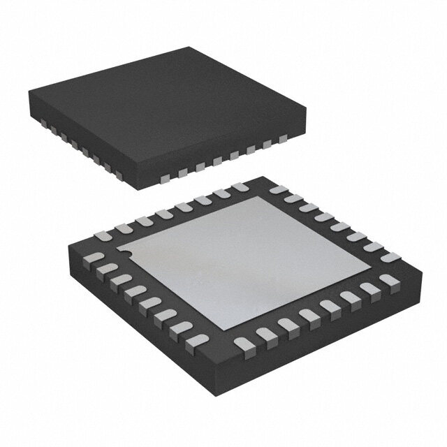
| 产品图片 |
|
| rohs | 符合RoHS无铅 / 符合限制有害物质指令(RoHS)规范要求 |
| 产品系列 | 数据转换器IC,模数转换器 - ADC,Texas Instruments TLV2544ID- |
| 数据手册 | |
| 产品型号 | TLV2544ID |
| 产品培训模块 | http://www.digikey.cn/PTM/IndividualPTM.page?site=cn&lang=zhs&ptm=13240 |
| 产品目录页面 | |
| 产品种类 | 模数转换器 - ADC |
| 位数 | 12 |
| 供应商器件封装 | 16-SOIC N |
| 信噪比 | 70 dB |
| 其它名称 | 296-2981-5 |
| 分辨率 | 12 bit |
| 制造商产品页 | http://www.ti.com/general/docs/suppproductinfo.tsp?distId=10&orderablePartNumber=TLV2544ID |
| 包装 | 管件 |
| 单位重量 | 155.100 mg |
| 商标 | Texas Instruments |
| 安装类型 | 表面贴装 |
| 安装风格 | SMD/SMT |
| 封装 | Tube |
| 封装/外壳 | 16-SOIC(0.154",3.90mm 宽) |
| 封装/箱体 | SOIC-16 |
| 工作温度 | -40°C ~ 85°C |
| 工作电源电压 | 2.7 V to 5.5 V |
| 工厂包装数量 | 40 |
| 接口类型 | 4-Wire, Serial, SPI |
| 数据接口 | DSP,串行,SPI™ |
| 最大功率耗散 | 1110 mW |
| 最大工作温度 | + 85 C |
| 最小工作温度 | - 40 C |
| 标准包装 | 40 |
| 特性 | - |
| 电压参考 | Internal, External |
| 电压源 | 单电源 |
| 系列 | TLV2544 |
| 结构 | SAR |
| 转换器数 | 1 |
| 转换器数量 | 1 |
| 转换速率 | 200 kS/s |
| 输入数和类型 | 4 个单端,单极 |
| 输入类型 | Single-Ended |
| 通道数量 | 4 Channel |
| 采样率(每秒) | 200k |


- 商务部:美国ITC正式对集成电路等产品启动337调查
- 曝三星4nm工艺存在良率问题 高通将骁龙8 Gen1或转产台积电
- 太阳诱电将投资9.5亿元在常州建新厂生产MLCC 预计2023年完工
- 英特尔发布欧洲新工厂建设计划 深化IDM 2.0 战略
- 台积电先进制程称霸业界 有大客户加持明年业绩稳了
- 达到5530亿美元!SIA预计今年全球半导体销售额将创下新高
- 英特尔拟将自动驾驶子公司Mobileye上市 估值或超500亿美元
- 三星加码芯片和SET,合并消费电子和移动部门,撤换高东真等 CEO
- 三星电子宣布重大人事变动 还合并消费电子和移动部门
- 海关总署:前11个月进口集成电路产品价值2.52万亿元 增长14.8%


PDF Datasheet 数据手册内容提取
(cid:1)(cid:2)(cid:3)(cid:4)(cid:5)(cid:6)(cid:6)(cid:7) (cid:1)(cid:2)(cid:3)(cid:4)(cid:5)(cid:6)(cid:8) (cid:4)(cid:9)(cid:10)(cid:11)(cid:3) (cid:1)(cid:12) (cid:5)(cid:9)(cid:5)(cid:11)(cid:3)(cid:7) (cid:13)(cid:4)(cid:11)(cid:14)(cid:15)(cid:1)(cid:7) (cid:4)(cid:16)(cid:16)(cid:11)(cid:17)(cid:18)(cid:19)(cid:18)(cid:7) (cid:6)(cid:11)(cid:20)(cid:8)(cid:11)(cid:21)(cid:22)(cid:23)(cid:24)(cid:24)(cid:25)(cid:2)(cid:7) (cid:2)(cid:12)(cid:26)(cid:11)(cid:19)(cid:12)(cid:26)(cid:25)(cid:27) (cid:18)(cid:25)(cid:27)(cid:15)(cid:23)(cid:2) (cid:23)(cid:24)(cid:23)(cid:2)(cid:12)(cid:28)(cid:11)(cid:1)(cid:12)(cid:11)(cid:29)(cid:15)(cid:28)(cid:15)(cid:1)(cid:23)(cid:2) (cid:21)(cid:12)(cid:24)(cid:3)(cid:25)(cid:27)(cid:1)(cid:25)(cid:27)(cid:18) (cid:26)(cid:15)(cid:1)(cid:22) (cid:23)(cid:30)(cid:1)(cid:12)(cid:19)(cid:12)(cid:26)(cid:25)(cid:27)(cid:11)(cid:29)(cid:12)(cid:26)(cid:24) SLAS198E − FEBRUARY 1999 − REVISED JUNE 2003 (cid:1) (cid:1) Maximum Throughput 200-KSPS Single Wide Range Supply 2.7 Vdc to (cid:1) Built-In Reference, Conversion Clock and 5.5 Vdc 8× FIFO (cid:1) Analog Input Range 0-V to Supply Voltage (cid:1) Differential/Integral Nonlinearity Error: With 500 kHz BW ±1 LSB (cid:1) Hardware Controlled and Programmable (cid:1) Sampling Period Signal-to-Noise and Distortion Ratio: (cid:1) 70 dB, f = 12-kHz Low Operating Current (1.0-mA at 3.3-V, i (cid:1) Spurious Free Dynamic Range: 75 dB, 1.1-mA at 5.5-V With External Ref (cid:1) f = 12- kHz Power Down: Software/Hardware i (cid:1) SPI (CPOL = 0, CPHA = 0)/DSP-Compatible Power-Down Mode (1 µA Max, Ext Ref), Serial Interfaces With SCLK up to 20-MHz Autopower-Down Mode (1 µA, Ext Ref) (cid:1) Programmable Auto-Channel Sweep TLV2548 TLV2544 DW OR PW PACKAGE D OR PW PACKAGE (TOP VIEW) (TOP VIEW) SDO 1 20 CS SDO 1 16 CS SDI 2 19 REFP SDI 2 15 REFP SCLK 3 18 REFM SCLK 3 14 REFM EOC/(INT) 4 17 FS EOC/(INT) 4 13 FS VCC 5 16 PWDN VCC 5 12 PWDN A0 6 15 GND A0 6 11 GND A1 7 14 CSTART A1 7 10 CSTART A2 8 13 A7 A2 8 9 A3 A3 9 12 A6 A4 10 11 A5 description The TLV2548 and TLV2544 are a family of high performance, 12-bit low power, 3.86 µs, CMOS analog-to-digital converters (ADC) which operate from a single 2.7-V to 5.5-V power supply. These devices have three digital inputs and a 3-state output [chip select (CS), serial input-output clock (SCLK), serial data input (SDI), and serial data output (SDO)] that provide a direct 4-wire interface to the serial port of most popular host microprocessors (SPI interface). When interfaced with a TI DSP, a frame sync (FS) signal is used to indicate the start of a serial data frame. In addition to a high-speed A/D converter and versatile control capability, these devices have an on-chip analog multiplexer that can select any analog inputs or one of three internal self-test voltages. The sample-and-hold function is automatically started after the fourth SCLK edge (normal sampling) or can be controlled by a special pin, CSTART, to extend the sampling period (extended sampling). The normal sampling period can also be programmed as short (12 SCLKs) or as long (24 SCLKs) to accommodate faster SCLK operation popular among high-performance signal processors. The TLV2548 and TLV2544 are designed to operate with very low power consumption. The power-saving feature is further enhanced with software/hardware/autopower-down modes and programmable conversion speeds. The conversion clock (OSC) and reference are built-in. The converter can use the external SCLK as the source of the conversion clock to achieve higher (up to 2.8 µs when a 20 MHz SCLK is used) conversion speed. Two different internal reference voltages are available. An optional external reference can also be used to achieve maximum flexibility. The TLV2544C and the TLV2548C are characterized for operation from 0°C to 70°C. The TLV2544I and the TLV2548I are characterized for operation from −40°C to 85°C. Please be aware that an important notice concerning availability, standard warranty, and use in critical applications of TexasInstruments semiconductor products and disclaimers thereto appears at the end of this data sheet. (cid:19)(cid:27)(cid:12)(cid:29)(cid:30)(cid:21)(cid:1)(cid:15)(cid:12)(cid:24) (cid:29)(cid:23)(cid:1)(cid:23) (cid:31)!"#$%&’(cid:31)#! (cid:31)( )*$$+!’ &( #" ,*-.(cid:31))&’(cid:31)#! /&’+(cid:9) Copyright 1999 − 2003, Texas Instruments Incorporated (cid:19)$#/*)’( )#!"#$% ’# (,+)(cid:31)"(cid:31))&’(cid:31)#!( ,+$ ’0+ ’+$%( #" (cid:1)+1&( (cid:15)!(’$*%+!’( (cid:12)! ,$#/*)’( )#%,.(cid:31)&!’ ’# 5(cid:15)(cid:2)(cid:11)(cid:19)(cid:27)6(cid:11)7(cid:8)(cid:5)7(cid:5)(cid:7) &.. ,&$&%+’+$( &$+ ’+(’+/ (’&!/&$/ 2&$$&!’3(cid:9) (cid:19)$#/*)’(cid:31)#! ,$#)+(((cid:31)!4 /#+( !#’ !+)+((&$(cid:31).3 (cid:31)!).*/+ *!.+(( #’0+$2(cid:31)(+ !#’+/(cid:9) (cid:12)! &.. #’0+$ ,$#/*)’((cid:7) ,$#/*)’(cid:31)#! ’+(’(cid:31)!4 #" &.. ,&$&%+’+$((cid:9) ,$#)+(((cid:31)!4 /#+( !#’ !+)+((&$(cid:31).3 (cid:31)!).*/+ ’+(’(cid:31)!4 #" &.. ,&$&%+’+$((cid:9) POST OFFICE BOX 655303 • DALLAS, TEXAS 75265 1
(cid:1)(cid:2)(cid:3)(cid:4)(cid:5)(cid:6)(cid:6)(cid:7) (cid:1)(cid:2)(cid:3)(cid:4)(cid:5)(cid:6)(cid:8) (cid:4)(cid:9)(cid:10)(cid:11)(cid:3) (cid:1)(cid:12) (cid:5)(cid:9)(cid:5)(cid:11)(cid:3)(cid:7) (cid:13)(cid:4)(cid:11)(cid:14)(cid:15)(cid:1)(cid:7) (cid:4)(cid:16)(cid:16)(cid:11)(cid:17)(cid:18)(cid:19)(cid:18)(cid:7) (cid:6)(cid:11)(cid:20)(cid:8)(cid:11)(cid:21)(cid:22)(cid:23)(cid:24)(cid:24)(cid:25)(cid:2)(cid:7) (cid:2)(cid:12)(cid:26)(cid:11)(cid:19)(cid:12)(cid:26)(cid:25)(cid:27) (cid:18)(cid:25)(cid:27)(cid:15)(cid:23)(cid:2) (cid:23)(cid:24)(cid:23)(cid:2)(cid:12)(cid:28)(cid:11)(cid:1)(cid:12)(cid:11)(cid:29)(cid:15)(cid:28)(cid:15)(cid:1)(cid:23)(cid:2) (cid:21)(cid:12)(cid:24)(cid:3)(cid:25)(cid:27)(cid:1)(cid:25)(cid:27)(cid:18) (cid:26)(cid:15)(cid:1)(cid:22) (cid:23)(cid:30)(cid:1)(cid:12)(cid:19)(cid:12)(cid:26)(cid:25)(cid:27)(cid:11)(cid:29)(cid:12)(cid:26)(cid:24) SLAS198E − FEBRUARY 1999 − REVISED JUNE 2003 functional block diagram VCC REFP 4/2 V REFM Reference FIFO 12 Bit × 8 2548 2544 A0 A0 g Low Power A1 X aloUX S/H 12-BIT A2 A1 nM SAR ADC A A3 X OSC A4 A2 INT A5 X A6 A3 Command Conversion A7 X Decode EXT Clock M U SDO CFR X SDI CMR (4 MSBs) DIV SCLK CS FS Control Logic EOC/(INT) CSTART PWDN GND AVAILABLE OPTIONS PACKAGED DEVICES TA 20-TSSOP 20-SOIC 16-SOIC 16-TSSOP 20-CDIP 20-LCCC (PW) (DW) (D) (PW) (J) (FK) 0°C to 70°C TLV2548CPW TLV2548CDW TLV2544CD TLV2544CPW — — −40°C to 85°C TLV2548IPW TLV2548IDW TLV2544ID TLV2544IPW — — 2 POST OFFICE BOX 655303 • DALLAS, TEXAS 75265
(cid:1)(cid:2)(cid:3)(cid:4)(cid:5)(cid:6)(cid:6)(cid:7) (cid:1)(cid:2)(cid:3)(cid:4)(cid:5)(cid:6)(cid:8) (cid:4)(cid:9)(cid:10)(cid:11)(cid:3) (cid:1)(cid:12) (cid:5)(cid:9)(cid:5)(cid:11)(cid:3)(cid:7) (cid:13)(cid:4)(cid:11)(cid:14)(cid:15)(cid:1)(cid:7) (cid:4)(cid:16)(cid:16)(cid:11)(cid:17)(cid:18)(cid:19)(cid:18)(cid:7) (cid:6)(cid:11)(cid:20)(cid:8)(cid:11)(cid:21)(cid:22)(cid:23)(cid:24)(cid:24)(cid:25)(cid:2)(cid:7) (cid:2)(cid:12)(cid:26)(cid:11)(cid:19)(cid:12)(cid:26)(cid:25)(cid:27) (cid:18)(cid:25)(cid:27)(cid:15)(cid:23)(cid:2) (cid:23)(cid:24)(cid:23)(cid:2)(cid:12)(cid:28)(cid:11)(cid:1)(cid:12)(cid:11)(cid:29)(cid:15)(cid:28)(cid:15)(cid:1)(cid:23)(cid:2) (cid:21)(cid:12)(cid:24)(cid:3)(cid:25)(cid:27)(cid:1)(cid:25)(cid:27)(cid:18) (cid:26)(cid:15)(cid:1)(cid:22) (cid:23)(cid:30)(cid:1)(cid:12)(cid:19)(cid:12)(cid:26)(cid:25)(cid:27)(cid:11)(cid:29)(cid:12)(cid:26)(cid:24) SLAS198E − FEBRUARY 1999 − REVISED JUNE 2003 Terminal Functions TERMINAL NO. II//OO DDEESSCCRRIIPPTTIIOONN NNAAMMEE TLV2544 TLV2548 A0 A0 6 6 I Analog signal inputs. The analog inputs are applied to these terminals and are internally A1 A1 7 7 multiplexed. The driving source impedance should be less than or equal to 1 kΩ. A2 A2 8 8 For a source impedance greater than 1 kΩ, use the asynchronous conversion start signal CSTART A3 A3 9 9 (CSTART low time controls the sampling period) or program long sampling period to increase the A4 10 sampling time. A5 11 A6 12 A7 13 CS 16 20 I Chip select. A high-to-low transition on the CS input resets the internal 4-bit counter, enables SDI, and removes SDO from 3-state within a maximum setup time. SDI is disabled within a setup time after the 4-bit counter counts to 16 (clock edges) or a low-to-high transition of CS whichever happens first. NOTE: CS falling and rising edges need to happen when SCLK is low for a microprocessor interface such as SPI. CSTART 10 14 I This terminal controls the start of sampling of the analog input from a selected multiplex channel. Sampling time starts with the falling edge of CSTART and ends with the rising edge of CSTART as long as CS is held high. In mode 01, select cycle, CSTART can be issued as soon as CHANNEL is selected which means the fifth SCLK during the select cycle, but the effective sampling time is not started until CS goes to high. The rising edge of CSTART (when CS = 1) also starts the conversion. Tie this terminal to VCC if not used. EOC/(INT) 4 4 O End of conversion or interrupt to host processor. [PROGRAMMED AS EOC]: This output goes from a high-to-low logic level at the end of the sampling period and remains low until the conversion is complete and data are ready for transfer. EOC is used in conversion mode 00 only. [PROGRAMMED AS INT]: This pin can also be programmed as an interrupt output signal to the host processor. The falling edge of INT indicates data are ready for output. The following CS↓ or FS clears INT. FS 13 17 I DSP frame sync input. Indication of the start of a serial data frame in or out of the device. If FS remains low after the falling edge of CS, SDI is not enabled until an active FS is presented. A high-to-low transition on the FS input resets the internal 4-bit counter and enables SDI within a maximum setup time. SDI is disabled within a setup time after the 4-bit counter counts to 16 (clock edges) or a low-to-high transition of CS whichever happens first. Tie this terminal to VCC if not used. See the date code information section, item (1). GND 11 15 I Ground return for the internal circuitry. Unless otherwise noted, all voltage measurements are with respect to GND. PWDN 12 16 I Both analog and reference circuits are powered down when this pin is at logic zero. The device can be restarted by active CS, FS or CSTART after this pin is pulled back to logic one. SCLK 3 3 I Input serial clock. This terminal receives the serial SCLK from the host processor. SCLK is used to clock the input SDI to the input register. When programmed, it may also be used as the source of the conversion clock. NOTE: This device supports CPOL (clock polarity) = 0, which is SCLK returns to zero when idling for SPI compatible interface. SDI 2 2 I Serial data input. The input data is presented with the MSB (D15) first. The first 4-bit MSBs, D(15−12) are decoded as one of the 16 commands (12 only for the TLV2544). The configure write commands require an additional 12 bits of data. When FS is not used (FS =1), the first MSB (D15) is expected after the falling edge of CS and is latched in on the rising edges of SCLK (after CS↓). When FS is used (typical with an active FS from a DSP) the first MSB (D15) is expected after the falling edge of FS and is latched in on the falling edges of SCLK. SDI is disabled within a setup time after the 4-bit counter counts to 16 (clock edges) or a low-to-high transition of CS whichever happens first. POST OFFICE BOX 655303 • DALLAS, TEXAS 75265 3
(cid:1)(cid:2)(cid:3)(cid:4)(cid:5)(cid:6)(cid:6)(cid:7) (cid:1)(cid:2)(cid:3)(cid:4)(cid:5)(cid:6)(cid:8) (cid:4)(cid:9)(cid:10)(cid:11)(cid:3) (cid:1)(cid:12) (cid:5)(cid:9)(cid:5)(cid:11)(cid:3)(cid:7) (cid:13)(cid:4)(cid:11)(cid:14)(cid:15)(cid:1)(cid:7) (cid:4)(cid:16)(cid:16)(cid:11)(cid:17)(cid:18)(cid:19)(cid:18)(cid:7) (cid:6)(cid:11)(cid:20)(cid:8)(cid:11)(cid:21)(cid:22)(cid:23)(cid:24)(cid:24)(cid:25)(cid:2)(cid:7) (cid:2)(cid:12)(cid:26)(cid:11)(cid:19)(cid:12)(cid:26)(cid:25)(cid:27) (cid:18)(cid:25)(cid:27)(cid:15)(cid:23)(cid:2) (cid:23)(cid:24)(cid:23)(cid:2)(cid:12)(cid:28)(cid:11)(cid:1)(cid:12)(cid:11)(cid:29)(cid:15)(cid:28)(cid:15)(cid:1)(cid:23)(cid:2) (cid:21)(cid:12)(cid:24)(cid:3)(cid:25)(cid:27)(cid:1)(cid:25)(cid:27)(cid:18) (cid:26)(cid:15)(cid:1)(cid:22) (cid:23)(cid:30)(cid:1)(cid:12)(cid:19)(cid:12)(cid:26)(cid:25)(cid:27)(cid:11)(cid:29)(cid:12)(cid:26)(cid:24) SLAS198E − FEBRUARY 1999 − REVISED JUNE 2003 Terminal Functions (Continued) TERMINAL NO. II//OO DDEESSCCRRIIPPTTIIOONN NNAAMMEE TLV2544 TLV2548 SDO 1 1 O The 3-state serial output for the A/D conversion result. SDO is kept in the high-impedance state when CS is high and after the CS falling edge and until the MSB is presented. The output format is MSB first. When FS is not used (FS = 1 at the falling edge of CS), the MSB is presented to the SDO pin after the CS falling edge, and successive data are available at the rising edge of SCLK and changed on the falling edge. When FS is used (FS = 0 at the falling edge of CS), the MSB is presented to SDO after the falling edge of CS and FS = 0 is detected. Successive data are available at the falling edge of SCLK and changed on the rising edge. (This is typically used with an active FS from a DSP.) For conversion and FIFO read cycles, the first 12 bits are result from previous conversion (data) followed by 4 don’t care bits. The first four bits from SDO for CFR read cycles should be ignored. The register content is in the last 12 bits. SDO is 3-state (float) after the 16th bit. See the date code information section, item (2). REFM 14 18 I External reference input or internal reference decoupling. Tie this pin to analog ground if internal reference is used. REFP 15 19 I External reference input or internal reference decoupling. (Shunt capacitors of 10 µF and 0.1 µF between REFP and REFM.) The maximum input voltage range is determined by the difference between the voltage applied to this terminal and the REFM terminal when an external reference is used. VCC 5 5 I Positive supply voltage detailed description analog inputs and internal test voltages The 4/8 analog inputs and three internal test inputs are selected by the analog multiplexer depending on the command entered. The input multiplexer is a break-before-make type to reduce input-to-input noise injection resulting from channel switching. converter The TLV2544/48 uses a 12-bit successive approximation ADC utilizing a charge redistribution DAC. Figure 1 shows a simplified version of the ADC. The sampling capacitor acquires the signal on Ain during the sampling period. When the conversion process starts, the SAR control logic and charge redistribution DAC are used to add and subtract fixed amounts of charge from the sampling capacitor to bring the comparator into a balanced condition. When the comparator is balanced, the conversion is complete and the ADC output code is generated. 4 POST OFFICE BOX 655303 • DALLAS, TEXAS 75265
(cid:1)(cid:2)(cid:3)(cid:4)(cid:5)(cid:6)(cid:6)(cid:7) (cid:1)(cid:2)(cid:3)(cid:4)(cid:5)(cid:6)(cid:8) (cid:4)(cid:9)(cid:10)(cid:11)(cid:3) (cid:1)(cid:12) (cid:5)(cid:9)(cid:5)(cid:11)(cid:3)(cid:7) (cid:13)(cid:4)(cid:11)(cid:14)(cid:15)(cid:1)(cid:7) (cid:4)(cid:16)(cid:16)(cid:11)(cid:17)(cid:18)(cid:19)(cid:18)(cid:7) (cid:6)(cid:11)(cid:20)(cid:8)(cid:11)(cid:21)(cid:22)(cid:23)(cid:24)(cid:24)(cid:25)(cid:2)(cid:7) (cid:2)(cid:12)(cid:26)(cid:11)(cid:19)(cid:12)(cid:26)(cid:25)(cid:27) (cid:18)(cid:25)(cid:27)(cid:15)(cid:23)(cid:2) (cid:23)(cid:24)(cid:23)(cid:2)(cid:12)(cid:28)(cid:11)(cid:1)(cid:12)(cid:11)(cid:29)(cid:15)(cid:28)(cid:15)(cid:1)(cid:23)(cid:2) (cid:21)(cid:12)(cid:24)(cid:3)(cid:25)(cid:27)(cid:1)(cid:25)(cid:27)(cid:18) (cid:26)(cid:15)(cid:1)(cid:22) (cid:23)(cid:30)(cid:1)(cid:12)(cid:19)(cid:12)(cid:26)(cid:25)(cid:27)(cid:11)(cid:29)(cid:12)(cid:26)(cid:24) SLAS198E − FEBRUARY 1999 − REVISED JUNE 2003 detailed description (continued) Charge Redistribution DAC _ Ain Control ADC Code + Logic REFM Figure 1. Simplified Model of the Successive-Approximation System serial interface INPUT DATA FORMAT MSB LSB D15−D12 D11−D0 Command ID[15:12] Configuration data field ID[11:0] Input data is binary. All trailing blanks can be filled with zeros. OUTPUT DATA FORMAT READ CFR/FIFO READ MSB LSB D15−D12 D11−D0 Don’t care Register content or FIFO content OD[11:0] OUTPUT DATA FORMAT CONVERSION MSB LSB D15−D4 D3−D0 Conversion result OD[11:0] Don’t care The output data format is binary (unipolar straight binary). binary Zero scale code = 000h, Vcode = VREFM Full scale code = FFFh, Vcode = VREFP − 1 LSB POST OFFICE BOX 655303 • DALLAS, TEXAS 75265 5
(cid:1)(cid:2)(cid:3)(cid:4)(cid:5)(cid:6)(cid:6)(cid:7) (cid:1)(cid:2)(cid:3)(cid:4)(cid:5)(cid:6)(cid:8) (cid:4)(cid:9)(cid:10)(cid:11)(cid:3) (cid:1)(cid:12) (cid:5)(cid:9)(cid:5)(cid:11)(cid:3)(cid:7) (cid:13)(cid:4)(cid:11)(cid:14)(cid:15)(cid:1)(cid:7) (cid:4)(cid:16)(cid:16)(cid:11)(cid:17)(cid:18)(cid:19)(cid:18)(cid:7) (cid:6)(cid:11)(cid:20)(cid:8)(cid:11)(cid:21)(cid:22)(cid:23)(cid:24)(cid:24)(cid:25)(cid:2)(cid:7) (cid:2)(cid:12)(cid:26)(cid:11)(cid:19)(cid:12)(cid:26)(cid:25)(cid:27) (cid:18)(cid:25)(cid:27)(cid:15)(cid:23)(cid:2) (cid:23)(cid:24)(cid:23)(cid:2)(cid:12)(cid:28)(cid:11)(cid:1)(cid:12)(cid:11)(cid:29)(cid:15)(cid:28)(cid:15)(cid:1)(cid:23)(cid:2) (cid:21)(cid:12)(cid:24)(cid:3)(cid:25)(cid:27)(cid:1)(cid:25)(cid:27)(cid:18) (cid:26)(cid:15)(cid:1)(cid:22) (cid:23)(cid:30)(cid:1)(cid:12)(cid:19)(cid:12)(cid:26)(cid:25)(cid:27)(cid:11)(cid:29)(cid:12)(cid:26)(cid:24) SLAS198E − FEBRUARY 1999 − REVISED JUNE 2003 control and timing power up and initialization requirements (cid:1) Determine processor type by writing A000h to the TLV2544/48 (CS must be toggled) (cid:1) Configure the device (CS must make a high-to-low transition, then can be held low if in DSP mode; i.e., active FS.) The first conversion after power up or resuming from power down is not valid. start of the cycle: (cid:1) When FS is not used (FS = 1 at the falling edge of CS), the falling edge of CS is the start of the cycle. (cid:1) When FS is used (FS is an active signal from a DSP), the falling edge of FS is the start of the cycle. first 4-MSBs: the command register (CMR) The TLV2544/TLV2548 have a 4-bit command set (see Table 1) plus a 12-bit configuration data field. Most of the commands require only the first 4 MSBs, i.e., without the 12-bit data field. The valid commands are listed in Table 1. Table 1. TLV2544/TLV2548 Command Set SDI D(15−12) BINARY TLV2548 COMMAND TLV2544 COMMAND 0000b 0h Select analog input channel 0 Select analog input channel 0 0001b 1h Select analog input channel 1 N/A 0010b 2h Select analog input channel 2 Select analog input channel 1 0011b 3h Select analog input channel 3 N/A 0100b 4h Select analog input channel 4 Select analog input channel 2 0101b 5h Select analog input channel 5 N/A 0110b 6h Select analog input channel 6 Select analog input channel 3 0111b 7h Select analog input channel 7 N/A 1000b 8h SW power down (analog + reference) 1001b 9h Read CFR register data shown as SDO D(11−0) Write CFR followed by 12-bit data, e.g., 0A100h means external reference, 1010b Ah plus data short sampling, SCLK/4, single shot, INT 1011b Bh Select test, voltage = (REFP+REFM)/2 1100b Ch Select test, voltage = REFM 1101b Dh Select test, voltage = REFP 1110b Eh FIFO read, FIFO contents shown as SDO D(15−4), D(3−0) = 0000 11111111bb FFhh pplluuss ddaattaa RReesseerrvveedd NOTE: The status of the CFR can be read with a read CFR command when the device is programmed for one-shot conversion mode (CFR D[6,5] = 00). 6 POST OFFICE BOX 655303 • DALLAS, TEXAS 75265
(cid:1)(cid:2)(cid:3)(cid:4)(cid:5)(cid:6)(cid:6)(cid:7) (cid:1)(cid:2)(cid:3)(cid:4)(cid:5)(cid:6)(cid:8) (cid:4)(cid:9)(cid:10)(cid:11)(cid:3) (cid:1)(cid:12) (cid:5)(cid:9)(cid:5)(cid:11)(cid:3)(cid:7) (cid:13)(cid:4)(cid:11)(cid:14)(cid:15)(cid:1)(cid:7) (cid:4)(cid:16)(cid:16)(cid:11)(cid:17)(cid:18)(cid:19)(cid:18)(cid:7) (cid:6)(cid:11)(cid:20)(cid:8)(cid:11)(cid:21)(cid:22)(cid:23)(cid:24)(cid:24)(cid:25)(cid:2)(cid:7) (cid:2)(cid:12)(cid:26)(cid:11)(cid:19)(cid:12)(cid:26)(cid:25)(cid:27) (cid:18)(cid:25)(cid:27)(cid:15)(cid:23)(cid:2) (cid:23)(cid:24)(cid:23)(cid:2)(cid:12)(cid:28)(cid:11)(cid:1)(cid:12)(cid:11)(cid:29)(cid:15)(cid:28)(cid:15)(cid:1)(cid:23)(cid:2) (cid:21)(cid:12)(cid:24)(cid:3)(cid:25)(cid:27)(cid:1)(cid:25)(cid:27)(cid:18) (cid:26)(cid:15)(cid:1)(cid:22) (cid:23)(cid:30)(cid:1)(cid:12)(cid:19)(cid:12)(cid:26)(cid:25)(cid:27)(cid:11)(cid:29)(cid:12)(cid:26)(cid:24) SLAS198E − FEBRUARY 1999 − REVISED JUNE 2003 control and timing (continued) configuration Configuration data is stored in one 12-bit configuration register (CFR) (see Table 2 for CFR bit definitions). Once configured after first power up, the information is retained in the H/W or S/W power down state. When the device is being configured, a write CFR cycle is issued by the host processor. This is a 16-bit write. If the SCLK stops after the first 8 bits are entered, then the next eight bits can be taken after the SCLK is resumed. Table 2. TLV2544/TLV2548 Configuration Register (CFR) Bit Definitions BIT DEFINITION D11 Reference select 0: External 1: Internal (Tie REFM to analog ground if the Internal reference is selected.) D10 Internal reference voltage select 0: Internal ref = 4 V 1: internal ref = 2 V D9 Sample period select 0: Short sampling 12 SCLKs (1x sampling time) 1: Long sampling 24 SCLKs (2x sampling time) D(8,7) Conversion clock source select 00: Conversion clock = internal OSC 01: Conversion clock = SCLK 10: Conversion clock = SCLK/4 11: Conversion clock = SCLK/2 D(6,5) Conversion mode select 00: Single shot mode [FIFO not used, D(1,0) has no effect.] 01: Repeat mode 10: Sweep mode 11: Repeat sweep mode DD((44,,33))† TLV2548 TLV2544 Sweep auto sequence select Sweep auto sequence select 00: 0−1−2−3−4−5−6−7 00: N/A 01: 0−2−4−6−0−2−4−6 01: 0−1−2−3−0−1−2−3 10: 0−0−2−2−4−4−6−6 10: 0−0−1−1−2−2−3−3 11: 0−2−0−2−0−2−0−2 11: 0−1−0−1−0−1−0−1 D2 EOC/INT − pin function select 0: Pin used as INT 1: Pin used as EOC D(1,0) FIFO trigger level (sweep sequence length) 00: Full (INT generated after FIFO level 7 filled) 01: 3/4 (INT generated after FIFO level 5 filled) 10: 1/2 (INT generated after FIFO level 3 filled) 11: 1/4 (INT generated after FIFO level 1 filled) †These bits only take effect in conversion modes 10 and 11. sampling The sampling period starts after the first 4 input data are shifted in if they are decoded as one of the conversion commands. These are select analog input (channel 0 through 7) and select test (channel 1 through 3). POST OFFICE BOX 655303 • DALLAS, TEXAS 75265 7
(cid:1)(cid:2)(cid:3)(cid:4)(cid:5)(cid:6)(cid:6)(cid:7) (cid:1)(cid:2)(cid:3)(cid:4)(cid:5)(cid:6)(cid:8) (cid:4)(cid:9)(cid:10)(cid:11)(cid:3) (cid:1)(cid:12) (cid:5)(cid:9)(cid:5)(cid:11)(cid:3)(cid:7) (cid:13)(cid:4)(cid:11)(cid:14)(cid:15)(cid:1)(cid:7) (cid:4)(cid:16)(cid:16)(cid:11)(cid:17)(cid:18)(cid:19)(cid:18)(cid:7) (cid:6)(cid:11)(cid:20)(cid:8)(cid:11)(cid:21)(cid:22)(cid:23)(cid:24)(cid:24)(cid:25)(cid:2)(cid:7) (cid:2)(cid:12)(cid:26)(cid:11)(cid:19)(cid:12)(cid:26)(cid:25)(cid:27) (cid:18)(cid:25)(cid:27)(cid:15)(cid:23)(cid:2) (cid:23)(cid:24)(cid:23)(cid:2)(cid:12)(cid:28)(cid:11)(cid:1)(cid:12)(cid:11)(cid:29)(cid:15)(cid:28)(cid:15)(cid:1)(cid:23)(cid:2) (cid:21)(cid:12)(cid:24)(cid:3)(cid:25)(cid:27)(cid:1)(cid:25)(cid:27)(cid:18) (cid:26)(cid:15)(cid:1)(cid:22) (cid:23)(cid:30)(cid:1)(cid:12)(cid:19)(cid:12)(cid:26)(cid:25)(cid:27)(cid:11)(cid:29)(cid:12)(cid:26)(cid:24) SLAS198E − FEBRUARY 1999 − REVISED JUNE 2003 normal sampling When the converter is using normal sampling, the sampling period is programmable. It can be 12 SCLKs (short sampling) or 24 SCLKs (long sampling). Long sampling helps when SCLK is faster than 10 MHz or when input source resistance is high. extended sampling CSTART − An asynchronous (to the SCLK) signal, via dedicated hardware pin, CSTART, can be used in order to have total control of the sampling period and the start of a conversion. This extended sampling is user-defined and is totally independent of SCLK. While CS is high, the falling edge of CSTART is the start of the sampling period and is controlled by the low time of CSTART. The minimum low time for CSTART should be at least equal to the minimum t . In a select cycle used in mode 01 (REPEAT MODE), CSTART can be started as soon (SAMPLE) as the channel is selected (after the fifth SCLK). In this case the sampling period is not started until CS has become inactive. Therefore the nonoverlapped CSTART low time must meet the minimum sampling time requirement. The low-to-high transition of CSTART terminates the sampling period and starts the conversion period. The conversion clock can also be configured to use either internal OSC or external SCLK. This function is useful for an application that requires: (cid:1) The use of an extended sampling period to accommodate different input source impedance (cid:1) The use of a faster I/O clock on the serial port but not enough sampling time is available due to the fixed number of SCLKs. This could be due to a high input source impedance or due to higher MUX ON resistance at lower supply voltage. Once the conversion is complete, the processor can initiate a read cycle by using either the read FIFO command to read the conversion result or by simply selecting the next channel number for conversion. Since the device has a valid conversion result in the output buffer, the conversion result is simply presented at the serial data output. To completely get out of the extended sampling mode, CS must be toggled twice from a high-to-low transition while CSTART is high. The read cycle mentioned above followed by another configuration cycle of the ADC qualifies this condition and successfully puts the ADC back to its normal sampling mode. This can be viewed in Figure 9. Table 3. Sample and Convert Conditions CONDITIONS SAMPLE CONVERT No sampling clock (SCLK) required. Sampling period is totally controlled by the low time of CSTART. The high-to-low transition of CSTART (when CS=1) CS = 1 starts the sampling of the analog input signal. The low CSTART (see Figures time of CSTART dictates the sampling period. The 11 and 18) low-to-high transition of CSTART ends sampling period and begins the conversion cycle. (Note: this trigger only works when internal reference is selected for conversion modes 01, 10, and 11.) 11)) IIff tthhee iinntteerrnnaall cclloocckk OOSSCC iiss sseelleecctteedd aa mmaaxxiimmuumm SCLK is required. Sampling period is programmable conversion time of 3.86 µs can be achieved. under normal sampling. When programmed to sample 2) If external SCLK is selected, conversion time is CS CSTART = 1 under short sampling, 12 SCLKs are generated to tconv= 14 × DIV/f(SCLK), where DIV can be 1, 2, or FS = 1 complete sampling period. 24 SCLKs are generated 4. when programmed for long sampling. A command set to configure the device requires 4 SCLKs thereby ex- tteennddiinngg ttoo 1166 oorr 2288 SSCCLLKKss rreessppeeccttiivveellyy bbeeffoorree ccoonnvveerr-- sion takes place. (Note: Because the ADC only bypasses a valid channel select command, the user CSTART = 1 can use select channel 0, 0000b, as the SDI input FS CS = 0 when either CS or FS is used as trigger for conversion. The ADC responds to commands such as SW power- down, 1000b.) 8 POST OFFICE BOX 655303 • DALLAS, TEXAS 75265
(cid:1)(cid:2)(cid:3)(cid:4)(cid:5)(cid:6)(cid:6)(cid:7) (cid:1)(cid:2)(cid:3)(cid:4)(cid:5)(cid:6)(cid:8) (cid:4)(cid:9)(cid:10)(cid:11)(cid:3) (cid:1)(cid:12) (cid:5)(cid:9)(cid:5)(cid:11)(cid:3)(cid:7) (cid:13)(cid:4)(cid:11)(cid:14)(cid:15)(cid:1)(cid:7) (cid:4)(cid:16)(cid:16)(cid:11)(cid:17)(cid:18)(cid:19)(cid:18)(cid:7) (cid:6)(cid:11)(cid:20)(cid:8)(cid:11)(cid:21)(cid:22)(cid:23)(cid:24)(cid:24)(cid:25)(cid:2)(cid:7) (cid:2)(cid:12)(cid:26)(cid:11)(cid:19)(cid:12)(cid:26)(cid:25)(cid:27) (cid:18)(cid:25)(cid:27)(cid:15)(cid:23)(cid:2) (cid:23)(cid:24)(cid:23)(cid:2)(cid:12)(cid:28)(cid:11)(cid:1)(cid:12)(cid:11)(cid:29)(cid:15)(cid:28)(cid:15)(cid:1)(cid:23)(cid:2) (cid:21)(cid:12)(cid:24)(cid:3)(cid:25)(cid:27)(cid:1)(cid:25)(cid:27)(cid:18) (cid:26)(cid:15)(cid:1)(cid:22) (cid:23)(cid:30)(cid:1)(cid:12)(cid:19)(cid:12)(cid:26)(cid:25)(cid:27)(cid:11)(cid:29)(cid:12)(cid:26)(cid:24) SLAS198E − FEBRUARY 1999 − REVISED JUNE 2003 TLV2544/TLV2548 conversion modes The TLV2544 and TLV2548 have four different conversion modes (mode 00, 01, 10, 11). The operation of each mode is slightly different, depending on how the converter performs the sampling and which host interface is used. The trigger for a conversion can be an active CSTART (extended sampling), CS (normal sampling, SPI interface), or FS (normal sampling, TMS320 DSP interface). When FS is used as the trigger, CS can be held active, i.e. CS does not need to be toggled through the trigger sequence. SDI can be one of the channel select commands, such as SELECT CHANNEL 0. Different types of triggers should not be mixed throughout the repeat and sweep operations. When CSTART is used as the trigger, the conversion starts on the rising edge of CSTART. The minimum low time for CSTART is equal to t . If an active CS or FS is used as the trigger, (SAMPLE) the conversion is started after the 16th or 28th SCLK edge. Enough time (for conversion) should be allowed between consecutive triggers so that no conversion is terminated prematurely. one shot mode (mode 00) One shot mode (mode 00) does not use the FIFO, and the EOC is generated as the conversion is in progress (or INT is generated after the conversion is done). repeat mode (mode 01) Repeat mode (mode 01) uses the FIFO. This mode setup requires configuration cycle and channel select cycle. Once the programmed FIFO threshold is reached, the FIFO must be read, or the data is lost when the sequence starts over again with the SELECT cycle and series of triggers. No configuration is required except for reselecting the channel unless the operation mode is changed. This allows the host to set up the converter and continue monitoring a fixed input and come back to get a set of samples when preferred. Triggered by CSTART: The first conversion can be started with a select cycle or CSTART. To do so, the user can issue CSTART during the select cycle, immediately after the four-bit channel select command. The first sample started as soon as the select cycle is finished (i.e., CS returns to 1). If there is enough time (2 µs) left between the SELECT cycle and the following CSTART, a conversion is carried out. In this case, you need one less trigger to fill the FIFO. Succeeding samples are triggered by CSTART. sweep mode (mode 10) Sweep mode (mode 10) also uses the FIFO. Once it is programmed in this mode, all of the channels listed in the selected sweep sequence are visited in sequence. The results are converted and stored in the FIFO. This sweep sequence may not be completed if the FIFO threshold is reached before the list is completed. This allows the system designer to change the sweep sequence length. Once the FIFO has reached its programmed threshold, an interrupt (INT) is generated. The host must issue a read FIFO command to read and clear the FIFO before the next sweep can start. repeat sweep mode (mode 11) Repeat sweep mode (mode 11) works the same way as mode 10 except the operation has an option to continue even if the FIFO threshold is reached. Once the FIFO has reached its programmed threshold, an interrupt (INT) is generated. Then two things may happen: 1. The host may choose to act on it (read the FIFO) or ignore it. If the next cycle is a read FIFO cycle, all of the data stored in the FIFO is retained until it has been read in order. 2. If the next cycle is not a read FIFO cycle, or another CSTART is generated, all of the content stored in the FIFO is cleared before the next conversion result is stored in the FIFO, and the sweep is continued. POST OFFICE BOX 655303 • DALLAS, TEXAS 75265 9
(cid:1)(cid:2)(cid:3)(cid:4)(cid:5)(cid:6)(cid:6)(cid:7) (cid:1)(cid:2)(cid:3)(cid:4)(cid:5)(cid:6)(cid:8) (cid:4)(cid:9)(cid:10)(cid:11)(cid:3) (cid:1)(cid:12) (cid:5)(cid:9)(cid:5)(cid:11)(cid:3)(cid:7) (cid:13)(cid:4)(cid:11)(cid:14)(cid:15)(cid:1)(cid:7) (cid:4)(cid:16)(cid:16)(cid:11)(cid:17)(cid:18)(cid:19)(cid:18)(cid:7) (cid:6)(cid:11)(cid:20)(cid:8)(cid:11)(cid:21)(cid:22)(cid:23)(cid:24)(cid:24)(cid:25)(cid:2)(cid:7) (cid:2)(cid:12)(cid:26)(cid:11)(cid:19)(cid:12)(cid:26)(cid:25)(cid:27) (cid:18)(cid:25)(cid:27)(cid:15)(cid:23)(cid:2) (cid:23)(cid:24)(cid:23)(cid:2)(cid:12)(cid:28)(cid:11)(cid:1)(cid:12)(cid:11)(cid:29)(cid:15)(cid:28)(cid:15)(cid:1)(cid:23)(cid:2) (cid:21)(cid:12)(cid:24)(cid:3)(cid:25)(cid:27)(cid:1)(cid:25)(cid:27)(cid:18) (cid:26)(cid:15)(cid:1)(cid:22) (cid:23)(cid:30)(cid:1)(cid:12)(cid:19)(cid:12)(cid:26)(cid:25)(cid:27)(cid:11)(cid:29)(cid:12)(cid:26)(cid:24) SLAS198E − FEBRUARY 1999 − REVISED JUNE 2003 TLV2544/TLV2548 conversion modes (continued) Table 4. TLV2544/TLV2548 Conversion Mode CONVERSION CFR SAMPLING OPERATION MODE D(6,5) TYPE One shot 00 Normal • Single conversion from a selected channel • CS or FS to start select/sampling/conversion/read • One INT or EOC generated after each conversion • Host must serve INT by selecting channel, and converting and reading the previous output. Extended • Single conversion from a selected channel • CS to select/read • CSTART to start sampling and conversion • One INT or EOC generated after each conversion • Host must serve INT by selecting next channel and reading the previous output. Repeat 01 Normal • Repeated conversions from a selected channel • CS or FS to start sampling/conversion • One INT generated after FIFO is filled up to the threshold • Host must serve INT by either 1) (FIFO read) reading out all of the FIFO contents up to the threshold, then repeat conversions from the same selected channel or 2) writing another command(s) to change the conversion mode. If the FIFO is not read when INT is served, it is cleared. Extended • Same as normal sampling except CSTART starts each sampling and conversion when CS is high. Sweep 10 Normal • One conversion per channel from a sequence of channels • CS or FS to start sampling/conversion • One INT generated after FIFO is filled up to the threshold • Host must serve INT by (FIFO read) reading out all of the FIFO contents up to the threshold, then write another command(s) to change the conversion mode. Extended • Same as normal sampling except CSTART starts each sampling and conversion when CS is high. Repeat sweep 11 Normal • Repeated conversions from a sequence of channels • CS or FS to start sampling/conversion • One INT generated after FIFO is filled up to the threshold • Host must serve INT by either 1) (FIFO read) reading out all of the FIFO contents up to the threshold, then repeat conversions from the same selected channel or 2) writing another command(s) to change the conversion mode. If the FIFO is not read when INT is served it is cleared. Extended • Same as normal sampling except CSTART starts each sampling and conversion when CS is high. NOTES: 1. Programming the EOC/INT pin as the EOC signal works for mode 00 only. The other three modes automatically generate an INT signal irrespective of how EOC/INT is programmed. 2. Extended. Sampling mode using CSTART as the trigger only works when internal reference is selected for conversion modes 01, 10, and 11. 3. When using CSTART to sample in extended mode, the falling edge of the next CSTART trigger should occur no more than 2.5 µs after the falling CS edge (or falling FS edge if FS is active) of the channel select cycle. This is to prevent an ongoing conversion from being canceled. 10 POST OFFICE BOX 655303 • DALLAS, TEXAS 75265
(cid:1)(cid:2)(cid:3)(cid:4)(cid:5)(cid:6)(cid:6)(cid:7) (cid:1)(cid:2)(cid:3)(cid:4)(cid:5)(cid:6)(cid:8) (cid:4)(cid:9)(cid:10)(cid:11)(cid:3) (cid:1)(cid:12) (cid:5)(cid:9)(cid:5)(cid:11)(cid:3)(cid:7) (cid:13)(cid:4)(cid:11)(cid:14)(cid:15)(cid:1)(cid:7) (cid:4)(cid:16)(cid:16)(cid:11)(cid:17)(cid:18)(cid:19)(cid:18)(cid:7) (cid:6)(cid:11)(cid:20)(cid:8)(cid:11)(cid:21)(cid:22)(cid:23)(cid:24)(cid:24)(cid:25)(cid:2)(cid:7) (cid:2)(cid:12)(cid:26)(cid:11)(cid:19)(cid:12)(cid:26)(cid:25)(cid:27) (cid:18)(cid:25)(cid:27)(cid:15)(cid:23)(cid:2) (cid:23)(cid:24)(cid:23)(cid:2)(cid:12)(cid:28)(cid:11)(cid:1)(cid:12)(cid:11)(cid:29)(cid:15)(cid:28)(cid:15)(cid:1)(cid:23)(cid:2) (cid:21)(cid:12)(cid:24)(cid:3)(cid:25)(cid:27)(cid:1)(cid:25)(cid:27)(cid:18) (cid:26)(cid:15)(cid:1)(cid:22) (cid:23)(cid:30)(cid:1)(cid:12)(cid:19)(cid:12)(cid:26)(cid:25)(cid:27)(cid:11)(cid:29)(cid:12)(cid:26)(cid:24) SLAS198E − FEBRUARY 1999 − REVISED JUNE 2003 timing diagrams The timing diagrams can be categorized into two major groups: nonconversion and conversion. The nonconversion cycles are read and write (configuration). None of these cycles carry a conversion. Conversion cycles are those four modes of conversion. read cycle (read FIFO or read CFR) read CFR cycle: The read command is decoded in the first 4 clocks. SDO outputs the contents of the CFR after the 4th SCLK. This command works only when the device is programmed in the single shot mode (mode 00). 1 2 3 4 5 6 7 12 13 14 15 16 1 SCLK CS FS ÏÏÏÏÏÏÏÏÏÏÏÏÏÏÏÏÏÏÏÏ SDI ID15 ID14 ID13 ID12 ID15 ÏÏÏÏÏÏÏÏÏÏÏÏÏÏÏÏÏÏÏÏ INT EOC ÏÏÏÏÏÏÏ ÏÏÏÏ SDO ÏÏÏÏÏÏÏOD11 OD10 OD9 OD4 OD3 OD2 OD1 OD0 ÏÏÏÏ Figure 2. TLV2544/TLV2548 Read CFR Cycle (FS active) 1 2 3 4 5 6 7 12 13 14 15 16 1 SCLK CS FS ÏÏÏ ÏÏÏÏÏÏÏÏÏÏÏÏÏÏÏÏÏÏÏÏ SDI ID15 ID14 ID13 ID12 ID15 ID14 INT EOC ÏÏÏÏÏÏ ÏÏÏ SDO ÏÏÏÏÏÏOD11 OD10 OD9 OD4 OD3 OD2 OD1 OD0 ÏÏÏ Figure 3. TLV2544/TLV2548 Read CFR Cycle (FS = 1) POST OFFICE BOX 655303 • DALLAS, TEXAS 75265 11
(cid:1)(cid:2)(cid:3)(cid:4)(cid:5)(cid:6)(cid:6)(cid:7) (cid:1)(cid:2)(cid:3)(cid:4)(cid:5)(cid:6)(cid:8) (cid:4)(cid:9)(cid:10)(cid:11)(cid:3) (cid:1)(cid:12) (cid:5)(cid:9)(cid:5)(cid:11)(cid:3)(cid:7) (cid:13)(cid:4)(cid:11)(cid:14)(cid:15)(cid:1)(cid:7) (cid:4)(cid:16)(cid:16)(cid:11)(cid:17)(cid:18)(cid:19)(cid:18)(cid:7) (cid:6)(cid:11)(cid:20)(cid:8)(cid:11)(cid:21)(cid:22)(cid:23)(cid:24)(cid:24)(cid:25)(cid:2)(cid:7) (cid:2)(cid:12)(cid:26)(cid:11)(cid:19)(cid:12)(cid:26)(cid:25)(cid:27) (cid:18)(cid:25)(cid:27)(cid:15)(cid:23)(cid:2) (cid:23)(cid:24)(cid:23)(cid:2)(cid:12)(cid:28)(cid:11)(cid:1)(cid:12)(cid:11)(cid:29)(cid:15)(cid:28)(cid:15)(cid:1)(cid:23)(cid:2) (cid:21)(cid:12)(cid:24)(cid:3)(cid:25)(cid:27)(cid:1)(cid:25)(cid:27)(cid:18) (cid:26)(cid:15)(cid:1)(cid:22) (cid:23)(cid:30)(cid:1)(cid:12)(cid:19)(cid:12)(cid:26)(cid:25)(cid:27)(cid:11)(cid:29)(cid:12)(cid:26)(cid:24) SLAS198E − FEBRUARY 1999 − REVISED JUNE 2003 read cycle (read FIFO or read CFR) (continued) FIFO read cycle The first command in the active cycle after INT is generated, if the FIFO is used, is assumed as the FIFO read command. The first FIFO content is output immediately before the command is decoded. If this command is not a FIFO read, then the output is terminated but the first data in the FIFO is retained until a valid FIFO read command is decoded. Use of more layers of the FIFO reduces the time taken to read multiple data. This is because the read cycle does not generate EOC or INT, nor does it carry out any conversion. 1 2 3 4 5 6 7 12 13 14 15 16 1 2 SCLK CS FS ÏÏÏ ÏÏÏÏÏÏÏÏÏÏÏÏÏÏÏÏÏÏÏÏ SDI ID15 ID14 ID13 ID12 ID15 ID14 ÏÏÏ ÏÏÏÏÏÏÏÏÏÏÏÏÏÏÏÏÏÏÏÏ INT EOC ÏÏÏÏÏÏÏ SDO OD11OD10 OD9 OD8 OD7 OD6 OD5 OD0 OD11OD10 ÏÏÏÏÏÏÏ These devices can perform continuous FIFO read cycles (FS = 1) controlled by SCLK; SCLK can stop between each 16 SCLKs. Figure 4. TLV2544/TLV2548 FIFO Read Cycle (FS = 1) 12 POST OFFICE BOX 655303 • DALLAS, TEXAS 75265
(cid:1)(cid:2)(cid:3)(cid:4)(cid:5)(cid:6)(cid:6)(cid:7) (cid:1)(cid:2)(cid:3)(cid:4)(cid:5)(cid:6)(cid:8) (cid:4)(cid:9)(cid:10)(cid:11)(cid:3) (cid:1)(cid:12) (cid:5)(cid:9)(cid:5)(cid:11)(cid:3)(cid:7) (cid:13)(cid:4)(cid:11)(cid:14)(cid:15)(cid:1)(cid:7) (cid:4)(cid:16)(cid:16)(cid:11)(cid:17)(cid:18)(cid:19)(cid:18)(cid:7) (cid:6)(cid:11)(cid:20)(cid:8)(cid:11)(cid:21)(cid:22)(cid:23)(cid:24)(cid:24)(cid:25)(cid:2)(cid:7) (cid:2)(cid:12)(cid:26)(cid:11)(cid:19)(cid:12)(cid:26)(cid:25)(cid:27) (cid:18)(cid:25)(cid:27)(cid:15)(cid:23)(cid:2) (cid:23)(cid:24)(cid:23)(cid:2)(cid:12)(cid:28)(cid:11)(cid:1)(cid:12)(cid:11)(cid:29)(cid:15)(cid:28)(cid:15)(cid:1)(cid:23)(cid:2) (cid:21)(cid:12)(cid:24)(cid:3)(cid:25)(cid:27)(cid:1)(cid:25)(cid:27)(cid:18) (cid:26)(cid:15)(cid:1)(cid:22) (cid:23)(cid:30)(cid:1)(cid:12)(cid:19)(cid:12)(cid:26)(cid:25)(cid:27)(cid:11)(cid:29)(cid:12)(cid:26)(cid:24) SLAS198E − FEBRUARY 1999 − REVISED JUNE 2003 write cycle (write CFR) The write cycle is used to write to the configuration register CFR (with 12-bit register content). The write cycle does not generate an EOC or INT, nor does it carry out any conversion (see power up and initialization requirements). 1 2 3 4 5 6 7 12 13 14 15 16 1 SCLK CS FS ÏÏÏÏ ÏÏÏÏÏÏÏÏÏ SDÏI ÏÏÏID15 ID14 ID13 ID12 ID11 ID10 ID9 ID4 ID3 ID2 ID1 IÏD0 ÏÏÏÏÏÏÏÏID15 INT EOC ÏÏÏÏÏÏÏÏÏÏÏÏÏÏÏÏÏÏÏÏÏ ÏÏÏÏÏ SDO ÏÏÏÏÏÏÏÏÏÏÏÏÏÏÏÏÏÏÏÏÏ ÏÏÏÏÏ Figure 5. TLV2544/TLV2548 Write Cycle (FS Active) 1 2 3 4 5 6 7 12 13 14 15 16 1 SCLK CS FS ÏÏÏ ÏÏÏÏÏÏÏÏ SDI ID15 ID14 ID13 ID12 ID11 ID10 ID9 ID4 ID3 ID2 ID1 ID0 ID15 ID14 INT EOC ÏÏÏÏÏÏÏÏÏÏÏÏÏÏÏÏÏÏÏ ÏÏÏÏ ÏÏÏÏÏÏÏÏÏÏÏÏÏÏÏÏÏÏÏ ÏÏÏÏ SDO Figure 6. TLV2544/TLV2548 Write Cycle (FS = 1) POST OFFICE BOX 655303 • DALLAS, TEXAS 75265 13
(cid:1)(cid:2)(cid:3)(cid:4)(cid:5)(cid:6)(cid:6)(cid:7) (cid:1)(cid:2)(cid:3)(cid:4)(cid:5)(cid:6)(cid:8) (cid:4)(cid:9)(cid:10)(cid:11)(cid:3) (cid:1)(cid:12) (cid:5)(cid:9)(cid:5)(cid:11)(cid:3)(cid:7) (cid:13)(cid:4)(cid:11)(cid:14)(cid:15)(cid:1)(cid:7) (cid:4)(cid:16)(cid:16)(cid:11)(cid:17)(cid:18)(cid:19)(cid:18)(cid:7) (cid:6)(cid:11)(cid:20)(cid:8)(cid:11)(cid:21)(cid:22)(cid:23)(cid:24)(cid:24)(cid:25)(cid:2)(cid:7) (cid:2)(cid:12)(cid:26)(cid:11)(cid:19)(cid:12)(cid:26)(cid:25)(cid:27) (cid:18)(cid:25)(cid:27)(cid:15)(cid:23)(cid:2) (cid:23)(cid:24)(cid:23)(cid:2)(cid:12)(cid:28)(cid:11)(cid:1)(cid:12)(cid:11)(cid:29)(cid:15)(cid:28)(cid:15)(cid:1)(cid:23)(cid:2) (cid:21)(cid:12)(cid:24)(cid:3)(cid:25)(cid:27)(cid:1)(cid:25)(cid:27)(cid:18) (cid:26)(cid:15)(cid:1)(cid:22) (cid:23)(cid:30)(cid:1)(cid:12)(cid:19)(cid:12)(cid:26)(cid:25)(cid:27)(cid:11)(cid:29)(cid:12)(cid:26)(cid:24) SLAS198E − FEBRUARY 1999 − REVISED JUNE 2003 conversion cycles DSP/normal sampling 16 − Short Sampling 30 − Short Sampling (If CONV 28 − Long Sampling 42 − Long Sampling CLK = SCLK0 1 2 3 4 5 6 7 12 SCLK tc (30 or 42 SCLKs) CS FS ÏÏÏ ÏÏÏÏÏÏÏÏÏÏÏÏÏÏÏÏÏÏÏÏÏÏ SDIÏÏÏID15 ID14 ID13 ID12ÏÏÏÏÏÏÏÏÏÏÏÏÏÏÏÏÏÏÏÏÏÏID15 INT t(sample) (12 or 24 SCLKs) EOC (SDOZ on SCLK16L Regardless ÏÏÏÏÏÏ of Sampling Time) t(conv) SDO MSB MSB-1 MSB-2 MSB-3 MSB-4 MSB-5 MSB-6 LSBÏÏÏÏÏÏ MSB Figure 7. Mode 00 Single Shot/Normal Sampling (FS Signal Used) 16 − Short Sampling 30 − Short Sampling (If CONV 28 − Long Sampling 42 − Long Sampling CLK = SCLK0 1 2 3 4 5 6 7 12 13 1 SCLK tc (30 or 42 SCLKs) CS FS ÏÏÏÏ ÏÏÏÏÏÏÏÏÏÏÏÏÏÏÏÏÏÏÏÏÏ ÏÏÏÏ ÏÏÏÏÏÏÏÏÏÏÏÏÏÏÏÏÏÏÏÏÏ SDI ID15 ID14 ID13 ID12 ID15 INT t(sample) (12 or 24 SCLKs) EOC (SDOZ on SCLK16L Regardless of Sampling Time) ÏÏÏÏÏÏÏt(conv) SDO MSB MSB-1 MSB-2 MSB-3 MSB-4 MSB-5 MSB-6 LSB MSB ÏÏÏÏÏÏÏ Figure 8. Mode 00 Single Shot/Normal Sampling (FS = 1, FS Signal not Used) 14 POST OFFICE BOX 655303 • DALLAS, TEXAS 75265
(cid:1)(cid:2)(cid:3)(cid:4)(cid:5)(cid:6)(cid:6)(cid:7) (cid:1)(cid:2)(cid:3)(cid:4)(cid:5)(cid:6)(cid:8) (cid:4)(cid:9)(cid:10)(cid:11)(cid:3) (cid:1)(cid:12) (cid:5)(cid:9)(cid:5)(cid:11)(cid:3)(cid:7) (cid:13)(cid:4)(cid:11)(cid:14)(cid:15)(cid:1)(cid:7) (cid:4)(cid:16)(cid:16)(cid:11)(cid:17)(cid:18)(cid:19)(cid:18)(cid:7) (cid:6)(cid:11)(cid:20)(cid:8)(cid:11)(cid:21)(cid:22)(cid:23)(cid:24)(cid:24)(cid:25)(cid:2)(cid:7) (cid:2)(cid:12)(cid:26)(cid:11)(cid:19)(cid:12)(cid:26)(cid:25)(cid:27) (cid:18)(cid:25)(cid:27)(cid:15)(cid:23)(cid:2) (cid:23)(cid:24)(cid:23)(cid:2)(cid:12)(cid:28)(cid:11)(cid:1)(cid:12)(cid:11)(cid:29)(cid:15)(cid:28)(cid:15)(cid:1)(cid:23)(cid:2) (cid:21)(cid:12)(cid:24)(cid:3)(cid:25)(cid:27)(cid:1)(cid:25)(cid:27)(cid:18) (cid:26)(cid:15)(cid:1)(cid:22) (cid:23)(cid:30)(cid:1)(cid:12)(cid:19)(cid:12)(cid:26)(cid:25)(cid:27)(cid:11)(cid:29)(cid:12)(cid:26)(cid:24) SLAS198E − FEBRUARY 1999 − REVISED JUNE 2003 conversion cycles (continued) Device Get Out Device Going Into Extended Sampling Select/Read Extended Sampling Mode Select/Read Read Mode Cycle Cycle Cycle CS t(sample ) Normal CSTART Cycle FS ÏÏÏÏÏÏÏÏÏt(coÏnv) ÏÏÏÏÏÏÏÏÏÏÏÏÏÏÏÏÏÏÏÏÏÏ SDÏI ÏÏφ ÏÏÏÏÏÏÏÏÏÏÏφ ÏÏÏÏÏÏÏÏÏÏÏÏÏÏÏÏ INT EOC Previous Conversion Previous Conversion Result Result Hi-Z Hi-Z Hi-Z ÏÏÏÏ SDO †This is one of the single shot commands. Conversion starts on next rising edge of CSTART. Figure 9. Mode 00 Single Shot/Extended Sampling (FS Signal Used, FS Pin Connected to TMS320 DSP) modes using the FIFO: modes 01, 10, 11 timing Conversion #1 Conversion #4 Configure Select From Channel 2 From Channel 2 Select CS FS CSTART ÏÏÏÏÏÏÏÏÏÏÏÏÏÏÏÏÏÏÏÏÏÏÏÏÏÏÏÏÏÏÏÏ † § ¶ ¶ ¶ ‡ ‡ ‡ ‡ § ¶ SDI ÏÏÏÏÏÏÏÏÏÏÏÏÏÏÏÏÏÏÏÏÏÏÏÏÏÏÏÏÏÏÏÏ INT ÏÏÏÏÏ ÏÏ Hi-Z Hi-Z SDO ÏÏÏÏÏ ÏÏ Read FIFO #1 #2 #3 #4 Top of FIFO †Command = Configure write for mode 01, FIFO threshold = 1/2 ‡Command = Read FIFO, first FIFO read §Command = Select ch2. ¶Use any channel select command to trigger SDI input. Figure 10. TLV2544/TLV2548 Mode 01 DSP Serial Interface (Conversions Triggered by FS) POST OFFICE BOX 655303 • DALLAS, TEXAS 75265 15
(cid:1)(cid:2)(cid:3)(cid:4)(cid:5)(cid:6)(cid:6)(cid:7) (cid:1)(cid:2)(cid:3)(cid:4)(cid:5)(cid:6)(cid:8) (cid:4)(cid:9)(cid:10)(cid:11)(cid:3) (cid:1)(cid:12) (cid:5)(cid:9)(cid:5)(cid:11)(cid:3)(cid:7) (cid:13)(cid:4)(cid:11)(cid:14)(cid:15)(cid:1)(cid:7) (cid:4)(cid:16)(cid:16)(cid:11)(cid:17)(cid:18)(cid:19)(cid:18)(cid:7) (cid:6)(cid:11)(cid:20)(cid:8)(cid:11)(cid:21)(cid:22)(cid:23)(cid:24)(cid:24)(cid:25)(cid:2)(cid:7) (cid:2)(cid:12)(cid:26)(cid:11)(cid:19)(cid:12)(cid:26)(cid:25)(cid:27) (cid:18)(cid:25)(cid:27)(cid:15)(cid:23)(cid:2) (cid:23)(cid:24)(cid:23)(cid:2)(cid:12)(cid:28)(cid:11)(cid:1)(cid:12)(cid:11)(cid:29)(cid:15)(cid:28)(cid:15)(cid:1)(cid:23)(cid:2) (cid:21)(cid:12)(cid:24)(cid:3)(cid:25)(cid:27)(cid:1)(cid:25)(cid:27)(cid:18) (cid:26)(cid:15)(cid:1)(cid:22) (cid:23)(cid:30)(cid:1)(cid:12)(cid:19)(cid:12)(cid:26)(cid:25)(cid:27)(cid:11)(cid:29)(cid:12)(cid:26)(cid:24) SLAS198E − FEBRUARY 1999 − REVISED JUNE 2003 modes using the FIFO: modes 01, 10, 11 timing (continued) Conversion #1 From Channel 2 Conversion #4 From Channel 2 Configure Select Select CS ¶ FS (DSP) t(sample) t(sample) t(sample) t(sample) CSTART ÏÏÏÏÏÏÏÏÏÏÏÏÏÏÏÏÏÏÏÏÏÏÏÏÏÏÏÏÏÏÏÏÏ SDIÏφÏϧÏÏÏÏÏÏÏÏÏÏÏχ ÏÏχ Ïχ χÏÏϧ ÏÏÏÏÏÏÏÏ INT ÏÏÏÏ ÏÏÏ Hi-Z Hi-Z ÏÏÏÏ ÏÏÏ SDO Sample Times ≥ MIN t(sample) Read FIFO #1 #2 #3 #4 First FIFO Read (See Operating Characteristics) †Command = Configure write for mode 01, FIFO threshold = 1/2 ‡Command = Read FIFO, first FIFO read §Command = Select ch2. ¶Minimum CS low time for select cycle is 6 SCLKs. The same amount of time is required between FS low to CSTART for proper channel decoding. The low time of CSTART, not overlapped with CS low time, is the valid sampling time for the select cycle (see Figure 18). Figure 11. TLV2544/TLV2548 Mode 01 µp/DSP Serial Interface (Conversions Triggered by CSTART) Conversion Conversion Conversion Conversion From Channel 3 From Channel 0 From Channel 3 Configure From Channel 0 CS FS (DSP) CSTART ÏÏÏÏÏÏÏÏÏÏÏÏÏÏÏÏÏÏÏÏÏÏÏÏÏÏÏÏÏÏÏÏÏ SDI † § § § § ‡ ‡ ‡ ‡ § § § § ‡ ÏÏÏÏÏÏÏÏÏÏÏÏÏÏÏÏÏÏÏÏÏÏÏÏÏÏÏÏÏÏÏÏÏ INT ÏÏ SDO ÏÏ Repeat Read FIFO #1 #2 #3 #4 Repeat Read FIFO #1 Top of FIFO First FIFO Read Second FIFO Read †Command = Configure write for mode 10 or 11, FIFO threshold = 1/2, sweep seq = 0−1−2−3. ‡Command = Read FIFO §Use any channel select command to trigger SDI input. Figure 12. TLV2544/TLV2548 Mode 10/11 DSP Serial Interface (Conversions Triggered by FS) 16 POST OFFICE BOX 655303 • DALLAS, TEXAS 75265
(cid:1)(cid:2)(cid:3)(cid:4)(cid:5)(cid:6)(cid:6)(cid:7) (cid:1)(cid:2)(cid:3)(cid:4)(cid:5)(cid:6)(cid:8) (cid:4)(cid:9)(cid:10)(cid:11)(cid:3) (cid:1)(cid:12) (cid:5)(cid:9)(cid:5)(cid:11)(cid:3)(cid:7) (cid:13)(cid:4)(cid:11)(cid:14)(cid:15)(cid:1)(cid:7) (cid:4)(cid:16)(cid:16)(cid:11)(cid:17)(cid:18)(cid:19)(cid:18)(cid:7) (cid:6)(cid:11)(cid:20)(cid:8)(cid:11)(cid:21)(cid:22)(cid:23)(cid:24)(cid:24)(cid:25)(cid:2)(cid:7) (cid:2)(cid:12)(cid:26)(cid:11)(cid:19)(cid:12)(cid:26)(cid:25)(cid:27) (cid:18)(cid:25)(cid:27)(cid:15)(cid:23)(cid:2) (cid:23)(cid:24)(cid:23)(cid:2)(cid:12)(cid:28)(cid:11)(cid:1)(cid:12)(cid:11)(cid:29)(cid:15)(cid:28)(cid:15)(cid:1)(cid:23)(cid:2) (cid:21)(cid:12)(cid:24)(cid:3)(cid:25)(cid:27)(cid:1)(cid:25)(cid:27)(cid:18) (cid:26)(cid:15)(cid:1)(cid:22) (cid:23)(cid:30)(cid:1)(cid:12)(cid:19)(cid:12)(cid:26)(cid:25)(cid:27)(cid:11)(cid:29)(cid:12)(cid:26)(cid:24) SLAS198E − FEBRUARY 1999 − REVISED JUNE 2003 modes using the FIFO: modes 01, 10, 11 timing (continued) Conversion Conversion Conversion Conversion From Channel 0 From Channel 3 From Channel 3 From Channel 0 Configure CS FS (DSP) CSTART t(sample) t(sample) t(sample) t(sample) ÏÏÏÏÏÏÏÏÏÏÏÏÏÏÏÏÏÏÏÏÏÏÏÏÏÏÏÏÏÏÏÏÏ SDI † ‡ ‡ ‡ ‡ ‡ ÏÏÏÏÏÏÏÏÏÏÏÏÏÏÏÏÏÏÏÏÏÏÏÏÏÏÏÏÏÏÏÏÏ INT SDO Read FIFO #1 #2 #3 #4 Read FIFO #1 Repeat Repeat Top of FIFO Second FIFO Read First FIFO Read †Command = Configure write for mode 10 or 11, FIFO threshold = 1/2, sweep seq = 0−1−2−3. ‡Command = Read FIFO Figure 13. TLV2544/TLV2548 Mode 10/11 DSP Serial Interface (Conversions Triggered by CSTART) Conversion Conversion Conversion Conversion From Channel 0 From Channel 3 From Channel 0 From Channel 3 Configure CS CSTART SDÏI Ïφ ÏϧÏÏϧ ÏϧÏϧÏÏχ χÏχÏχÏϧÏϧÏϧ Ïϧ ÏÏ‡Ï INT SDO Read FIFO #1 #2 #3 #4 Read FIFO #1 Repeat Top of FIFO Repeat First FIFO Read Second FIFO Read †Command = Configure write for mode 10 or 11, FIFO threshold = 1/2, sweep seq = 0−1−2−3. ‡Command = Read FIFO §Use any channel select command to trigger SDI input. Figure 14. TLV2544/TLV2548 Mode 10/11 µp Serial Interface (Conversions Triggered by CS) POST OFFICE BOX 655303 • DALLAS, TEXAS 75265 17
(cid:1)(cid:2)(cid:3)(cid:4)(cid:5)(cid:6)(cid:6)(cid:7) (cid:1)(cid:2)(cid:3)(cid:4)(cid:5)(cid:6)(cid:8) (cid:4)(cid:9)(cid:10)(cid:11)(cid:3) (cid:1)(cid:12) (cid:5)(cid:9)(cid:5)(cid:11)(cid:3)(cid:7) (cid:13)(cid:4)(cid:11)(cid:14)(cid:15)(cid:1)(cid:7) (cid:4)(cid:16)(cid:16)(cid:11)(cid:17)(cid:18)(cid:19)(cid:18)(cid:7) (cid:6)(cid:11)(cid:20)(cid:8)(cid:11)(cid:21)(cid:22)(cid:23)(cid:24)(cid:24)(cid:25)(cid:2)(cid:7) (cid:2)(cid:12)(cid:26)(cid:11)(cid:19)(cid:12)(cid:26)(cid:25)(cid:27) (cid:18)(cid:25)(cid:27)(cid:15)(cid:23)(cid:2) (cid:23)(cid:24)(cid:23)(cid:2)(cid:12)(cid:28)(cid:11)(cid:1)(cid:12)(cid:11)(cid:29)(cid:15)(cid:28)(cid:15)(cid:1)(cid:23)(cid:2) (cid:21)(cid:12)(cid:24)(cid:3)(cid:25)(cid:27)(cid:1)(cid:25)(cid:27)(cid:18) (cid:26)(cid:15)(cid:1)(cid:22) (cid:23)(cid:30)(cid:1)(cid:12)(cid:19)(cid:12)(cid:26)(cid:25)(cid:27)(cid:11)(cid:29)(cid:12)(cid:26)(cid:24) SLAS198E − FEBRUARY 1999 − REVISED JUNE 2003 FIFO operation Serial SDO 12-BIT×8 FIFO ADC 7 6 5 4 3 2 1 0 FIFO Full FIFO 1/2 Full FIFO 3/4 Full FIFO 1/4 Full FIFO Threshold Pointer Figure 15. TLV2544/TLV2548 FIFO The device has an 8-layer FIFO that can be programmed for different thresholds. An interrupt is sent to the host after the preprogrammed threshold is reached. The FIFO can be used to store data from either a fixed channel or a series of channels based on a preprogrammed sweep sequence. For example, an application may require eight measurements from channel 3. In this case, the FIFO is filled with eight data sequentially taken from channel 3. Another application may require data from channel 0, channel 2, channel 4, and channel 6 in an orderly manner. Therefore, the threshold is set for 1/2 and the sweep sequence 0−2−4−6−0−2−4−6 is chosen. An interrupt is sent to the host as soon as all four data are in the FIFO. In single shot mode, the FIFO automatically uses a 1/8 FIFO depth. Therefore the CFR bits (D1,0) controlling FIFO depth are don’t care. SCLK and conversion speed There are two ways to adjust the conversion speed. (cid:1) The SCLK can be used as the source of the conversion clock to get the highest throughput of the device. The minimum onboard OSC is 3.6 MHz and 14 conversion clocks are required to complete a conversion. (Corresponding 3.86µs conversion time) The devices can operate with an SCLK up to 20MHz for the supply voltage range specified. When a more accurate conversion time is desired, the SCLK can be used as the source of the conversion clock. The clock divider provides speed options appropriate for an application where a high speed SCLK is used for faster I/O. The total conversion time is 14 ×(DIV/f ) where DIV is 1, SCLK 2, or 4. For example a 20 MHz SCLK with the divide by 4 option produces a {14 × (4/20 M)} = 2.8 µs conversion time. When an external serial clock (SCLK) is used as the source of the conversion clock, the maximum equivalent conversion clock (f /DIV) should not exceed 6 MHz. SCLK (cid:1) Autopower down can be used to slow down the device at a reduced power consumption level. This mode is always used by the converter. If the device is not accessed (by CS or CSTART), the converter is powered down to save power. The built-in reference is left on in order to quickly resume operation within one half SCLK period. This provides unlimited choices to trade speed with power savings. reference voltage The device has a built-in reference with a programmable level of 2 V or 4 V. If the internal reference is used, REFP is set to 2 V or 4 V and REFM should be connected to the analog ground of the converter. An external reference can also be used through two reference input pins, REFP and REFM, if the reference source is programmed as external. The voltage levels applied to these pins establish the upper and lower limits of the analog inputs to produce a full-scale and zero-scale reading respectively. The values of REFP, REFM, and the analog input should not exceed the positive supply or be lower than GND consistent with the specified absolute maximum ratings. The digital output is at full scale when the input signal is equal to or higher than REFP and at zero when the input signal is equal to or lower than REFM. 18 POST OFFICE BOX 655303 • DALLAS, TEXAS 75265
(cid:1)(cid:2)(cid:3)(cid:4)(cid:5)(cid:6)(cid:6)(cid:7) (cid:1)(cid:2)(cid:3)(cid:4)(cid:5)(cid:6)(cid:8) (cid:4)(cid:9)(cid:10)(cid:11)(cid:3) (cid:1)(cid:12) (cid:5)(cid:9)(cid:5)(cid:11)(cid:3)(cid:7) (cid:13)(cid:4)(cid:11)(cid:14)(cid:15)(cid:1)(cid:7) (cid:4)(cid:16)(cid:16)(cid:11)(cid:17)(cid:18)(cid:19)(cid:18)(cid:7) (cid:6)(cid:11)(cid:20)(cid:8)(cid:11)(cid:21)(cid:22)(cid:23)(cid:24)(cid:24)(cid:25)(cid:2)(cid:7) (cid:2)(cid:12)(cid:26)(cid:11)(cid:19)(cid:12)(cid:26)(cid:25)(cid:27) (cid:18)(cid:25)(cid:27)(cid:15)(cid:23)(cid:2) (cid:23)(cid:24)(cid:23)(cid:2)(cid:12)(cid:28)(cid:11)(cid:1)(cid:12)(cid:11)(cid:29)(cid:15)(cid:28)(cid:15)(cid:1)(cid:23)(cid:2) (cid:21)(cid:12)(cid:24)(cid:3)(cid:25)(cid:27)(cid:1)(cid:25)(cid:27)(cid:18) (cid:26)(cid:15)(cid:1)(cid:22) (cid:23)(cid:30)(cid:1)(cid:12)(cid:19)(cid:12)(cid:26)(cid:25)(cid:27)(cid:11)(cid:29)(cid:12)(cid:26)(cid:24) SLAS198E − FEBRUARY 1999 − REVISED JUNE 2003 reference block equivalent circuit INTERNAL REF Close = Int Ref Used Open = Ext Ref Used REFP Sample Convert 10 µF 0.1 µF Internal ~50 pF Decoupling Reference CDAC Cap Compensation Cap REFM (See Note A) External to the Device NOTES: A. If internal reference is used, tie REFM to analog ground and install a 10 µF (or 4.7 µF) internal reference compensation capacitor between REFP and REFM to store the charge as shown in the figure above. B. If external reference is used, the 10 µF (internal reference compensation) capacitor is optional. REFM can be connected to external REFM or AGND. C. Internal reference voltage drift, due to temperature variations, is approximately ±10 mV about the nominal 2 V (typically) from −10°C to 100°C. The nominal value also varies approximately ±50 mV across devices. D. Internal reference leakage during low ON time: Leakage resistance is on the order of 100 MΩ or more. This means the time constant is about 1000 s with 10 µF compensation capacitance. Since the REF voltage does not vary much, the reference comes up quickly after resuming from auto power down. At power up and power down the internal reference sees a glitch of about 500 µV when 2V internal reference is used (1 mV when 4 V internal reference is used). This glitch settles out after about 50 µs. power down The device has three power-down modes. autopower-down mode The device enters the autopower-down state at the end of a conversion. In autopower-down, the power consumption reduces to about 1 mA when an internal reference is selected. The built-in reference is still on to allow the device to resume quickly. The resumption is fast enough (within 0.5 SCLK) for use between cycles. An active CS, FS, or CSTART resumes the device from power-down state. The power current is 1 µA when an external reference is programmed and SCLK stops. hardware/software power-down mode Writing 8000h to the device puts the device into a software power down state, and the entire chip (including the built-in reference) is powered down. For a hardware power-down, the dedicated PWDN pin provides another way to power down the device asynchronously. These two power-down modes power down the entire device including the built-in reference to save power. The power down current is reduced to about 1 µA is the SCLK is stopped. An active CS, FS, or CSTART restores the device. There is no time delay when an external reference is selected. However, if an internal reference is used, it takes about 20 ms to warm up. Deselect PWDN pin to remove the device from the hardware power-down state. This requires about 20 ms to warm up if an internal reference is also selected. The configuration register is not affected by any of the power down modes but the sweep operation sequence has to be started over again. All FIFO contents are cleared by the power-down modes. POST OFFICE BOX 655303 • DALLAS, TEXAS 75265 19
(cid:1)(cid:2)(cid:3)(cid:4)(cid:5)(cid:6)(cid:6)(cid:7) (cid:1)(cid:2)(cid:3)(cid:4)(cid:5)(cid:6)(cid:8) (cid:4)(cid:9)(cid:10)(cid:11)(cid:3) (cid:1)(cid:12) (cid:5)(cid:9)(cid:5)(cid:11)(cid:3)(cid:7) (cid:13)(cid:4)(cid:11)(cid:14)(cid:15)(cid:1)(cid:7) (cid:4)(cid:16)(cid:16)(cid:11)(cid:17)(cid:18)(cid:19)(cid:18)(cid:7) (cid:6)(cid:11)(cid:20)(cid:8)(cid:11)(cid:21)(cid:22)(cid:23)(cid:24)(cid:24)(cid:25)(cid:2)(cid:7) (cid:2)(cid:12)(cid:26)(cid:11)(cid:19)(cid:12)(cid:26)(cid:25)(cid:27) (cid:18)(cid:25)(cid:27)(cid:15)(cid:23)(cid:2) (cid:23)(cid:24)(cid:23)(cid:2)(cid:12)(cid:28)(cid:11)(cid:1)(cid:12)(cid:11)(cid:29)(cid:15)(cid:28)(cid:15)(cid:1)(cid:23)(cid:2) (cid:21)(cid:12)(cid:24)(cid:3)(cid:25)(cid:27)(cid:1)(cid:25)(cid:27)(cid:18) (cid:26)(cid:15)(cid:1)(cid:22) (cid:23)(cid:30)(cid:1)(cid:12)(cid:19)(cid:12)(cid:26)(cid:25)(cid:27)(cid:11)(cid:29)(cid:12)(cid:26)(cid:24) SLAS198E − FEBRUARY 1999 − REVISED JUNE 2003 absolute maximum ratings over operating free-air temperature (unless otherwise noted)† Supply voltage range, GND to V . . . . . . . . . . . . . . . . . . . . . . . . . . . . . . . . . . . . . . . . . . . . . . . . . −0.3 V to 6.5 V CC Analog input voltage range . . . . . . . . . . . . . . . . . . . . . . . . . . . . . . . . . . . . . . . . . . . . . . . . . . . −0.3 V to VCC + 0.3 V Reference input voltage . . . . . . . . . . . . . . . . . . . . . . . . . . . . . . . . . . . . . . . . . . . . . . . . . . . . . . . . . . . . . VCC + 0.3 V Digital input voltage range . . . . . . . . . . . . . . . . . . . . . . . . . . . . . . . . . . . . . . . . . . . . . . . . . . . −0.3 V to VCC + 0.3 V Operating virtual junction temperature range, TJ . . . . . . . . . . . . . . . . . . . . . . . . . . . . . . . . . . . . . −55°C to 150°C Operating free-air temperature range, T : TLV2544/48C . . . . . . . . . . . . . . . . . . . . . . . . . . . . . . . . 0°C to 70°C A TLV2544/48I . . . . . . . . . . . . . . . . . . . . . . . . . . . . . . . −40°C to 85°C Storage temperature range, Tstg . . . . . . . . . . . . . . . . . . . . . . . . . . . . . . . . . . . . . . . . . . . . . . . . . . . −65°C to 150°C Lead temperature 1,6 mm (1/16 inch) from case for 10 seconds . . . . . . . . . . . . . . . . . . . . . . . . . . . . . . . 260°C †Stresses beyond those listed under “absolute maximum ratings” may cause permanent damage to the device. These are stress ratings only, and functional operation of the device at these or any other conditions beyond those indicated under “recommended operating conditions” is not implied. Exposure to absolute-maximum-rated conditions for extended periods may affect device reliability. DISSIPATION RATING TABLE TTAA ≤≤ 2255°CC DDEERRAATTIINNGG FFAACCTTOORR TTAA == 7700°CC TTAA == 8855°CC TTAA == 112255°CC PPAACCKKAAGGEE POWER RATING ABOVE TA = 25°C‡‡ POWER RATING POWER RATING POWER RATING D 1110 mW 8.9 mW/°C 710 mW 577 mW 222 mW DW 1294 mW 10.4 mW/°C 828 mW 673 mW 259 mW 16 PW 839 mW 6.7 mW/°C 537 mW 437 mW — 20 PW 977 mW 7.8 mW/°C 625 mW 508 mW — ‡This is the inverse of the traditional junction-to-ambient thermal resistance (RΘJA). Thermal resistance is not production tested and the values given are for informational purposes only. recommended operating conditions MIN NOM MAX UNIT Supply voltage, VCC 2.7 3.3 5.5 V Analog input voltage (see Note 4) 0 VCC V High level control input voltage, VIH 2.1 V Low-level control input voltage, VIL 0.6 V Delay time, delay from CS falling edge to FS rising edge, td(CSL-FSH) 0.5 SCLKs (See Figure 16) Delay time, delay time from 16th SCLK falling edge to CS rising edge (FS = 1), or 0.5 SCLKs 17th rising edge (FS is active) td(SCLK-CSH) (See Figures 16, and 19) Setup time, FS rising edge before SCLK falling edge, tsu(FSH-SCLKL 20 ns (See Figure 16) Hold time, FS hold high after SCLK falling edge, th(FSH-SCLKL) (See Figure 16) 30 ns Pulse width, CS high time, twH(CS) (See Figures 16 and 19) 100 ns Pulse width, FS high time, twH(FS) (See Figure 16) 0.75 1 SCLKs SSCCLLKK ccyyccllee ttiimmee,, ttcc((SSCCLLKK)) VCC = 2.7 V to 3.6 V 75 10000 nnss (See Figures 16, and 19) VCC = 4.5 V to 5.5V 50 10000 NOTE 4: When binary output format is used, analog input voltages greater than that applied to REFP convert as all ones (111111111111), while input voltages less than that applied to REFM convert as all zeros (000000000000). The device is functional with reference down to 1 V. (VREFP − VREFM − 1); however, the electrical specifications are no longer applicable. 20 POST OFFICE BOX 655303 • DALLAS, TEXAS 75265
(cid:1)(cid:2)(cid:3)(cid:4)(cid:5)(cid:6)(cid:6)(cid:7) (cid:1)(cid:2)(cid:3)(cid:4)(cid:5)(cid:6)(cid:8) (cid:4)(cid:9)(cid:10)(cid:11)(cid:3) (cid:1)(cid:12) (cid:5)(cid:9)(cid:5)(cid:11)(cid:3)(cid:7) (cid:13)(cid:4)(cid:11)(cid:14)(cid:15)(cid:1)(cid:7) (cid:4)(cid:16)(cid:16)(cid:11)(cid:17)(cid:18)(cid:19)(cid:18)(cid:7) (cid:6)(cid:11)(cid:20)(cid:8)(cid:11)(cid:21)(cid:22)(cid:23)(cid:24)(cid:24)(cid:25)(cid:2)(cid:7) (cid:2)(cid:12)(cid:26)(cid:11)(cid:19)(cid:12)(cid:26)(cid:25)(cid:27) (cid:18)(cid:25)(cid:27)(cid:15)(cid:23)(cid:2) (cid:23)(cid:24)(cid:23)(cid:2)(cid:12)(cid:28)(cid:11)(cid:1)(cid:12)(cid:11)(cid:29)(cid:15)(cid:28)(cid:15)(cid:1)(cid:23)(cid:2) (cid:21)(cid:12)(cid:24)(cid:3)(cid:25)(cid:27)(cid:1)(cid:25)(cid:27)(cid:18) (cid:26)(cid:15)(cid:1)(cid:22) (cid:23)(cid:30)(cid:1)(cid:12)(cid:19)(cid:12)(cid:26)(cid:25)(cid:27)(cid:11)(cid:29)(cid:12)(cid:26)(cid:24) SLAS198E − FEBRUARY 1999 − REVISED JUNE 2003 recommended operating conditions (continued) MIN NOM MAX UNIT Pulse width, SCLK low time, twL(SCLK) (See Figures 16 and 19) 0.4 0.6 SCLKs Pulse width, SCLK high time, twH(SCLK) (See Figures 16 and 19) 0.4 0.6 SCLKs Setup time, SDI valid before falling edge of SCLK (FS is active) or the rising edge of 25 ns SCLK (FS=1), tsu(DI-SCLK (See Figures 16 and 19) Hold time, SDI hold valid after falling edge of SCLK (FS is active) or the rising edge 5 ns of SCLK (FS=1), th(DI-SCLK) (See Figure 16) Delay time, delay from CS falling edge to SDO valid, td(CSL-DOV) 25 ns (See Figures 16 and 19) Delay time, delay from FS falling edge to SDO valid, td(FSL-DOV) (See Figure 16) 25 ns 0.5 SCLK SDO = 5 pF 0.5 SCLK + 9 DDeellaayy ttiimmee,, ddeellaayy ffrroomm SSCCLLKK ffaalllliinngg eeddggee ((FFSS iiss VVCCCC == 44..55 VV 0.5 SCLK active) or SCLK rising edge (FS=1) to SDO valid, SDO = 25 pF 0.5 SCLK + 10 ttdd((SSCCLLKK--DDOOVV)).. ((SSeeee FFiigguurreess 1166 aanndd 1199)).. nnss 0.5 SCLK For a date code later than xxx, see the date code SDO = 5 pF 0.5 SCLK iinnffoorrmmaattiioonn iitteemm ((33)).. + 18 VVCCCC == 22..77 VV 0.5 SCLK SDO = 25 pF 0.5 SCLK + 19 Delay time, delay from 17th SCLK rising edge (FS is active) or the 16th falling edge 45 ns (FS=1) to EOC falling edge, td(SCLK-EOCL) (See Figures 16 and 19) Delay time, delay from 16th SCLK falling edge to INT falling edge (FS =1) or from the 17th rising edge SCLK to INT falling edge (when FS active), td(SCLK-INTL) Min t(conv) µs (See Figure 19) Delay time, delay from CS falling edge or FS rising edge to INT rising edge, 1 50 ns td(CSL-INTH) or td(FSH-INTH). See Figures 16, 17, 18 and 19) Delay time, delay from CS rising edge to CSTART falling edge, td(CSH-CSTARTL) 100 ns (See Figures 17 and 18) Delay time, delay from CSTART rising edge to EOC falling edge, td(CSTARTH-EOCL) 1 50 ns (See Figures 17 and 18) Pulse width, CSTART low time, twL(CSTART) (See Figures 17 and 18) Min t(sample) µs Delay time, delay from CSTART rising edge to CSTART falling edge, td(CSTARTH-CSTARTL) (See Figure 18) Max t(conv) µs D(Seelaey F tiigmuere, sd e1l7a ya nfrdo m18 C)START rising edge to INT falling edge, td(CSTARTH-INTL) Max t(conv) µs TLV2544C/TLV2548C 0 70 OOppeerraattiinngg ffrreeee--aaiirr tteemmppeerraattuurree,, TTAA °°CC TLV2544I/TLV2548I −40 85 POST OFFICE BOX 655303 • DALLAS, TEXAS 75265 21
(cid:1)(cid:2)(cid:3)(cid:4)(cid:5)(cid:6)(cid:6)(cid:7) (cid:1)(cid:2)(cid:3)(cid:4)(cid:5)(cid:6)(cid:8) (cid:4)(cid:9)(cid:10)(cid:11)(cid:3) (cid:1)(cid:12) (cid:5)(cid:9)(cid:5)(cid:11)(cid:3)(cid:7) (cid:13)(cid:4)(cid:11)(cid:14)(cid:15)(cid:1)(cid:7) (cid:4)(cid:16)(cid:16)(cid:11)(cid:17)(cid:18)(cid:19)(cid:18)(cid:7) (cid:6)(cid:11)(cid:20)(cid:8)(cid:11)(cid:21)(cid:22)(cid:23)(cid:24)(cid:24)(cid:25)(cid:2)(cid:7) (cid:2)(cid:12)(cid:26)(cid:11)(cid:19)(cid:12)(cid:26)(cid:25)(cid:27) (cid:18)(cid:25)(cid:27)(cid:15)(cid:23)(cid:2) (cid:23)(cid:24)(cid:23)(cid:2)(cid:12)(cid:28)(cid:11)(cid:1)(cid:12)(cid:11)(cid:29)(cid:15)(cid:28)(cid:15)(cid:1)(cid:23)(cid:2) (cid:21)(cid:12)(cid:24)(cid:3)(cid:25)(cid:27)(cid:1)(cid:25)(cid:27)(cid:18) (cid:26)(cid:15)(cid:1)(cid:22) (cid:23)(cid:30)(cid:1)(cid:12)(cid:19)(cid:12)(cid:26)(cid:25)(cid:27)(cid:11)(cid:29)(cid:12)(cid:26)(cid:24) SLAS198E − FEBRUARY 1999 − REVISED JUNE 2003 electrical characteristics over recommended operating free-air temperature range, V = V = 2.7 V to CC REFP 5.5 V, V = 0 V, SCLK frequency = 20 MHz at 5 V, 15 MHz at 3 V (unless otherwise noted) REFM PARAMETER TEST CONDITIONS MIN TYP† MAX UNIT VCC = 5.5 V, IOH = −0.2 mA at 25 pF load 2.4 VVOOHH HHiigghh--lleevveell oouuttppuutt vvoollttaaggee VCC = 2.7 V, IOH = -20 µA at 25 pF load VCC−0.2 VV VCC = 5.5 V, IOL = 0.8 mA at 25 pF load 0.4 VVOOLL LLooww--lleevveell oouuttppuutt vvoollttaaggee VCC = 2.7 V, IOL = 20 µA at 25 pF load 0.1 VV Off-state output current IOZ (high-impedance-state) VO = VCC CS = VCC 1 2.5 µA Off-state output current IOZ (high-impedance-state) VO = 0 CS = VCC −2.5 −1 µA IIH High-level input current VI = VCC 0.005 2.5 µA IIL Low-level input current VI = 0 V −0.005 2.5 µA VCC = 4.5 V to 5.5 V 1.1 CCSS aatt 00 VV,, EExxtt rreeff mmAA OOppeerraattiinngg ssuuppppllyy ccuurrrreenntt,, nnoorrmmaall VCC = 2.7 V to 3.3 V 1 sshhoorrtt ssaammpplliinngg VCC = 4.5 V to 5.5 V 2.1 CCSS aatt 00 VV,, IInntt rreeff mmAA VCC = 2.7 V to 3.3 V 1.6 IICCCC VCC = 4.5 V to 5.5 V 1.1 CCSS aatt 00 VV,, EExxtt rreeff mmAA OOppeerraattiinngg ssuuppppllyy ccuurrrreenntt,, eexxtteennddeedd VCC = 2.7 V to 3.3 V 1 ssaammpplliinngg VCC = 4.5 V to 5.5 V 2.1 CCSS aatt 00 VV,, IInntt rreeff mmAA VCC = 2.7 V to 3.3 V 1.6 Power down supply current VCC = 4.5 V to 5.5 V, Ext clock 0.1 1 ffoorr aallll ddiiggiittaall iinnppuuttss,, IICCCC((PPDD)) 0V I≤ ≥ VVI C≤C 0 −.3 0 V.3 o Vr, SCLK = 0 VCC = 2.7 V to 3.3 V, Ext clock 0.1 1 µAA Auto power-down current for all VCC = 4.5 V to 5.5 V, Ext clock, Ext ref 1‡ IICCCC((AAUUTTOOPPWWDDNN)) ddiiggiittaall iinnppuuttss,, 00 ≤≤ VVII ≤≤ 00..33 VV oorr µAA VI ≥ VCC − 0.3 V, SCLK = 0 VCC = 2.7 V to 3.3 V, Ext ref, Ext clock 1.0§ Selected channel at VCC 1 SSeelleecctteedd cchhaannnneell lleeaakkaaggee ccuurrrreenntt µAA Selected channel at 0 V 1 Maximum static analog reference current into REFP (use external VREFP = VCC = 5.5 V, VREFM = GND 1 µA reference) Analog inputs 45 50 CCii IInnppuutt ccaappaacciittaannccee Control Inputs 5 25 ppFF VCC = 4.5 V 500 ZZii IInnppuutt MMUUXX OONN rreessiissttaannccee VCC = 2.7 V 600 ΩΩ †All typical values are at VCC = 5 V, TA = 25°C. ‡1.2 mA if internal reference is used, 165 µA if internal clock is used. §0.8 mA if internal reference is used, 116 µA if internal clock is used. 22 POST OFFICE BOX 655303 • DALLAS, TEXAS 75265
(cid:1)(cid:2)(cid:3)(cid:4)(cid:5)(cid:6)(cid:6)(cid:7) (cid:1)(cid:2)(cid:3)(cid:4)(cid:5)(cid:6)(cid:8) (cid:4)(cid:9)(cid:10)(cid:11)(cid:3) (cid:1)(cid:12) (cid:5)(cid:9)(cid:5)(cid:11)(cid:3)(cid:7) (cid:13)(cid:4)(cid:11)(cid:14)(cid:15)(cid:1)(cid:7) (cid:4)(cid:16)(cid:16)(cid:11)(cid:17)(cid:18)(cid:19)(cid:18)(cid:7) (cid:6)(cid:11)(cid:20)(cid:8)(cid:11)(cid:21)(cid:22)(cid:23)(cid:24)(cid:24)(cid:25)(cid:2)(cid:7) (cid:2)(cid:12)(cid:26)(cid:11)(cid:19)(cid:12)(cid:26)(cid:25)(cid:27) (cid:18)(cid:25)(cid:27)(cid:15)(cid:23)(cid:2) (cid:23)(cid:24)(cid:23)(cid:2)(cid:12)(cid:28)(cid:11)(cid:1)(cid:12)(cid:11)(cid:29)(cid:15)(cid:28)(cid:15)(cid:1)(cid:23)(cid:2) (cid:21)(cid:12)(cid:24)(cid:3)(cid:25)(cid:27)(cid:1)(cid:25)(cid:27)(cid:18) (cid:26)(cid:15)(cid:1)(cid:22) (cid:23)(cid:30)(cid:1)(cid:12)(cid:19)(cid:12)(cid:26)(cid:25)(cid:27)(cid:11)(cid:29)(cid:12)(cid:26)(cid:24) SLAS198E − FEBRUARY 1999 − REVISED JUNE 2003 electrical characteristics over recommended operating free-air temperature range, V = V = 2.7 V to CC REFP 5.5 V, V = 0 V, SCLK frequency = 20 MHz at 5 V, 15 MHz at 3 V (unless otherwise noted) (continued) REFM ac specifications PARAMETER TEST CONDITIONS MIN TYP MAX UNIT SINAD Signal-to-noise ratio +distortion fI = 12 kHz at 200 KSPS C and I suffix 69 70 dB THD Total harmonic distortion fI = 12 kHz at 200 KSPS −82 −76 dB ENOB Effective number of bits fI = 12 kHz at 200 KSPS 11.6 Bits SFDR Spurious free dynamic range fI = 12 kHz at 200 KSPS −84 −75 dB Analog input Full power-bandwidth, −3 dB 1 MHz Full-power bandwidth, −1 dB 500 kHz reference specifications† (0.1 µF and 10 µF between REFP and REFM pins) PARAMETER TEST CONDITIONS MIN TYP MAX UNIT Positive reference input voltage, REFP VCC = 2.7 V to 5.5 V 2 VCC V Negative reference input voltage, REFM VCC = 2.7 V to 5.5 V 0 2 V CS = 1, SCLK = 0, (off) 100 MΩ VVCCCC == 55..55 VV CS = 0, SCLK = 20 MHz (on) 20 25 kΩ RReeffeerreennccee IInnppuutt iimmppeeddaannccee CS = 1, SCLK = 0 (off) 100 MΩ VVCCCC == 22..77 VV CS = 0, SCLK = 15 MHz (on) 20 25 kΩ Reference Input voltage difference, REFP−REFM VCC = 2.7 V to 5.5 V 2 VCC V VCC = 5.5 V VREF SELECT = 4 V 3.85 4 4.15 V IInntteerrnnaall rreeffeerreennccee vvoollttaaggee,, RREEFFPP−−RREEFFMM VCC = 5.5 V VREF SELECT = 2 V 1.925 2 2.075 V VCC = 2.7 V VREF SELECT = 2 V 1.925 2 2.075 V Internal reference start-up time VCC = 5.5 V, 2.7 V with 10 µF compensation cap 20 ms Internal reference temperature coefficient VCC = 2.7 V to 5.5 V 16 40† PPM/°C †Specified by design POST OFFICE BOX 655303 • DALLAS, TEXAS 75265 23
(cid:1)(cid:2)(cid:3)(cid:4)(cid:5)(cid:6)(cid:6)(cid:7) (cid:1)(cid:2)(cid:3)(cid:4)(cid:5)(cid:6)(cid:8) (cid:4)(cid:9)(cid:10)(cid:11)(cid:3) (cid:1)(cid:12) (cid:5)(cid:9)(cid:5)(cid:11)(cid:3)(cid:7) (cid:13)(cid:4)(cid:11)(cid:14)(cid:15)(cid:1)(cid:7) (cid:4)(cid:16)(cid:16)(cid:11)(cid:17)(cid:18)(cid:19)(cid:18)(cid:7) (cid:6)(cid:11)(cid:20)(cid:8)(cid:11)(cid:21)(cid:22)(cid:23)(cid:24)(cid:24)(cid:25)(cid:2)(cid:7) (cid:2)(cid:12)(cid:26)(cid:11)(cid:19)(cid:12)(cid:26)(cid:25)(cid:27) (cid:18)(cid:25)(cid:27)(cid:15)(cid:23)(cid:2) (cid:23)(cid:24)(cid:23)(cid:2)(cid:12)(cid:28)(cid:11)(cid:1)(cid:12)(cid:11)(cid:29)(cid:15)(cid:28)(cid:15)(cid:1)(cid:23)(cid:2) (cid:21)(cid:12)(cid:24)(cid:3)(cid:25)(cid:27)(cid:1)(cid:25)(cid:27)(cid:18) (cid:26)(cid:15)(cid:1)(cid:22) (cid:23)(cid:30)(cid:1)(cid:12)(cid:19)(cid:12)(cid:26)(cid:25)(cid:27)(cid:11)(cid:29)(cid:12)(cid:26)(cid:24) SLAS198E − FEBRUARY 1999 − REVISED JUNE 2003 operating characteristics over recommended operating free-air temperature range, V = V = 2.7 V to CC REFP 5.5 V, V = 0 V, SCLK frequency = 20 MHz at 5 V, 15 MHz at 3 V (unless otherwise noted) REFM PARAMETER TEST CONDITIONS MIN TYP† MAX UNIT EL Integral linearity error (INL) (see Note 6) ±1 LSB ED Differential linearity error (DNL) See Note 5 ±1 LSB EO Offset error (see Note 7) See Note 5 ±2.5 LSB EFS Full scale error (see Note 7) See Note 5 −1.6 +3.5 LSB 800h SDI = B000h (2048D) SSeellff--tteesstt oouuttppuutt ccooddee ((sseeee TTaabbllee 11 aanndd SDI = C000h 000h (0D) NNoottee 88)) FFFh SDI = D000h (4095D) Internal OSC 2.33 3.5 3.86 t(conv) Conversion time (14(cid:1) DIV) µs External SCLK f SCLK With a maximum of 1-kΩ input source t(sample) Sampling time impedance 600 ns †All typical values are at TA = 25°C. NOTES: 5. Analog input voltages greater than that applied to REFP convert as all ones (111111111111), while input voltages less than that applied to REFM convert as all zeros (000000000000). 6. Linear error is the maximum deviation from the best straight line through the A/D transfer characteristics. 7. Zero error is the difference between 000000000000 and the converted output for zero input voltage: full-scale error is the difference between 111111111111 and the converted output for full-scale input voltage. 8. Both the input data and the output codes are expressed in positive logic. 24 POST OFFICE BOX 655303 • DALLAS, TEXAS 75265
(cid:1)(cid:2)(cid:3)(cid:4)(cid:5)(cid:6)(cid:6)(cid:7)8(cid:1)(cid:2)(cid:3)(cid:4)(cid:5)(cid:6)(cid:8) (cid:4)(cid:9)(cid:10)(cid:11)(cid:3)8(cid:1)(cid:12)8(cid:5)(cid:9)(cid:5)(cid:11)(cid:3)(cid:7)8(cid:13)(cid:4)(cid:11)(cid:14)(cid:15)(cid:1)(cid:7)8(cid:4)(cid:16)(cid:16)(cid:11)(cid:17)(cid:18)(cid:19)(cid:18)(cid:7)8(cid:6)(cid:11)(cid:20)(cid:8)(cid:11)(cid:21)(cid:22)(cid:23)(cid:24)(cid:24)(cid:25)(cid:2)(cid:7)8(cid:2)(cid:12)(cid:26)(cid:11)(cid:19)(cid:12)(cid:26)(cid:25)(cid:27) (cid:18)(cid:25)(cid:27)(cid:15)(cid:23)(cid:2)8(cid:23)(cid:24)(cid:23)(cid:2)(cid:12)(cid:28)(cid:11)(cid:1)(cid:12)(cid:11)(cid:29)(cid:15)(cid:28)(cid:15)(cid:1)(cid:23)(cid:2)8(cid:21)(cid:12)(cid:24)(cid:3)(cid:25)(cid:27)(cid:1)(cid:25)(cid:27)(cid:18)8(cid:26)(cid:15)(cid:1)(cid:22)8(cid:23)(cid:30)(cid:1)(cid:12)(cid:19)(cid:12)(cid:26)(cid:25)(cid:27)(cid:11)(cid:29)(cid:12)(cid:26)(cid:24) SLAS198E − FEBRUARY 1999 − REVISED JUNE 2003 PARAMETER MEASUREMENT INFORMATION H L H L H L H L H L H L O O O O O O VI VI VI VI VI VI V V V V V V 5 1 H) Î ODÎ T N Î Î Î Î Î H-I S Î Î Î Î Î F td( Î Î Î V) Î Î O D Î Î Î L- Î Î S Î Î Î F Î Î d( t Î Î Î Z ) Î Î Î Hi- ve H) cti T Î Î Î A SL-IN Î Î Î S is CS) td(C Î Î Î g, F twH( ÎÎ ÎÎ ÎÎ t(conv) mplin a Î Î Î S Î Î Î al m r e o d(SCLK-CSH) 16 ID0 don’t care SCLK-EOCL) d(SCLK-INTL) SP Mode (N t 15 ID1 don’t car td( t ming, D LK) Ti CLKL) 2 SCLK)h(DI-SC ID14 OD10 ritical S) SH-S CLK)u(DI-t 6. C tWH(F th(F H(SCLK) c(SCLK) 1 twL(StsÎ ÎID15 Î ÎÎ OD11ÎÎ Figure 1 wt V) t Î Î Î Î Î O D Î Î Î OV) Î Î K- L D C Î Î Î L- Î Î S S d( Î Î Î d(F t t L) Î Î Î Z H) CLK V)Î Î Î Hi- S S O F H- DÎ Î Î L- S L- S F S C u( C CS td( FS ts CLK td( SDI SDO EOC INT S POST OFFICE BOX 655303 • DALLAS, TEXAS 75265 25
(cid:1)(cid:2)(cid:3)(cid:4)(cid:5)(cid:6)(cid:6)(cid:7) (cid:1)(cid:2)(cid:3)(cid:4)(cid:5)(cid:6)(cid:8) (cid:4)(cid:9)(cid:10)(cid:11)(cid:3) (cid:1)(cid:12) (cid:5)(cid:9)(cid:5)(cid:11)(cid:3)(cid:7) (cid:13)(cid:4)(cid:11)(cid:14)(cid:15)(cid:1)(cid:7) (cid:4)(cid:16)(cid:16)(cid:11)(cid:17)(cid:18)(cid:19)(cid:18)(cid:7) (cid:6)(cid:11)(cid:20)(cid:8)(cid:11)(cid:21)(cid:22)(cid:23)(cid:24)(cid:24)(cid:25)(cid:2)(cid:7) (cid:2)(cid:12)(cid:26)(cid:11)(cid:19)(cid:12)(cid:26)(cid:25)(cid:27) (cid:18)(cid:25)(cid:27)(cid:15)(cid:23)(cid:2) (cid:23)(cid:24)(cid:23)(cid:2)(cid:12)(cid:28)(cid:11)(cid:1)(cid:12)(cid:11)(cid:29)(cid:15)(cid:28)(cid:15)(cid:1)(cid:23)(cid:2) (cid:21)(cid:12)(cid:24)(cid:3)(cid:25)(cid:27)(cid:1)(cid:25)(cid:27)(cid:18) (cid:26)(cid:15)(cid:1)(cid:22) (cid:23)(cid:30)(cid:1)(cid:12)(cid:19)(cid:12)(cid:26)(cid:25)(cid:27)(cid:11)(cid:29)(cid:12)(cid:26)(cid:24) SLAS198E − FEBRUARY 1999 − REVISED JUNE 2003 PARAMETER MEASUREMENT INFORMATION SELECT CYCLE VIH CS VIL td(CSH-CSTARTL) twL(CSTART) VIH CSTART † VIL td(CSTARTH-INTL) t(CONV) VOH EOC VOL td(CSTARTH-EOCL) td(CSL-INTH) VOH INT VOL †CSTART falling edge may come before the rising edge of CS but no sooner than the fifth SCLK of the SELECT CYCLE. Figure 17. Critical Timing (Extended Sampling, Single Shot) SELECT CYCLE VIH CS twL(CSTART) VIL td(CSH-CSTARTL) td(CSTARTH−CSTARTL) VIH CSTART † VIL VOH EOC td(CSL-INTH) VOL td(CSTARTH-EOCL) td(CSTARTH-INTL) VOH INT VOL †CSTART falling edge may come before the rising edge of CS but no sooner than the fifth SCLK of the SELECT CYCLE. In this case, the actual sampling time is measured from the rising edge CS to the rising edge of CSTART. Figure 18. Critical Timing (Extended Sampling, Repeat/Sweep/Repeat Sweep) 26 POST OFFICE BOX 655303 • DALLAS, TEXAS 75265
(cid:1)(cid:2)(cid:3)(cid:4)(cid:5)(cid:6)(cid:6)(cid:7)8(cid:1)(cid:2)(cid:3)(cid:4)(cid:5)(cid:6)(cid:8) (cid:4)(cid:9)(cid:10)(cid:11)(cid:3)8(cid:1)(cid:12)8(cid:5)(cid:9)(cid:5)(cid:11)(cid:3)(cid:7)8(cid:13)(cid:4)(cid:11)(cid:14)(cid:15)(cid:1)(cid:7)8(cid:4)(cid:16)(cid:16)(cid:11)(cid:17)(cid:18)(cid:19)(cid:18)(cid:7)8(cid:6)(cid:11)(cid:20)(cid:8)(cid:11)(cid:21)(cid:22)(cid:23)(cid:24)(cid:24)(cid:25)(cid:2)(cid:7)8(cid:2)(cid:12)(cid:26)(cid:11)(cid:19)(cid:12)(cid:26)(cid:25)(cid:27) (cid:18)(cid:25)(cid:27)(cid:15)(cid:23)(cid:2)8(cid:23)(cid:24)(cid:23)(cid:2)(cid:12)(cid:28)(cid:11)(cid:1)(cid:12)(cid:11)(cid:29)(cid:15)(cid:28)(cid:15)(cid:1)(cid:23)(cid:2)8(cid:21)(cid:12)(cid:24)(cid:3)(cid:25)(cid:27)(cid:1)(cid:25)(cid:27)(cid:18)8(cid:26)(cid:15)(cid:1)(cid:22)8(cid:23)(cid:30)(cid:1)(cid:12)(cid:19)(cid:12)(cid:26)(cid:25)(cid:27)(cid:11)(cid:29)(cid:12)(cid:26)(cid:24) SLAS198E − FEBRUARY 1999 − REVISED JUNE 2003 PARAMETER MEASUREMENT INFORMATION H L H L H L H L H L H L O O O O O O VI VI VI VI VI VI V V V V V V Î Î Î Î Î Î Î Î Î H) T Î Î Î N L-I 1) CS) ÎÎ ÎÎ ÎÎ d(CS S = wH( Î Î Î Z t g, F t Î Î Î Hi- plin m Î Î Î a S Î Î Î al m Î Î Î r Î Î Î nv) No co e ( Î Î Î t( d o Î Î Î M r Î Î Î o s s CSH) 16 ID0 on’t care EOCL) K-INTL) oproce CLK- d CLK- SCL Micr td(S 15 ID1 n’t care td(S td( ming, do Ti K) al twH(SCLK)tc(SCLK) 21 twL(SCLK)tsu(DI-SCLK)th(DI-SCL ID14ID15 OD10OD11 Figure 19. Critic Î Î Î V) Î Î Î O D Î Î Î OV) CLK- Î Î Î L-D d(S S t Î Î Î C d( Î Î Î t Z Hi- Î Î Î CS CLK SDI SDO EOC INT S POST OFFICE BOX 655303 • DALLAS, TEXAS 75265 27
(cid:1)(cid:2)(cid:3)(cid:4)(cid:5)(cid:6)(cid:6)(cid:7) (cid:1)(cid:2)(cid:3)(cid:4)(cid:5)(cid:6)(cid:8) (cid:4)(cid:9)(cid:10)(cid:11)(cid:3) (cid:1)(cid:12) (cid:5)(cid:9)(cid:5)(cid:11)(cid:3)(cid:7) (cid:13)(cid:4)(cid:11)(cid:14)(cid:15)(cid:1)(cid:7) (cid:4)(cid:16)(cid:16)(cid:11)(cid:17)(cid:18)(cid:19)(cid:18)(cid:7) (cid:6)(cid:11)(cid:20)(cid:8)(cid:11)(cid:21)(cid:22)(cid:23)(cid:24)(cid:24)(cid:25)(cid:2)(cid:7) (cid:2)(cid:12)(cid:26)(cid:11)(cid:19)(cid:12)(cid:26)(cid:25)(cid:27) (cid:18)(cid:25)(cid:27)(cid:15)(cid:23)(cid:2) (cid:23)(cid:24)(cid:23)(cid:2)(cid:12)(cid:28)(cid:11)(cid:1)(cid:12)(cid:11)(cid:29)(cid:15)(cid:28)(cid:15)(cid:1)(cid:23)(cid:2) (cid:21)(cid:12)(cid:24)(cid:3)(cid:25)(cid:27)(cid:1)(cid:25)(cid:27)(cid:18) (cid:26)(cid:15)(cid:1)(cid:22) (cid:23)(cid:30)(cid:1)(cid:12)(cid:19)(cid:12)(cid:26)(cid:25)(cid:27)(cid:11)(cid:29)(cid:12)(cid:26)(cid:24) SLAS198E − FEBRUARY 1999 − REVISED JUNE 2003 TYPICAL CHARACTERISTICS INTEGRAL NONLINEARITY INTEGRAL NONLINEARITY vs vs TEMPERATURE TEMPERATURE 0.53 0.6 0.595 0.52 B B S S L L 0.59 − − y 0.51 y arit arit 0.585 e e n n nli nli o 0.5 o 0.58 N N al al gr gr 0.575 e e L − Int 0.49 VInCteCr n=a 2l .O7 sVc, iIlnlatteorrn, aSl iRngelfee rSehnocte, = 2 V, L − Int 0.57 IN 0.48 Short Sample, Mode 00 µP Mode IN VCC = 5.5 V, Internal Reference = 2 V, 0.565 Internal Oscillator, Single Shot, Short Sample, Mode 00 µP Mode 0.47 0.56 −40−23.75 −7.5 8.75 25 41.25 57.5 73.75 90 −40−23.75 −7.5 8.75 25 41.25 57.5 73.75 90 TA − Temperature −°C TA − Temperature −°C Figure 20 Figure 21 DIFFERENTIAL NONLINEARITY DIFFERENTIAL NONLINEARITY vs vs TEMPERATURE TEMPERATURE 0.496 0.48 0.494 B B S S 0.47 − L 0.492 − L y y arit 0.49 arit 0.46 e e n n nli 0.488 nli o o N N 0.45 ntial 0.486 ntial e e Differ 0.484 VCC = 2.7 V, Internal Reference = 2 V, Differ 0.44 VCC = 5.5 V, Internal Reference = 2 V, NL − 0.482 ISnhteorrnt aSla Omspcliell,a Mtoord, Se i0n0g lµeP S Mhootd,e NL − 0.43 ISnhteorrnt aSla Omspcliell,a Mtoord, Se i0n0g lµeP S Mhootd,e D D 0.48 0.478 0.42 −40−23.75 −7.5 8.75 25 41.25 57.5 73.75 90 −40−23.75 −7.5 8.75 25 41.25 57.5 73.75 90 TA − Temperature −°C TA − Temperature −°C Figure 22 Figure 23 28 POST OFFICE BOX 655303 • DALLAS, TEXAS 75265
(cid:1)(cid:2)(cid:3)(cid:4)(cid:5)(cid:6)(cid:6)(cid:7) (cid:1)(cid:2)(cid:3)(cid:4)(cid:5)(cid:6)(cid:8) (cid:4)(cid:9)(cid:10)(cid:11)(cid:3) (cid:1)(cid:12) (cid:5)(cid:9)(cid:5)(cid:11)(cid:3)(cid:7) (cid:13)(cid:4)(cid:11)(cid:14)(cid:15)(cid:1)(cid:7) (cid:4)(cid:16)(cid:16)(cid:11)(cid:17)(cid:18)(cid:19)(cid:18)(cid:7) (cid:6)(cid:11)(cid:20)(cid:8)(cid:11)(cid:21)(cid:22)(cid:23)(cid:24)(cid:24)(cid:25)(cid:2)(cid:7) (cid:2)(cid:12)(cid:26)(cid:11)(cid:19)(cid:12)(cid:26)(cid:25)(cid:27) (cid:18)(cid:25)(cid:27)(cid:15)(cid:23)(cid:2) (cid:23)(cid:24)(cid:23)(cid:2)(cid:12)(cid:28)(cid:11)(cid:1)(cid:12)(cid:11)(cid:29)(cid:15)(cid:28)(cid:15)(cid:1)(cid:23)(cid:2) (cid:21)(cid:12)(cid:24)(cid:3)(cid:25)(cid:27)(cid:1)(cid:25)(cid:27)(cid:18) (cid:26)(cid:15)(cid:1)(cid:22) (cid:23)(cid:30)(cid:1)(cid:12)(cid:19)(cid:12)(cid:26)(cid:25)(cid:27)(cid:11)(cid:29)(cid:12)(cid:26)(cid:24) SLAS198E − FEBRUARY 1999 − REVISED JUNE 2003 TYPICAL CHARACTERISTICS OFFSET ERROR GAIN ERROR vs vs TEMPERATURE TEMPERATURE 1.2 0.5 1 0 B 0.8 B −0.5 et Error − LS 0.6 n Error − LS −1 Offs 0.4 Gai −1.5 VCC = 5 V, Internal Reference = 4 V, VCC = 5 V, Internal Reference = 4 V, External Oscillator = SCLK/4, External Oscillator = SCLK/4, Single Shot, Long Sample, Single Shot, Long Sample, 0.2 −2 Mode 00 µP Mode Mode 00 µP Mode 0 −2.5 −40−23.75 −7.5 8.75 25 41.25 57.5 73.75 90 −40−23.75 −7.5 8.75 25 41.25 57.5 73.75 90 TA − Temperature −°C TA − Temperature −°C Figure 24 Figure 25 SUPPLY CURRENT POWER DOWN CURRENT vs vs TEMPERATURE TEMPERATURE 1.4 0.4 External Reference = 4 V, Internal Oscillator, Single Shot, Short Sample, Mode 00 µP Mode Long Sample 0.2 1.2 VCC = 5 V A µA 0 m − − nt nt re −0.2 rre 1 Cur Cu Short Sample n ply dow −0.4 VCC = 2.7 V p r u e S w o −0.6 0.8 P VCC = 5 V, External Reference = 4 V, VCC = 5.5 V Internal Oscillator, Single Shot, −0.8 Short Sample, Mode 00 µP Mode 0.6 −1 −40−23.75 −7.5 8.75 25 41.25 57.5 73.75 90 −40−23.75 −7.5 8.75 25 41.25 57.5 73.75 90 TA − Temperature −°C TA − Temperature −°C Figure 26 Figure 27 POST OFFICE BOX 655303 • DALLAS, TEXAS 75265 29
(cid:1)(cid:2)(cid:3)(cid:4)(cid:5)(cid:6)(cid:6)(cid:7) (cid:1)(cid:2)(cid:3)(cid:4)(cid:5)(cid:6)(cid:8) (cid:4)(cid:9)(cid:10)(cid:11)(cid:3) (cid:1)(cid:12) (cid:5)(cid:9)(cid:5)(cid:11)(cid:3)(cid:7) (cid:13)(cid:4)(cid:11)(cid:14)(cid:15)(cid:1)(cid:7) (cid:4)(cid:16)(cid:16)(cid:11)(cid:17)(cid:18)(cid:19)(cid:18)(cid:7) (cid:6)(cid:11)(cid:20)(cid:8)(cid:11)(cid:21)(cid:22)(cid:23)(cid:24)(cid:24)(cid:25)(cid:2)(cid:7) (cid:2)(cid:12)(cid:26)(cid:11)(cid:19)(cid:12)(cid:26)(cid:25)(cid:27) (cid:18)(cid:25)(cid:27)(cid:15)(cid:23)(cid:2) (cid:23)(cid:24)(cid:23)(cid:2)(cid:12)(cid:28)(cid:11)(cid:1)(cid:12)(cid:11)(cid:29)(cid:15)(cid:28)(cid:15)(cid:1)(cid:23)(cid:2) (cid:21)(cid:12)(cid:24)(cid:3)(cid:25)(cid:27)(cid:1)(cid:25)(cid:27)(cid:18) (cid:26)(cid:15)(cid:1)(cid:22) (cid:23)(cid:30)(cid:1)(cid:12)(cid:19)(cid:12)(cid:26)(cid:25)(cid:27)(cid:11)(cid:29)(cid:12)(cid:26)(cid:24) SLAS198E − FEBRUARY 1999 − REVISED JUNE 2003 TYPICAL CHARACTERISTICS INTEGRAL NONLINEARITY vs SAMPLES B 1.0 S VCC = 2.7 V, Internal Reference = 2 V, Internal Oscillator, − L Single Shot, Short Sample, Mode 00 µP Mode y rit 0.5 a e n nli o 0.0 N al r g nte −0.5 − I L N I −1.0 0 Samples 4097 Figure 28 DIFFERENTIAL NONLINEARITY vs SAMPLES B S 1.0 − L VCC = 2.7 V, Internal Reference = 2 V, Internal Oscillator, y Single Shot, Short Sample, Mode 00 µP Mode arit 0.5 e n nli o N 0.0 al nti e r e −0.5 Diff − L N −1.0 D 0 Samples 4097 Figure 29 INTEGRAL NONLINEARITY vs SAMPLES B 1.0 S VCC = 5 V, Internal Reference = 2 V, Internal Oscillator, − L Single Shot, Short Sample, Mode 00 µP Mode y rit 0.5 a e n nli o 0.0 N al r g nte −0.5 − I L N I −1.0 0 Samples 4097 Figure 30 30 POST OFFICE BOX 655303 • DALLAS, TEXAS 75265
(cid:1)(cid:2)(cid:3)(cid:4)(cid:5)(cid:6)(cid:6)(cid:7) (cid:1)(cid:2)(cid:3)(cid:4)(cid:5)(cid:6)(cid:8) (cid:4)(cid:9)(cid:10)(cid:11)(cid:3) (cid:1)(cid:12) (cid:5)(cid:9)(cid:5)(cid:11)(cid:3)(cid:7) (cid:13)(cid:4)(cid:11)(cid:14)(cid:15)(cid:1)(cid:7) (cid:4)(cid:16)(cid:16)(cid:11)(cid:17)(cid:18)(cid:19)(cid:18)(cid:7) (cid:6)(cid:11)(cid:20)(cid:8)(cid:11)(cid:21)(cid:22)(cid:23)(cid:24)(cid:24)(cid:25)(cid:2)(cid:7) (cid:2)(cid:12)(cid:26)(cid:11)(cid:19)(cid:12)(cid:26)(cid:25)(cid:27) (cid:18)(cid:25)(cid:27)(cid:15)(cid:23)(cid:2) (cid:23)(cid:24)(cid:23)(cid:2)(cid:12)(cid:28)(cid:11)(cid:1)(cid:12)(cid:11)(cid:29)(cid:15)(cid:28)(cid:15)(cid:1)(cid:23)(cid:2) (cid:21)(cid:12)(cid:24)(cid:3)(cid:25)(cid:27)(cid:1)(cid:25)(cid:27)(cid:18) (cid:26)(cid:15)(cid:1)(cid:22) (cid:23)(cid:30)(cid:1)(cid:12)(cid:19)(cid:12)(cid:26)(cid:25)(cid:27)(cid:11)(cid:29)(cid:12)(cid:26)(cid:24) SLAS198E − FEBRUARY 1999 − REVISED JUNE 2003 TYPICAL CHARACTERISTICS DIFFERENTIAL NONLINEARITY vs SAMPLES B S 1.0 − L VCC = 5 V, Internal Reference = 2 V, Internal Oscillator, y Single Shot, Short Sample, Mode 00 µP Mode arit 0.5 e n nli o N 0.0 al nti e r e −0.5 Diff − L N −1.0 D 0 Samples 4097 Figure 31 100% 160 150 140 VCC = 5 V, External Reference = 4 V, 130 Internal Oscillator , Single Shot, Long Sample, Mode 00 µP 120 Mode @ 200 KSPS B 110 d − 100 e 90 d 80 u nit 7600 g a 50 M 40 30 20 10 0 0 5 10 15 20 25 30 35 40 45 50 55 60 65 70 75 80 85 90 95 100 f − Frequency − kHz Figure 32 POST OFFICE BOX 655303 • DALLAS, TEXAS 75265 31
(cid:1)(cid:2)(cid:3)(cid:4)(cid:5)(cid:6)(cid:6)(cid:7) (cid:1)(cid:2)(cid:3)(cid:4)(cid:5)(cid:6)(cid:8) (cid:4)(cid:9)(cid:10)(cid:11)(cid:3) (cid:1)(cid:12) (cid:5)(cid:9)(cid:5)(cid:11)(cid:3)(cid:7) (cid:13)(cid:4)(cid:11)(cid:14)(cid:15)(cid:1)(cid:7) (cid:4)(cid:16)(cid:16)(cid:11)(cid:17)(cid:18)(cid:19)(cid:18)(cid:7) (cid:6)(cid:11)(cid:20)(cid:8)(cid:11)(cid:21)(cid:22)(cid:23)(cid:24)(cid:24)(cid:25)(cid:2)(cid:7) (cid:2)(cid:12)(cid:26)(cid:11)(cid:19)(cid:12)(cid:26)(cid:25)(cid:27) (cid:18)(cid:25)(cid:27)(cid:15)(cid:23)(cid:2) (cid:23)(cid:24)(cid:23)(cid:2)(cid:12)(cid:28)(cid:11)(cid:1)(cid:12)(cid:11)(cid:29)(cid:15)(cid:28)(cid:15)(cid:1)(cid:23)(cid:2) (cid:21)(cid:12)(cid:24)(cid:3)(cid:25)(cid:27)(cid:1)(cid:25)(cid:27)(cid:18) (cid:26)(cid:15)(cid:1)(cid:22) (cid:23)(cid:30)(cid:1)(cid:12)(cid:19)(cid:12)(cid:26)(cid:25)(cid:27)(cid:11)(cid:29)(cid:12)(cid:26)(cid:24) SLAS198E − FEBRUARY 1999 − REVISED JUNE 2003 TYPICAL CHARACTERISTICS SIGNAL-TO-NOISE + DISTORTION EFFECTIVE NUMBER OF BITS vs vs INPUT FREQUENCY INPUT FREQUENCY −67 11.50 on − dB−67.50 − BITS 11.40 + Distorti−68−.6580 er of Bits 11.30 e b 11.20 s m oi −69 u N N o- e 11.10 al-t−69.50 ctiv n e SINAD − Sig−70−.7500 V ISMEniCotxneCdtgree nlr=e na0 5Sla0 Olh V µRo,sPtec, f iMLlelaoroetdnonegrc, Se a=m 4p Vle,, ENOB − Eff 10.9110 V ISMEniCotxneCdtgree nlr=e na0 5Sla0 Olh V µRo,sPtec, f iMLlelaoroetdnonegrc, Se a=m 4p Vle,, −71 10.80 0 50 100 150 0 50 100 150 f − Frequency − kHz f − Frequency − kHz Figure 33 Figure 34 TOTAL HARMONIC DISTORTION SPURIOUS FREE DYNAMIC RANGE vs vs INPUT FREQUENCY INPUT FREQUENCY −69 −73 −70 −74 B d B − −71 d n − −75 o e storti −72 Rang −76 Di −73 c c mi −77 ni a o −74 n m y Har −75 ee D −78 HD − Total −−7776 V IEnCtxeCtre nr=na 5la OlV R,secfilelaretonrc,e = 4 V, purious Fr −−8709 V IEnCtxeCtre nr=na 5la OlV R,secfilelaretonrc,e = 4 V, T Single Shot, Long Sample, S Single Shot, Long Sample, −78 Mode 00 µP Mode −81 Mode 00 µP Mode −79 −82 0 50 100 150 0 50 100 150 f − Frequency − kHz f − Frequency − kHz Figure 35 Figure 36 32 POST OFFICE BOX 655303 • DALLAS, TEXAS 75265
(cid:1)(cid:2)(cid:3)(cid:4)(cid:5)(cid:6)(cid:6)(cid:7) (cid:1)(cid:2)(cid:3)(cid:4)(cid:5)(cid:6)(cid:8) (cid:4)(cid:9)(cid:10)(cid:11)(cid:3) (cid:1)(cid:12) (cid:5)(cid:9)(cid:5)(cid:11)(cid:3)(cid:7) (cid:13)(cid:4)(cid:11)(cid:14)(cid:15)(cid:1)(cid:7) (cid:4)(cid:16)(cid:16)(cid:11)(cid:17)(cid:18)(cid:19)(cid:18)(cid:7) (cid:6)(cid:11)(cid:20)(cid:8)(cid:11)(cid:21)(cid:22)(cid:23)(cid:24)(cid:24)(cid:25)(cid:2)(cid:7) (cid:2)(cid:12)(cid:26)(cid:11)(cid:19)(cid:12)(cid:26)(cid:25)(cid:27) (cid:18)(cid:25)(cid:27)(cid:15)(cid:23)(cid:2) (cid:23)(cid:24)(cid:23)(cid:2)(cid:12)(cid:28)(cid:11)(cid:1)(cid:12)(cid:11)(cid:29)(cid:15)(cid:28)(cid:15)(cid:1)(cid:23)(cid:2) (cid:21)(cid:12)(cid:24)(cid:3)(cid:25)(cid:27)(cid:1)(cid:25)(cid:27)(cid:18) (cid:26)(cid:15)(cid:1)(cid:22) (cid:23)(cid:30)(cid:1)(cid:12)(cid:19)(cid:12)(cid:26)(cid:25)(cid:27)(cid:11)(cid:29)(cid:12)(cid:26)(cid:24) SLAS198E − FEBRUARY 1999 − REVISED JUNE 2003 TYPICAL CHARACTERISTICS SIGNAL-TO-NOISE RATIO vs INPUT FREQUENCY −70.2 VCC = 5 V, External Reference = 4 V, B −70.4 Internal Oscillator, d Single Shot, Long Sample, − o Mode 00 µP Mode ati −70.6 R e s oi N o- −70.8 al-t n g Si −71 − R N R −71.2 −71.4 0 50 100 150 f − Frequency − kHz Figure 37 PRINCIPLES OF OPERATION vcc 10 kΩ VDD XF CS TXD SDI RXD SDO CLKR AIN CLKX SCLK TMS320 DSP TLV2544/ BIO INT TLV2548 FSR FSX FS GND Figure 38. Typical Interface to a TMS320 DSP POST OFFICE BOX 655303 • DALLAS, TEXAS 75265 33
(cid:1)(cid:2)(cid:3)(cid:4)(cid:5)(cid:6)(cid:6)(cid:7) (cid:1)(cid:2)(cid:3)(cid:4)(cid:5)(cid:6)(cid:8) (cid:4)(cid:9)(cid:10)(cid:11)(cid:3) (cid:1)(cid:12) (cid:5)(cid:9)(cid:5)(cid:11)(cid:3)(cid:7) (cid:13)(cid:4)(cid:11)(cid:14)(cid:15)(cid:1)(cid:7) (cid:4)(cid:16)(cid:16)(cid:11)(cid:17)(cid:18)(cid:19)(cid:18)(cid:7) (cid:6)(cid:11)(cid:20)(cid:8)(cid:11)(cid:21)(cid:22)(cid:23)(cid:24)(cid:24)(cid:25)(cid:2)(cid:7) (cid:2)(cid:12)(cid:26)(cid:11)(cid:19)(cid:12)(cid:26)(cid:25)(cid:27) (cid:18)(cid:25)(cid:27)(cid:15)(cid:23)(cid:2) (cid:23)(cid:24)(cid:23)(cid:2)(cid:12)(cid:28)(cid:11)(cid:1)(cid:12)(cid:11)(cid:29)(cid:15)(cid:28)(cid:15)(cid:1)(cid:23)(cid:2) (cid:21)(cid:12)(cid:24)(cid:3)(cid:25)(cid:27)(cid:1)(cid:25)(cid:27)(cid:18) (cid:26)(cid:15)(cid:1)(cid:22) (cid:23)(cid:30)(cid:1)(cid:12)(cid:19)(cid:12)(cid:26)(cid:25)(cid:27)(cid:11)(cid:29)(cid:12)(cid:26)(cid:24) SLAS198E − FEBRUARY 1999 − REVISED JUNE 2003 DATA CODE INFORMATION Parts with a date code earlier than 31xxxxx have the following discrepancies: 1. Earlier devices react to FS input irrespective of the state of the CS signal 2. The earlier silicon was designed with SDO prereleased half clock ahead. This means in the microcontroller mode (FS=1) the SDO is changed on the rising edge of SCLK with a delay; and for DSP serial port (when FS is active) the SDO is changed on the falling edge of SCLK with a delay. This helps the setup time for processor input data, but may reduce the hold time for processor input data. It is recommended that a 100 pF capacitance be added to the SDO line of the ADC when interfacing with a slower processor that requires longer input data hold time. 3. For earlier silicon, the delay time is specified as: MIN NOM MAX UNIT SDO = 0 pF 16 VVCCCC == 44..55 VV DDeellaayy ttiimmee,, ddeellaayy ffrroomm SSCCLLKK ffaalllliinngg eeddggee ((FFSS iiss aaccttiivvee)) oorr SDO = 100 pF 20 nnss SSCCLLKK rriissiinngg eeddggee ((FFSS==11)) ttoo nneexxtt SSDDOO vvaalliidd,, ttdd((SSCCLLKK--DDOOVV)).. SDO = 0 pF 24 VVCCCC == 22..77 VV SDO = 100 pF 30 This is because the SDO is changed at the rising edge in the up mode with a delay. This is the hold time required by the external digital host processor, therefore, a minimum value is specified. The newer silicon has been revised with SDO changed at the falling edge in the up mode with a delay. Since at least 0.5 SCLK exists as the hold time for the external host processor, the specified maximum value helps with the calculation of the setup time requirement of the external digital host processor. For an explanation of the DSP mode, reverse the rising/falling edges in item (2) above. 34 POST OFFICE BOX 655303 • DALLAS, TEXAS 75265
PACKAGE OPTION ADDENDUM www.ti.com 24-Aug-2018 PACKAGING INFORMATION Orderable Device Status Package Type Package Pins Package Eco Plan Lead/Ball Finish MSL Peak Temp Op Temp (°C) Device Marking Samples (1) Drawing Qty (2) (6) (3) (4/5) TLV2544CD ACTIVE SOIC D 16 40 Green (RoHS CU NIPDAU Level-1-260C-UNLIM 0 to 70 2544C & no Sb/Br) TLV2544CDR ACTIVE SOIC D 16 2500 Green (RoHS CU NIPDAU Level-1-260C-UNLIM 0 to 70 2544C & no Sb/Br) TLV2544CPW ACTIVE TSSOP PW 16 90 Green (RoHS CU NIPDAU Level-1-260C-UNLIM 0 to 70 TV2544 & no Sb/Br) TLV2544CPWR ACTIVE TSSOP PW 16 2000 Green (RoHS CU NIPDAU Level-1-260C-UNLIM 0 to 70 TV2544 & no Sb/Br) TLV2544ID ACTIVE SOIC D 16 40 Green (RoHS CU NIPDAU Level-1-260C-UNLIM -40 to 85 2544I & no Sb/Br) TLV2544IDG4 ACTIVE SOIC D 16 40 Green (RoHS CU NIPDAU Level-1-260C-UNLIM -40 to 85 2544I & no Sb/Br) TLV2544IDR ACTIVE SOIC D 16 2500 Green (RoHS CU NIPDAU Level-1-260C-UNLIM -40 to 85 2544I & no Sb/Br) TLV2544IPW ACTIVE TSSOP PW 16 90 Green (RoHS CU NIPDAU Level-1-260C-UNLIM -40 to 85 TY2544 & no Sb/Br) TLV2544IPWR ACTIVE TSSOP PW 16 2000 Green (RoHS CU NIPDAU Level-1-260C-UNLIM -40 to 85 TY2544 & no Sb/Br) TLV2548CDW ACTIVE SOIC DW 20 25 Green (RoHS CU NIPDAU Level-1-260C-UNLIM 0 to 70 2548C & no Sb/Br) TLV2548CDWR ACTIVE SOIC DW 20 2000 Green (RoHS CU NIPDAU Level-1-260C-UNLIM 0 to 70 2548C & no Sb/Br) TLV2548CDWRG4 ACTIVE SOIC DW 20 2000 Green (RoHS CU NIPDAU Level-1-260C-UNLIM 0 to 70 2548C & no Sb/Br) TLV2548CPW ACTIVE TSSOP PW 20 70 Green (RoHS CU NIPDAU Level-1-260C-UNLIM 0 to 70 TV2548 & no Sb/Br) TLV2548CPWG4 ACTIVE TSSOP PW 20 70 Green (RoHS CU NIPDAU Level-1-260C-UNLIM 0 to 70 TV2548 & no Sb/Br) TLV2548CPWR ACTIVE TSSOP PW 20 2000 Green (RoHS CU NIPDAU Level-1-260C-UNLIM 0 to 70 TV2548 & no Sb/Br) TLV2548CPWRG4 ACTIVE TSSOP PW 20 2000 Green (RoHS CU NIPDAU Level-1-260C-UNLIM 0 to 70 TV2548 & no Sb/Br) TLV2548IDW ACTIVE SOIC DW 20 25 Green (RoHS CU NIPDAU Level-1-260C-UNLIM -40 to 85 2548I & no Sb/Br) Addendum-Page 1
PACKAGE OPTION ADDENDUM www.ti.com 24-Aug-2018 Orderable Device Status Package Type Package Pins Package Eco Plan Lead/Ball Finish MSL Peak Temp Op Temp (°C) Device Marking Samples (1) Drawing Qty (2) (6) (3) (4/5) TLV2548IDWG4 ACTIVE SOIC DW 20 25 Green (RoHS CU NIPDAU Level-1-260C-UNLIM -40 to 85 2548I & no Sb/Br) TLV2548IDWR ACTIVE SOIC DW 20 2000 Green (RoHS CU NIPDAU Level-1-260C-UNLIM -40 to 85 2548I & no Sb/Br) TLV2548IPW ACTIVE TSSOP PW 20 70 Green (RoHS CU NIPDAU Level-1-260C-UNLIM -40 to 85 TY2548 & no Sb/Br) TLV2548IPWG4 ACTIVE TSSOP PW 20 70 Green (RoHS CU NIPDAU Level-1-260C-UNLIM -40 to 85 TY2548 & no Sb/Br) TLV2548IPWR ACTIVE TSSOP PW 20 2000 Green (RoHS CU NIPDAU Level-1-260C-UNLIM -40 to 85 TY2548 & no Sb/Br) (1) The marketing status values are defined as follows: ACTIVE: Product device recommended for new designs. LIFEBUY: TI has announced that the device will be discontinued, and a lifetime-buy period is in effect. NRND: Not recommended for new designs. Device is in production to support existing customers, but TI does not recommend using this part in a new design. PREVIEW: Device has been announced but is not in production. Samples may or may not be available. OBSOLETE: TI has discontinued the production of the device. (2) RoHS: TI defines "RoHS" to mean semiconductor products that are compliant with the current EU RoHS requirements for all 10 RoHS substances, including the requirement that RoHS substance do not exceed 0.1% by weight in homogeneous materials. Where designed to be soldered at high temperatures, "RoHS" products are suitable for use in specified lead-free processes. TI may reference these types of products as "Pb-Free". RoHS Exempt: TI defines "RoHS Exempt" to mean products that contain lead but are compliant with EU RoHS pursuant to a specific EU RoHS exemption. Green: TI defines "Green" to mean the content of Chlorine (Cl) and Bromine (Br) based flame retardants meet JS709B low halogen requirements of <=1000ppm threshold. Antimony trioxide based flame retardants must also meet the <=1000ppm threshold requirement. (3) MSL, Peak Temp. - The Moisture Sensitivity Level rating according to the JEDEC industry standard classifications, and peak solder temperature. (4) There may be additional marking, which relates to the logo, the lot trace code information, or the environmental category on the device. (5) Multiple Device Markings will be inside parentheses. Only one Device Marking contained in parentheses and separated by a "~" will appear on a device. If a line is indented then it is a continuation of the previous line and the two combined represent the entire Device Marking for that device. (6) Lead/Ball Finish - Orderable Devices may have multiple material finish options. Finish options are separated by a vertical ruled line. Lead/Ball Finish values may wrap to two lines if the finish value exceeds the maximum column width. Important Information and Disclaimer:The information provided on this page represents TI's knowledge and belief as of the date that it is provided. TI bases its knowledge and belief on information provided by third parties, and makes no representation or warranty as to the accuracy of such information. Efforts are underway to better integrate information from third parties. TI has taken and Addendum-Page 2
PACKAGE OPTION ADDENDUM www.ti.com 24-Aug-2018 continues to take reasonable steps to provide representative and accurate information but may not have conducted destructive testing or chemical analysis on incoming materials and chemicals. TI and TI suppliers consider certain information to be proprietary, and thus CAS numbers and other limited information may not be available for release. In no event shall TI's liability arising out of such information exceed the total purchase price of the TI part(s) at issue in this document sold by TI to Customer on an annual basis. OTHER QUALIFIED VERSIONS OF TLV2548 : •Enhanced Product: TLV2548-EP •Military: TLV2548M NOTE: Qualified Version Definitions: •Enhanced Product - Supports Defense, Aerospace and Medical Applications •Military - QML certified for Military and Defense Applications Addendum-Page 3
PACKAGE MATERIALS INFORMATION www.ti.com 26-Feb-2019 TAPE AND REEL INFORMATION *Alldimensionsarenominal Device Package Package Pins SPQ Reel Reel A0 B0 K0 P1 W Pin1 Type Drawing Diameter Width (mm) (mm) (mm) (mm) (mm) Quadrant (mm) W1(mm) TLV2544CDR SOIC D 16 2500 330.0 16.4 6.5 10.3 2.1 8.0 16.0 Q1 TLV2544CPWR TSSOP PW 16 2000 330.0 12.4 6.9 5.6 1.6 8.0 12.0 Q1 TLV2544IDR SOIC D 16 2500 330.0 16.4 6.5 10.3 2.1 8.0 16.0 Q1 TLV2544IPWR TSSOP PW 16 2000 330.0 12.4 6.9 5.6 1.6 8.0 12.0 Q1 TLV2548CDWR SOIC DW 20 2000 330.0 24.4 10.8 13.3 2.7 12.0 24.0 Q1 TLV2548CPWR TSSOP PW 20 2000 330.0 16.4 6.95 7.1 1.6 8.0 16.0 Q1 TLV2548IDWR SOIC DW 20 2000 330.0 24.4 10.8 13.3 2.7 12.0 24.0 Q1 TLV2548IPWR TSSOP PW 20 2000 330.0 16.4 6.95 7.1 1.6 8.0 16.0 Q1 PackMaterials-Page1
PACKAGE MATERIALS INFORMATION www.ti.com 26-Feb-2019 *Alldimensionsarenominal Device PackageType PackageDrawing Pins SPQ Length(mm) Width(mm) Height(mm) TLV2544CDR SOIC D 16 2500 350.0 350.0 43.0 TLV2544CPWR TSSOP PW 16 2000 350.0 350.0 43.0 TLV2544IDR SOIC D 16 2500 350.0 350.0 43.0 TLV2544IPWR TSSOP PW 16 2000 350.0 350.0 43.0 TLV2548CDWR SOIC DW 20 2000 350.0 350.0 43.0 TLV2548CPWR TSSOP PW 20 2000 350.0 350.0 43.0 TLV2548IDWR SOIC DW 20 2000 350.0 350.0 43.0 TLV2548IPWR TSSOP PW 20 2000 350.0 350.0 43.0 PackMaterials-Page2
None
None
PACKAGE OUTLINE PW0016A TSSOP - 1.2 mm max height SCALE 2.500 SMALL OUTLINE PACKAGE SEATING PLANE C 6.6 TYP 6.2 A 0.1 C PIN 1 INDEX AREA 14X 0.65 16 1 2X 5.1 4.55 4.9 NOTE 3 8 9 0.30 B 4.5 16X 0.19 1.2 MAX 4.3 0.1 C A B NOTE 4 (0.15) TYP SEE DETAIL A 0.25 GAGE PLANE 0.15 0.05 0.75 0.50 0 -8 DETA 20AIL A TYPICAL 4220204/A 02/2017 NOTES: 1. All linear dimensions are in millimeters. Any dimensions in parenthesis are for reference only. Dimensioning and tolerancing per ASME Y14.5M. 2. This drawing is subject to change without notice. 3. This dimension does not include mold flash, protrusions, or gate burrs. Mold flash, protrusions, or gate burrs shall not exceed 0.15 mm per side. 4. This dimension does not include interlead flash. Interlead flash shall not exceed 0.25 mm per side. 5. Reference JEDEC registration MO-153. www.ti.com
EXAMPLE BOARD LAYOUT PW0016A TSSOP - 1.2 mm max height SMALL OUTLINE PACKAGE 16X (1.5) SYMM (R0.05) TYP 1 16X (0.45) 16 SYMM 14X (0.65) 8 9 (5.8) LAND PATTERN EXAMPLE EXPOSED METAL SHOWN SCALE: 10X SOLDER MASK METAL UNDER SOLDER MASK OPENING METAL SOLDER MASK OPENING EXPOSED METAL EXPOSED METAL 0.05 MAX 0.05 MIN ALL AROUND ALL AROUND NON-SOLDER MASK SOLDER MASK DEFINED DEFINED (PREFERRED) SOLDE15.000R MASK DETAILS 4220204/A 02/2017 NOTES: (continued) 6. Publication IPC-7351 may have alternate designs. 7. Solder mask tolerances between and around signal pads can vary based on board fabrication site. www.ti.com
EXAMPLE STENCIL DESIGN PW0016A TSSOP - 1.2 mm max height SMALL OUTLINE PACKAGE 16X (1.5) SYMM (R0.05) TYP 1 16X (0.45) 16 SYMM 14X (0.65) 8 9 (5.8) SOLDER PASTE EXAMPLE BASED ON 0.125 mm THICK STENCIL SCALE: 10X 4220204/A 02/2017 NOTES: (continued) 8. Laser cutting apertures with trapezoidal walls and rounded corners may offer better paste release. IPC-7525 may have alternate design recommendations. 9. Board assembly site may have different recommendations for stencil design. www.ti.com
None
None
PACKAGE OUTLINE DW0020A SOIC - 2.65 mm max height SCALE 1.200 SOIC C 10.63 SEATING PLANE TYP 9.97 A PIN 1 ID 0.1 C AREA 18X 1.27 20 1 13.0 2X 12.6 11.43 NOTE 3 10 11 0.51 20X 7.6 0.31 2.65 MAX B 7.4 0.25 C A B NOTE 4 0.33 TYP 0.10 0.25 SEE DETAIL A GAGE PLANE 0.3 1.27 0 - 8 0.1 0.40 DETAIL A TYPICAL 4220724/A 05/2016 NOTES: 1. All linear dimensions are in millimeters. Dimensions in parenthesis are for reference only. Dimensioning and tolerancing per ASME Y14.5M. 2. This drawing is subject to change without notice. 3. This dimension does not include mold flash, protrusions, or gate burrs. Mold flash, protrusions, or gate burrs shall not exceed 0.15 mm per side. 4. This dimension does not include interlead flash. Interlead flash shall not exceed 0.43 mm per side. 5. Reference JEDEC registration MS-013. www.ti.com
EXAMPLE BOARD LAYOUT DW0020A SOIC - 2.65 mm max height SOIC 20X (2) SYMM 1 20 20X (0.6) 18X (1.27) SYMM (R0.05) TYP 10 11 (9.3) LAND PATTERN EXAMPLE SCALE:6X SOOPLEDNEINRG MASK METAL MSOELTDAEL RU NMDAESRK SOOPLEDNEINRG MASK 0.07 MAX 0.07 MIN ALL AROUND ALL AROUND NON SOLDER MASK SOLDER MASK DEFINED DEFINED SOLDER MASK DETAILS 4220724/A 05/2016 NOTES: (continued) 6. Publication IPC-7351 may have alternate designs. 7. Solder mask tolerances between and around signal pads can vary based on board fabrication site. www.ti.com
EXAMPLE STENCIL DESIGN DW0020A SOIC - 2.65 mm max height SOIC 20X (2) SYMM 1 20 20X (0.6) 18X (1.27) SYMM 10 11 (9.3) SOLDER PASTE EXAMPLE BASED ON 0.125 mm THICK STENCIL SCALE:6X 4220724/A 05/2016 NOTES: (continued) 8. Laser cutting apertures with trapezoidal walls and rounded corners may offer better paste release. IPC-7525 may have alternate design recommendations. 9. Board assembly site may have different recommendations for stencil design. www.ti.com
IMPORTANTNOTICEANDDISCLAIMER TIPROVIDESTECHNICALANDRELIABILITYDATA(INCLUDINGDATASHEETS),DESIGNRESOURCES(INCLUDINGREFERENCE DESIGNS),APPLICATIONOROTHERDESIGNADVICE,WEBTOOLS,SAFETYINFORMATION,ANDOTHERRESOURCES“ASIS” ANDWITHALLFAULTS,ANDDISCLAIMSALLWARRANTIES,EXPRESSANDIMPLIED,INCLUDINGWITHOUTLIMITATIONANY IMPLIEDWARRANTIESOFMERCHANTABILITY,FITNESSFORAPARTICULARPURPOSEORNON-INFRINGEMENTOFTHIRD PARTYINTELLECTUALPROPERTYRIGHTS. TheseresourcesareintendedforskilleddevelopersdesigningwithTIproducts.Youaresolelyresponsiblefor(1)selectingtheappropriate TIproductsforyourapplication,(2)designing,validatingandtestingyourapplication,and(3)ensuringyourapplicationmeetsapplicable standards,andanyothersafety,security,orotherrequirements.Theseresourcesaresubjecttochangewithoutnotice.TIgrantsyou permissiontousetheseresourcesonlyfordevelopmentofanapplicationthatusestheTIproductsdescribedintheresource.Other reproductionanddisplayoftheseresourcesisprohibited.NolicenseisgrantedtoanyotherTIintellectualpropertyrightortoanythird partyintellectualpropertyright.TIdisclaimsresponsibilityfor,andyouwillfullyindemnifyTIanditsrepresentativesagainst,anyclaims, damages,costs,losses,andliabilitiesarisingoutofyouruseoftheseresources. TI’sproductsareprovidedsubjecttoTI’sTermsofSale(www.ti.com/legal/termsofsale.html)orotherapplicabletermsavailableeitheron ti.comorprovidedinconjunctionwithsuchTIproducts.TI’sprovisionoftheseresourcesdoesnotexpandorotherwisealterTI’sapplicable warrantiesorwarrantydisclaimersforTIproducts. MailingAddress:TexasInstruments,PostOfficeBox655303,Dallas,Texas75265 Copyright©2019,TexasInstrumentsIncorporated