ICGOO在线商城 > 集成电路(IC) > 线性 - 放大器 - 仪表,运算放大器,缓冲器放大器 > TLV2324IN
 Datasheet下载
- 型号: TLV2324IN
- 制造商: Texas Instruments
- 库位|库存: xxxx|xxxx
- 要求:
| 数量阶梯 | 香港交货 | 国内含税 |
| +xxxx | $xxxx | ¥xxxx |
查看当月历史价格
查看今年历史价格
TLV2324IN产品简介:
ICGOO电子元器件商城为您提供TLV2324IN由Texas Instruments设计生产,在icgoo商城现货销售,并且可以通过原厂、代理商等渠道进行代购。 TLV2324IN价格参考¥6.75-¥13.70。Texas InstrumentsTLV2324IN封装/规格:线性 - 放大器 - 仪表,运算放大器,缓冲器放大器, General Purpose Amplifier 4 Circuit 14-PDIP。您可以下载TLV2324IN参考资料、Datasheet数据手册功能说明书,资料中有TLV2324IN 详细功能的应用电路图电压和使用方法及教程。
| 参数 | 数值 |
| -3db带宽 | - |
| 产品目录 | 集成电路 (IC)半导体 |
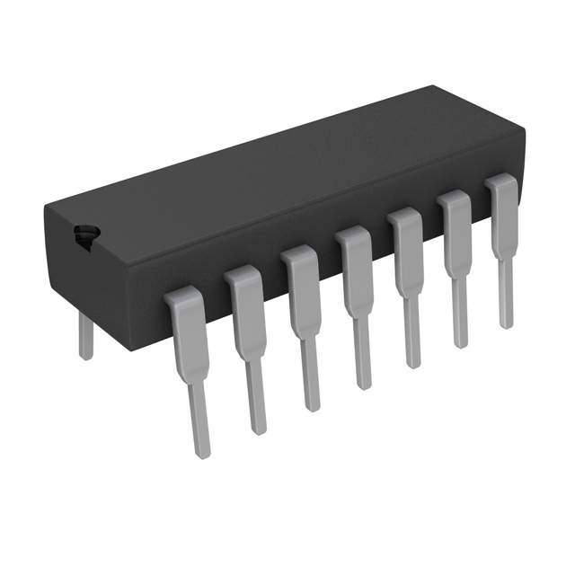
| 描述 | IC OPAMP GP 85KHZ 14DIP运算放大器 - 运放 Quad LiNCMOS |
| 产品分类 | Linear - Amplifiers - Instrumentation, OP Amps, Buffer Amps集成电路 - IC |
| 品牌 | Texas Instruments |
| 产品手册 | |
| 产品图片 |
|
| rohs | 符合RoHS无铅 / 符合限制有害物质指令(RoHS)规范要求 |
| 产品系列 | 放大器 IC,运算放大器 - 运放,Texas Instruments TLV2324INLinCMOS™ |
| 数据手册 | |
| 产品型号 | TLV2324IN |
| PCN设计/规格 | |
| 产品目录页面 | |
| 产品种类 | 运算放大器 - 运放 |
| 供应商器件封装 | 14-PDIP |
| 共模抑制比—最小值 | 65 dB |
| 关闭 | No Shutdown |
| 其它名称 | 296-7462-5 |
| 包装 | 管件 |
| 单位重量 | 1 g |
| 压摆率 | 0.03 V/µs |
| 商标 | Texas Instruments |
| 增益带宽生成 | 0.085 MHz |
| 增益带宽积 | 85kHz |
| 安装类型 | 通孔 |
| 安装风格 | Through Hole |
| 封装 | Tube |
| 封装/外壳 | 14-DIP(0.300",7.62mm) |
| 封装/箱体 | PDIP-14 |
| 工作温度 | -40°C ~ 85°C |
| 工作电源电压 | 2 V to 8 V |
| 工厂包装数量 | 25 |
| 技术 | LinCMOS |
| 放大器类型 | 通用 |
| 最大工作温度 | + 85 C |
| 最小工作温度 | - 40 C |
| 标准包装 | 25 |
| 电压-电源,单/双 (±) | 2 V ~ 8 V, ±1 V ~ 4 V |
| 电压-输入失调 | 1.1mV |
| 电流-电源 | 39µA |
| 电流-输入偏置 | 0.6pA |
| 电流-输出/通道 | 30mA |
| 电源电流 | 0.068 mA |
| 电路数 | 4 |
| 系列 | TLV2324 |
| 转换速度 | 0.03 V/us |
| 输入偏压电流—最大 | 2 nA |
| 输入参考电压噪声 | 68 nV |
| 输入补偿电压 | 10 mV |
| 输出电流 | 30 mA |
| 输出类型 | - |
| 通道数量 | 4 Channel |


- 商务部:美国ITC正式对集成电路等产品启动337调查
- 曝三星4nm工艺存在良率问题 高通将骁龙8 Gen1或转产台积电
- 太阳诱电将投资9.5亿元在常州建新厂生产MLCC 预计2023年完工
- 英特尔发布欧洲新工厂建设计划 深化IDM 2.0 战略
- 台积电先进制程称霸业界 有大客户加持明年业绩稳了
- 达到5530亿美元!SIA预计今年全球半导体销售额将创下新高
- 英特尔拟将自动驾驶子公司Mobileye上市 估值或超500亿美元
- 三星加码芯片和SET,合并消费电子和移动部门,撤换高东真等 CEO
- 三星电子宣布重大人事变动 还合并消费电子和移动部门
- 海关总署:前11个月进口集成电路产品价值2.52万亿元 增长14.8%


PDF Datasheet 数据手册内容提取
TLV2322, TLV2322Y, TLV2324, TLV2324Y LinCMOS LOW-VOLTAGE LOW-POWER OPERATIONAL AMPLIFIERS SLOS187 – FEBRUARY 1997 (cid:1) Wide Range of Supply Voltages Over TLV2322 Specified Temperature Range: D OR P PACKAGE T = –40°C to 85°C...2 V to 8 V (TOP VIEW) A (cid:1) Fully Characterized at 3 V and 5 V (cid:1) 1OUT 1 8 VDD Single-Supply Operation 1IN– 2 7 2OUT (cid:1) Common-Mode Input Voltage Range 1IN+ 3 6 2IN– Extends Below the Negative Rail and up to VDD–/GND 4 5 2IN+ VDD –1 V at TA = 25°C (cid:1) Output Voltage Range Includes Negative TLV2322 PW PACKAGE Rail (TOP VIEW) (cid:1) High Input Impedance...1012 W Typical (cid:1) ESD-Protection Circuitry 1OUT 1 8 VDD+ (cid:1) 1IN– 2 7 2OUT Designed-In Latch-Up Immunity 1IN+ 3 6 2IN– V /GND 4 5 2IN+ description DD– TLV2324 The TLV232x operational amplifiers are in a family D OR N PACKAGE of devices that has been specifically designed for (TOP VIEW) use in low-voltage single-supply applications. This amplifier is especially well suited to 1OUT 1 14 4OUT ultra-low-power systems that require devices to 1IN– 2 13 4IN– consume the absolute minimum of supply 1IN+ 3 12 4IN+ currents. Each amplifier is fully functional down to VDD+ 4 11 VDD–/GND a minimum supply voltage of 2 V, is fully 2IN+ 5 10 3IN+ characterized, tested, and specified at both 3-V 2IN– 6 9 3IN– and 5-V power supplies. The common-mode input 2OUT 7 8 3OUT voltage range includes the negative rail and extends to within 1 V of the positive rail. TLV2324 PW PACKAGE These amplifiers are specifically targeted for use (TOP VIEW) in very low-power, portable, battery-driven 1OUT 1 14 4OUT applications with the maximum supply current per 1IN– 4IN– operational amplifier specified at only 27 m A over 1IN+ 4IN+ its full temperature range of –40°C to 85°C. V V /GND DD+ DD– 2IN+ 3IN+ 2IN– 3IN– 2OUT 7 8 3OUT AVAILABLE OPTIONS PACKAGED DEVICES TA VVIO2mm5aa°Cxx AATT SMALL OUTLINE† PLASTIC DIP PLASTIC DIP TSSOP‡ CCHHIIPP( YFFOO) RRMM§§ (D) (N) (P) (PW) 9 mV TLV2322ID — TLV2322IP TLV2322IPWLE TLV2322Y –4400°°CC ttoo 8855°°CC 10 mV TLV2324ID TLV2324IN — TLV2324IPWLE TLV2324Y †The D package is available taped and reeled. Add R suffix to the device type (e.g., TLV2322IDR). ‡The PW package is only available left-end taped and reeled (e.g., TLV2322IPWLE). §Chip forms are tested at 25°C only. Please be aware that an important notice concerning availability, standard warranty, and use in critical applications of TexasInstruments semiconductor products and disclaimers thereto appears at the end of this data sheet. LinCMOS is a trademark of Texas Instruments Incorporated. PRODUCTION DATA information is current as of publication date. Copyright 1997, Texas Instruments Incorporated Products conform to specifications per the terms of Texas Instruments standard warranty. Production processing does not necessarily include testing of all parameters. POST OFFICE BOX 655303 • DALLAS, TEXAS 75265 1
TLV2322, TLV2322Y, TLV2324, TLV2324Y LinCMOS LOW-VOLTAGE LOW-POWER OPERATIONAL AMPLIFIERS SLOS187 – FEBRUARY 1997 description (continued) Low-voltage and low-power operation has been made possible by using the Texas Instruments silicon-gate LinCMOS technology. The LinCMOS process also features extremely high input impedance and ultra-low bias currents making these amplifiers ideal for interfacing to high-impedance sources such as sensor circuits or filter applications. To facilitate the design of small portable equipment, the TLV232x is made available in a wide range of package options, including the small-outline and thin-shrink small-outline packages (TSSOP). The TSSOP package has significantly reduced dimensions compared to a standard surface-mount package. Its maximum height of only 1.1 mm makes it particularly attractive when space is critical. The device inputs and outputs are designed to withstand –100-mA currents without sustaining latch-up. The TLV232x incorporates internal ESD-protection circuits that prevent functional failures at voltages up to 2000 V as tested under MIL-STD 883C, Method 3015.2; however, care should be exercised in handling these devices as exposure to ESD can result in the degradation of the device parametric performance. TLV2322Y chip information This chip, when properly assembled, displays characteristics similar to the TLV2322I. Thermal compression or ultrasonic bonding may be used on the doped-aluminum bonding pads. Chips may be mounted with conductive epoxy or a gold-silicon preform. BONDING PAD ASSIGNMENTS VDD (8) (5) (4) (3) (3) 1IN+ + (2) 1OUT 1IN– – (5) 2IN+ + (6) (2) (6) 2OUT 2IN– – 59 (4) VDD–/GND CHIP THICKNESS: 15 MILS TYPICAL BONDING PADS: 4 × 4 MILS MINIMUM (7) (1) (8) TJmax = 150°C TOLERANCES ARE ±10%. 72 ALL DIMENSIONS ARE IN MILS. 2 POST OFFICE BOX 655303 • DALLAS, TEXAS 75265
TLV2322, TLV2322Y, TLV2324, TLV2324Y LinCMOS LOW-VOLTAGE LOW-POWER OPERATIONAL AMPLIFIERS SLOS187 – FEBRUARY 1997 TLV2324Y chip information This chip, when properly assembled, display characteristics similar to the TLV2324. Thermal compression or ultrasonic bonding may be used on the doped-aluminum bonding pads. Chips may be mounted with conductive epoxy or a gold-silicon preform. BONDING PAD ASSIGNMENTS VDD (4) (3) (14) (13) (12) (11) (10) (9) (8) 1IN+ + (1) (2) 1OUT 1IN– – (5) 2IN+ + (7) (6) 2OUT 2IN– – 68 (10) 3IN+ + (8) (9) 3OUT 3IN– – (12) 4IN+ + (14) (1) (2) (3) (4) (5) (6) (7) (13) 4OUT 4IN– – 108 (11) VDD–/GND CHIP THICKNESS: 15 MILS TYPICAL BONDING PADS: 4 × 4 MILS MINIMUM TJmax = 150°C TOLERANCES ARE ±10%. ALL DIMENSIONS ARE IN MILS. PIN (12) IS INTERNALLY CONNECTED TO BACKSIDE OF CHIP. POST OFFICE BOX 655303 • DALLAS, TEXAS 75265 3
TLV2322, TLV2322Y, TLV2324, TLV2324Y LinCMOS LOW-VOLTAGE LOW-POWER OPERATIONAL AMPLIFIERS SLOS187 – FEBRUARY 1997 equivalent schematic (each amplifier) VDD P3 P4 R6 P1 P2 N5 IN– R1 R2 IN+ R5 C1 P5 P6 N3 OUT N4 N1 N2 N6 N7 R3 D1 R4 D2 R7 GND ACTUAL DEVICE COMPONENT COUNT† COMPONENT TLV2342 TLV2344 Transistors 54 108 Resistors 14 28 Diodes 4 8 Capacitors 2 4 †Includes both amplifiers and all ESD, bias, and trim circuitry. 4 POST OFFICE BOX 655303 • DALLAS, TEXAS 75265
TLV2322, TLV2322Y, TLV2324, TLV2324Y LinCMOS LOW-VOLTAGE LOW-POWER OPERATIONAL AMPLIFIERS SLOS187 – FEBRUARY 1997 absolute maximum ratings over operating free-air temperature (unless otherwise noted)† Supply voltage, V (see Note 1) . . . . . . . . . . . . . . . . . . . . . . . . . . . . . . . . . . . . . . . . . . . . . . . . . . . . . . . . . . . . . 8 V DD Differential input voltage, V (see Note 2) . . . . . . . . . . . . . . . . . . . . . . . . . . . . . . . . . . . . . . . . . . . . . . . . . . . V ± ID DD Input voltage range, V (any input) . . . . . . . . . . . . . . . . . . . . . . . . . . . . . . . . . . . . . . . . . . . . . . . . . . . –0.3 V to V I DD Input current, II . . . . . . . . . . . . . . . . . . . . . . . . . . . . . . . . . . . . . . . . . . . . . . . . . . . . . . . . . . . . . . . . . . . . . . . . . . ±5 mA Output current, I . . . . . . . . . . . . . . . . . . . . . . . . . . . . . . . . . . . . . . . . . . . . . . . . . . . . . . . . . . . . . . . . . . . . . . . ±30 mA O Duration of short-circuit current at (or below) T = 25°C (see Note 3) . . . . . . . . . . . . . . . . . . . . . . . . . unlimited A Continuous total dissipation . . . . . . . . . . . . . . . . . . . . . . . . . . . . . . . . . . . . . . . . . . . See Dissipation Rating Table Operating free-air temperature range, T . . . . . . . . . . . . . . . . . . . . . . . . . . . . . . . . . . . . . . . . . . . . –40°C to 85°C A Storage temperature range . . . . . . . . . . . . . . . . . . . . . . . . . . . . . . . . . . . . . . . . . . . . . . . . . . . . . . . . –65°C to 150°C Lead temperature 1,6 mm (1/16 inch) from case for 10 seconds . . . . . . . . . . . . . . . . . . . . . . . . . . . . . . . 260°C †Stresses beyond those listed under “absolute maximum ratings” may cause permanent damage to the device. These are stress ratings only, and functional operation of the device at these or any other conditions beyond those indicated under “recommended operating conditions” is not implied. Exposure to absolute-maximum rated conditions for extended periods may affect device reliability. NOTES: 1. All voltage values, except differential voltages, are with respect to network ground. 2. Differential voltages are at the noninverting input with respect to the inverting input. 3. The output may be shorted to either supply. Temperature and/or supply voltages must be limited to ensure that the maximum dissipation rating is not exceeded (see application section). DISSIPATION RATING TABLE TA ≤ 25°C DERATING FACTOR TA = 85°C PPAACCKKAAGGEE POWER RATING ABOVE TA = 25°C POWER RATING D–8 725 mW 5.8 mW/°C 377 mW D–14 950 mW 7.6 mW/°C 494 mW N 1575 mW 12.6 mW/°C 819 mW P 1000 mW 8.0 mW/°C 520 mW PW–8 525 mW 4.2 mW/°C 273 mW PW–14 700 mW 5.6 mW/°C 364 mW recommended operating conditions MIN MAX UNIT Supply voltage, VDD 2 8 V VDD = 3 V –0.2 1.8 CCoommmmoonn-mmooddee iinnppuutt vvoollttaaggee, VVIICC VV VDD = 5 V –0.2 3.8 Operating free-air temperature, TA –40 85 °C POST OFFICE BOX 655303 • DALLAS, TEXAS 75265 5
TLV2322, TLV2322Y, TLV2324, TLV2324Y LinCMOS LOW-VOLTAGE LOW-POWER OPERATIONAL AMPLIFIERS SLOS187 – FEBRUARY 1997 TLV2322 electrical characteristics at specified free-air temperature TLV2322 PARAMETER TEST CONDITIONS TAA†† VDD = 3 V VDD = 5 V UNIT MIN TYP MAX MIN TYP MAX VO = 1 V, 25°C 1.1 9 1.1 9 VIICC = 1 V,, VVIIOO IInnppuutt ooffffsseett vvoollttaaggee RS = 50 W, mmVV RL = 1 MW Full range 11 11 a VIO Aofv ienrpaugte o tfefsmept evoralttaugree coefficient 285°5C°C to 1 1.1 m V/°C IIIIOO IInnppuutt ooffffsseett ccuurrrreenntt ((sseeee NNoottee 44)) VOO = 1 V,, 25°C 0.1 0.1 ppAA VIC = 1 V 85°C 22 1000 24 1000 IIIIBB IInnppuutt bbiiaass ccuurrrreenntt ((sseeee NNoottee 44)) VOO = 1 V,, 25°C 0.6 0.6 ppAA VIC = 1 V 85°C 175 2000 200 2000 –0.2 –0.3 –0.2 –0.3 2255°°CC ttoo ttoo ttoo ttoo VV 2 2.3 4 4.2 Common-mode input voltagge VVIICCRR range (see Note 5) –0.2 –0.2 FFuullll rraannggee ttoo ttoo VV 1.8 3.8 VIC = 1 V, 25°C 1.75 1.9 3.2 3.8 VVOOHH HHiigghh-lleevveell oouuttppuutt vvoollttaaggee VVIIDD == 110000 mmVV, VV IOH = –1 mA Full range 1.7 3 VIC = 1 V, 25°C 115 150 95 150 VVOOLL LLooww-lleevveell oouuttppuutt vvoollttaaggee VVIIDD == – 110000 mmVV, mmVV IOL = 1 mA Full range 190 190 VIC = 1 V, 25°C 50 400 50 520 AAVVDD Largge-siggnal differential voltagge RRLL == 11 MMWW , VV//mmVV amplification See Note 6 Full range 50 50 VO = 1 V, 25°C 65 88 65 94 CCMMRRRR CCoommmmoonn-mmooddee rreejjeeccttiioonn rraattiioo VVIICC == VVIICCRRmmiinn, ddBB RS = 50 W Full range 60 60 VIC = 1 V, 25°C 70 86 70 86 Supplyy-voltagge rejjection ratio kkSSVVRR (D VDD/D VIO) RVVOOS === 5110 VV W, Full range 65 65 ddBB IIDDDD SSuuppppllyy ccuurrrreenntt VOO = 1 V,, VIICC = 1 V,, 25°C 12 34 20 34 mm AA No load Full range 54 54 †Full range is –40°C to 85°C. NOTES: 4. The typical values of input bias current and input offset current below 5 pA are determined mathematically. 5. This range also applies to each input individually. 6. At VDD = 5 V, VO(PP) = 0.25 V to 2 V; at VDD = 3 V, VO = 0.5 V to 1.5 6 POST OFFICE BOX 655303 • DALLAS, TEXAS 75265
TLV2322, TLV2322Y, TLV2324, TLV2324Y LinCMOS LOW-VOLTAGE LOW-POWER OPERATIONAL AMPLIFIERS SLOS187 – FEBRUARY 1997 TLV2322 operating characteristics at specified free-air temperature, V = 3 V DD TLV2322 PPAARRAAMMEETTEERR TTEESSTT CCOONNDDIITTIIOONNSS TTAA UUNNIITT MIN TYP MAX VIC = 1 V, VI(PP) = 1 V, 25°C 0.02 SSRR SSlleeww rraattee aatt uunniittyy ggaaiinn RRLL == 11 MMWW , CCLL == 2200 pFF, VV//mm ss SSee FFiigure 3355 8855°°CC 00.0022 Vn Equivalent input noise voltage f = 1 kHz, RS = 20 W , 25°C 68 nV/√Hz See Figure 36 BBOOMM MMaaxxiimmuumm oouuttppuutt-sswwiinngg bbaannddwwiiddtthh VROOL == 1V MOOHHW ,,, CSeLLe = F 2ig0u preF,, 35 2855°°CC 2.25 kkHHzz BB11 UUnniittyy-ggaaiinn bbaannddwwiiddtthh VRIIL = = 1 10 MmWV,,, CSeLLe = F 2ig0u preF,, 37 2855°°CC 2271 kkHHzz VVII = 1100 mmVV,, ff= BB11,, –40°C 39° f m Phase margin CL = 20 pF, RL = 1 MW , 25°C 34° See Figure 37 85°C 28° TLV2322 operating characteristics at specified free-air temperature, V = 5 V DD TLV2322 PPAARRAAMMEETTEERR TTEESSTT CCOONNDDIITTIIOONNSS TTAA UUNNIITT MIN TYP MAX 25°C 0.03 VVIICC == 11 VV, VVII((PPPP)) == 11 VV SSRR SSlleeww rraattee aatt uunniittyy ggaaiinn RLL = 1 MW ,, 85°C 0.03 VV//mm ss CL = 20 pF, 25°C 0.03 SSee FFiigure 3355 VVII((PPPP)) == 22.55 VV 85°C 0.02 Vn Equivalent input noise voltage f = 1 kHz, RS = 20 W , 25°C 68 nV/√Hz See Figure 36 BBOOMM MMaaxxiimmuumm oouuttppuutt-sswwiinngg bbaannddwwiiddtthh VROOL == 1V MOOHHW ,,, CSeLLe = F 2ig0u preF,, 35 2855°°CC 54 kkHHzz BB11 UUnniittyy-ggaaiinn bbaannddwwiiddtthh VRIIL = = 1 10 MmWV,,, CSeLLe = F 2ig0u preF,, 37 2855°°CC 8555 kkHHzz VVII = 1100 mmVV,, ff = BB11,, –40°C 38° f m Phase margin CL = 20 pF, RL = 1 MW , 25°C 34° See Figure 37 85°C 28° POST OFFICE BOX 655303 • DALLAS, TEXAS 75265 7
TLV2322, TLV2322Y, TLV2324, TLV2324Y LinCMOS LOW-VOLTAGE LOW-POWER OPERATIONAL AMPLIFIERS SLOS187 – FEBRUARY 1997 TLV2324I electrical characteristics at specified free-air temperature TLV2324I PARAMETER TEST CONDITIONS TAA†† VDD = 3 V VDD = 5 V UNIT MIN TYP MAX MIN TYP MAX VVOO = 11 VV,, 2255°°CC 11.11 1100 11.11 1100 VIICC = 1 V,, VVIIOO IInnppuutt ooffffsseett vvoollttaaggee RSS = 50 W, mmVV RL = 1 MW , FFuullll rraannggee 1122 1122 Averagge temperature coefficient 25°C to aa VVIIOO of input offset voltage 85°C 11 11.11 mm VV//°°CC IIIIOO IInnppuutt ooffffsseett ccuurrrreenntt ((sseeee NNoottee 44)) VOO = 1 V,, 25°C 0.1 0.1 ppAA VIC = 1 V 85°C 22 1000 24 1000 IIIIBB IInnppuutt bbiiaass ccuurrrreenntt ((sseeee NNoottee 44)) VOO = 1 V,, 25°C 0.6 0.6 ppAA VIC = 1 V 85°C 175 2000 200 2000 –0.2 –0.3 –0.2 –0.3 25°C to to to to V Common-mode input 2 2.3 4 4.2 VVIICCRR voltage range (see Note 5) –0.2 –0.2 Full rangge to to V 1.8 3.8 VVIICC == 11 VV, 2255°°CC 11.7755 11.99 33.22 33.88 VVOH HHiigghh-lleevveell oouuttppuutt vvoollttaaggee VVID = 110000 mmVV, VV IOH = –1 mA Full range 1.7 3 VVIICC == 11 VV, 2255°°CC 111155 115500 9955 115500 VVOL LLooww-lleevveell oouuttppuutt vvoollttaaggee VVID = –110000 mmVV, mmVV IOL = 1 mA Full range 190 190 Largge-siggnal differential VVIICC == 11 VV, 2255°°CC 5500 440000 5500 552200 AAVD voltage amplification RRL = 11 MMWW , VV//mmVV See Note 6 Full range 50 50 VVOO == 11 VV, 2255°°CC 6655 8888 6655 9944 CCMMRRRR CCoommmmoonn-mmooddee rreejjeeccttiioonn rraattiioo VVICC = VVICCRmmiinn, ddBB RS = 50 W Full range 60 60 SSuppllyy-vollttagge rejjjecttiion rattiio VVIICC = 11 VV, VVOO = 11 VV, 2255°°CC 7700 8866 7700 8866 kkSSVVRR (D VDD/D VIO) RS = 50 W Full range 65 65 ddBB IIDDDD SSuuppllyy ccuurrrreenntt VVOO = 11 VV, VVIICC = 11 VV, 2255°°CC 2244 6688 3399 6688 mm AA No load Full range 108 108 †Full range is –40°C to 85°C. NOTES: 4. The typical values of input bias current and input offset current below 5 pA are determined mathematically. 5. This range also applies to each input individually. 6. At VDD = 5 V, VO(PP) = 0.25 V to 2 V; at VDD = 3 V, VO = 0.5 V to 1.5 V. 8 POST OFFICE BOX 655303 • DALLAS, TEXAS 75265
TLV2322, TLV2322Y, TLV2324, TLV2324Y LinCMOS LOW-VOLTAGE LOW-POWER OPERATIONAL AMPLIFIERS SLOS187 – FEBRUARY 1997 TLV2324I operating characteristics at specified free-air temperature, V = 3 V DD TLV2324I PPAARRAAMMEETTEERR TTEESSTT CCOONNDDIITTIIOONNSS TTAA UUNNIITT MIN TYP MAX VVIICC == 11 VV, VVII((PPPP)) == 11 VV, 2255°°CC 00.0022 SSRR SSlleeww rraattee aatt uunniittyy ggaaiinn RRLL == 11 MMWW , CCLL == 2200 ppFF, VV//mm ss SSee FFiigure 3355 8855°°CC 00.0022 VVn EEqquuiivvaalleenntt iinnppuutt nnooiissee vvoollttaaggee f = 1 kHz,, RSS = 20 W ,, 2255°°CC 6688 nnVV√√//HHzz See Figure 36 BBOOMM MMaaxxiimmuumm oouuttppuutt-sswwiinngg bbaannddwwiiddtthh VROOL == 1V MOOHHW ,,, CSeLLe = F 2ig0u preF,, 35 2855°°CC 2.25 kkHHzz BB11 UUnniittyy-ggaaiinn bbaannddwwiiddtthh VRIIL = = 1 10 MmWV,,, CSeLLe = F 2ig0u preF,, 37 2855°°CC 2271 kkHHzz VVII = 1100 mmVV,, ff = BB11,, –40°C 39° f m Phase margin CL = 20 pF, RL = 1 MW , 25°C 34° See Figure 37 85°C 28° TLV2324I operating characteristics at specified free-air temperature, V = 5 V DD TLV2324I PPAARRAAMMEETTEERR TTEESSTT CCOONNDDIITTIIOONNSS TTAA UUNNIITT MIN TYP MAX 25°C 0.03 VVIICC == 11 VV, VVII((PPPP))== 11 VV SSRR SSlleeww rraattee aatt uunniittyy ggaaiinn RLL = 1 MW ,, 85°C 0.03 VV//mm ss CL = 20 pF, 25°C 0.03 SSee FFiigure 3355 VVII((PPPP)) == 22.55 VV 85°C 0.02 VVn EEqquuiivvaalleenntt iinnppuutt nnooiissee vvoollttaaggee f = 1 kHz,, RSS = 20 W ,, 2255°°CC 6688 nnVV//√√HHzz See Figure 36 BBOOMM MMaaxxiimmuumm oouuttppuutt-sswwiinngg bbaannddwwiiddtthh VROOL == 1V MOOHHW ,,, CSeLLe = F 2ig0u preF,, 35 2855°°CC 54 kkHHzz BB11 UUnniittyy-ggaaiinn bbaannddwwiiddtthh VRIIL = = 1 10 MmWV,,, CSeLLe = F 2ig0u preF,, 37 2855°°CC 8555 kkHHzz VVII = 1100 mmVV,, ff = BB11,, –40°C 38° f m Phase margin CL = 20 pF, RL = 1 MW , 25°C 34° See Figure 37 85°C 28° POST OFFICE BOX 655303 • DALLAS, TEXAS 75265 9
TLV2322, TLV2322Y, TLV2324, TLV2324Y LinCMOS LOW-VOLTAGE LOW-POWER OPERATIONAL AMPLIFIERS SLOS187 – FEBRUARY 1997 TLV2322Y electrical characteristics, TA = 25°C TLV2322Y PARAMETER TEST CONDITIONS VDD = 3 V VDD = 5 V UNIT MIN TYP MAX MIN TYP MAX VO = 1 V, VIC = 1 V, VIO Input offset voltage RS = 50 W , RL = 1 MW 1.1 1.1 mV IIO Input offset current (see Note 4) VO = 1 V, VIC = 1 V 0.1 0.1 pA IIB Input bias current (see Note 4) VO = 1 V, VIC = 1 V 0.6 0.6 pA –0.3 –0.3 Common-mode input voltage VICR to to V range (see Note 5) 2.3 4.2 VIC = 1 V, VID = –100 mV, VOH High-level output voltage 1.9 3.8 V IOH = –1 mA VIC = 1 V, VID = 100 mV, VOL Low-level output voltage 115 95 mV IOL = 1 mA Large-signal differential voltage VIC = 1 V, RL = 1 MW, AVD 400 520 V/mV amplification See Note 6 VO = 1 V, VIC = VICRmin, CMRR Common-mode rejection ratio 88 94 dB RS = 50 W Supply-voltage rejection ratio VO = 1 V, VIC = 1 V, kSVR (D VDD / D VID) RS = 50 W 86 86 dB IDD Supply current VO = 1 V, VIC = 1 V, 12 20 m A No load NOTES: 4. The typical values of input bias current offset current below 5 pA are determined mathematically. 5. This range also applies to each input individually. 6. At VDD = 5 V, VO = 0.25 V to 2 V; at VDD = 3 V, VO = 0.5 V to 1.5 V. 10 POST OFFICE BOX 655303 • DALLAS, TEXAS 75265
TLV2322, TLV2322Y, TLV2324, TLV2324Y LinCMOS LOW-VOLTAGE LOW-POWER OPERATIONAL AMPLIFIERS SLOS187 – FEBRUARY 1997 TLV2322Y electrical characteristics,TA = 25°C TLV2324Y PARAMETER TEST CONDITIONS VDD = 3 V VDD = 5 V UNIT MIN TYP MAX MIN TYP MAX VO = 1 V, VIC = 1 V, VIO Input offset voltage RS = 50 W , RL = 1 MW 1.1 1.1 mV IIO Input offset current (see Note 4) VO = 1 V, VIC = 1 V 0.1 0.1 pA IIB Input bias current (see Note 4) VO = 1 V, VIC = 1 V 0.6 0.6 pA –0.3 –0.3 Common-mode input voltage VICR range (see Note 5) to to V 2.3 4.2 VIC = 1 V, VID = 100 mV, VOH High-level output voltage IOH = –1 mA 1.9 3.8 V VIC = 1 V, VID = 100 mV, VOL Low-level output voltage IOL = 1 mA 115 95 mV Large-signal differential voltage VIC = 1 V, RL = 1 MW , AVD amplification See Note 6 400 520 V/mV VO = 1 V, VIC = VICRmin, CMRR Common-mode rejection ratio 88 94 dB RS = 50 W Supply-voltage rejection ratio VO = 1 V, VIC = 1 V, kSVR (D VDD/D VID) RS = 50 W 86 86 dB IDD Supply current VNOo l=o a1d V, VIC = 1 V, 24 39 m A NOTES: 4. The typical values of input bias current offset current below 5 pA are determined mathematically. 5. This range also applies to each input individually. 6. At VDD = 5 V, VO = 0.25 V to 2 V; at VDD = 3 V, VO = 0.5 V to 1.5 V. POST OFFICE BOX 655303 • DALLAS, TEXAS 75265 11
TLV2322, TLV2322Y, TLV2324, TLV2324Y LinCMOS LOW-VOLTAGE LOW-POWER OPERATIONAL AMPLIFIERS SLOS187 – FEBRUARY 1997 TYPICAL CHARACTERISTICS Table of Graphs FIGURE VIO Input offset voltage Distribution 1 – 4 a VIO Input offset voltage temperature coefficient Distribution 5 – 8 IIB Input bias current vs Free-air temperature 9 IIO Input offset current vs Free-air temperature 9 VIC Common-mode input voltage vs Supply voltage 10 vs High-level output current 11 VOH High-level output voltage vs Supply voltage 12 vs Free-air temperature 13 vs Common-mode input voltage 14 vs Free-air temperature 15, 16 VOL Low-level output voltage vs Differential input voltage 17 vs Low-level output current 18 vs Supply voltage 19 AVD Large-signal differential voltage amplification vs Free-air temperature 20 vs Frequency 21, 22 vs Supply voltage 23 IDD Supply current vs Free-air temperature 24, 25 vs Supply voltage 26 SR Slew rate vs Free-air temperature 27 VO(PP) Maximum peak-to-peak output voltage vs Frequency 28 vs Supply voltage 29 B1 Unity-gain bandwidth vs Free-air temperature 30 vs Supply voltage 31 f m Phase margin vs Free-air temperature 32 vs Load capacitance 33 Phase shift vs Frequency 21, 22 Vn Equivalent input noise voltage vs Frequency 34 12 POST OFFICE BOX 655303 • DALLAS, TEXAS 75265
TLV2322, TLV2322Y, TLV2324, TLV2324Y LinCMOS LOW-VOLTAGE LOW-POWER OPERATIONAL AMPLIFIERS SLOS187 – FEBRUARY 1997 TYPICAL CHARACTERISTICS DISTRIBUTION OF TLV2322 DISTRIBUTION OF TLV2322 INPUT OFFSET VOLTAGE INPUT OFFSET VOLTAGE 50 70 VDD = 5 V VTAD D= =25 3° CV 60 TPA P =a c2k5a°gCe 40 P Package % % 50 – – s s nit 30 nit U U 40 of of e e ag ag 30 nt 20 nt e e c c Per Per 20 10 10 0 0 –5 –4 –3 –2 –1 0 1 2 3 4 5 –5 –4 –3 –2 –1 0 1 2 3 4 5 VIO – Input Offset Voltage – mV VIO – Input Offset Voltage – mV Figure 1 Figure 2 DISTRIBUTION OF TLV2324 DISTRIBUTION OF TLV2324 INPUT OFFSET VOLTAGE INPUT OFFSET VOLTAGE 50 70 VDD = 3 V VDD = 5 V TA = 25°C TA = 25°C N Package 60 N Package 40 % % 50 – – s s nit 30 nit U U 40 of of e e ag ag 30 nt 20 nt e e c c r r Pe Pe 20 10 10 0 0 –5 –4 –3 –2 –1 0 1 2 3 4 5 –5 –4 –3 –2 –1 0 1 2 3 4 5 VIO – Input Offset Voltage – mV VIO – Input Offset Voltage – mV Figure 3 Figure 4 POST OFFICE BOX 655303 • DALLAS, TEXAS 75265 13
TLV2322, TLV2322Y, TLV2324, TLV2324Y LinCMOS LOW-VOLTAGE LOW-POWER OPERATIONAL AMPLIFIERS SLOS187 – FEBRUARY 1997 TYPICAL CHARACTERISTICS DISTRIBUTION OF TLV2322 DISTRIBUTION OF TLV2322 INPUT OFFSET VOLTAGE INPUT OFFSET VOLTAGE TEMPERATURE COEFFICIENT TEMPERATURE COEFFICIENT 50 70 VDD = 3 V VDD = 5 V TA = 25°C to 85°C TA = 25°C to 85°C P Package 60 P Package 40 Outliers: (1) 19.2 mV/°C – % – % 50 (1) 12.1 mV/°C s s nit 30 nit U U 40 of of e e ag ag 30 nt 20 nt e e c c Per Per 20 10 10 0 0 –10 –8 –6 –4 –2 0 2 4 6 8 10 –10 –8 –6 –4 –2 0 2 4 6 8 10 a VIO – Temperature Coefficient – m V/°C a VIO – Temperature Coefficient – m V/°C Figure 5 Figure 6 DISTRIBUTION OF TLV2324 DISTRIBUTION OF TLV2324 INPUT OFFSET VOLTAGE INPUT OFFSET VOLTAGE TEMPERATURE COEFFICIENT TEMPERATURE COEFFICIENT 50 70 VDD = 3 V VDD = 5 V TA = 25°C to 85°C TA = 25°C to 85°C N Package 60 N Package Outliers: (1) 19.2 mV/°C 40 (1) 12.1 mV/°C % % 50 Units – 30 Units – 40 of of ntage 20 ntage 30 Perce Perce 20 10 10 0 0 –10 –8 –6 –4 –2 0 2 4 6 8 10 –10 –8 –6 –4 –2 0 2 4 6 8 10 a VIO – Temperature Coefficient – m V/°C a VIO – Temperature Coefficient – m V/°C Figure 7 Figure 8 14 POST OFFICE BOX 655303 • DALLAS, TEXAS 75265
TLV2322, TLV2322Y, TLV2324, TLV2324Y LinCMOS LOW-VOLTAGE LOW-POWER OPERATIONAL AMPLIFIERS SLOS187 – FEBRUARY 1997 TYPICAL CHARACTERISTICS INPUT BIAS CURRENT AND INPUT OFFSET CURRENT COMMON-MODE INPUT VOLTAGE vs vs FREE-AIR TEMPERATURE SUPPLY VOLTAGE A 104 8 p rrents – 103 VVSDIeCeD =N = o1 3 tVe V A V TPAo s=it 2iv5e° CLimit et Cu ge – 6 s a nd Off 102 IIB ut Volt a p ut Bias 101 IIO Mode In 4 np n- – I mo O O m 2 d IIII 1 Co IIB anIIB VVIC – IC 0.1 0 25 45 65 85 105 125 0 2 4 6 8 TA – Free-Air Temperature – °C VDD – Supply Voltage – V NOTE A: The typical values of input bias current and input offset current below 5 pA were determined mathematically. Figure 9 Figure 10 HIGH-LEVEL OUTPUT VOLTAGE HIGH-LEVEL OUTPUT VOLTAGE vs vs HIGH-LEVEL OUTPUT CURRENT SUPPLY VOLTAGE 5 8 VIC = 1 V VIC = 1 V VID = 100 mV VID = 100 mV e – V 4 TA = 25°C e – V RTAL == 215 M°CW g g 6 a a olt olt ut V 3 VDD = 5 V ut V p p ut ut O O 4 el VDD = 3 V el v v e 2 e L L h- h- g g Hi Hi – – 2 H H 1 H H 0O 0O VV VV 0 0 0 – 2 – 4 –6 –8 0 2 4 6 8 IOH – High-Level Output Current – mA VDD – Supply Voltage – V Figure 11 Figure 12 POST OFFICE BOX 655303 • DALLAS, TEXAS 75265 15
TLV2322, TLV2322Y, TLV2324, TLV2324Y LinCMOS LOW-VOLTAGE LOW-POWER OPERATIONAL AMPLIFIERS SLOS187 – FEBRUARY 1997 TYPICAL CHARACTERISTICS HIGH-LEVEL OUTPUT VOLTAGE LOW-LEVEL OUTPUT VOLTAGE vs vs FREE-AIR TEMPERATURE COMMON-MODE INPUT VOLTAGE 3 700 VDD = 3 V VDD = 5 V V VIC = 1 V 650 IOL = 5 mA ge – 2.4 VID = 100 mV – mV 600 TA = 25°C ut Volta 1.8 Voltage 550 utp ut VID = –100 mV el O Outp 500 h-Lev 1.2 evel 450 Hig IOH = –500 m A w-L VV0H – OH 0.6 IIIIOOOOHHHH ==== ––––4321 mmmmAAAA OL – LoOL 430500 VID = –1 V VV 0 300 –75 –50 –25 0 25 50 75 100 125 0 0.5 1 1.5 2 2.5 3 3.5 4 TA – Free-Air Temperature – °C VIC – Common-Mode Input Voltage – V Figure 13 Figure 14 LOW-LEVEL OUTPUT VOLTAGE LOW-LEVEL OUTPUT VOLTAGE vs vs FREE-AIR TEMPERATURE FREE-AIR TEMPERATURE 900 200 VDD = 3 V VDD = 5 V V 185 VIC = 1 V V 800 VIC = 0.5 V e – m 170 VIOIDL == –1 1m0A0 mV e – m 700 VIOIDL == –5 1m VA g g a 155 a olt olt 600 V V put 140 put 500 Out 125 Out el el 400 ev 110 ev ow-L 95 ow-L 300 L L – – 200 L L 80 L L OO OO VV VV 100 65 50 0 –75 –50 –25 0 25 50 75 100 125 –75 –50 –25 0 25 50 75 100 125 TA – Free-Air Temperature – °C TA – Free-Air Temperature – °C Figure 15 Figure 16 16 POST OFFICE BOX 655303 • DALLAS, TEXAS 75265
TLV2322, TLV2322Y, TLV2324, TLV2324Y LinCMOS LOW-VOLTAGE LOW-POWER OPERATIONAL AMPLIFIERS SLOS187 – FEBRUARY 1997 TYPICAL CHARACTERISTICS LOW-LEVEL OUTPUT VOLTAGE LOW-LEVEL OUTPUT VOLTAGE vs vs DIFFERENTIAL INPUT VOLTAGE LOW-LEVEL OUTPUT CURRENT 800 1 VDD = 5 V VIC = 1 V V 700 VIC = |VID/2| 0.9 VID = –1 V ge – m 600 ITOAL = = 2 55 °mCA e – mV 0.8 TA = 25°C Volta 500 oltag 0.7 VDD = 5 V put ut V 0.6 Out 400 utp 0.5 vel el O Le 300 ev 0.4 VDD = 3 V ow- w-L 0.3 – L 200 Lo OL OL L – L 0.2 VV 100 OO VV 0.1 0 0 0 –1 –2 –3 –4 –5 –6 –7 –8 0 1 2 3 4 5 6 7 8 VID – Differential Input Voltage – V IOL – Low-Level Output Current – mA Figure 17 Figure 18 LARGE-SIGNAL LARGE-SIGNAL DIFFERENTIAL VOLTAGE AMPLIFICATION DIFFERENTIAL VOLTAGE AMPLIFICATION vs vs SUPPLY VOLTAGE FREE-AIR TEMPERATURE 2000 2000 RL = 1 MW RL = 1 MW – Large-Signal Differential VoltageDAmplification – V/mV 11111684084260000000000000000 TA = –4T0A° C= 25°C – Large-Signal Differential VoltageDAmplification – V/mV 11111684084260000000000000000 VDD = 3 V VDD = 5 V V V A A 200 200 TA = 85°C 0 0 0 2 4 6 8 –75 –50 –25 0 25 50 75 100 125 VDD – Supply Voltage – V TA – Free-Air Temperature – °C Figure 19 Figure 20 POST OFFICE BOX 655303 • DALLAS, TEXAS 75265 17
TLV2322, TLV2322Y, TLV2324, TLV2324Y LinCMOS LOW-VOLTAGE LOW-POWER OPERATIONAL AMPLIFIERS SLOS187 – FEBRUARY 1997 TYPICAL CHARACTERISTICS LARGE-SIGNAL DIFFERENTIAL VOLTAGE AMPLIFICATION AND PHASE SHIFT vs FREQUENCY 107 – 60° VDD = 3 V 106 RL = 1 MW – 30° CL = 20 pF TA = 25°C al 105 0° ntin eo e-Signal Differge Amplificati 111000432 AVD 369000°°° Phase Shift ga arolt Phase Shift LV – 101 120° D V A 1 150° 0.1 180° 1 10 100 1 k 10 k 100 k 1 M f – Frequency – Hz Figure 21 LARGE-SIGNAL DIFFERENTIAL VOLTAGE AMPLIFICATION AND PHASE SHIFT vs FREQUENCY 107 – 60° VDD = 5 V 106 RL = 1 MW – 30° CL = 20 pF TA = 25°C al 105 0° ntin eo e-Signal Differge Amplificati 111000432 AVD 369000°°° Phase Shift ga arolt Phase Shift LV – 101 120° D V A 1 150° 0.1 180° 1 10 100 1 k 10 k 100 k 1 M f – Frequency – Hz Figure 22 18 POST OFFICE BOX 655303 • DALLAS, TEXAS 75265
TLV2322, TLV2322Y, TLV2324, TLV2324Y LinCMOS LOW-VOLTAGE LOW-POWER OPERATIONAL AMPLIFIERS SLOS187 – FEBRUARY 1997 TYPICAL CHARACTERISTICS TLV2322 SUPPLY CURRENT SUPPLY CURRENT vs vs SUPPLY VOLTAGE FREE-AIR TEMPERATURE 45 35 VIC = 1 V 40 VO = 1 V VIC = 1 V No Load 30 VO = 1 V No Load AmA 35 AmA mCurrent – 3205 TA = –40°C TA = 25°C mCurrent – 2205 VDD = 5 V upply 20 upply 15 S S DD – DD 15 TA = 85°C DD – DD 10 VDD = 3 V II II 10 5 5 0 0 0 2 4 6 8 –75 –50 –25 0 25 50 75 100 125 VDD – Supply Voltage – V TA – Free-Air Temperature – °C Figure 23 Figure 24 TLV2324 SUPPLY CURRENT SLEW RATE vs vs FREE-AIR TEMPERATURE SUPPLY VOLTAGE 120 0.07 VIC = 1 V VIC = 1 V VO = 1 V VI(PP) = 1 V 0.06 100 No Load AV = 1 RL = 1 MW AmA 0.05 CL = 20 pF mnt – 80 mV/ussV/ TA = 25°C Curre 60 ate – 0.04 pply VDD = 5 V ew R 0.03 u Sl D – SD 40 SR – 0.02 DD II 20 VDD = 3 V 0.01 0 0 –75 –50 –25 0 25 50 75 100 125 0 2 4 6 8 TA – Free-Air Temperature – °C VDD – Supply Voltage – V Figure 25 Figure 26 POST OFFICE BOX 655303 • DALLAS, TEXAS 75265 19
TLV2322, TLV2322Y, TLV2324, TLV2324Y LinCMOS LOW-VOLTAGE LOW-POWER OPERATIONAL AMPLIFIERS SLOS187 – FEBRUARY 1997 TYPICAL CHARACTERISTICS SLEW RATE MAXIMUM PEAK-TO-PEAK OUTPUT VOLTAGE vs vs FREE-AIR TEMPERATURE FREQUENCY 0.07 V 5 0.06 VVAVIIC(P = =P 1 )1 = V 1 V oltage – VDD = 5 V 0.05 RCLL == 21 0M pWF put V 4 TA = –40°C ss ut u O mV/V/ k 3 TA = 25°C e – 0.04 Pea ew Rat 0.03 VDD = 5 V eak-to- 2 VDD = 3 V Sl P – m SR 0.02 VDD = 3 V mu Maxi 1 TA = 85°C 0.01 – P) RL = 1 MW P 0 O( 0 –75 –50 –25 0 25 50 75 100 125 V 0.1 1 10 100 TA – Free-Air Temperature – °C f – Frequency – kHz Figure 27 Figure 28 UNITY-GAIN BANDWIDTH UNITY-GAIN BANDWIDTH vs vs SUPPLY VOLTAGE FREE-AIR TEMPERATURE 120 140 VI = 10 mV Hz 110 RCLL == 21 0M pWF 125 RVIL = = 1 10 MmWV – M 100 TA = 25°C kHz 110 CL = 20 pF dth 90 h – dwi 80 widt 95 VDD = 5 V n Ban 70 Band 80 ai n y-G 60 Gai 65 Unit 50 nity- – U BB1 1 40 BB1 – 1 50 VDD = 3 V 35 30 20 20 0 1 2 3 4 5 6 7 8 –75 –50 –25 0 25 50 75 100 125 VDD – Supply Voltage – V TA – Free-Air Temperature – °C Figure 29 Figure 30 20 POST OFFICE BOX 655303 • DALLAS, TEXAS 75265
TLV2322, TLV2322Y, TLV2324, TLV2324Y LinCMOS LOW-VOLTAGE LOW-POWER OPERATIONAL AMPLIFIERS SLOS187 – FEBRUARY 1997 TYPICAL CHARACTERISTICS PHASE MARGIN PHASE MARGIN vs vs SUPPLY VOLTAGE FREE-AIR TEMPERATURE 42° 40° RVIL = = 1 10 MmWV 38° VDD = 3 V 40° CL = 20 pF TA = 25°C 36° VDD = 5 V Margin 38° Margin 3342°° om – Phase m 3364°° om – Phase m 322086°°° f f 24° 32° VI = 10 mV 22° RL = 1 MW CL = 20 pF 30° 20° 0 2 4 6 8 –75 –50 –25 0 25 50 75 100 125 VDD – Supply Voltage – V TA – Free-Air Temperature – °C Figure 31 Figure 32 PHASE MARGIN EQUIVALENT INPUT NOISE VOLTAGE vs vs LOAD CAPACITANCE FREQUENCY 40° 200 z 38° V HzV/H 175 VRDSD = =2 03 WV, 5 V 36° – nn TA = 25°C VDD = 3 V ge 150 34° a argin 32° e Volt 125 hase M 30° VDD = 5 V ut Nois 100 P p m – m 28° nt In 75 fo 26° ale v 50 24° qui VI = 10 mV E 22° RL = 1 MW n – n 25 TA = 25°C VV 20° 0 0 10 20 30 40 50 60 70 80 90 100 1 10 100 1000 CL – Load Capacitance – pF f – Frequency – Hz Figure 33 Figure 34 POST OFFICE BOX 655303 • DALLAS, TEXAS 75265 21
TLV2322, TLV2322Y, TLV2324, TLV2324Y LinCMOS LOW-VOLTAGE LOW-POWER OPERATIONAL AMPLIFIERS SLOS187 – FEBRUARY 1997 PARAMETER MEASUREMENT INFORMATION single-supply versus split-supply test circuits Because the TLV232x is optimized for single-supply operation, circuit configurations used for the various tests often present some inconvenience since the input signal, in many cases, must be offset from ground. This inconvenience can be avoided by testing the device with split supplies and the output load tied to the negative rail. A comparison of single-supply versus split-supply test circuits is shown below. The use of either circuit gives the same result. VDD VDD+ – – VO VO VI + VI + CL RL CL RL VDD– (a) SINGLE SUPPLY (b) SPLIT SUPPLY Figure 35. Unity-Gain Amplifier 2 kW 2 kW VDD VDD+ 20 W – – 1/2 VDD + VO + VO 20 W 20 W 20 W VDD– (a) SINGLE SUPPLY (b) SPLIT SUPPLY Figure 36. Noise-Test Circuits 10 kW 10 kW VDD VDD+ 100 W 100 W VI – VI – VO VO 1/2 VDD + + CL CL VDD– (a) SINGLE SUPPLY (b) SPLIT SUPPLY Figure 37. Gain-of-100 Inverting Amplifier 22 POST OFFICE BOX 655303 • DALLAS, TEXAS 75265
TLV2322, TLV2322Y, TLV2324, TLV2324Y LinCMOS LOW-VOLTAGE LOW-POWER OPERATIONAL AMPLIFIERS SLOS187 – FEBRUARY 1997 PARAMETER MEASUREMENT INFORMATION input bias current Because of the high input impedance of the TLV232x operational amplifier, attempts to measure the input bias current can result in erroneous readings. The bias current at normal ambient temperature is typically less than 1 pA, a value that is easily exceeded by leakages on the test socket. Two suggestions are offered to avoid erroneous measurements: • Isolate the device from other potential leakage sources. Use a grounded shield around and between the device inputs (see Figure 38). Leakages that would otherwise flow to the inputs are shunted away. • Compensate for the leakage of the test socket by actually performing an input bias current test (using a picoammeter) with no device in the test socket. The actual input bias current can then be calculated by subtracting the open-socket leakage readings from the readings obtained with a device in the test socket. Many automatic testers as well as some bench-top operational amplifier testers use the servo-loop technique with a resistor in series with the device input to measure the input bias current (the voltage drop across the series resistor is measured and the bias current is calculated). This method requires that a device be inserted into a test socket to obtain a correct reading; therefore, an open-socket reading is not feasible using this method. 8 5 V = VIC 1 4 Figure 38. Isolation Metal Around Device Inputs (P package) low-level output voltage To obtain low-level supply-voltage operation, some compromise is necessary in the input stage. This compromise results in the device low-level output voltage being dependent on both the common-mode input voltage level as well as the differential input voltage level. When attempting to correlate low-level output readings with those quoted in the electrical specifications, these two conditions should be observed. If conditions other than these are to be used, please refer to the Typical Characteristics section of this data sheet. input offset voltage temperature coefficient Erroneous readings often result from attempts to measure the temperature coefficient of input offset voltage. This parameter is actually a calculation using input offset voltage measurements obtained at two different temperatures. When one (or both) of the temperatures is below freezing, moisture can collect on both the device and the test socket. This moisture results in leakage and contact resistance that can cause erroneous input offset voltage readings. The isolation techniques previously mentioned have no effect on the leakage since the moisture also covers the isolation metal itself, thereby rendering it useless. These measurements should be performed at temperatures above freezing to minimize error. full-power response Full-power response, the frequency above which the operational amplifier slew rate limits the output voltage swing, is often specified two ways: full-linear response and full-peak response. The full-linear response is POST OFFICE BOX 655303 • DALLAS, TEXAS 75265 23
TLV2322, TLV2322Y, TLV2324, TLV2324Y LinCMOS LOW-VOLTAGE LOW-POWER OPERATIONAL AMPLIFIERS SLOS187 – FEBRUARY 1997 PARAMETER MEASUREMENT INFORMATION generally measured by monitoring the distortion level of the output while increasing the frequency of a sinusoidal input signal until the maximum frequency is found above which the output contains significant distortion. The full-peak response is defined as the maximum output frequency, without regard to distortion, above which full peak-to-peak output swing cannot be maintained. Because there is no industry-wide accepted value for significant distortion, the full-peak response is specified in this data sheet and is measured using the circuit of Figure 35. The initial setup involves the use of a sinusoidal input to determine the maximum peak-to-peak output of the device (the amplitude of the sinusoidal wave is increased until clipping occurs). The sinusoidal wave is then replaced with a square wave of the same amplitude. The frequency is then increased until the maximum peak-to-peak output can no longer be maintained (Figure 39). A square wave is used to allow a more accurate determination of the point at which the maximum peak-to-peak output is reached. (a) f = 100 Hz (d) BOM > f > 100 Hz (d) f = BOM (d) f > BOM Figure 39. Full-Power-Response Output Signal test time Inadequate test time is a frequent problem, especially when testing CMOS devices in a high-volume, short-test-time environment. Internal capacitances are inherently higher in CMOS than in bipolar and BiFET devices and require longer test times than their bipolar and BiFET counterparts. The problem becomes more pronounced with reduced supply levels and lower temperatures. APPLICATION INFORMATION single-supply operation VDD While the TLV232x performs well using dual- R2 power supplies (also called balanced or split supplies), the design is optimized for single- supply operation. This includes an input common- mode voltage range that encompasses ground as R1 well as an output voltage range that pulls down to VI – ground. The supply voltage range extends down VO TLE2426 + to 2 V, thus allowing operation with supply levels commonly available for TTL and HCMOS. VO(cid:2)(cid:3)VDD2–VI(cid:4) RR21 (cid:1)VD2D Many single-supply applications require that a voltage be applied to one input to establish a reference level that is above ground. This virtual Figure 40. Inverting Amplifier With Voltage ground can be generated using two large Reference resistors, but a preferred technique is to use a virtual-ground generator such as the TLE2426 (see Figure 40). The TLE2426 supplies an accurate voltage equal to V /2, while consuming very little power and is suitable for supply voltages of greater than 4 V. DD 24 POST OFFICE BOX 655303 • DALLAS, TEXAS 75265
TLV2322, TLV2322Y, TLV2324, TLV2324Y LinCMOS LOW-VOLTAGE LOW-POWER OPERATIONAL AMPLIFIERS SLOS187 – FEBRUARY 1997 APPLICATION INFORMATION single-supply operation (continued) The TLV232x works well in conjunction with digital logic; however, when powering both linear devices and digital logic from the same power supply, the following precautions are recommended: • Power the linear devices from separate bypassed supply lines (see Figure 41); otherwise, the linear device supply rails can fluctuate due to voltage drops caused by high switching currents in the digital logic. • Use proper bypass techniques to reduce the probability of noise-induced errors. Single capacitive decoupling is often adequate; however, RC decoupling may be necessary in high-frequency applications. – Power Logic Logic Logic + Supply (a) COMMON-SUPPLY RAILS – Power Logic Logic Logic + Supply (b) SEPARATE-BYPASSED SUPPLY RAILS (preferred) Figure 41. Common Versus Separate Supply Rails input characteristics The TLV232x is specified with a minimum and a maximum input voltage that, if exceeded at either input, could cause the device to malfunction. Exceeding this specified range is a common problem, especially in single-supply operation. The lower the range limit includes the negative rail, while the upper range limit is specified at V – 1 V at T = 25°C and at V – 1.2 V at all other temperatures. DD A DD The use of the polysilicon-gate process and the careful input circuit design gives the TLV232x very good input offset voltage drift characteristics relative to conventional metal-gate processes. Offset voltage drift in CMOS devices is highly influenced by threshold voltage shifts caused by polarization of the phosphorus dopant implanted in the oxide. Placing the phosphorus dopant in a conductor (such as a polysilicon gate) alleviates the polarization problem, thus reducing threshold voltage shifts by more than an order of magnitude. The offset voltage drift with time has been calculated to be typically 0.1 m V/month, including the first month of operation. Because of the extremely high input impedance and resulting low bias-current requirements, the TLV232x is well suited for low-level signal processing; however, leakage currents on printed-circuit boards and sockets can easily exceed bias-current requirements and cause a degradation in device performance. It is good practice to include guard rings around inputs (similar to those of Figure 38 in the Parameter Measurement Information section). These guards should be driven from a low-impedance source at the same voltage level as the common-mode input (see Figure 42). The inputs of any unused amplifiers should be tied to ground to avoid possible oscillation. POST OFFICE BOX 655303 • DALLAS, TEXAS 75265 25
TLV2322, TLV2322Y, TLV2324, TLV2324Y LinCMOS LOW-VOLTAGE LOW-POWER OPERATIONAL AMPLIFIERS SLOS187 – FEBRUARY 1997 APPLICATION INFORMATION input characteristics (continued) – VI – – VO VO VO Vi + + VI + (a) NONINVERTING AMPLIFIER (b) INVERTING AMPLIFIER (c) UNITY-GAIN AMPLIFIER Figure 42. Guard-Ring Schemes noise performance The noise specifications in operational amplifier circuits are greatly dependent on the current in the first-stage differential amplifier. The low input bias-current requirements of the TLV232x result in a very low noise current, which is insignificant in most applications. This feature makes the device especially favorable over bipolar devices when using values of circuit impedance greater than 50 kW , since bipolar devices exhibit greater noise currents. feedback Operational amplifier circuits nearly always employ feedback, and since feedback is the first prerequisite for oscillation, caution is appropriate. Most oscillation problems result from driving capacitive loads and ignoring stray input – capacitance. A small-value capacitor connected + in parallel with the feedback resistor is an effective remedy (see Figure 43). The value of this capacitor is optimized empirically. electrostatic-discharge protection Figure 43. Compensation for Input Capacitance The TLV232x incorporates an internal electrostatic-discharge (ESD)-protection circuit that prevents functional failures at voltages up to 2000 V as tested under MIL-PRF-38535, Method 3015.2. Care should be exercised, however, when handling these devices as exposure to ESD can result in the degradation of the device parametric performance. The protection circuit also causes the input bias currents to be temperature dependent and have the characteristics of a reverse-biased diode. latch-up Because CMOS devices are susceptible to latch-up due to their inherent parasitic thyristors, the TLV232x inputs and outputs are designed to withstand –100-mA surge currents without sustaining latch-up; however, techniques should be used to reduce the chance of latch-up whenever possible. Internal-protection diodes should not by design be forward biased. Applied input and output voltage should not exceed the supply voltage 26 POST OFFICE BOX 655303 • DALLAS, TEXAS 75265
TLV2322, TLV2322Y, TLV2324, TLV2324Y LinCMOS LOW-VOLTAGE LOW-POWER OPERATIONAL AMPLIFIERS SLOS187 – FEBRUARY 1997 APPLICATION INFORMATION by more than 300 mV. Care should be exercised when using capacitive coupling on pulse generators. Supply transients should be shunted by the use of decoupling capacitors (0.1 m F typical) located across the supply rails as close to the device as possible. The current path established if latch-up occurs is usually between the positive supply rail and ground and can be triggered by surges on the supply lines and/or voltages on either the output or inputs that exceed the supply voltage. Once latch-up occurs, the current flow is limited only by the impedance of the power supply and the forward resistance of the parasitic thyristor and usually results in the destruction of the device. The chance of latch-up occurring increases with increasing temperature and supply voltages. output characteristics VDD The output stage of the TLV232x is designed to sink and source relatively high amounts of current (ssuebeje cTtyepdi catlo Chaa raschtoerrti-sctiirccsu)i.t Ifc othned itoiount,p utt hiiss VI – IP RP RP(cid:3)IVD(cid:1)DI(cid:2)(cid:1)VOI + F L P high-current capability can cause device damage VO under certain conditions. Output current capability IF IP = Pullup Current Required by the increases with supply voltage. Operational Amplifier Although the TLV232x possesses excellent R2 (typically 500 m A) R1 IL RL high-level output voltage and current capability, methods are available for boosting this capability, if needed. The simplest method involves the use of a pullup resistor (R ) connected from the output P Figure 44. Resistive Pullup to Increase V to the positive supply rail (see Figure 44). There OH are two disadvantages to the use of this circuit. First, the NMOS pulldown transistor N4 (see equivalent schematic) must sink a comparatively 2.5 V large amount of current. In this circuit, N4 behaves like a linear resistor with an on resistance between – approximately 60 W and 180 W depending on how VO VI + hard the operational amplifier input is driven. With very low values of RP, a voltage offset from 0 V at CL the output occurs. Secondly, pullup resistor R P acts as a drain load to N4 and the gain of the TA = 25°C operational amplifier is reduced at output voltage f = 1 kHz levels where N5 is not supplying the output VI(PP) = 1 V –2.5 V current. Figure 45. Test Circuit for Output Characteristics All operating characteristics of the TLV232x are measured using a 20-pF load. The device drives higher capacitive loads; however, as output load capacitance increases, the resulting response pole occurs at lower frequencies, thereby causing ringing, peaking, or even oscillation (see Figure 45 and Figure 46). In many cases, adding some compensation in the form of a series resistor in the feedback loop alleviates the problem. POST OFFICE BOX 655303 • DALLAS, TEXAS 75265 27
TLV2322, TLV2322Y, TLV2324, TLV2324Y LinCMOS LOW-VOLTAGE LOW-POWER OPERATIONAL AMPLIFIERS SLOS187 – FEBRUARY 1997 APPLICATION INFORMATION output characteristics (continued) (a) CL = 20 pF, RL = NO LOAD (b) CL = 260 pF, RL = NO LOAD (c) CL = 310 pF, RL = NO LOAD Figure 46. Effect of Capacitive Loads 28 POST OFFICE BOX 655303 • DALLAS, TEXAS 75265
PACKAGE OPTION ADDENDUM www.ti.com 6-Feb-2020 PACKAGING INFORMATION Orderable Device Status Package Type Package Pins Package Eco Plan Lead/Ball Finish MSL Peak Temp Op Temp (°C) Device Marking Samples (1) Drawing Qty (2) (6) (3) (4/5) TLV2322ID ACTIVE SOIC D 8 75 Green (RoHS NIPDAU Level-1-260C-UNLIM -40 to 85 2322I & no Sb/Br) TLV2322IDR ACTIVE SOIC D 8 2500 Green (RoHS NIPDAU Level-1-260C-UNLIM -40 to 85 2322I & no Sb/Br) TLV2322IP ACTIVE PDIP P 8 50 Green (RoHS NIPDAU N / A for Pkg Type -40 to 85 TLV2322IP & no Sb/Br) TLV2322IPW ACTIVE TSSOP PW 8 150 Green (RoHS NIPDAU Level-1-260C-UNLIM -40 to 85 TY2322 & no Sb/Br) TLV2322IPWR ACTIVE TSSOP PW 8 2000 Green (RoHS NIPDAU Level-1-260C-UNLIM -40 to 85 TY2322 & no Sb/Br) TLV2324ID ACTIVE SOIC D 14 50 Green (RoHS NIPDAU Level-1-260C-UNLIM -40 to 85 TLV2324I & no Sb/Br) TLV2324IDR ACTIVE SOIC D 14 2500 Green (RoHS NIPDAU Level-1-260C-UNLIM -40 to 85 TLV2324I & no Sb/Br) TLV2324IN ACTIVE PDIP N 14 25 Green (RoHS NIPDAU N / A for Pkg Type -40 to 85 TLV2324IN & no Sb/Br) TLV2324IPWR ACTIVE TSSOP PW 14 2000 Green (RoHS NIPDAU Level-1-260C-UNLIM -40 to 85 TY2324 & no Sb/Br) (1) The marketing status values are defined as follows: ACTIVE: Product device recommended for new designs. LIFEBUY: TI has announced that the device will be discontinued, and a lifetime-buy period is in effect. NRND: Not recommended for new designs. Device is in production to support existing customers, but TI does not recommend using this part in a new design. PREVIEW: Device has been announced but is not in production. Samples may or may not be available. OBSOLETE: TI has discontinued the production of the device. (2) RoHS: TI defines "RoHS" to mean semiconductor products that are compliant with the current EU RoHS requirements for all 10 RoHS substances, including the requirement that RoHS substance do not exceed 0.1% by weight in homogeneous materials. Where designed to be soldered at high temperatures, "RoHS" products are suitable for use in specified lead-free processes. TI may reference these types of products as "Pb-Free". RoHS Exempt: TI defines "RoHS Exempt" to mean products that contain lead but are compliant with EU RoHS pursuant to a specific EU RoHS exemption. Green: TI defines "Green" to mean the content of Chlorine (Cl) and Bromine (Br) based flame retardants meet JS709B low halogen requirements of <=1000ppm threshold. Antimony trioxide based flame retardants must also meet the <=1000ppm threshold requirement. (3) MSL, Peak Temp. - The Moisture Sensitivity Level rating according to the JEDEC industry standard classifications, and peak solder temperature. Addendum-Page 1
PACKAGE OPTION ADDENDUM www.ti.com 6-Feb-2020 (4) There may be additional marking, which relates to the logo, the lot trace code information, or the environmental category on the device. (5) Multiple Device Markings will be inside parentheses. Only one Device Marking contained in parentheses and separated by a "~" will appear on a device. If a line is indented then it is a continuation of the previous line and the two combined represent the entire Device Marking for that device. (6) Lead/Ball Finish - Orderable Devices may have multiple material finish options. Finish options are separated by a vertical ruled line. Lead/Ball Finish values may wrap to two lines if the finish value exceeds the maximum column width. Important Information and Disclaimer:The information provided on this page represents TI's knowledge and belief as of the date that it is provided. TI bases its knowledge and belief on information provided by third parties, and makes no representation or warranty as to the accuracy of such information. Efforts are underway to better integrate information from third parties. TI has taken and continues to take reasonable steps to provide representative and accurate information but may not have conducted destructive testing or chemical analysis on incoming materials and chemicals. TI and TI suppliers consider certain information to be proprietary, and thus CAS numbers and other limited information may not be available for release. In no event shall TI's liability arising out of such information exceed the total purchase price of the TI part(s) at issue in this document sold by TI to Customer on an annual basis. Addendum-Page 2
PACKAGE MATERIALS INFORMATION www.ti.com 26-Feb-2019 TAPE AND REEL INFORMATION *Alldimensionsarenominal Device Package Package Pins SPQ Reel Reel A0 B0 K0 P1 W Pin1 Type Drawing Diameter Width (mm) (mm) (mm) (mm) (mm) Quadrant (mm) W1(mm) TLV2322IDR SOIC D 8 2500 330.0 12.4 6.4 5.2 2.1 8.0 12.0 Q1 TLV2322IPWR TSSOP PW 8 2000 330.0 12.4 7.0 3.6 1.6 8.0 12.0 Q1 TLV2324IDR SOIC D 14 2500 330.0 16.4 6.5 9.0 2.1 8.0 16.0 Q1 TLV2324IPWR TSSOP PW 14 2000 330.0 12.4 6.9 5.6 1.6 8.0 12.0 Q1 PackMaterials-Page1
PACKAGE MATERIALS INFORMATION www.ti.com 26-Feb-2019 *Alldimensionsarenominal Device PackageType PackageDrawing Pins SPQ Length(mm) Width(mm) Height(mm) TLV2322IDR SOIC D 8 2500 340.5 338.1 20.6 TLV2322IPWR TSSOP PW 8 2000 367.0 367.0 35.0 TLV2324IDR SOIC D 14 2500 350.0 350.0 43.0 TLV2324IPWR TSSOP PW 14 2000 367.0 367.0 35.0 PackMaterials-Page2
IMPORTANTNOTICEANDDISCLAIMER TI PROVIDES TECHNICAL AND RELIABILITY DATA (INCLUDING DATASHEETS), DESIGN RESOURCES (INCLUDING REFERENCE DESIGNS), APPLICATION OR OTHER DESIGN ADVICE, WEB TOOLS, SAFETY INFORMATION, AND OTHER RESOURCES “AS IS” AND WITH ALL FAULTS, AND DISCLAIMS ALL WARRANTIES, EXPRESS AND IMPLIED, INCLUDING WITHOUT LIMITATION ANY IMPLIED WARRANTIES OF MERCHANTABILITY, FITNESS FOR A PARTICULAR PURPOSE OR NON-INFRINGEMENT OF THIRD PARTY INTELLECTUAL PROPERTY RIGHTS. These resources are intended for skilled developers designing with TI products. You are solely responsible for (1) selecting the appropriate TI products for your application, (2) designing, validating and testing your application, and (3) ensuring your application meets applicable standards, and any other safety, security, or other requirements. These resources are subject to change without notice. TI grants you permission to use these resources only for development of an application that uses the TI products described in the resource. Other reproduction and display of these resources is prohibited. No license is granted to any other TI intellectual property right or to any third party intellectual property right. TI disclaims responsibility for, and you will fully indemnify TI and its representatives against, any claims, damages, costs, losses, and liabilities arising out of your use of these resources. TI’s products are provided subject to TI’s Terms of Sale (www.ti.com/legal/termsofsale.html) or other applicable terms available either on ti.com or provided in conjunction with such TI products. TI’s provision of these resources does not expand or otherwise alter TI’s applicable warranties or warranty disclaimers for TI products. Mailing Address: Texas Instruments, Post Office Box 655303, Dallas, Texas 75265 Copyright © 2020, Texas Instruments Incorporated