ICGOO在线商城 > TLE4921-5U
 Datasheet下载
- 型号: TLE4921-5U
- 制造商: Infineon
- 库位|库存: xxxx|xxxx
- 要求:
| 数量阶梯 | 香港交货 | 国内含税 |
| +xxxx | $xxxx | ¥xxxx |
查看当月历史价格
查看今年历史价格
TLE4921-5U产品简介:
ICGOO电子元器件商城为您提供TLE4921-5U由Infineon设计生产,在icgoo商城现货销售,并且可以通过原厂、代理商等渠道进行代购。 提供TLE4921-5U价格参考以及InfineonTLE4921-5U封装/规格参数等产品信息。 你可以下载TLE4921-5U参考资料、Datasheet数据手册功能说明书, 资料中有TLE4921-5U详细功能的应用电路图电压和使用方法及教程。
| 参数 | 数值 |
| 产品目录 | |
| 描述 | IC HALL EFFECT SENSOR SSO-4-1板机接口霍耳效应/磁性传感器 Differential 4.5V - 24V 8.8 mA |
| 产品分类 | 磁性传感器 - 霍尔效应,数字开关,线性,罗盘 (IC)磁性传感器 |
| 品牌 | Infineon Technologies |
| 产品手册 | |
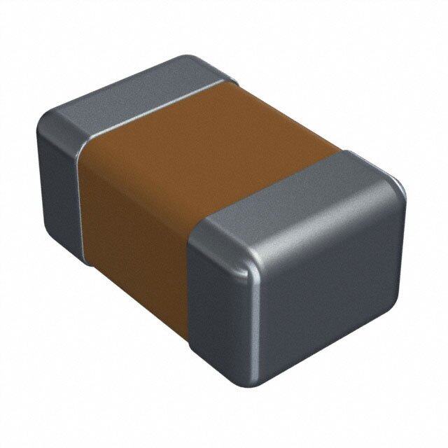
| 产品图片 |
|
| rohs | 符合RoHS无铅 / 符合限制有害物质指令(RoHS)规范要求 |
| 产品系列 | 板机接口霍耳效应/磁性传感器,Infineon Technologies TLE4921-5U- |
| 数据手册 | http://www.infineon.com/dgdl/TLE4921-5U_V1.1.pdf?folderId=db3a30431689f4420116a096e1db033e&fileId=db3a304319c6f18c011a2a97e3a612d8 |
| 产品型号 | TLE4921-5U |
| 产品种类 | 板机接口霍耳效应/磁性传感器 |
| 供应商器件封装 | P-SSO-4-1 |
| 其它名称 | TLE4921-5UINCT |
| 包装 | 剪切带 (CT) |
| 商标 | Infineon Technologies |
| 安装风格 | Through Hole |
| 封装 | Ammo Pack |
| 封装/外壳 | 4-SIP,SSO-4-01 |
| 封装/箱体 | SSO-4 |
| 工作温度 | -40°C ~ 170°C |
| 工作电源电压 | 5 V or 9 V or 12 V |
| 工厂包装数量 | 2000 |
| 感应范围 | 0mT 跳闸,0mT 释放 |
| 最大工作温度 | + 170 C |
| 最大输出电流 | 50 mA |
| 最小工作温度 | - 40 C |
| 标准包装 | 1 |
| 特性 | 高灵敏度 |
| 电压-电源 | 4.5 V ~ 24 V |
| 电流-电源 | 5.3mA |
| 电流-输出(最大值) | 50mA |
| 类型 | |
| 系列 | TLE4921 |
| 输出类型 | 数字式,差分 |
| 零件号别名 | SP000013593 TLE49215UHALA1 |


- 商务部:美国ITC正式对集成电路等产品启动337调查
- 曝三星4nm工艺存在良率问题 高通将骁龙8 Gen1或转产台积电
- 太阳诱电将投资9.5亿元在常州建新厂生产MLCC 预计2023年完工
- 英特尔发布欧洲新工厂建设计划 深化IDM 2.0 战略
- 台积电先进制程称霸业界 有大客户加持明年业绩稳了
- 达到5530亿美元!SIA预计今年全球半导体销售额将创下新高
- 英特尔拟将自动驾驶子公司Mobileye上市 估值或超500亿美元
- 三星加码芯片和SET,合并消费电子和移动部门,撤换高东真等 CEO
- 三星电子宣布重大人事变动 还合并消费电子和移动部门
- 海关总署:前11个月进口集成电路产品价值2.52万亿元 增长14.8%


PDF Datasheet 数据手册内容提取
Data Sheet, V 1.1, January 2008 T L E 4 9 2 1 - 5 U Dynamic Differential Hall Effect Sensor IC Sensors N e v e r s t o p t h i n k i n g .
Edition 2008-01 Published by Infineon Technologies AG, St.-Martin-Strasse 53, 81669 München, Germany © Infineon Technologies AG 2008. All Rights Reserved. Attention please! The information herein is given to describe certain components and shall not be considered as a guarantee of characteristics. Terms of delivery and rights to technical change reserved. We hereby disclaim any and all warranties, including but not limited to warranties of non-infringement, regarding circuits, descriptions and charts stated herein. Information For further information on technology, delivery terms and conditions and prices please contact your nearest Infineon Technologies Office (www.infineon.com). Warnings Due to technical requirements components may contain dangerous substances. For information on the types in question please contact your nearest Infineon Technologies Office. Infineon Technologies Components may only be used in life-support devices or systems with the express written approval of Infineon Technologies, if a failure of such components can reasonably be expected to cause the failure of that life-support device or system, or to affect the safety or effectiveness of that device or system. Life support devices or systems are intended to be implanted in the human body, or to support and/or maintain and sustain and/or protect human life. If they fail, it is reasonable to assume that the health of the user or other persons may be endangered.
TLE4921-5U Revision History: 2008-01 V 1.1 Previous Version: V1.0 Page Subjects (major changes since last revision) 5 Ordering Code changed 11 “Output leakage current” unit corrected 20 Figures “Delay Time between Switching Threshold” exchanged and corrected 21 Figure “Delay Time versus Differential Field” corrected We Listen to Your Comments Any information within this document that you feel is wrong, unclear or missing at all? Your feedback will help us to continuously improve the quality of this document. Please send your proposal (including a reference to this document) to: sensors@infineon.com Template: mc_a5_ds_tmplt.fm / 4 / 2004-09-15
TLE4921-5U Table of Contents Page 1 Overview . . . . . . . . . . . . . . . . . . . . . . . . . . . . . . . . . . . . . . . . . . . . . . . . . . . 5 1.1 Features . . . . . . . . . . . . . . . . . . . . . . . . . . . . . . . . . . . . . . . . . . . . . . . . . . . . 5 1.2 Pin Configuration (view on branded side of component) . . . . . . . . . . . . . . . . . . . . . . . . . . . . . 6 2 General . . . . . . . . . . . . . . . . . . . . . . . . . . . . . . . . . . . . . . . . . . . . . . . . . . . . 7 2.1 Block Diagram . . . . . . . . . . . . . . . . . . . . . . . . . . . . . . . . . . . . . . . . . . . . . . . 7 2.2 Functional Description . . . . . . . . . . . . . . . . . . . . . . . . . . . . . . . . . . . . . . . . . 8 2.3 Circuit Description (see Figure 2) . . . . . . . . . . . . . . . . . . . . . . . . . . . . . . . . 8 3 Maximum Ratings . . . . . . . . . . . . . . . . . . . . . . . . . . . . . . . . . . . . . . . . . . . 9 4 Operating Range . . . . . . . . . . . . . . . . . . . . . . . . . . . . . . . . . . . . . . . . . . . 10 5 Electrical and Magnetic Parameters . . . . . . . . . . . . . . . . . . . . . . . . . . . 11 6 Application Configurations . . . . . . . . . . . . . . . . . . . . . . . . . . . . . . . . . . . 14 7 Typical Performance Characteristics . . . . . . . . . . . . . . . . . . . . . . . . . . 18 8 Package Outlines . . . . . . . . . . . . . . . . . . . . . . . . . . . . . . . . . . . . . . . . . . . 25 Data Sheet 4 V 1.1, 2008-01
Dynamic Differential Hall Effect Sensor IC TLE4921-5U Bipolar IC 1 Overview 1.1 Features • Advanced performance • High sensitivity • Symmetrical thresholds • High piezo resistivity • Reduced power consumption • South and north pole pre-induction possible • AC coupled • Digital output signal • Two-wire and three-wire configuration possible • Large temperature range • Large airgap • Low cut-off frequency • Protection against overvoltage • Protection against reversed polarity • Output protection against electrical disturbances The differential Hall Effect sensor TLE4921-5U provides a high sensitivity and a superior stability over temperature and symmetrical thresholds in order to achieve a stable duty cycle. TLE4921-5U is particularly suitable for rotational speed detection and timing applications of ferromagnetic toothed wheels such as anti-lock braking systems, transmissions, crankshafts, etc. The integrated circuit (based on Hall effect) provides a digital signal output with frequency proportional to the speed of rotation. Unlike other rotational sensors differential Hall ICs are not influenced by radial vibration within the effective airgap of the sensor and require no external signal processing. Type Marking Ordering Code Package TLE4921-5U 215U SP000013593 PG-SSO-4-1 Data Sheet 5 V 1.1, 2008-01
TLE4921-5U Overview 1.2 Pin Configuration (view on branded side of component) 2.67 B 2.5 A 0.2 B Center of 3 sensitive area 5 1. 1 2 3 4 A 2 0. V Q GND C S AEP01694 Figure 1 Table 1 Pin Definitions and Functions Pin No. Symbol Function 1 V Supply voltage S 2 Q Output 3 GND Ground 4 C Capacitor Data Sheet 6 V 1.1, 2008-01
TLE4921-5U General 2 General 2.1 Block Diagram Protection Internal Reference and Supply Device 1 V V (3V) S REG Hall-Probes Open Protection Highpass- Schmitt- Collector Device 2 Amplifier Trigger Q Filter 3 4 GND C F AEB01695 Figure 2 Block Diagram Data Sheet 7 V 1.1, 2008-01
TLE4921-5U General 2.2 Functional Description The Differential Hall Sensor IC detects the motion and position of ferromagnetic and permanent magnet structures by measuring the differential flux density of the magnetic field. To detect ferromagnetic objects the magnetic field must be provided by a back biasing permanent magnet (south or north pole of the magnet attached to the rear unmarked side of the IC package). Using an external capacitor the generated Hall voltage signal is slowly adjusted via an active high pass filter with a low cut-off frequency. This causes the output to switch into a biased mode after a time constant is elapsed. The time constant is determined by the external capacitor. Filtering avoids ageing and temperature influence from Schmitt- trigger input and eliminates device and magnetic offset. The TLE4921-5U can be exploited to detect toothed wheel rotation in a rough environment. Jolts against the toothed wheel and ripple have no influence on the output signal. Furthermore, the TLE4921-5U can be operated in a two-wire as well as in a three-wire- configuration. The output is logic compatible by high/low levels regarding on and off. 2.3 Circuit Description (see Figure 2) The TLE4921-5U is comprised of a supply voltage reference, a pair of Hall probes spaced at 2.5 mm, differential amplifier, filter for offset compensation, Schmitt trigger, and an open collector output. The TLE4921-5U was designed to have a wide range of application parameter variations. Differential fields up to ± 80 mT can be detected without influence to the switching performance. The pre-induction field can either come from a magnetic south or north pole, whereby the field strength up to 500 mT or more will not influence the switching points. The improved temperature compensation enables a superior sensitivity and accuracy over the temperature range. Finally the optimized piezo compensation and the integrated dynamic offset compensation enable easy manufacturing and elimination of magnet offsets. Protection is provided at the input/supply (pin 1) for overvoltage and reverse polarity and against over-stress such as load dump, etc., in accordance with ISO-TR 7637 and DIN 40839. The output (pin 2) is protected against voltage peaks and electrical disturbances. Data Sheet 8 V 1.1, 2008-01
TLE4921-5U Maximum Ratings 3 Maximum Ratings Table 2 Absolute Maximum Ratings T = -40°C to 150°C j Parameter Symbol Limit Values Unit Remarks min. max. Supply voltage V -35 1) 30 V S Output voltage V -0.7 30 V Q Output current I – 50 mA Q Output reverse -I – 50 mA Q current Capacitor V -0.3 3 V C voltage Junction T – 150 °C 5000 h j temperature – 160 2500 h – 170 1000 h – 210 40 h Storage T -40 150 °C S temperature Thermal R – 190 K/W thJA resistance PG-SSO-4-1 Current through I – 200 mA t < 2 ms; v = 0.1 SZ input-protection device Current through I – 200 mA t < 2 ms; v = 0.1 QZ output-protection device 1) Reverse current < 10 mA Data Sheet 9 V 1.1, 2008-01
TLE4921-5U Operating Range 4 Operating Range Table 3 ESD Protection Human Body Model (HBM) tests according to: Standard EIA/JESD22-A114-B HBM Parameter Symbol Limit Values Unit Remarks min. max. ESD - protection V – ±2 kV ESD Table 4 Operating Range Parameter Symbol Limit Values Unit Remarks min. typ. max. Supply voltage V 4.5 – 24 V S Junction T -40 – 150 °C 5000 h j temperature – – 160 2500 h – – 170 1000 h Pre-induction B -500 – 500 mT at Hall probe; 0 independent of magnet orientation Differential ∆B -80 – 80 mT induction Note: In the operating range the functions given in the circuit description are fulfilled. Data Sheet 10 V 1.1, 2008-01
TLE4921-5U Electrical and Magnetic Parameters 5 Electrical and Magnetic Parameters Table 5 Electrical Characteristics Parameter Symbol Limit Values Unit Test Test Condition Circuit min. typ. max. Supply current I 3.8 5.3 8.0 mA V = high 1 S Q I = 0 mA Q 4.3 5.9 8.8 mA V = low 1 Q I = 40 mA Q Output V – 0.25 0.6 V I = 40 mA 1 QSAT Q saturation voltage Output leakage I – – 50 µA V = 24 V 1 QL Q current Center of ∆B -1 0 1 mT -20 mT < ∆B 2 m switching points: < 20 mT 1) 2) (∆B + ∆B ) / 2 f = 200 Hz OP RP Operate point ∆B – – 0 mT f = 200 Hz, 2 OP ∆B = 20 mT Release point ∆B 0 – – mT f = 200 Hz, 2 RP ∆B = 20 mT Hysteresis ∆B 0.5 1.5 2.5 mT f = 200 Hz, 2 H ∆B = 20 mT Overvoltage protection at supply voltage V 27 – 35 V I = 16 mA 1 SZ S at output V 27 – 35 V I = 16 mA 1 QZ Q Output rise time t – – 0.5 µs I = 40 mA 1 r Q C = 10 pF L Output fall time t – – 0.5 µs I = 40 mA 1 f Q C = 10 pF L Delay time t – – 25 µs f = 10 kHz 2 dop t – – 10 µs ∆B = 5 mT drp t - t – 0 15 µs dop drp Filter input R 35 43 52 kΩ 25°C ±2°C 1 C resistance Data Sheet 11 V 1.1, 2008-01
TLE4921-5U Electrical and Magnetic Parameters Table 5 Electrical Characteristics (cont’d) Parameter Symbol Limit Values Unit Test Test Condition Circuit min. typ. max. Filter sensitivity S – -5 – mV/mT – 1 C to ∆B Filter bias V 1.6 2 2.4 V ∆B = 0 1 C voltage Frequency f 3) – 20000 Hz ∆B = 5 mT 2 Resistivity ∆B -0.1 – 0.1 mT F = 2 N 2 4) m against ∆B -0.1 – 0.1 mT H mechanical stress (piezo) 1) The Current consumption characteristic will be different and the specified values can slightly change 2) Leakage currents at pin 4 should be avoided. The bias shift of B caused by a leakage current I can be m L I × R (T) calculated by: ∆B = ---L---------------C----------- m S (T) C 3) For higher ∆B the values may exceed the limits like following | ∆B | < | 0.05 × ∆B | m 1 4) Depends on filter capacitor C . The cut-off frequency is given by f = --------------------------------- . The switching points are F 2π×R ×C C F guaranteed over the whole frequency range, but amplitude modification and phase shift due to the 1st order highpass filter have to be taken into account. Note: The listed characteristics are ensured over the operating range of the integrated circuit. Typical characteristics specify mean values expected over the production spread. If not otherwise specified, typical characteristics apply at T = 25°C and the j given supply voltage. Data Sheet 12 V 1.1, 2008-01
TLE4921-5U Electrical and Magnetic Parameters V I SZ S R 300Ω P 1 V R S L VLD VS IC1) 4 2 IQ,IQR C TLE4921-5U Q 4.7 nF V ,V C QSAT QZ L V GND C 3 ∆V AES01696 1)R = C C ∆I C Figure 3 Test Circuit 1 1 V S 1 kΩ 4 2 V C TLE4921-5U Q V S Q f min f max C ∆B F OP 470nF GND ∆B Hy 3 AES01258 Figure 4 Test Circuit 2 Data Sheet 13 V 1.1, 2008-01
TLE4921-5U Application Configurations 6 Application Configurations Two possible applications are shown in Figure 7 and Figure 8 (Toothed and Magnet Wheel). The difference between two-wire and three-wire application is shown in Figure 9. Gear Tooth Sensing In the case of ferromagnetic toothed wheel application the IC has to be biased by the south or north pole of a permanent magnet (e.g. SmCO (Vacuumschmelze VX145)) 5 with the dimensions 8 mm × 5 mm × 3 mm) which should cover both Hall probes. The maximum air gap depends on: – the magnetic field strength (magnet used; pre-induction) and – the toothed wheel that is used (dimensions, material, etc.; resulting differential field) a centered distance N of Hall probes S b Hall probes to IC surface b L IC surface to tooth wheel a L a = 2.5 mm b = 0.3 mm AEA01259 Figure 5 Sensor Spacing T Conversion DIN – ASA m = 25.4 mm/p T = 25.4 mm CP d AEA01260 DIN ASA d diameter (mm) p diameter pitch p = z/d (inch) z number of teeth PD pitch diameter PD = z/p (inch) m module m = d/z (mm) CP circular pitch CP = 1 inch × π/p T pitch T = π × m (mm) Figure 6 Tooth Wheel Dimensions Data Sheet 14 V 1.1, 2008-01
TLE4921-5U Application Configurations Gear Wheel Hall Sensor 1 Hall Sensor 2 Signal Processing S (N) Circuitry Permanent Magnet N (S) AEA01261 Figure 7 TLE4921-5U, with Ferromagnetic Toothed Wheel Magnet Wheel S S N Hall Sensor 1 Hall Sensor 2 Signal Processing Circuitry AEA01262 Figure 8 TLE4921-5U, with Magnet Wheel Data Sheet 15 V 1.1, 2008-01
TLE4921-5U Application Configurations Two-wire-application Line V S 1 R L V S 4 2 C Q C GND F 470 nF 3 V SIGNAL R S Sensor Mainframe for example : R = 330 Ω L RS=120 Ω AES01263 Three-wire-application R p Line V S 1 R L V S 4 2 C Q V SIGNAL C GND F 4.7 nF 4.7 nF 470 nF 3 Sensor Mainframe for example :R = 330 Ω L RP=0... 330 Ω AES01264 Figure 9 Application Circuits Data Sheet 16 V 1.1, 2008-01
TLE4921-5U Application Configurations N(S) S(N) 1 4 B B 1 2 Wheel Profile Missing Tooth Small Airgap Magnetic Field Difference ∆B=B _B 2 1 Large Airgap ∆B = 0.75 mT RP ∆B HYS ∆B =_0.75 mT OP Output SignalV Q Operate point: B _B <∆B switches the output ON (V = LOW) 2 1 OP Q Release point: B _B >∆B switches the output OFF (V = HIGH) 2 1 RP Q ∆B =∆B +∆B RP OP HYS The magnetic field is defined as positive if the south pole of the magnet shows towards the rear side of the IC housing. AED01697 Figure 10 System Operation Data Sheet 17 V 1.1, 2008-01
TLE4921-5U Typical Performance Characteristics 7 Typical Performance Characteristics Quiescent Current versus Quiescent Current versus Supply Voltage Temperature 10 AED03167 10 AED03168 IS mA9 IQ= 40 mA IS mA9 ION= 40 mA 8 8 7 7 I 6 S ON 6 IS ON 5 I 5 I S OFF S OFF 4 4 3 3 2 2 1 I 1 I S Diff S Diff 0 0 0 5 10 15 20 V 25 -50 -10 30 70 110 150 ˚C 230 T V j S Quiescent Current versus Saturation Voltage versus Output Current Temperature 10 AED03169 400 AED03170 I mA VS= 12 V V mV VS= 4.5 V IQ= 50 mA S 9 Q 8 300 7 250 6 IS ON 5 200 4 150 3 100 2 50 1 0 0 0 10 20 30 40 mA50 -50 0 50 100 150˚C 200 I T OUT j Data Sheet 18 V 1.1, 2008-01
TLE4921-5U Typical Performance Characteristics Output Saturation Voltage versus Saturation Voltage versus I @ 25°C T Supply Voltage Q j AED03171 AED03172 300 0.40 mV I ±50 mA,V = 4.5 V V I = 40 mA T = 25 ˚C Q S Q j V Q 200 0.30 e 100 g a olt 0.25 V at 0 S ut 0.20 O -100 0.15 -200 0.10 -300 0.05 -400 0 -60 -40 -20 0 20 mA 60 0 5 10 15 20 25 30 I V Q S Center of Switching Points versus Hysteresis versus Temperature Temperature AED03173 AED03174 2 4 B = (B +B )/2 f = 200 Hz B =B -B f = 200 Hz mT M OP RP mT Hy RP OP B B M Hy max 1 3 max 0 2 typ typ min -1 1 min -2 0 -60 -20 20 60 100 ˚C 180 -60 -20 20 60 100 ˚C 180 T T j j Data Sheet 19 V 1.1, 2008-01
TLE4921-5U Typical Performance Characteristics Minimum Switching Field versus Minimum Switching Field versus Frequency Frequency 1.5 AED03175 1.5 AED03176 BminmT CF = 1 µF BminmT CF = 1 µF 1.0 1.0 T = -40 ˚C T = 170 ˚C j j Tj= 25 ˚C Tj= 150 ˚C 0.5 0.5 0 0 10-2 10-1 100 101 kHz 102 10-2 10-1 100 101 kHz 102 f f Delay Time between Switching Threshold Delay Time between Switching Threshold ∆B and Falling Edge of V at T = 25°C ∆B and Rising Edge of V at T = 25°C OUT j OUT j 25 25 µs ∆B = 2mT, f =200Hz µs ∆B = 2mT, f =200Hz tdop tdrp 20 20 15 15 10 10 ∆B = 2mT 5 ∆B = 2mT 5 ∆B = 5mT ∆B = 5mT 0 0 0 5000 10000 15000 20000 Hz 25000 0 5000 10000 15000 20000 Hz 25000 f f Data Sheet 20 V 1.1, 2008-01
TLE4921-5U Typical Performance Characteristics Delay Time versus Differential Field Delay Time versus Temperature AED03180 8.5 µs ∆B= 2 mT, f = 200 Hz t 8.0 7.5 t drp 7.0 t dop 6.5 6.0 5.5 5.0 -60 -10 40 90 140 ˚C190 T Rise and Fall Time versus Temperature Rise and Fall Time versus Output Current AED03181 40 AED03182 ns I = 40 mA 120 Q t ns T = 25 ˚C j t 35 100 30 t 80 r 25 60 t f t r 20 40 t f 15 20 10 -50 0 50 100 150 ˚C 200 0 0 20 40 60 80mA100 T j I OUT Data Sheet 21 V 1.1, 2008-01
TLE4921-5U Typical Performance Characteristics Capacitor Voltage versus Temperature Switching Thresholds versus Mechanical Stress AED03183 AED03184 3.0 1.0 V V (∆∆BBrp,) Tj= 25 ˚C C op 2.5 0.9 typ 2.0 0.8 max 1.5 min 0.7 1.0 0.6 0.5 0 0.5 -50 0 50 100 150 ˚C 200 0 1 2 3 4 N 5 T F j Filter Sensitivity versus Temperature Filter Input Resistance versus Temperature 0 AED03185 1.6 AED03186 mV/mT R C S -1 R @ 25˚C C C -2 1.4 -3 1.3 -4 1.2 typ -5 1.1 -6 1.0 -7 0.9 -8 0.8 -9 0.7 -10 0.6 -50 0 50 100 150 ˚C 200 -50 0 50 100 150 ˚C 200 T T j j Data Sheet 22 V 1.1, 2008-01
TLE4921-5U Typical Performance Characteristics Delay Time for Power on (V Switching Periodjitter (1σ) versus Temperature S from 0 V to 4.5 V) t versus Temp. pon AED03187 AED03188 0.40 0.50 ms/nF @∆B= 10 mT f = 1 KHz,B = 5 mT % P k Jitter 0.40 0.30 0.35 0.25 0.30 TLE4921-5U 0.20 0.25 0.20 0.15 max 0.15 0.10 typ min 0.10 0.05 0.05 0 0 -50 0 50 100 150 ˚C 200 -40 0 40 80 120 ˚C 200 T T j Table 6 Electro Magnetic Compatibility ref. DIN 40839 part 1; test circuit 1 Parameter Symbol Level/Typ Status Testpulse 1 V IV / – 100 V C LD Testpulse 2 IV /100 V B Testpulse 3a IV / – 150 V C Testpulse 3b IV / 100 V C Testpulse 4 IV / – 7 V C Testpulse 5 IV / 86.5 V C Note: Stresses above those listed here may cause permanent damage to the device. Exposure to absolute maximum rating conditions for extended periods may affect device reliability. Data Sheet 23 V 1.1, 2008-01
TLE4921-5U Typical Performance Characteristics d Branded Side Hall-Probe d : Distance chip to branded side of IC P-SSO-4-1 : 0.3±0.08 mm AEA02712 Figure 11 Distance Chip to Upper Side of IC Data Sheet 24 V 1.1, 2008-01
TLE4921-5U Package Outlines 8 Package Outlines 5.34±0.05 0.2 2 A 5.16±0.08 12.7±1 X. 1-0.1 A 1.9 MAX. 1 x 45˚±1˚ M 0.25±0.05 1 0. CODE CODE CODE ˚ ˚ 7 7 1±0.08 8±0.06 1)AX. 0.25) ) ength) 0.6 MAX. 0.2+0.1 3.7 3.3 1 M ( 1 4(14.8 (Useable L 0.4±0.05 4x0.5 23.8±0.5 MAX. 1-1 1.27 3 x 1.27 = 3.81 +0.75-0.5 38 6±0.5 9 5 ±0. A Adhesive 8 1 Tape Tape 6.35±0.4 4±0.3 0.25-0.15 12.7±0.3 0.39±0.1 Total tolerance at 10 pitches ±1 1) No solder function area GPO05357 Figure 12 PG-SSO-4-1 (Plastic Single Small Outline Package) You can find all of our packages, sorts of packing and others in our Infineon Internet Page “Products”: http://www.infineon.com/products. Dimensions in mm Data Sheet 25 V 1.1, 2008-01
w w w . i n f i n e o n . c o m Published by Infineon Technologies AG
Mouser Electronics Authorized Distributor Click to View Pricing, Inventory, Delivery & Lifecycle Information: I nfineon: TLE4921-5U