ICGOO在线商城 > TLE4471G
 Datasheet下载
- 型号: TLE4471G
- 制造商: Infineon
- 库位|库存: xxxx|xxxx
- 要求:
| 数量阶梯 | 香港交货 | 国内含税 |
| +xxxx | $xxxx | ¥xxxx |
查看当月历史价格
查看今年历史价格
TLE4471G产品简介:
ICGOO电子元器件商城为您提供TLE4471G由Infineon设计生产,在icgoo商城现货销售,并且可以通过原厂、代理商等渠道进行代购。 提供TLE4471G价格参考以及InfineonTLE4471G封装/规格参数等产品信息。 你可以下载TLE4471G参考资料、Datasheet数据手册功能说明书, 资料中有TLE4471G详细功能的应用电路图电压和使用方法及教程。
| 参数 | 数值 |
| 产品目录 | 集成电路 (IC)半导体 |
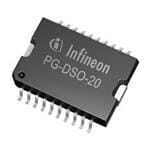
| 描述 | IC REG LDO 5V/TRACKING 20DSO低压差稳压器 Triple Voltage Regulator |
| 产品分类 | |
| 品牌 | Infineon Technologies |
| 产品手册 | http://www.infineon.com/dgdl/TLE4471_DS_16.pdf?folderId=db3a304314dca38901152836c5a412ab&fileId=db3a30431ff9881501201f6b111f4cf1 |
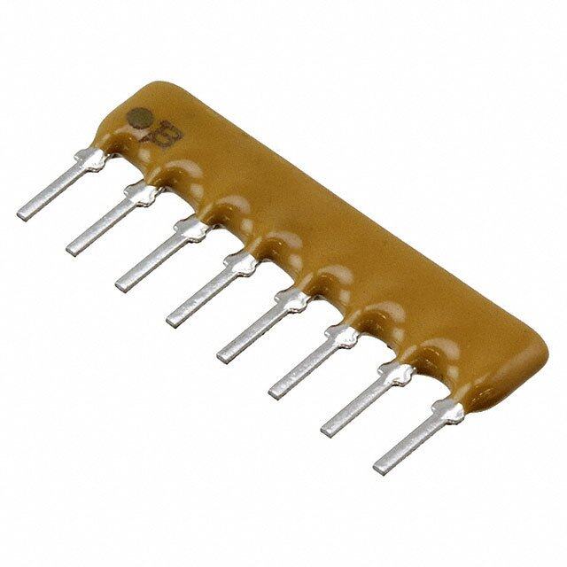
| 产品图片 |
|
| rohs | 符合RoHS无铅 / 符合限制有害物质指令(RoHS)规范要求 |
| 产品系列 | 电源管理 IC,低压差稳压器,Infineon Technologies TLE4471G- |
| 数据手册 | http://www.infineon.com/dgdl/TLE4471_DS_16.pdf?folderId=db3a304314dca38901152836c5a412ab&fileId=db3a30431ff9881501201f6b111f4cf1 |
| 产品型号 | TLE4471G |
| 产品目录页面 | |
| 产品种类 | 低压差稳压器 |
| 供应商器件封装 | PG-DSO-20 |
| 其它名称 | TLE4471GCT |
| 包装 | 剪切带 (CT) |
| 参考电压 | 4.5 V |
| 商标 | Infineon Technologies |
| 回动电压—最大值 | 600 mV at 50 mA |
| 安装类型 | 表面贴装 |
| 安装风格 | SMD/SMT |
| 封装 | Reel |
| 封装/外壳 | 20-SOIC(0.433",11.00mm 宽)裸焊盘 |
| 封装/箱体 | PDSO-20 |
| 工作温度 | -40°C ~ 150°C |
| 工厂包装数量 | 800 |
| 最大工作温度 | + 150 C |
| 最大输入电压 | 40 V |
| 最小工作温度 | - 40 C |
| 最小输入电压 | + 5.5 V |
| 标准包装 | 1 |
| 电压-跌落(典型值) | 0.25V @ 450mA,-,- |
| 电压-输入 | 5.5 V ~ 40 V |
| 电压-输出 | 5V,跟踪 |
| 电压调节准确度 | 2 % |
| 电流-输出 | 450mA, 100mA, 50mA |
| 电流-限制(最小值) | 550mA,110mA,55mA |
| 稳压器拓扑 | 正,固定式和可调式 |
| 稳压器数 | 3 |
| 系列 | TLE4471 |
| 线路调整率 | 25 mV |
| 负载调节 | 25 mV |
| 输入偏压电流—最大 | 1.8 mA |
| 输出电压 | 5 V |
| 输出电流 | 450 mA |
| 输出端数量 | 3 Output |
| 输出类型 | Fixed |
| 零件号别名 | SP000305246 TLE4471GAUMA1 |


- 商务部:美国ITC正式对集成电路等产品启动337调查
- 曝三星4nm工艺存在良率问题 高通将骁龙8 Gen1或转产台积电
- 太阳诱电将投资9.5亿元在常州建新厂生产MLCC 预计2023年完工
- 英特尔发布欧洲新工厂建设计划 深化IDM 2.0 战略
- 台积电先进制程称霸业界 有大客户加持明年业绩稳了
- 达到5530亿美元!SIA预计今年全球半导体销售额将创下新高
- 英特尔拟将自动驾驶子公司Mobileye上市 估值或超500亿美元
- 三星加码芯片和SET,合并消费电子和移动部门,撤换高东真等 CEO
- 三星电子宣布重大人事变动 还合并消费电子和移动部门
- 海关总署:前11个月进口集成电路产品价值2.52万亿元 增长14.8%


PDF Datasheet 数据手册内容提取
Triple Voltage Regulator TLE 4471 Features • Triple Voltage Regulator (cid:127) Output Voltage 5 V with 450 mA Current Capability (cid:127) Two tracked Outputs for 50 mA and 100 mA (cid:127) Enable Function for main and tracked Output(s) (cid:127) Reset with adjustable Threshold (cid:127) Undervoltage- and Power On-Reset (cid:127) Watchdog (cid:127) Independent Watchdog - and Reset delay (cid:127) Wide Temperature Range (cid:127) Overtemperature Protection (cid:127) Overvoltage Protection (cid:127) Reverse Polarity Proof (cid:127) Green Product (RoHS compliant) (cid:127) AEC Qualified Functional Description The TLE 4471 is a monolithic integrated very low-drop triple voltage regulator. The main output supplies loads up to 450 mA and the additional tracked outputs can provide up to 50 mA and 100 mA. In addition the device includes a watchdog for microcontroller- supervision, an undervoltage reset, a power on reset and extended enabling features. The watchdog and reset timing can be chosen independently of each other. The TLE 4471 is available in a Power PG-DSO-20 package. It is designed to supply microprocessor systems under the severe condition of automotive applications and therefore it is equipped with additional protection against overload, short circuit and overtemperature. Of course the TLE 4471 can be used in other applications as well. The TLE 4471 operates in the temperature range of T = -40 to 150 °C. j Type Package TLE 4471 G Power PG-DSO-20 Data Sheet 1 Rev. 1.6, 2009-02-03
TLE 4471 Self Protection - Over Temperature - Short Circuit - Reverse Polarity Proof ESD Protection I Main E1 ≥1 5 V ±2%, 450 mA Regulator E2 Q1 E3 Tracker 1 100 mA, ±0.5% Tracking Q2 Reference Voltage REF2 Tracker 2 50 mA, ±0.5% Tracking EN Q3 Reference Voltage REF3 Reset Generator Reset DR Delay R Reset RADJ Level Adjust W Watchdog DW TLE 4471 AES02864 Figure 1 Block Diagram Data Sheet 2 Rev. 1.6, 2009-02-03
TLE 4471 GND 1 20 GND E1 2 19 DW I 3 18 W Q2 4 17 Q3 REF2 5 16 E3 R 6 15 REF3 DR 7 14 EN E2 8 13 N.C. Q1 9 12 RADJ GND 10 11 GND AEP02865 Figure 2 Pin Configuration (top view) Table 1 Pin Definitions and Functions Pin No. Symbol Function 1, 10, 11, GND GROUND; all four pins connected to the heat sink 20 2 E1 Enable 1; Enable for Main Output Q1 and Q2; E1, E2 and E3 are ored together; connect to GND, if not needed. 3 I Input; block to ground directly at the IC for line compensation. 4 Q2 Tracking Output Q2; block to GND with min. 10 µF with ESR < 3 Ω. 5 REF2 Reference Output; Reference Voltage related to Q2. 6 R Reset Output; the open collector Output is connected to Q1 via an integrated resistor. 7 DR Reset Delay; connect a capacitor to GND for reset delay time adjustment. 8 E2 Enable 2; Enable for Main Output Q1 and Q2; E1, E2 and E3 are ored together; connect to GND, if not needed. 9 Q1 Main Output Q1; block to GND with min. 22 µF, ESR < 3 Ω. 12 RADJ Reset Switching Threshold Adjust; The reset threshold can be set individually with an external voltage divider at the pin. If it is connected straight to GND the reset threshold remains at 4.65 V. 13 NC Not Connected Data Sheet 3 Rev. 1.6, 2009-02-03
TLE 4471 Table 1 Pin Definitions and Functions (cont’d) Pin No. Symbol Function 14 EN Enable Input; enables Q3 15 REF3 Reference Output; Reference Voltage related to Q3. 16 E3 Enable 3; Enable for Main Output Q1 and Q2; E1, E2 and E3 are ored together; connect to GND, if not needed. 17 Q3 Tracker Output Q3; block to GND with min. 10 µF with ESR < 3 Ω. 18 W Watchdog Trigger Input; positive edge triggered input for monitoring a microcontroller. 19 DW Watchdog Delay; connect a capacitor to GND for watchdog trigger time adjustment. Data Sheet 4 Rev. 1.6, 2009-02-03
TLE 4471 Table 2 Absolute Maximum Ratings T = -40 to 150 °C j Parameter Symbol Limit Values Unit Notes Min. Max. Input I Input voltage V -45 42 V – I – 60 V t < 400 ms Main Output Q1 Output voltage V -0.3 7 V – Q1 Output current I – – mA internally limited Q1 Tracking Output Q2 Output voltage V -2 27 V – Q2 Output current I – – mA internally limited Q2 Tracking Output Q3 Output voltage V -2 27 V – Q3 Output current I -5 – mA internally limited Q3 Enable Input E1 Input voltage V -0.3 16 V – E1 Input current I -20 20 mA – E1 Enable Input E2 Input voltage V -0.3 6.5 V – E2 Input current I – – mA internally limited E2 Enable Input E3 Input voltage V -0.3 16 V – E3 Input current I -20 20 mA – E3 Enable Input EN Input voltage V -0.3 7 V – EN Input current I – – mA internally limited EN Reference Output REF2 Output voltage V -0.3 4.5 V – REF2 Output current I – – mA – REF2 Data Sheet 5 Rev. 1.6, 2009-02-03
TLE 4471 Table 2 Absolute Maximum Ratings (cont’d) T = -40 to 150 °C j Parameter Symbol Limit Values Unit Notes Min. Max. Reference Output REF3 Output voltage V -0.3 4.5 V – REF3 Output current I – – mA – REF3 Reset Adjust Input RADJ Input Voltage V -0.3 7 V – RADJ Input Current I – – mA internally limited RADJ Reset Delay DR Voltage V -0.3 7 V – DR Reset Output R Voltage V -0.3 7 V – R Watchdog Delay DW Voltage V -0.3 7 V – DW Watchdog Input W Input voltage V -0.3 7 V – W Input current I – – mA – W Temperature Junction temperature T -50 150 °C – j Storage temperature T -65 150 °C – Stg Thermal Data Junction-ambient R – – K/W – thja R – 4 K/W – thjp ESD Human Body Model – -2 2 kV – Note: Stresses above those listed here may cause permanent damage to the device. Exposure to absolute maximum rating conditions for extended periods may affect device reliability. Data Sheet 6 Rev. 1.6, 2009-02-03
TLE 4471 Table 3 Operating Range Parameter Symbol Limit Values Unit Notes Min. Max. Input voltage V 5.5 40 V – I Junction temperature T -40 150 °C – j Shutdown voltage V – 44 V – shut threshold Note: In the operating range, the functions given in the circuit description are fulfilled. Data Sheet 7 Rev. 1.6, 2009-02-03
TLE 4471 Table 4 Characteristics V = 13.5 V; T = -40 °C < T < 125 °C I j j Parameter Symbol Limit Values Unit Measuring Condition Min. Typ. Max. Main Output Q1 Output voltage V 4.9 5.0 5.1 V 10 mA < I < 450 mA; Q1 Q1 5.5 V < V < 19 V I Output voltage V 4.8 5.0 5.2 V 10 mA < I < 300 mA; Q1 Q1 5.5 V < V < 28 V I Output voltage V 4.8 5.0 5.2 V 10 mA < I < 200 mA; Q1 Q1 5.5 V < V < 40 V I Output current limit I 550 – 1500 mA V = 0.1 V Q1 Q1 Output voltage drop V – 0.25 0.55 V I = 450 mA1) DR Q1 Line regulation ∆V -25 – 25 mV 8 V ≤ V ≤ 16 V; Q1 I I = 10 mA Q1 Load regulation ∆V -25 – 25 mV 10 mA < I < 450 mA; Q1 Q1 V = 7 V I Power Supply Ripple PSRR – 30 – dB C = 22 µF; Q1 Rejection 20 Hz < f < 20 kHz; r V = 0.5 V2) PP Output capacitor C 22 – – µF 2) Q1 ESR of output ESR – – 3 Ω at 10 kHz2) capacitor Tracked Output Q2 Output voltage ∆V = -25 – 25 mV 5.7 V < V < 19 V; Q2 I tracking accuracy V - V 1 mA < I < 100 mA Q2 Q1 Q2 Output voltage ∆V = -25 – 25 mV 5.7 V < V < 28 V; Q2 I tracking accuracy V - V 1 mA < I < 80 mA Q2 Q1 Q2 Output voltage ∆V = -25 – 25 mV 5.7 V < V < 40 V; Q2 I tracking accuracy V - V 1 mA < I < 50 mA Q2 Q1 Q2 Output current limit I 110 – – mA V = 0.1 V Q2 Q2 Output voltage drop V – – 0.6 V I = 100 mA DR2 Q2 Power Supply Ripple PSRR – 30 – dB 20 Hz < f < 20 kHz; r Rejection V = 0.5 V; PP C = 10 µF2) Q2 Data Sheet 8 Rev. 1.6, 2009-02-03
TLE 4471 Table 4 Characteristics (cont’d) V = 13.5 V; T = -40 °C < T < 125 °C I j j Parameter Symbol Limit Values Unit Measuring Condition Min. Typ. Max. Output capacitor C 10 – – µF 2) Q2 ESR of output ESR – – 3 Ω at 10 kHz2) capacitor Tracked Output Q3 Output voltage ∆V = -25 – 25 mV 5.7 V < V < 19 V; Q3 I tracking accuracy V - V 1 mA < I < 50 mA Q3 Q1 Q3 Output voltage ∆V = -25 – 25 mV 5.7 V < V < 28 V; Q3 I tracking accuracy V - V 1 mA < I < 40 mA Q3 Q1 Q3 Output voltage ∆V = -25 – 25 mV 5.7 V < V < 40 V; Q3 I tracking accuracy V - V 1 mA < I < 25 mA Q3 Q1 Q3 Output current limit I 55 – 150 mA V = 0.1 V Q3 Q3 Output voltage drop V – – 0.6 V 1 mA ≤ I ≤ 50 mA DR3 Q3 Power Supply Ripple PSRR – 30 – dB 20 Hz < f < 20 kHz; r Rejection V = 0.5 V; PP C = 10 µF2) Q3 Output capacitor C 10 – – µF 2) Q3 ESR of output ESR – – 3 Ω at 10 kHz2) capacitor Matching error ∆V = -25 – 25 mV – Q2,3 between V and V V - V Q2 Q3 Q3 Q2 Current Consumption Quiescent current I – – 20 µA Q1 OFF, Q2 OFF; Q3 q (standby) OFF Current consumption; I – 1100 – µA Q3 OFF, I < 1 mA; q Q1 I = I - I I < 1 mA q I Q Q2 Current consumption; I – 1800 – µA I < 10 mA; q Q1 I = I - I I < 1 mA; q I Q Q2 I < 1 mA Q3 Data Sheet 9 Rev. 1.6, 2009-02-03
TLE 4471 Table 4 Characteristics (cont’d) V = 13.5 V; T = -40 °C < T < 125 °C I j j Parameter Symbol Limit Values Unit Measuring Condition Min. Typ. Max. Enable Function E1, E2, E3, EN E1 On threshold V 3.5 4.1 4.5 V V > 4.8 V; V > 4.8 V E1, on Q1 Q2 E1 Off threshold V 1.5 – 2.5 V – E1, off E1 High input current I – 50 – µA V = 16 V E1, on E1 E1 Low input current I -1 – 5 µA V = 0 V E1, off E1 E2 On threshold V 1.3 1.7 2.0 V V > 4.8 V; V > 4.8 V E2, on Q1 Q2 E2 Off threshold V 0.8 1.2 1.7 V – E2, off E2 resistance to GND R 5 15 40 kΩ – E2 E3 On threshold V 3.5 – 4.5 V V > 4.8 V; V > 4.8 V E3, on Q1 Q2 E3 Off threshold V 1.5 – 2.5 V – E3, off E3 High input current I – 50 – µA V = 16 V E3, on E3 E3 Low input current I -1 – 5 µA V = 0 V E3, off E3 EN On threshold V 1.0 1.7 2.3 V V > 4.8 V; Q1 ON EN, on Q3 EN Off threshold V 0.8 1.2 1.7 V V < 0.1 V EN, off Q3 Enable resistance to R 5 15 40 kΩ – EN GND Reset Generator Switching threshold V 4.5 4.65 4.8 V RADJ connected to Q, rth GND Reset headroom V 250 350 500 mV 10 mA < I < 450 mA head Q1 Reset pull-up R 2.4 – 6 kΩ – R Reset output low V – – 0.4 V 1 V < V < V R, low Q1 Q, rth voltage Reset output Low V – – 0.4 V V = 1 V, I = 50 µA R, low Q1 R voltage Reset output High V 4.5 – – V – R, high voltage Reset adjust V 1.25 1.35 1.45 V V > 3.5 V RADJ Q1 threshold Data Sheet 10 Rev. 1.6, 2009-02-03
TLE 4471 Table 4 Characteristics (cont’d) V = 13.5 V; T = -40 °C < T < 125 °C I j j Parameter Symbol Limit Values Unit Measuring Condition Min. Typ. Max. Reset delay charging I 2 4 6 µA V = 1 V DR, ch DR current Reset delay I 60 120 160 mA V = 1 V DR, dis DR discharge current Upper reset timing V 0.9 1.8 2.7 V – DR, dt threshold Lower timing V 0.25 0.4 0.65 V – DR, st threshold Reset delay time t 35 50 70 ms C = 100 nF dr R Reset reaction time t 0.5 – 3 µs C = 100 nF rr R Watchdog Watchdog input R 5 15 40 kΩ – W pull-down resistor Watchdog delay I 2 4 6 µA V = 1 V; V = 2.7 V DW, ch DW DR charging current Watchdog upper V 1.5 1.9 2.5 V – DW, dt timing threshold Watchdog lower V 0 30 200 mV – DW, st timing threshold Watchdog trigger t 35 50 70 ms C = 100 nF wp DW pulse interval Reference Output REF2 Voltage divider ratio V 49.5 50 50.5 % of – REF2 V Q2 Output impedance R 10 – 20 kΩ – REF2 Output clamp voltage – – – 4.5 V – Data Sheet 11 Rev. 1.6, 2009-02-03
TLE 4471 Table 4 Characteristics (cont’d) V = 13.5 V; T = -40 °C < T < 125 °C I j j Parameter Symbol Limit Values Unit Measuring Condition Min. Typ. Max. Reference Output REF3 Voltage divider ratio V 49.5 50 50.5 % of – REF3 V Q3 Output impedance R 10 – 20 kΩ – REF3 Output clamp voltage – – – 4.5 V – 1) Measured when the output voltage V dropped 100 mV from the nominal value. Q 2) Not subject to production test, specified by design. Note: The listed characteristics are ensured over the operating range of the integrated circuit. Typical characteristics specify mean values expected over the production spread. If not otherwise specified, typical characteristics apply at T = 25 °C and A the given supply voltage. Data Sheet 12 Rev. 1.6, 2009-02-03
TLE 4471 I I I Q1 V I Q1 V I Q1 I 22 µF E1 V E1 I E1 Q2 IE2 Q2 VQ2 V E2 10 µF E2 I E3 TLE 4471 I REF2 V E3 E3 REF2 V REF2 I EN V EN EN I I Q3 DR, dis Q3 V DR Q3 C 10 µF IRADJ 100 nDFR IDR, ch I V RADJ REF3 RADJ I REF3 VREF3 W V W W I R DW R V C R DW I GND 100 nF DW, ch I GND AES02866 Figure 3 Measurement Circuit Data Sheet 13 Rev. 1.6, 2009-02-03
TLE 4471 Application Information Q2 Sensor / Peripheral I Tracking V KL.30 BAT Output 2 REF2 optional Main Q1 AD DR RADJ Watchdog / Reset R DW W Controller E1 Ignition KL.15 Enable E2 E3 Logic Enable-Signal EN AD REF3 Tracking Output 3 Q3 Sensor / Peripheral AES02867 Figure 4 Application Diagram Input With an input voltage between 5.5 V < V < 40 V the regulator works in its normal I operating range. If the input voltage exceeds the 40 V up to 60 V for less than 400 ms, e.g. caused by a load dump, the active components are switched off. For compensating line influences and to avoid steep input edges above 1 V/µs an input capacitor is needed. Using a resistor of approx. 1 Ω in series to the input capacitor, the oscillating circuit consisting of input inductance and input capacitor is damped. Data Sheet 14 Rev. 1.6, 2009-02-03
TLE 4471 Output Voltage To obtain an output voltage of V = 5 V with an accuracy of 2% at the main output Q1 Q1 an input voltage in the range of 5.5 V < V < 40 V is needed. The main output Q1 supplies I 5 V with 450 mA current capability. For stability it requires an output capacitor of at least 22 µF and a maximum ESR of 3 Ω. The two outputs Q2 and Q3 are tracked to Q1 and can supply currents of 100 mA and 50 mA. So any undervoltage condition or shutdown of Q1 will cause the same effect to Q2 and Q3. For Stability both outputs require an output capacitor of at least 10 µF with ESR < 3 Ω each. Q2 is switched on and off simultaneously with Q1, while the tracked output Q3 can be enabled or disabled individually. Two reference outputs REF2, REF3 with voltages of V = V /2 and V = V /2 are REF2 Q2 REF3 Q3 also available. In case of an overvoltage at the tracker outputs, the voltage references are limited internally to 4.5 V. Output Current The output current is a function of the input voltage. For high input voltages above 22 V, the output current is reduced linear. This is designed into the regulator for protection. Above 42 V the regulator is switched off. The thermal shutdown switches the regulator off, if it exceeds the thermal threshold of 160 °C typical. It is switched on again, as soon as the regulator is cooled down by typical 10 K (thermal hysteresis). Please note the device should not be operated above a junction temperature of 150 °C for long term reliability. Enable Function The TLE 4471 includes the possibility of enabling the main and tracked outputs. Three ORed enable inputs E1, E2, E3 are used to control the main output Q1 and the tracked output Q2. E1 and E3 can be supplied from the battery line or ignition key with input voltages up to 16 V. The enable inputs should be protected by a series resistor and a capacitor, e.g. R = R = 22 kΩ, C = C = 2.2 nF. E2 is intended for connection to E1 E3 E1 E3 the microcontroller. A logic HIGH at any enable input will switch on the related regulator and/or tracker. A separate enabling pin EN is available to switch on and off the second tracked output Q3 separately by the microcontroller. Reset The power on reset feature is necessary for a defined start of the microprocessor during power up. When the output voltage of the main regulator has reached the reset threshold voltage the reset delay capacitor C is charged. After a certain time, the reset delay time DR t , the voltage at the capacitor equals the upper reset timing threshold and the reset dr output goes HIGH. Data Sheet 15 Rev. 1.6, 2009-02-03
TLE 4471 The reset delay time t is defined by the reset delay capacitor C at pin DR and can be dr DR calculated as follows: V t = C × -----D---R---,-d---t (1) rd DR I DR,ch Definitions: (cid:127) C = reset delay capacitor DR (cid:127) t = reset delay time required by the application dr (cid:127) V = typical 1.8 V for power up reset DR, dt (cid:127) I = charge current typical 4 µA DR, ch For a delay capacitor C = 100 nF the typical power up reset delay time is 45 ms. DR The undervoltage reset circuitry supervises the output voltage. In case V falls below Q1 the reset threshold the reset output is set LOW after the reset reaction time t (discharge rr of the reset delay capacitor). The reset LOW signal is held down to an output voltage V Q1 of 1 V. Both, the reset reaction time and the reset delay time are defined by the capacitor value. The reset reaction time t is the time it takes the voltage regulator to set its reset output rr LOW after the output voltage has dropped below the reset threshold. The reset reaction time can be calculated using the following equation: V – V t = C × -----D---R---,-d---t-----------D---R----,-s--t (2) rr DR I DR,dis Data Sheet 16 Rev. 1.6, 2009-02-03
TLE 4471 V Ι t V <t Q rr V Q, rth t V D V DR, dt V DR, st t t t rr dr V RO t Power-on-Reset Thermal Voltage Dip Undervoltage Secondary Overload Shutdown at Input Spike at Output AED03045 Figure 5 Reset Timing The reset output is an open collector output with a pull-up-resistor of typical 4 kΩ to Q1. An external pull-up can be added with a resistor value of at least 20 kΩ. In addition the reset switching threshold can be adjusted by an external voltage divider. The feature is useful with microprocessors which guarantee safe operation down to voltages below the internally set reset threshold of 4.65 typical. Data Sheet 17 Rev. 1.6, 2009-02-03
TLE 4471 TLE 4471 I Q Bandgap Reference R RTH1 1.36 V R V rth,ref 1 RADJ R RTH2 AES02877 Figure 6 Adjusting the Reset Threshold For using the preadjusted reset threshold voltage of typical V = 4.65 V, the pin RADJ Q, rth has to be connected to GND. If a lower reset threshold is required by the system, a voltage divider defines the reset threshold V between 3.5 V and 4.65 V: Q, rthext R V = V × 1 + -----R---T---H---1- (3) Q,rthext rth,ref R RTH2 V is typical 1.35 V. rth,ref Data Sheet 18 Rev. 1.6, 2009-02-03
TLE 4471 Watchdog The reset and watchdog timing can be defined independently of each other by two delay capacitors C and C at pins DR and DW. DR DW The watchdog function supervises the microcontroller including time base failures. If there is no positive edge within a certain pulse repetition time t or the trigger pulse is wp too short a reset is generated. Programming of the max. repetition time is done by a delay capacitor C at pin DW. DW The frequency of the watchdog pulses generated by the microcontroller has to be higher than the minimum pulse sequence t set by the external reset delay capacitor C . The wp DW pulse repetition time can be calculated as follows: V – V t = C × -----D---W----,-d---t-----------D---W----,--s--t (4) wp DW I DW,ch V I t V Q1 t t>10 µs t>25 µs V W t t WP V V DW DW,dt V DW,st t V DR V DR,dt V DR,st t t t dr rr V R t Missing edge Watchdog pulses at Watchdog too short AET03000 Figure 7 Watchdog Timing If the watchdog is not used in an application the pin WD has to be connected to GND. Data Sheet 19 Rev. 1.6, 2009-02-03
TLE 4471 Power Supply Ripple Rejection PSRR of Power Supply Ripple Rejection PSRR of Main Output Q1 versus Frequency f Output Q2 versus Frequency f AED02996 AED02995 80 80 dB C = 22 µF dB CQ2 = 10 µF Q1 PSRR PSRR I = 10 mA Q1 70 70 I = 450 mA Q1 I = 1 mA Q2 60 60 50 50 I = 100 mA Q2 40 40 30 30 100 101 102 103 104Hz105 100 101 102 103 Hz 105 f f Power Supply Ripple Rejection PSRR of Output Q3 versus Frequency f AED02997 80 dB C = 10 µF Q3 PSRR 70 I = 1 mA Q3 60 50 40 I = 50 mA Q3 30 100 101 102 103 Hz 105 f Data Sheet 20 Rev. 1.6, 2009-02-03
TLE 4471 Enable Currents I , I and Output Enable Currents I , I and Output E1 E3 E2 EN Voltage V versus Enable Voltages Voltage V versus Enable Voltages Q1 Q3 V , V V , V E1 E3 E2 EN AED02998 AED02999 5 7.5 250 7.5 µA V µA V I , I V I , I V E1 E3 Q1 E2 EN Q3 4 6 200 6 3 4.5 150 4.5 2 3 100 3 1 1.5 50 1.5 0 0 0 0 0 1 2 3 4 V 5 0 0.5 1 1.5 2 V 2.5 V , V V , V E1 E3 E2 EN Data Sheet 21 Rev. 1.6, 2009-02-03
TLE 4471 Package Outlines 1 X. 11±0.151) B 1.1±0.1 +0.10 3.25±0. 3.5 MA 2.8 2+50.07-0.02 3˚ 0. 5˚± 15.74±0.1 1.3 6.3 (Heatslug) Heatslug 1.27 0.1 (Mold) 0.95±0.15 0.4+0.13 0.25M A 20x 14.2±0.3 0.25 B Bottom View 20 11 11 20 0.1 al) 0.1 al) 3.2± (Met 5.9± (Met Index Marking Heatslug 1 10 10 1 1 x 45˚ 13.7 -0.2 15.9±0.151) (Metal) A (Mold) 1)Does not include plastic or metal protrusion of 0.15 max. per side GPS05791 Figure 8 Power PG-DSO-20 (Plastic Dual Small Outline) Green Product (RoHS compliant) To meet the world-wide customer requirements for environmentally friendly products and to be compliant with government regulations the device is available as a green product. Green products are RoHS-Compliant (i.e Pb-free finish on leads and suitable for Pb-free soldering according to IPC/JEDEC J-STD-020). Find all of our packages, sorts of packing and others in our Infineon Internet Page “Packages”: http://www.infineon.com/packages. SMD = Surface Mounted Device Dimensions in mm Data Sheet 22 Rev. 1.6, 2009-02-03
TLE 4471 Revision History Version Date Changes Rev. 1.6 2009-02-03 Package bond wire modification according to PCN No. 2007-090. Change of package name in datasheet to “Power PG-DSO-20”. No change of package outline. Rev. 1.5 2007-03-20 Initial version of RoHS-compliant derivate of TLE 4471 Page 1: AEC certified statement added Page 1 and Page 22: RoHS compliance statement and Green product feature added Page 1 and Page 22: Package changed to RoHS compliant version Legal Disclaimer updated Rev. 1.4 2005-01-28 Parameter “Output Clamp Voltage” REF2 and REF3: Max. value changed from 4V to 4.5V in order to align with the Maximum Ratings Data Sheet 23 Rev. 1.6, 2009-02-03
Edition 2009-02-03 Published by Infineon Technologies AG 81726 Munich, Germany © 2009 Infineon Technologies AG All Rights Reserved. Legal Disclaimer The information given in this document shall in no event be regarded as a guarantee of conditions or characteristics. With respect to any examples or hints given herein, any typical values stated herein and/or any information regarding the application of the device, Infineon Technologies hereby disclaims any and all warranties and liabilities of any kind, including without limitation, warranties of non-infringement of intellectual property rights of any third party. Information For further information on technology, delivery terms and conditions and prices, please contact the nearest Infineon Technologies Office (www.infineon.com). Warnings Due to technical requirements, components may contain dangerous substances. For information on the types in question, please contact the nearest Infineon Technologies Office. Infineon Technologies components may be used in life-support devices or systems only with the express written approval of Infineon Technologies, if a failure of such components can reasonably be expected to cause the failure of that life-support device or system or to affect the safety or effectiveness of that device or system. Life support devices or systems are intended to be implanted in the human body or to support and/or maintain and sustain and/or protect human life. If they fail, it is reasonable to assume that the health of the user or other persons may be endangered.
Mouser Electronics Authorized Distributor Click to View Pricing, Inventory, Delivery & Lifecycle Information: I nfineon: TLE4471G TLE4471GXT