ICGOO在线商城 > TLE42994GM

 Datasheet下载
- 型号: TLE42994GM
- 制造商: Infineon
- 库位|库存: xxxx|xxxx
- 要求:
| 数量阶梯 | 香港交货 | 国内含税 |
| +xxxx | $xxxx | ¥xxxx |
查看当月历史价格
查看今年历史价格
TLE42994GM产品简介:
ICGOO电子元器件商城为您提供TLE42994GM由Infineon设计生产,在icgoo商城现货销售,并且可以通过原厂、代理商等渠道进行代购。 提供TLE42994GM价格参考¥6.51-¥6.51以及InfineonTLE42994GM封装/规格参数等产品信息。 你可以下载TLE42994GM参考资料、Datasheet数据手册功能说明书, 资料中有TLE42994GM详细功能的应用电路图电压和使用方法及教程。
| 参数 | 数值 |
| 产品目录 | 集成电路 (IC) |
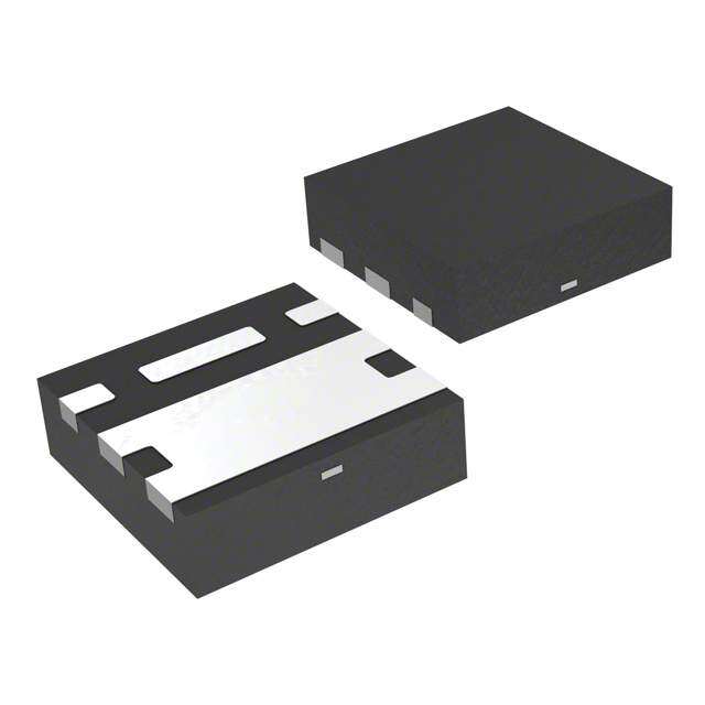
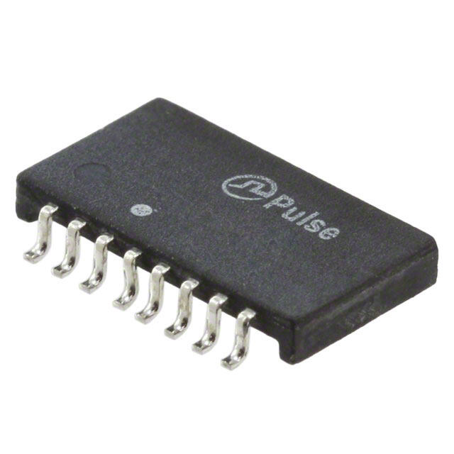
| 描述 | IC REG LDO 5V 0.15A 14DSO |
| 产品分类 | |
| 品牌 | Infineon Technologies |
| 数据手册 | http://www.infineon.com/dgdl/TLE42994-Data-Sheet-12-Infineon.pdf?folderId=db3a304314dca3890115039cf70d0bf0&fileId=db3a30431f848401011fb758a96b590d&ack=t |
| 产品图片 |
|
| 产品型号 | TLE42994GM |
| PCN封装 | |
| PCN设计/规格 | |
| rohs | 无铅 / 符合限制有害物质指令(RoHS)规范要求 |
| 产品系列 | - |
| 供应商器件封装 | PG-DSO-14 |
| 其它名称 | TLE42994GMCT |
| 包装 | 剪切带 (CT) |
| 安装类型 | 表面贴装 |
| 封装/外壳 | 14-SOIC(0.154",3.90mm 宽) |
| 工作温度 | -40°C ~ 150°C |
| 标准包装 | 1 |
| 电压-跌落(典型值) | 0.22V @ 100mA |
| 电压-输入 | 5.5 V ~ 45 V |
| 电压-输出 | 5V |
| 电流-输出 | 150mA |
| 电流-限制(最小值) | 150mA |
| 稳压器拓扑 | 正,固定式 |
| 稳压器数 | 1 |


- 商务部:美国ITC正式对集成电路等产品启动337调查
- 曝三星4nm工艺存在良率问题 高通将骁龙8 Gen1或转产台积电
- 太阳诱电将投资9.5亿元在常州建新厂生产MLCC 预计2023年完工
- 英特尔发布欧洲新工厂建设计划 深化IDM 2.0 战略
- 台积电先进制程称霸业界 有大客户加持明年业绩稳了
- 达到5530亿美元!SIA预计今年全球半导体销售额将创下新高
- 英特尔拟将自动驾驶子公司Mobileye上市 估值或超500亿美元
- 三星加码芯片和SET,合并消费电子和移动部门,撤换高东真等 CEO
- 三星电子宣布重大人事变动 还合并消费电子和移动部门
- 海关总署:前11个月进口集成电路产品价值2.52万亿元 增长14.8%
PDF Datasheet 数据手册内容提取
TLE42994 Low Dropout Fixed Voltage Regulator TLE42994G TLE42994GM TLE42994E Data Sheet Rev. 1.2, 2014-07-03 Automotive Power
Low Dropout Fixed Voltage Regulator TLE42994 1 Overview Features • Output Voltage 5 V ± 2% • Ouput Current up to 150mA • Extreme Low Current Consumption In ON State • Enable Function: Below 1µA Current Consumption In OFF State • Early Warning PG-DSO-8 • Power-on and Undervoltage Reset with Programmable Delay Time • Reset Low Down to V = 1V Q • Adjustable Reset Threshold • Very Low Dropout Voltage • Output Current Limitation • Reverse Polarity Protection • Overtemperature Protection • Suitable for Use in Automotive Electronics • Wide Temperature Range from -40 °C up to 150 °C • Input Voltage Range from -42 V to 45 V PG-DSO-14 • Green Product (RoHS compliant) • AEC Qualified Description The TLE42994 is a monolithic integrated low dropout voltage regulator, especially designed for automotive applications that need to be in ON state during the car’s engine is turned off. An input voltage up to 45V is regulated to an output voltage of 5.0V. The component is able to drive loads up to 150mA. It is short-circuit protected by the implemented current limitation and has an integrated overtemperature shutdown. A reset signal is generated for an output voltage V of Q,rt PG-SSOP-14 exposed pad typically 4.65V. This threshold can be decreased by an external Type Package Marking TLE42994G PG-DSO-8 42994G TLE42994GM PG-DSO-14 42994GM TLE42994E PG-SSOP-14 exposed pad 42994E Data Sheet 2 Rev. 1.2, 2014-07-03
TLE42994 Overview resistor divider. The power-on reset delay time can be programmed by the external delay capacitor. The additional sense comparator provides an early warning function: Any voltage (e.g. the input voltage) can be monitored, an under-voltage condition is indicated by setting the comparator’s output to low. The TLE42994GM (PG-DSO-14 package) and TLE42994E (PG-SSOP-14 exposed pad package) include additionally an Enable function permitting enabling/disabling the regulator. In case the regulator is disabled it consumes less current than 1µA. Dimensioning Information on External Components The input capacitor C is recommended for compensation of line influences. The output capacitor C is necessary I Q for the stability of the control loop. Circuit Description The control amplifier compares a reference voltage to a voltage that is proportional to the output voltage and drives the base of the series transistor via a buffer. Saturation control as a function of the load current prevents any oversaturation of the power element. The component also has a number of internal circuits for protection against: • Overload • Overtemperature • Reverse polarity Data Sheet 3 Rev. 1.2, 2014-07-03
TLE42994 Block Diagram 2 Block Diagram I Q Band- Current R Gap- and SO Reference Saturation Control R RO SO SI Reference RO Reset Control RADJ D GND AEB03103 Figure1 Block Diagram TLE42994G (package PG-DSO-8) Data Sheet 4 Rev. 1.2, 2014-07-03
TLE42994 Block Diagram TLE 4299 I Q Band- Current R Gap- and SO Reference Saturation Control Inhibit R IENNH Enable RO Control SO SI Reference RO Reset Control RADJ D GND AEB03104 Figure2 Block Diagram TLE42994GM, TLE42994E (packages PG-DSO-14, PG-SSOP-14 exposed pad) Data Sheet 5 Rev. 1.2, 2014-07-03
TLE42994 Pin Configuration 3 Pin Configuration 3.1 Pin Assignment TLE42994G (PG-DSO-8) Ι 1 8 Q SΙ 2 7 SO RADJ 3 6 RO D 4 5 GND AEP01668 Figure3 Pin Configuration (top view) 3.2 Pin Definitions and Functions TLE42994G (PG-DSO-8) Pin Symbol Function 1 I Input for compensating line influences, a capacitor to GND close to the IC terminals is recommended 2 SI Sense Input connect the voltage to be monitored; connect to Q if the sense comparator is not needed 3 RADJ Reset Threshold Adjust connect an external voltage divider to adjust reset threshold; connect to GND for using internal threshold 4 D Reset Delay Timing connect a ceramic capacitor to GND for adjusting the reset delay time; leave open if the reset function is not needed 5 GND Ground 6 RO Reset Output open collector output; internally linked to the output via a 20kΩ pull-up resistor; leave open if the reset function is not needed 7 SO Sense Output open collector output; internally linked to the output via a 20kΩ pull-up resistor; leave open if the sense comparator is not needed 8 Q Output block to GND with a capacitor close to the IC terminals, respecting the values given for its capacitance C and ESR in “Functional Range” on Page12 Q Data Sheet 6 Rev. 1.2, 2014-07-03
TLE42994 Pin Configuration 3.3 Pin Assignment TLE42994GM (PG-DSO-14) RADJ 1 14 SI D 2 13 I GND 3 12 GND GND 4 11 GND GND 5 10 GND EN 6 9 Q RO 7 8 SO PinConfig_PG-DSO-14.vsd Figure4 Pin Configuration (top view) 3.4 Pin Definitions and Functions TLE42994GM (PG-DSO-14) Pin Symbol Function 1 RADJ Reset Threshold Adjust connect an external voltage divider to adjust reset threshold; connect to GND for using internal threshold 2 D Reset Delay Timing connect a ceramic capacitor to GND for adjusting the reset delay time; leave open if the reset function is not needed 3, 4, 5 GND Ground connect all pins to PCB and heatsink area 6 EN Enable high signal enables the regulator; low signal disables the regulator; connect to I if the Enable function is not needed 7 RO Reset Output open collector output; internally linked to the output via a 20kΩ pull-up resistor; leave open if the reset function is not needed 8 SO Sense Output open collector output; internally linked to the output via a 20kΩ pull-up resistor; leave open if the sense comparator is not needed 9 Q Output block to GND with a capacitor close to the IC terminals, respecting the values given for its capacitance C and ESR in the table “Functional Range” on Page12 Q 10, 11, 12 GND Ground connect all pins to PCB and heatsink area Data Sheet 7 Rev. 1.2, 2014-07-03
TLE42994 Pin Configuration Pin Symbol Function 13 I Input for compensating line influences, a capacitor to GND close to the IC terminals is recommended 14 SI Sense Input connect the voltage to be monitored; connect to Q if the sense comparator is not needed Data Sheet 8 Rev. 1.2, 2014-07-03
TLE42994 Pin Configuration 3.5 Pin Assignment TLE42994E (PG-SSOP-14 exposed pad) RADJ 1 14 SI n.c. 2 13 I D 3 12 n.c. GND 4 11 Q EN 5 10 n.c. n.c. 6 9 n.c. RO 7 8 SO PINCONFIG_SSOP-14.VSD Figure5 Pin Configuration (top view) 3.6 Pin Definitions and Functions TLE42994E (PG-SSOP-14 exposed pad) Pin Symbol Function 1 RADJ Reset Threshold Adjust connect an external voltage divider to adjust reset threshold; connect to GND for using internal threshold 2, 6 n.c. not connected leave open or connect to GND 3 D Reset Delay Timing connect a ceramic capacitor to GND for adjusting the reset delay time; leave open if the reset function is not needed 4 GND Ground connect all pins to PCB and heatsink area 5 EN Enable high signal enables the regulator; low signal disables the regulator; connect to I if the Enable function is not needed 7 RO Reset Output open collector output; internally linked to the output via a 20kΩ pull-up resistor; leave open if the reset function is not needed 8 SO Sense Output open collector output; internally linked to the output via a 20kΩ pull-up resistor; leave open if the sense comparator is not needed 9, 10, 12 n.c. not connected leave open or connect to GND 11 Q Output block to GND with a capacitor close to the IC terminals, respecting the values given for its capacitance C and ESR in the table “Functional Range” on Page12 Q 13 I Input for compensating line influences, a capacitor to GND close to the IC terminals is recommended Data Sheet 9 Rev. 1.2, 2014-07-03
TLE42994 Pin Configuration Pin Symbol Function 14 SI Sense Input connect the voltage to be monitored; connect to Q if the sense comparator is not needed PAD – Exposed Pad attach the exposed pad on package bottom to the heatsink area on circuit board; connect to GND Data Sheet 10 Rev. 1.2, 2014-07-03
TLE42994 General Product Characteristics 4 General Product Characteristics 4.1 Absolute Maximum Ratings Table1 Absolute Maximum Ratings1) -40 °C ≤ T ≤ 150°C; all voltages with respect to ground, positive current flowing into pin (unless otherwise j specified) Parameter Symbol Values Unit Note / TestCondition Number Min. Typ. Max. Input I, Enable Input EN, Sense Input SI Voltage V, V , V -40 – 45 V – P_4.1.1 I EN SI Output Q, Reset Output RO, Sense Output SO Voltage V , V , V -0.3 – 7 V – P_4.1.2 Q RO SO Reset Delay D, Reset Threshold RADJ Voltage V , V -0.3 – 7 V – P_4.1.3 D RADJ Temperature Junction Temperature T -40 – 150 °C – P_4.1.4 j Storage Temperature T -50 – 150 °C – P_4.1.5 stg ESD Absorption ESD Absorption V -2 – 2 kV Human Body Model P_4.1.6 ESD,HBM (HBM)2) ESD Absorption V -500 – 500 V Charge Device Model P_4.1.7 ESD,CDM (CDM)3) ESD Absorption V -750 – 750 V Charge Device Model P_4.1.8 ESD,CDM (CDM)3) at corner pins 1) not subject to production test, specified by design 2) ESD susceptibility Human Body Model “HBM” according to AEC-Q100-002 - JESD22-A114 3) ESD susceptibility Charged Device Model “CDM” according to ESDA STM5.3.1 Notes 1. Stresses above the ones listed here may cause permanent damage to the device. Exposure to absolute maximum rating conditions for extended periods may affect device reliability. 2. Integrated protection functions are designed to prevent IC destruction under fault conditions described in the data sheet. Fault conditions are considered as “outside” normal operating range. Protection functions are not designed for continuous repetitive operation. Data Sheet 11 Rev. 1.2, 2014-07-03
TLE42994 General Product Characteristics 4.2 Functional Range Table2 Functional Range Parameter Symbol Values Unit Note / TestCondition Number Min. Typ. Max. Input Voltage V 5.5 – 45 V – P_4.2.1 I Output Capacitor’s Requirements C 22 – – µF –1) P_4.2.2 Q for Stability Output Capacitor’s Requirements ESR(C ) – – 3 Ω –2) P_4.2.3 Q for Stability Junction Temperature T -40 – 150 °C – P_4.2.4 j 1) the minimum output capacitance requirement is applicable for a worst case capacitance tolerance of 30% 2) relevant ESR value at f=10kHz Note:Within the functional range the IC operates as described in the circuit description. The electrical characteristics are specified within the conditions given in the related electrical characteristics table. Data Sheet 12 Rev. 1.2, 2014-07-03
TLE42994 General Product Characteristics 4.3 Thermal Resistance Table3 Thermal Resistance Parameter Symbol Values Unit Note / TestCondition Number Min. Typ. Max. TLE42994G (PG-DSO-8) Junction to Soldering Point1) R – – 60 K/W measured to pin 5 P_4.3.1 thJSP Junction to Ambient1) R – 113 – K/W FR4 2s2p board2) P_4.3.2 thJA Junction to Ambient1) R – 185 – K/W FR4 1s0p board, footprint P_4.3.3 thJA only3) Junction to Ambient1) R – 142 – K/W FR4 1s0p board, 300mm2 P_4.3.4 thJA heatsink area on PCB3) Junction to Ambient1) R – 136 – K/W FR4 1s0p board, 600mm2 P_4.3.5 thJA heatsink area on PCB3) TLE42994GM (PG-DSO-14) Junction to Soldering Point1) R – – 30 K/W measured to all GND pins P_4.3.6 thJSP Junction to Ambient1) R – 63 – K/W FR4 2s2p board2) P_4.3.7 thJA Junction to Ambient1) R – 112 – K/W FR4 1s0p board, footprint P_4.3.8 thJA only3) Junction to Ambient1) R – 73 – K/W FR4 1s0p board, 300mm2 P_4.3.9 thJA heatsink area on PCB3) Junction to Ambient1) R – 65 – K/W FR4 1s0p board, 600mm2 P_4.3.10 thJA heatsink area on PCB3) TLE42994E (PG-SSOP-14 exposed pad) Junction to Case1) R – 10 – K/W – P_4.3.11 thJC Junction to Ambient1) R – 47 – K/W FR4 2s2p board2) P_4.3.12 thJA Junction to Ambient1) R – 140 – K/W FR4 1s0p board, footprint P_4.3.13 thJA only3) Junction to Ambient1) R – 63 – K/W FR4 1s0p board, 300mm2 P_4.3.14 thJA heatsink area on PCB3) Junction to Ambient1) R – 53 – K/W FR4 1s0p board, 600mm2 P_4.3.15 thJA heatsink area on PCB3) 1) not subject to production test, specified by design 2) Specified R value is according to Jedec JESD51-2,-5,-7 at natural convection on FR4 2s2p board; The Product thJA (Chip+Package) was simulated on a 76.2 x 114.3 x 1.5 mm³ board with 2 inner copper layers (2 x 70µm Cu, 2 x 35µm Cu). Where applicable a thermal via array under the exposed pad contacted the first inner copper layer. 3) Specified R value is according to JEDEC JESD 51-3 at natural convection on FR4 1s0p board; The Product thJA (Chip+Package) was simulated on a 76.2 × 114.3 × 1.5 mm3 board with 1 copper layer (1 x 70µm Cu). Data Sheet 13 Rev. 1.2, 2014-07-03
TLE42994 Block Description and Electrical Characteristics 5 Block Description and Electrical Characteristics 5.1 Voltage Regulator The output voltage V is controlled by comparing a portion of it to an internal reference and driving a PNP pass Q transistor accordingly. The control loop stability depends on the output capacitor C , the load current, the chip Q temperature and the poles/zeros introduced by the integrated circuit. To ensure stable operation, the output capacitor’s capacitance and its equivalent series resistor ESR requirements given in the table “Functional Range” on Page12 have to be maintained. For details see also the typical performance graph “Output Capacitor Series Resistor ESR(C ) versus Output Current I ” on Page17. As the output capacitor also has Q Q to buffer load steps it should be sized according to the application’s needs. An input capacitor C is strongly recommended to compensate line influences. Connect the capacitors close to the I component’s terminals. A protection circuitry prevents the IC as well as the application from destruction in case of catastrophic events. These safeguards contain an output current limitation, a reverse polarity protection as well as a thermal shutdown in case of overtemperature. To avoid excessive power dissipation that could never be handled by the pass element and the package, the maximum output current is decreased at input voltages above V =22V. I The overtemperature shutdown circuit prevents the IC from immediate destruction under fault conditions (e.g. output continuously short-circuited) by switching off the power stage. After the chip has cooled down, the regulator restarts. This leads to an oscillatory behaviour of the output voltage until the fault is removed. However, junction temperatures above 150°C are outside the maximum ratings and therefore significantly reduce the IC’s lifetime. The TLE42994 allows a negative supply voltage. In this fault condition, small currents are flowing into the IC, increasing its junction temperature. This has to be considered for the thermal design, respecting that the thermal protection circuit is not operating during reverse polarity conditions. Regulated Supply I I Output Voltage I I Q Q Saturation Control Current Limitation } C CI Bandgap ESR CQ LOAD Reference Temperature Shutdown GND BlockDiagram_VoltageRegulator.vsd Figure6 Voltage Regulator Data Sheet 14 Rev. 1.2, 2014-07-03
TLE42994 Block Description and Electrical Characteristics Table4 Electrical Characteristics Voltage Regulator V = 13.5V, -40°C ≤ T ≤ 150°C, all voltages with respect to ground, positive current flowing into pin (unless I j otherwise specified) Parameter Symbol Values Unit Note / TestCondition Number Min. Typ. Max. Output Voltage V 4.9 5.0 5.1 V 100µA < I < 100mA P_5.1.1 Q Q 6V < V < 18V I Output Voltage V 4.85 5.0 5.15 100µA < I < 150mA P_5.1.2 Q Q 6V < V < 18V I Output Current Limitation I 150 400 500 mA V = 4.8V P_5.1.3 Q,max Q Load Regulation ∆V -30 -5 – mV I = 1mA to 100mA P_5.1.4 Q, load Q steady-state V = 6V I Line Regulation ∆V – 10 25 mV V = 6V to 32V P_5.1.5 Q, line I steady-state I = 1mA Q Dropout Voltage1) V – 220 500 mV I = 100mA P_5.1.6 dr Q V = V - V dr I Q Overtemperature Shutdown T 151 – 200 °C T increasing2) P_5.1.7 j,sd j Threshold Overtemperature Shutdown T – 15 – °C T decreasing2) P_5.1.8 j,sdh j Threshold Hysteresis Power Supply Ripple PSRR – 66 – dB f = 100Hz P_5.1.9 ripple Rejection3) V = 1Vpp ripple I =100mA Q 1) measured when the output voltage V has dropped 100mV from the nominal value obtained at V = 13.5V Q I 2) not subject to production test, specified by design 3) not subject to production test, specified by design Data Sheet 15 Rev. 1.2, 2014-07-03
TLE42994 Block Description and Electrical Characteristics 5.2 Typical Performance Characteristics Voltage Regulator Output Voltage V versus Output Current I versus Q Q Junction Temperature T Input Voltage V J I 01_VQ_TJ.VSD 5,20 400 02_IQ_VI.VSD 350 5,10 300 5,00 T = -40 °C j 250 T = 25 °C A] j V] m Tj = 150 °C [Q 4,90 [ 200 x V VI = 7 V ma IQ = 5 mA IQ, 150 4,80 100 4,70 50 4,60 0 -40 0 40 80 120 160 0 10 20 30 40 50 Tj [°C] VI [V] Power Supply Ripple Rejection PSRR versus Line Regulation ∆V versus Q,line ripple frequency f Input Voltage Change ∆V r I 100 03_PSRR_FR.VSD 0,9 04_DVQ_DVI.VSD Tj = -40 °C Tj = 150 °C 90 0,8 Tj = 25 °C 80 Tj = 150 °C 0,7 70 0,6 B] 60 ] Tj = 25 °C V [d m 0,5 50 [ R Q R V 0,4 Tj = -40 °C S 40 Δ P IQ = 10 mA 0,3 30 CQ = 10 µF ceramic 0,2 20 VI = 13.5 V 0,1 10 Vripple = 0.5 Vpp 0 0 0,01 0,1 1 10 100 1000 0 10 20 30 40 f [kHz] V [V] I Data Sheet 16 Rev. 1.2, 2014-07-03
TLE42994 Block Description and Electrical Characteristics Load Regulation ∆V versus Output Capacitor Series Resistor ESR(C ) versus Q,load Q Output Current Change ∆I Output Current I Q Q 5 05_DVQ_DIQ.VSD 100 06_ESR_IQ_CORRECTED.VSD V = 6 V I Unstable 0 Region 10 ] -5 Ω mV] ) [Q CQ = 22 µF [Q -10 C 1 Tj = -40..150 °C V Tj = -40 °C ( Δ R V = 6..28 V I -15 Tj = 25 °C S E Stable Tj = 150 °C 0,1 Region -20 -25 0,01 0 50 100 150 0 50 100 150 IQ [mA] IQ [mA] Dropout Voltage V versus dr Junction Temperature T i 300 07_VDR_TJ.VSD I = 100 mA Q 250 200 ] V m [ 150 R I = 25 mA D Q V 100 I = 5 mA Q 50 0 -40 0 40 80 120 160 T [°C] j Data Sheet 17 Rev. 1.2, 2014-07-03
TLE42994 Block Description and Electrical Characteristics 5.3 Current Consumption Table5 Electrical Characteristics Voltage Regulator V = 13.5V, -40°C ≤ T ≤ 150°C, all voltages with respect to ground, positive current flowing into pin (unless I j otherwise specified) Parameter Symbol Values Unit Note / TestCondition Number Min. Typ. Max. Current Consumption I – – 1 µA V =0V P_5.4.1 q EN I = I - I TLE42994GM and q I Q TLE42994E only T = 25°C j Current Consumption I – 65 100 µA Enable HIGH P_5.4.2 q I = I - I I = 100µA, T = 25°C q I Q Q j Current Consumption I – 65 105 µA Enable HIGH P_5.4.3 q I = I - I I = 100µA, T ≤ 85°C q I Q Q j Current Consumption I – 0.17 0.5 mA Enable HIGH P_5.4.4 q I = I - I I = 10mA q I Q Q Current Consumption I – 0.7 2 mA Enable HIGH P_5.4.5 q I = I - I I = 50mA q I Q Q Data Sheet 18 Rev. 1.2, 2014-07-03
TLE42994 Block Description and Electrical Characteristics 5.4 Typical Performance Characteristics Current Consumption Current Consumption I versus Current Consumption I versus q q Output Current I Output Current I (I low) Q Q Q 6 08_IQ_IQ.VSD 1 09_IQ_IQ_IQLOW.VSD V = 13.5 V V = 13.5 V I I 0,9 T = 150 °C T = 150 °C 5 j j T = 25 °C 0,8 T = 25 °C j j 0,7 4 0,6 A] A] m 3 m 0,5 [ [ q q I I 0,4 2 0,3 0,2 1 0,1 0 0 0 50 100 150 0 10 20 30 40 50 IQ [mA] IQ [mA] Current Consumption I versus q Input Voltage V I 12 10_IQ_VI.VSD 10 8 A] m 6 [q I RLOAD = 100Ω 4 2 RLOAD = 50 kΩ 0 0 10 20 30 40 V [V] I Data Sheet 19 Rev. 1.2, 2014-07-03
TLE42994 Block Description and Electrical Characteristics 5.5 Enable Function (only TLE42994GM and TLE42994E) Table6 Electrical Characteristics Voltage Regulator V = 13.5 V, -40 °C ≤ T ≤ 150°C, all voltages with respect to ground, positive current flowing into pin I j (unless otherwise specified) Parameter Symbol Values Unit Note / TestCondition Number Min. Typ. Max. Enable OFF Voltage Range V – – 0.8 V – P_5.6.1 EN,OFF Enable ON Voltage Range V 3.5 – – V – P_5.6.2 EN,ON Enable OFF Input Current I – 0.5 2 µA V =0V P_5.6.3 EN,OFF EN Enable ON Input Current I – 3 5 µA V =5V P_5.6.4 EN,ON EN Data Sheet 20 Rev. 1.2, 2014-07-03
TLE42994 Block Description and Electrical Characteristics 5.6 Reset Function The reset function provides several features: Output Undervoltage Reset: An output undervoltage condition is indicated by setting the Reset OutputRO to “low”. This signal might be used to reset a microcontroller during low supply voltage. Power-On Reset Delay Time: The power-on reset delay time trd allows a microcontoller and oscillator to start up. This delay time is the time frame from exceeding the reset switching thresholdV until the reset is released by switching the reset output RT “RO” from “low” to “high”. The power-on reset delay timet is defined by an external delay capacitorC connected rd D to pin D charged by the delay capacitor charge currentI starting from V =0V. D,ch D If the application needs a power-on reset delay time trd different from the value given in Power On Reset Delay Time, the delay capacitor’s value can be derived from the specified values in Power On Reset Delay Time and the desired power-on delay time: (1) t C = --r--d---,--n---e--w--×100nF D t rd with • C : capacitance of the delay capacitor to be chosen D • t : desired power-on reset delay time rd,new • t : power-on reset delay time specified in this datasheet rd For a precise calculation also take the delay capacitor’s tolerance into consideration. Reset Reaction Time: The reset reaction time avoids that short undervoltage spikes trigger an unwanted reset “low” signal. The reset reaction rimet considers the internal reaction time t and the discharge timet defined by the external delay rr rr,int rr,d capacitorC (see typical performance graph for details). Hence, the total reset reaction time becomes: D (2) t = t +t rr rd,int rr,d with • t : reset reaction time rr • t : internal reset reaction time rr,int • t : reset discharge rr,d Optional Reset Output Pull-Up Resistor R : RO,ext The Reset Output RO is an open collector output with an integrated pull-up resistor. If needed, an external pull-up resistor to the output Q can be added. In Table7 “Electrical Characteristics Reset Function” on Page24 a minimum value for the external resistor R is given. RO,ext Data Sheet 21 Rev. 1.2, 2014-07-03
TLE42994 Block Description and Electrical Characteristics Reset Adjust Function The undervoltage reset switching threshold can be adjusted according to the application’s needs by connecting an external voltage divider(R ,R ) at pin RADJ. For selecting the default threshold connect pin RADJ to ADJ1 ADJ2 GND. When dimensioning the voltage divider, take into consideration that there will be an additional current constantly flowing through the resistors. With a voltage divider connected, the reset switching threshold V is calculated as follows: RT,new (3) R +R V = -----A---D----J--,--1-------------A----D----J--,--2-×V RT,new R RADJ,th ADJ,2 with • V : the desired new reset switching threshold RT,new • R , R : resistors of the external voltage divider ADJ1 ADJ2 • V : reset adjust switching threshold given in Table7 “Electrical Characteristics Reset Function” on RADJ,th Page24 Supply I Q VDD al SuInptp.ly RRO CQ ption RRO,ext Control I RO o D,ch Reset I RO V V DST RADJ,th OR R Micro- ADJ,1 Controller I D,dch RADJ nal o IRADJ opti GND D BlockDiagram_ResetAdjust.vsd GND R ADJ,2 C D Figure7 Block Diagram Reset Function Data Sheet 22 Rev. 1.2, 2014-07-03
TLE42994 Block Description and Electrical Characteristics V I t t < t V rr,total Q V RT 1 V t V t D rd V DU V DRL t t t t t t t rd rr,total rd rr,total rd rr,total V RO 1V V RO,low t Thermal Input Under- Spike at Over- Shutdown Voltage Dip voltage output load TimingDiagram_Reset.vs Figure8 Timing Diagram Reset Data Sheet 23 Rev. 1.2, 2014-07-03
TLE42994 Block Description and Electrical Characteristics Table7 Electrical Characteristics Reset Function V = 13.5V, -40°C ≤ T ≤ 150°C, all voltages with respect to ground, positive current flowing into pin (unless I j otherwise specified) Parameter Symbol Values Unit Note / TestCondition Number Min. Typ. Max. Output Undervoltage Reset Default Output Undervoltage Reset V 4.5 4.65 4.8 V V decreasing P_5.7.1 RT Q Switching Thresholds Output Undervoltage Reset Threshold Adjustment Reset Adjust V 1.26 1.36 1.44 V 3.5V ≤ V < 5V P_5.7.2 RADJ,th Q Switching Threshold Reset Adjustment Range1) V 3.50 – 4.65 V – P_5.7.3 RT,range Reset Output RO Reset Output Low Voltage V – 0.1 0.4 V 1V ≤ V ≤ V P_5.7.4 RO,low Q RT no external R RO,ext Reset Output Internal R 10 20 40 kΩ – P_5.7.5 RO Pull-up Resistor to V Q Optional Reset Output External R 5.6 – – kΩ 1V ≤ V ≤ V ; P_5.7.6 RO,ext Q RT Pull-up Resistor to V V ≤ 0.4V Q RO Reset Delay Timing Delay Pin Output Voltage V – – 5 V – P_5.7.7 D Power On Reset Delay Time t 17 28 35 ms C = 100nF P_5.7.8 rd D Calculated Value: t =C *V /I rd D DU D,ch Upper Delay V – 1.85 – V – P_5.7.9 DU Switching Threshold Lower Delay V – 0.50 – V – P_5.7.10 DL Switching Threshold Delay Capacitor I – 8.0 – µA V = 1V P_5.7.11 D,ch D Charge Current Delay Capacitor I – 70 – mA V = 1V P_5.7.12 D,dch D Reset Discharge Current Delay Capacitor t – 1.9 3 µs Calculated Value: P_5.7.13 rr, d Discharge Time t = C *(V - V )/ rr, d D DU DL I D,dch C = 100nF D Internal Reset Reaction Time t – 14 20 µs C = 0nF 2) P_5.7.14 rr, int D Reset Reaction Time t – 15.9 23 µs Calculated Value: P_5.7.15 rr, total t = t + t rr, total rr, int rr,d C = 100nF D 1) V is scaled linearly, in case the Reset Switching Threshold is modified RT 2) parameter not subject to production test; specified by design Data Sheet 24 Rev. 1.2, 2014-07-03
TLE42994 Block Description and Electrical Characteristics 5.7 Typical Performance Characteristics Reset Undervoltage Reset Switching Threshold V Power On Reset Delay Time t versus RT rd versus Junction Temperature T Junction Temperature T j j 5 11_VRT_TJ.VSD 12_TRD_TJ.VSD 30 C = 100 nF 4,9 25 D 20 4,8 ] s V] m 15 [T 4,7 [ R d V r t 10 4,6 5 4,5 0 -40 10 60 110 160 4,4 -40 0 40 80 120 160 T [°C] T [°C] j j Internal Reset Reaction Time t versus Delay Capacitor Discharge Time t versus rr,int rr,d Junction Temperature T Junction Temperature T j j 25 13_TRRINT_TJ.VSD 2,5 14_TRRD_TJ.VSD 20 2 15 1,5 s] s] µ µ [ [ trr,int 10 trr,d 1 5 0,5 0 0 -40 10 60 110 160 -40 10 60 110 160 Tj [°C] Tj [°C] Data Sheet 25 Rev. 1.2, 2014-07-03
TLE42994 Block Description and Electrical Characteristics 5.8 Early Warning Function The additional sense comparator provides an early warning function: Any voltage (e.g. the input voltage) can be monitored, an undervoltage condition is indicated by setting the comparator’s output to low. Sense Input Voltage V SI, High V SI, Low t Sense Output High Low t AED03049 Figure9 Sense Timing Diagram Table8 Electrical Characteristics Early Warning Function V = 13.5 V, -40 °C ≤ T ≤ 150°C, all voltages with respect to ground, positive current flowing into pin (unless I j otherwise specified) Parameter Symbol Values Unit Note / TestCondition Number Min. Typ. Max. Sense Comparator Input Sense Threshold High V 1.34 1.45 1.54 V – P_5.9.1 SI,high Sense Threshold Low V 1.26 1.36 1.44 V – P_5.9.2 SI,low Sense Switching Hysteresis V 50 90 130 mV V =V -V P_5.9.3 SI,hy SI,hy SI,high SI,low Sense Input Current I -1 -0.1 1 µA – P_5.9.4 SI Data Sheet 26 Rev. 1.2, 2014-07-03
TLE42994 Block Description and Electrical Characteristics Table8 Electrical Characteristics Early Warning Function (cont’d) V = 13.5 V, -40 °C ≤ T ≤ 150°C, all voltages with respect to ground, positive current flowing into pin (unless I j otherwise specified) Parameter Symbol Values Unit Note / TestCondition Number Min. Typ. Max. Sense Comparator Output Sense Output Low Voltage V – 0.1 0.4 V V < V P_5.9.5 SO,low SI SI,low V > 5.5V I no external R SO,ext Sense Output Internal R 10 20 40 kΩ – P_5.9.6 SO Pull-up Resistor to V Q Optional Sense Output External R 5.6 – – kΩ V > 5.5V P_5.9.7 SO,ext I Pull-up Resistor to V V ≤ 0.4V Q SO 5.9 Typical Performance Characteristics Early Warning Sense Thresholds V , V versus SI,high SI,low Junction Temperature T j 1,45 15_VSI_TJ.VSD V SI,high 1,4 1,35 V SI,low 1,3 ] 1,25 V [ SI V 1,2 1,15 1,1 1,05 1 -40 10 60 110 160 T [°C] j Data Sheet 27 Rev. 1.2, 2014-07-03
TLE42994 Application Information 6 Application Information Note:The following information is given as a hint for the implementation of the device only and shall not be regarded as a description or warranty of a certain functionality, condition or quality of the device. 6.1 Application Diagram Supply I I Regulated I I Q Q Output Voltage DI CI2 CI1 CQ <45V RSI1 10μF 100nF 22μF Load (ESR<3Ω) RSO (e.g. RADJ SI al) RRO Micro TLE42994 on Controller) RSI2 E.g. Ignition EN* SO (opti onal) pti o ( D RO GND GND C D 100nF *) Not available for TLE42994G Figure10 Application Diagram with Selecting Default Reset Thresholds Supply I I Regulated I I Q Q Output Voltage DI CI2 CI1 CQ R <45V R 10μF 100nF 22μF RADJ1 Load SI1 (ESR<3Ω) RSO (e.g. RADJ SI al) RRO Micro TLE42994 R on Controller) RSI2 E.g. Ignition EN* SO RADJ2 (opti onal) pti o ( D RO GND GND C D 100nF *) Not available for TLE42994G Figure11 Application Diagram with Reset Thresholds Adjustment Data Sheet 28 Rev. 1.2, 2014-07-03
TLE42994 Application Information 6.2 Selection of External Components 6.2.1 Input Pin The typical input circuitry for a linear voltage regulator is shown in the application diagram above. A ceramic capacitor at the input, in the range of 100nF to 470nF, is recommended to filter out the high frequency disturbances imposed by the line e.g. ISO pulses 3a/b. This capacitor must be placed very close to the input pin of the linear voltage regulator on the PCB. An aluminum electrolytic capacitor in the range of 10µF to 470µF is recommended as an input buffer to smooth out high energy pulses, such as ISO pulse 2a. This capacitor should be placed close to the input pin of the linear voltage regulator on the PCB. An overvoltage suppressor diode can be used to further suppress any high voltage beyond the maximum rating of the linear voltage regulator and protect the device against any damage due to over-voltage. The external components at the input are not mandatory for the operation of the voltage regulator, but they are recommended in case of possible external disturbances. 6.2.2 Output Pin An output capacitor is mandatory for the stability of linear voltage regulators. The requirement to the output capacitor is given in “Functional Range” on Page12. The graph “Output Capacitor Series Resistor ESR(C ) versus Output Current I ” on Page17 shows the stable operation range Q Q of the device. TLE42994 is designed to be stable with extremely low ESR capacitors. According to the automotive environment, ceramic capacitors with X5R or X7R dielectrics are recommended. The output capacitor should be placed as close as possible to the regulator’s output and GND pins and on the same side of the PCB as the regulator itself. In case of rapid transients of input voltage or load current, the capacitance should be dimensioned in accordance and verified in the real application that the output stability requirements are fulfilled. Data Sheet 29 Rev. 1.2, 2014-07-03
TLE42994 Application Information 6.3 Thermal Considerations Knowing the input voltage, the output voltage and the load profile of the application, the total power dissipation can be calculated: (4) P = (V –V )×I +V ×I D I Q Q I q with • P : continuous power dissipation D • V: input voltage I • V : output voltage Q • I : output current Q • I : quiescent current q The maximum acceptable thermal resistance R can then be calculated: thJA (5) T –T R = ----j--,--m----a--x-------------a- thJA,max P D with • T : maximum allowed junction temperature j,max • T : ambient temperature a Based on the above calculation the proper PCB type and the necessary heat sink area can be determined with reference to the specification in “Thermal Resistance” on Page13. Example Application conditions: V = 13.5V I V = 5V Q I = 50mA Q T = 125°C a Calculation of R : thJA,max P =(V – V ) • I + V • I D I Q Q I q =(13.5V – 5V) • 50mA + 13.5V • 2mA =0.425W + 0.027W =0.452W R =(T – T ) / P thJA,max j,max a D =(150°C – 125°C) / 0.452W = 55.3K/W As a result, the PCB design must ensure a thermal resistance R lower than 55.3K/W. By considering thJA TLE42994E (PG-SSOP-14 EP package) and according to “Thermal Resistance” on Page13, at least 600 mm² heatsink area is needed on the FR4 1s0p PCB, or the FR4 2s2p board can be used. Data Sheet 30 Rev. 1.2, 2014-07-03
TLE42994 Application Information 6.4 Reverse Polarity Protection TLE42994 is self protected against reverse polarity faults and allows negative supply voltage. External reverse polarity diode is not needed. However, the absolute maximum ratings of the device as specified in “Absolute Maximum Ratings” on Page11 must be kept. The reverse voltage causes several small currents to flow into the IC hence increasing its junction temperature. As the thermal shut down circuitry does not work in the reverse polarity condition, designers have to consider this in their thermal design. Data Sheet 31 Rev. 1.2, 2014-07-03
TLE42994 Package Outlines 7 Package Outlines 0.35 x 45˚ 07 X. 4-0.21) 75±0. 45) 5 MA C +0.06 0.1 (1. 1.7 0.19 X. A M 1.27 B 8 0.1 0.64±0.25 +0.1 2) 0.41 -0.06 6±0.2 0.2 M A B 8x 0.2 M C 8x 8 5 1 4 A 5 1) -0.2 Index Marking 1) Does not include plastic or metal protrusion of 0.15 max. per side 2) Lead width can be 0.61 max. in dambar area GPS01181 Figure12 PG-DSO-8 Data Sheet 32 Rev. 1.2, 2014-07-03
TLE42994 Package Outlines 0.35 x 45˚ 07 X. C 0. A 75± 47) 5 M 4-0.21) +0.06 X. 0.1 (1. 1.7 19 MA 0. 8˚ 1.27 B 0.1 0.64±0.25 0.41+0.102) -0.06 6±0.2 0.2M A B 14x 0.2 M C 14 8 1 7 1) 8.75 -0.2 A Index Marking 1) Does not include plastic or metal protrusion of 0.15 max. per side 2) Lead width can be 0.61 max. in dambar area GPS01230 Figure13 PG-DSO-14 Data Sheet 33 Rev. 1.2, 2014-07-03
TLE42994 Package Outlines 0.35 x 45° F 0.05 D OF AX. 3.9±0.11) 60.1 H D 2x 0.05± STAN (1.45) 1.7 M H 0+.01.09 AX. M C 0.08 C ° 8 0.65 SEATING 0.64±0.25 PLANE 6 x 0.65 = 3.9 D 6±0.2 0.2 C 14x 2) 0.25±0.05 0.15 M C A-B D 14x Bottom View 3±0.2 A 14 8 1 7 0.2 ± 5 6 1 7 Exposed 14 8 2. B Diepad 0.1H A-B 2x Index 1) Marking 4.9±0.1 1) Does not include plastic or metal protrusion of 0.15 max. per side 2) Lead width can be 0.61 max. in dambar area Figure14 PG-SSOP-14 exposed pad Green Product (RoHS compliant) To meet the world-wide customer requirements for environmentally friendly products and to be compliant with government regulations the device is available as a green product. Green products are RoHS-Compliant (i.e Pb-free finish on leads and suitable for Pb-free soldering according to IPC/JEDEC J-STD-020). For further information on alternative packages, please visit our website: http://www.infineon.com/packages. Dimensions in mm Data Sheet 34 Rev. 1.2, 2014-07-03
TLE42994 Revision History 8 Revision History Revision Date Changes 1.2 2014-07-03 Application information added. PG-SSOP-14 EP package outline updated. 1.1 2009-05-19 Updated version Data Sheet: Typing error corrected in Chapter5.2 in conditions for graph “Output Capacitor Series Resistor ESR(C ) versus Output Current I ” on Page17: “10µF” Q Q corrected to “22µF”, no change done in specification of electrical parameters 1.0 2008-12-04 initial version Data Sheet Data Sheet 35 Rev. 1.2, 2014-07-03
Edition 2014-07-03 Published by Infineon Technologies AG 81726 Munich, Germany © 2014 Infineon Technologies AG All Rights Reserved. Legal Disclaimer The information given in this document shall in no event be regarded as a guarantee of conditions or characteristics. With respect to any examples or hints given herein, any typical values stated herein and/or any information regarding the application of the device, Infineon Technologies hereby disclaims any and all warranties and liabilities of any kind, including without limitation, warranties of non-infringement of intellectual property rights of any third party. Information For further information on technology, delivery terms and conditions and prices, please contact the nearest Infineon Technologies Office (www.infineon.com). Warnings Due to technical requirements, components may contain dangerous substances. For information on the types in question, please contact the nearest Infineon Technologies Office. Infineon Technologies components may be used in life-support devices or systems only with the express written approval of Infineon Technologies, if a failure of such components can reasonably be expected to cause the failure of that life-support device or system or to affect the safety or effectiveness of that device or system. Life support devices or systems are intended to be implanted in the human body or to support and/or maintain and sustain and/or protect human life. If they fail, it is reasonable to assume that the health of the user or other persons may be endangered.
Mouser Electronics Authorized Distributor Click to View Pricing, Inventory, Delivery & Lifecycle Information: I nfineon: TLE42994E TLE42994G TLE42994GM