ICGOO在线商城 > TLE4279GM
 Datasheet下载
- 型号: TLE4279GM
- 制造商: Infineon
- 库位|库存: xxxx|xxxx
- 要求:
| 数量阶梯 | 香港交货 | 国内含税 |
| +xxxx | $xxxx | ¥xxxx |
查看当月历史价格
查看今年历史价格
TLE4279GM产品简介:
ICGOO电子元器件商城为您提供TLE4279GM由Infineon设计生产,在icgoo商城现货销售,并且可以通过原厂、代理商等渠道进行代购。 提供TLE4279GM价格参考¥10.93-¥10.93以及InfineonTLE4279GM封装/规格参数等产品信息。 你可以下载TLE4279GM参考资料、Datasheet数据手册功能说明书, 资料中有TLE4279GM详细功能的应用电路图电压和使用方法及教程。
| 参数 | 数值 |
| 产品目录 | 集成电路 (IC) |
| 描述 | IC REG LDO 5V 0.1A 14DSO |
| 产品分类 | |
| 品牌 | Infineon Technologies |
| 数据手册 | http://www.infineon.com/dgdl/Infineon-TLE4279-DS-v02_04-en.pdf?folderId=db3a304318f3fe290118f5a433570040&fileId=db3a304326dfb13001271f64a1034f13&ack=t |
| 产品图片 |
|
| 产品型号 | TLE4279GM |
| PCN封装 | |
| rohs | 无铅 / 符合限制有害物质指令(RoHS)规范要求 |
| 产品系列 | - |
| 产品目录页面 | |
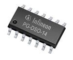
| 供应商器件封装 | PG-DSO-14 |
| 其它名称 | TLE4279GMDKR |
| 包装 | Digi-Reel® |
| 安装类型 | 表面贴装 |
| 封装/外壳 | 14-SOIC(0.154",3.90mm 宽) |
| 工作温度 | -40°C ~ 150°C |
| 标准包装 | 1 |
| 电压-跌落(典型值) | 0.25V @ 100mA |
| 电压-输入 | 最高 45 V |
| 电压-输出 | 5V |
| 电流-输出 | 100mA |
| 电流-限制(最小值) | 150mA |
| 稳压器拓扑 | 正,固定式 |
| 稳压器数 | 1 |


- 商务部:美国ITC正式对集成电路等产品启动337调查
- 曝三星4nm工艺存在良率问题 高通将骁龙8 Gen1或转产台积电
- 太阳诱电将投资9.5亿元在常州建新厂生产MLCC 预计2023年完工
- 英特尔发布欧洲新工厂建设计划 深化IDM 2.0 战略
- 台积电先进制程称霸业界 有大客户加持明年业绩稳了
- 达到5530亿美元!SIA预计今年全球半导体销售额将创下新高
- 英特尔拟将自动驾驶子公司Mobileye上市 估值或超500亿美元
- 三星加码芯片和SET,合并消费电子和移动部门,撤换高东真等 CEO
- 三星电子宣布重大人事变动 还合并消费电子和移动部门
- 海关总署:前11个月进口集成电路产品价值2.52万亿元 增长14.8%


PDF Datasheet 数据手册内容提取
OPTIREG™ Linear TLE4279 5V low drop fixed voltage regulator Features • Output voltage tolerance ≤ ±2% • 150 mA current capability • Very low current consumption • Early warning • Reset output low down to V = 1 V Q • Overtemperature protection • Reverse polarity proof • Adjustable reset threshold • Very low-drop voltage • Wide temperature range • Green Product (RoHS compliant) Potential applications General automotive applications. Product validation Qualified for Automotive Applications. Product Validation according to AEC-Q100/101 Description The OPTIREG™LinearTLE4279 is an automotive voltage regulator with a 5V fixed output, in a PG-DSO-8 or PG-DSO-14 package. The maximum operating voltage is 45V. The output is able to drive 150 mA load. The device features short-circuit protection. The thermal shutdown feature switches the output off when the junction temperature exceeds 150°C to ensure the device is not damaged by overheating. A reset signal is generated when the output voltage drops below V < 4.65V. The reset threshold voltage can be decreased by Q an external connection of a voltage divider. The reset delay time can be set by an external capacitor. If the application requires pull-up resistors at the logic outputs (Reset, Sense Out) the TLE4269 with integrated resistors can be used. It is also possible to supervise the input voltage by using an integrated comparator to give a low voltage warning. Type Package Marking TLE4279G PG-DSO-8 TLE4279 TLE4279GM PG-DSO-14 TLE4279 Data Sheet Rev. 2.5 www.infineon.com 1 2018-11-19
OPTIREG™LinearTLE4279 5V low drop fixed voltage regulator Table of Contents 1 Block diagram . . . . . . . . . . . . . . . . . . . . . . . . . . . . . . . . . . . . . . . . . . . . . . . . . . . . . . . . . . . . . . . . . . . 3 2 Pin configuration . . . . . . . . . . . . . . . . . . . . . . . . . . . . . . . . . . . . . . . . . . . . . . . . . . . . . . . . . . . . . . . . . 4 3 General product characteristics . . . . . . . . . . . . . . . . . . . . . . . . . . . . . . . . . . . . . . . . . . . . . . . . . . . . 6 3.1 Absolute maximum ratings . . . . . . . . . . . . . . . . . . . . . . . . . . . . . . . . . . . . . . . . . . . . . . . . . . . . . . . . . . . . . . . . 6 3.2 Electrical characteristics . . . . . . . . . . . . . . . . . . . . . . . . . . . . . . . . . . . . . . . . . . . . . . . . . . . . . . . . . . . . . . . . . . 8 4 Functional description . . . . . . . . . . . . . . . . . . . . . . . . . . . . . . . . . . . . . . . . . . . . . . . . . . . . . . . . . . . . 9 5 Application description . . . . . . . . . . . . . . . . . . . . . . . . . . . . . . . . . . . . . . . . . . . . . . . . . . . . . . . . . . 10 5.1 Typical performance characteristics . . . . . . . . . . . . . . . . . . . . . . . . . . . . . . . . . . . . . . . . . . . . . . . . . . . . . . . 12 6 Package information . . . . . . . . . . . . . . . . . . . . . . . . . . . . . . . . . . . . . . . . . . . . . . . . . . . . . . . . . . . . . 15 7 Revision History . . . . . . . . . . . . . . . . . . . . . . . . . . . . . . . . . . . . . . . . . . . . . . . . . . . . . . . . . . . . . . . . . 16 Data Sheet 2 Rev. 2.5 2018-11-19
OPTIREG™LinearTLE4279 5V low drop fixed voltage regulator Block diagram 1 Block diagram Ι Q Error Amplifier Reference Current and Saturation Control Trimming D RO & Reference SO RADJ SI AEB01955 Figure1 Block diagram Data Sheet 3 Rev. 2.5 2018-11-19
OPTIREG™LinearTLE4279 5V low drop fixed voltage regulator Pin configuration 2 Pin configuration Ι 1 8 Q SΙ 2 7 SO RADJ 3 6 RO D 4 5 GND AEP01668 Figure2 Pin configuration PG-DSO-8 (top view) Table1 Pin definitions and functions (TLE4279G) Pin No. Symbol Function 1 I Input; block to GND directly at the IC with a ceramic capacitor 2 SI Sense input; if not needed connect to Q 3 RADJ Reset threshold adjust; if not needed connect to ground 4 D Reset delay; to select the delay time, connect to GND via external capacitor 5 GND Ground 6 RO Reset output; open-collector output. Keep open, if not needed 7 SO Sense output; open-collector output. Keep open, if not needed 8 Q 5-V output; connect to GND with a 10 µF capacitor, ESR < 10Ω RADJ 1 14 SI D 2 13 Ι GND 3 12 GND GND 4 11 GND GND 5 10 GND GND 6 9 Q RO 7 8 SO AEP02248 Figure3 Pin configuration PG-DSO-14 (top view) Table2 Pin definitions and functions (TLE4279GM) Pin No. Symbol Function 1 RADJ Reset threshold adjust; if not needed connect to GND 2 D Reset delay; connect to GND via external delay capacitor for setting delay time 3, 4, 5, 6 GND Ground Data Sheet 4 Rev. 2.5 2018-11-19
OPTIREG™LinearTLE4279 5V low drop fixed voltage regulator Pin configuration Table2 Pin definitions and functions (TLE4279GM) (cont’d) Pin No. Symbol Function 7 RO Reset output; open-collector output. Keep open, if not needed 8 SO Sense output; open-collector output. Keep open, if not needed 9 Q 5-V output; connect to GND via 10 µF capacitor, ESR < 10Ω 10, 11, 12 GND Ground 13 I Input; block to GND directly at the IC by a ceramic capacitor 14 SI Sense input; if not needed connect to Q Data Sheet 5 Rev. 2.5 2018-11-19
OPTIREG™LinearTLE4279 5V low drop fixed voltage regulator General product characteristics 3 General product characteristics 3.1 Absolute maximum ratings Table3 Absolute maximum ratings T = -40 to 150 °C j Parameter Symbol Values Unit Note or TestCondition Min. Typ. Max. Input Input voltage V -40 – 45 V – I Input current I – – – – internal limited I Sense input Input voltage V -40 – 45 V – SI Input current I 1 – 1 mA – SI Reset threshold Voltage V -40 – 7 V – RADJ Current I -10 – 10 mA – RADJ Reset delay Voltage V -0.3 – 7 V – D Current I – – – – internal limited D Ground Current I 50 – – mA – GND Reset output Voltage V -0.3 – 7 V – R Current I – – – – internal limited R Sense output Voltage V -0.3 – 7 V – SO Current I – – – – internal limited SO 5-V Output Output voltage V -0.5 – 7 V – Q Output current I -10 – – mA – Q Temperature Junction temperature T – – 150 °C – j Storage temperature T -50 – 150 °C – Stg Data Sheet 6 Rev. 2.5 2018-11-19
OPTIREG™LinearTLE4279 5V low drop fixed voltage regulator General product characteristics Table3 Absolute maximum ratings (cont’d) T = -40 to 150 °C j Parameter Symbol Values Unit Note or TestCondition Min. Typ. Max. Operating range Input voltage V – – 45 V – I Junction temperature T -40 – 150 °C – j Thermal data Junction-ambient R – – 200 K/W PG-DSO-8 thja – 70 K/W PG-DSO-14 Junction-pin R – – 30 K/W PG-DSO-141) thjp 1) measured to Pin 4 Data Sheet 7 Rev. 2.5 2018-11-19
OPTIREG™LinearTLE4279 5V low drop fixed voltage regulator General product characteristics 3.2 Electrical characteristics Table4 Electrical characteristics V = 13.5 V; -40 °C ≤ T ≤ 125 °C I j Parameter Symbol Values Unit Note or TestCondition Min. Typ. Max. Output voltage V 4.90 5.00 5.10 V 1 mA ≤ I ≤ 100 mA Q Q 6 V ≤ V ≤ 16 V I Current limit I 150 200 500 mA – Q Current consumption; I – 150 300 µA I ≤ 1 mA, T < 85 °C q Q j I = I - I q I Q Current consumption; I – 250 700 µA I = 10 mA q Q I = I - I q I Q Current consumption; I – 2 8 mA I = 50 mA q Q I = I - I q I Q Drop voltage V – 0.25 0.5 V I = 100 mA1) dr Q Load regulation ∆V – 10 30 mV I = 5 mA to 100 mA Q Q Line regulation ∆V – 10 40 mV V = 6 V to 26 V Q I I = 1 mA Q Reset generator Switching threshold V 4.50 4.65 4.80 V – RT Reset adjust switching voltage V 1.26 1.35 1.44 V V > 3.5 V RADJ,TH Q Reset low voltage V – 0.1 0.4 V R = 20 kΩ RO,SAT extern Upper delay switching threshold V 1.4 1.8 2.2 V – UD Lower delay switching threshold V 0.3 0.45 0.60 V – LD Reset delay low voltage V – – 0.1 V V < V D,SAT Q RT Charge current I 3.0 6.5 9.5 µA V = 1 V D D Delay time L → H t 17 28 – ms C = 100 nF d D Delay time H → L t – 1 – µs C = 100 nF t D Input voltage sense Sense threshold high V 1.24 1.31 1.38 V – SI, high Sense threshold low V 1.16 1.20 1.28 V – SI, low Sense output low voltage V – 0.1 0.4 V V < 1.20 V; SO, low SI V > 3 V; Q R = 20 kΩ extern Sense input current I -1 0.1 1 µA – SI 1) Drop voltage = V - V (measured when the output voltage has dropped 100mV from the nominal value obtained at I Q 13.5V input.) Data Sheet 8 Rev. 2.5 2018-11-19
OPTIREG™LinearTLE4279 5V low drop fixed voltage regulator Functional description 4 Functional description The control amplifier compares a reference voltage, made highly accurate by resistance balancing, with a voltage proportional to the output voltage and drives the base of the series PNP transistor via a buffer. Saturation control as a function of the load current prevents any over-saturation of the power element. The reset output RO is in high-state if the voltage on the delay capacitor C is greater or equal V . The delay D UD capacitor C is charged with the current I for output voltages greater than the reset threshold V . If the output D D RT voltage gets lower than V (‘reset condition’) a fast discharge of the delay capacitor C sets in and as soon as RT D V gets lower than V the reset output RO is set to low-level. D LD The time gap for the delay capacitor discharge is the reset reaction time t . RR The reset threshold V can be decreased via an external voltage divider connected to the pin RADJ. In this case RT the reset condition is reached if V < V and V <V . Dimensioning the voltage divider (see Figure4) Q RT RADJ RAQDJ,TH according to: (4.1) V × (R +R ) V = -----R---A----D---(--J--,--T---H----)--------------A----D---J--1-------------A----D---J--2---- THRES R ADJ2 the reset threshold can be decreased down to 3.5 V. If the reset-adjust-option is not needed the RADJ-pin should be connected to GND causing the reset threshold to go to its default value (typ. 4.65 V). A built in comparator compares the signal of the pin SI, normally fed by a voltage divider from the input voltage, with the reference and gives an early warning on the pin SO. It is also possible to superwise another voltage e.g. of a second regulator, or to build a watchdog circuit with few external components. Data Sheet 9 Rev. 2.5 2018-11-19
OPTIREG™LinearTLE4279 5V low drop fixed voltage regulator Application information 5 Application information The input capacitor C is necessary for compensating line influences. Using a resistor of approx. 1Ω in series I with C, the oscillating circuit consisting of input inductivity and input capacitance can be damped. The output I capacitor C is necessary for the stability of the regulating circuit. Stability is guaranteed at values ≥ 10µF and Q an ESR ≤ 10Ω within the operating temperature range. Both reset output and sense output are open collector outputs and have to be connected to 5 V output via external pull-up resistors ≥ 10kΩ. For small tolerances of the reset delay the spread of the capacitance of the delay capacitor and its temperature coefficient should be noted. Ι Ι Ι Q Ι Q 1000μ F CΙ TLE 4279 RADJ1 CQ 470 nF 22μ F Ι Ι SΙ RADJ SI RADJ V D GND RO SO V Ι Q Ι Ι V SΙ D GND C V V V V D D RO SO RADJ RADJ2 100 nF AES01956 Figure4 Measuring circuit V I t V <t Q RR V RT t dV I V = D D dt C D V UD V LD t t t RR d V RO V RO, SAT t Power-on-Reset Thermal Voltage Dip Undervoltage Secondary Overload Shutdown at Input Spike at Output AED01542 Figure5 Reset timing diagram Data Sheet 10 Rev. 2.5 2018-11-19
OPTIREG™LinearTLE4279 5V low drop fixed voltage regulator Application information Sense Input Voltage V SI, High V SI, Low t Sense Output High Low t AED03049 Figure6 Sense input timing diagram Data Sheet 11 Rev. 2.5 2018-11-19
OPTIREG™LinearTLE4279 5V low drop fixed voltage regulator Application information 5.1 Typical performance characteristics Charge current I versus Drop voltage V versus D dr temperature T output current I J Q 16 AED01803 500 AED01805 ΙD μ A Vdr mV 14 V =13.5 V Ι V =1.0 V 400 C 12 10 300 8 T =125 C j 200 6 T = 25 C j 4 100 2 0 0 -40 0 40 80 120 C 160 0 30 60 90 120 mA 180 T Ι j Q Switching voltage V and V versus Reset adjust switching threshold V versus UD LD RADJ,TH temperature T temperature T j j 3.2 AED01804 1.7 AED01806 V V V V D RADJ, TH 2.8 1.6 V =13.5 V Ι 2.4 1.5 2.0 VUD 1.4 1.6 1.3 1.2 1.2 0.8 1.1 V LD 0.4 1.0 0 0.9 -40 0 40 80 120 C 160 -40 0 40 80 120 C 160 T T j j Data Sheet 12 Rev. 2.5 2018-11-19
OPTIREG™LinearTLE4279 5V low drop fixed voltage regulator Application information Current consumption I versus Sense threshold V versus Q SI input voltage V temperature T I j 30 AED01807 1.6 AED01809 Ι V q mA SI V V =13.5 V Ι 25 1.5 20 1.4 R = 33 Ω Sense Output High L 15 1.3 Sense Output Low 10 1.2 R = 50 Ω L 5 R =100 Ω 1.1 L R = 200 Ω L 0 1.0 0 10 20 30 40 V 50 -40 0 40 80 120 C 160 V T Ι j Output voltage V versus Output voltage V versus Q Q input voltage V temperature T I j 12 AED01808 5.2 AED01671 V V Q V Q V 10 5.1 V =13.5 V Ι 8 5.0 6 4.9 R = 50 Ω L 4 4.8 2 4.7 0 4.6 0 2 4 6 8 V 10 -40 0 40 80 120 C 160 V T Ι j Data Sheet 13 Rev. 2.5 2018-11-19
OPTIREG™LinearTLE4279 5V low drop fixed voltage regulator Application information Output current I versus Current consumption I versus Q q input voltage V output current I I Q 350 AED01810 1.6 AED01812 Ι Ι mA Q mA q 1.4 300 V =13.5 V Ι T = 25 C j 1.2 250 1.0 T = 25 C j 200 0.8 150 T =125 C j 0.6 100 0.4 50 0.2 0 0 0 10 20 30 40 V 50 0 10 20 30 40 mA 50 V Ι Ι Q Current consumption I versus q output current I Q 12 AED01811 Ι q mA 10 V =13.5 V Ι T = 25 C j 8 6 4 2 0 0 20 40 60 80 mA 120 Ι Q Data Sheet 14 Rev. 2.5 2018-11-19
OPTIREG™LinearTLE4279 5V low drop fixed voltage regulator Package information 6 Package information 0.35 x 45° 0.175 ±0.07 (1.45) 1.75 MAX. 4-0.20.191+0.0)6 MAX.8° 1.27 B 0.1 0.64±0.25 0.41+0.1 -0.06 0.2M AB 8x 6±0.2 8 5 Index Marking 1 4 A 5 1) -0.2 1) Does not include plastic or metal protrusion of 0.15 max. per side 2) Lead width can be 0.61 max. in dambar area GPS01229 Figure7 PG-DSO-8 (Plastic Dual Small Outline)1) Figure8 PG-DSO-14 Green Product (RoHS compliant) To meet the world-wide customer requirements for environmentally friendly products and to be compliant with government regulations the device is available as a green product. Green products are RoHS-Compliant (i.e Pb-free finish on leads and suitable for Pb-free soldering according to IPC/JEDEC J-STD-020). Further information on packages https://www.infineon.com/packages 1) Dimensions in mm Data Sheet 15 Rev. 2.5 2018-11-19
OPTIREG™LinearTLE4279 5V low drop fixed voltage regulator Revision history 7 Revision history Revision Date Changes 2.5 2018-11-19 Updated package drawing “PG-DSO-14” Editorial changes 2.4 2007-03-20 Initial version of RoHS-compliant derivate of TLE4279 Page 1: AEC certified statement added Page1 and 15: RoHS compliance statement and Green product feature added Package changed to RoHS compliant version Legal disclaimer updated Data Sheet 16 Rev. 2.5 2018-11-19
Trademarks All referenced product or service names and trademarks are the property of their respective owners. IMPORTANT NOTICE Edition 2018-11-19 The information given in this document shall in no For further information on technology, delivery terms event be regarded as a guarantee of conditions or and conditions and prices, please contact the nearest Published by characteristics ("Beschaffenheitsgarantie"). Infineon Technologies Office (www.infineon.com). Infineon Technologies AG With respect to any examples, hints or any typical 81726 Munich, Germany values stated herein and/or any information regarding the application of the product, Infineon Technologies WARNINGS hereby disclaims any and all warranties and liabilities © 2018 Infineon Technologies AG. of any kind, including without limitation warranties of Due to technical requirements products may contain All Rights Reserved. non-infringement of intellectual property rights of any dangerous substances. For information on the types third party. in question please contact your nearest Infineon In addition, any information given in this document is Technologies office. Do you have a question about any subject to customer's compliance with its obligations aspect of this document? stated in this document and any applicable legal Except as otherwise explicitly approved by Infineon Email: erratum@infineon.com requirements, norms and standards concerning Technologies in a written document signed by customer's products and any use of the product of authorized representatives of Infineon Technologies, Infineon Technologies in customer's applications. Infineon Technologies’ products may not be used in The data contained in this document is exclusively any applications where a failure of the product or any Document reference intended for technically trained staff. It is the consequences of the use thereof can reasonably be Z8F55294584 responsibility of customer's technical departments to expected to result in personal injury. evaluate the suitability of the product for the intended application and the completeness of the product information given in this document with respect to such application.
Mouser Electronics Authorized Distributor Click to View Pricing, Inventory, Delivery & Lifecycle Information: I nfineon: TLE4279GM