ICGOO在线商城 > TLE4270-2G
 Datasheet下载
- 型号: TLE4270-2G
- 制造商: Infineon
- 库位|库存: xxxx|xxxx
- 要求:
| 数量阶梯 | 香港交货 | 国内含税 |
| +xxxx | $xxxx | ¥xxxx |
查看当月历史价格
查看今年历史价格
TLE4270-2G产品简介:
ICGOO电子元器件商城为您提供TLE4270-2G由Infineon设计生产,在icgoo商城现货销售,并且可以通过原厂、代理商等渠道进行代购。 提供TLE4270-2G价格参考¥10.88-¥14.37以及InfineonTLE4270-2G封装/规格参数等产品信息。 你可以下载TLE4270-2G参考资料、Datasheet数据手册功能说明书, 资料中有TLE4270-2G详细功能的应用电路图电压和使用方法及教程。
| 参数 | 数值 |
| 产品目录 | 集成电路 (IC)半导体 |
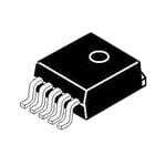
| 描述 | IC REG LDO 5V 0.55A TO263-5低压差稳压器 LW Drop Fixed VOLT REGULATOR 200mA 5V |
| 产品分类 | |
| 品牌 | Infineon Technologies |
| 产品手册 | http://www.infineon.com/dgdl/TLE4270-2_DS_18.pdf?folderId=db3a304314dca3890115039cf70d0bf0&fileId=db3a3043163797a601163915ad4d01c9 |
| 产品图片 |
|
| rohs | 符合RoHS无铅 / 符合限制有害物质指令(RoHS)规范要求 |
| 产品系列 | 电源管理 IC,低压差稳压器,Infineon Technologies TLE4270-2G- |
| 数据手册 | http://www.infineon.com/dgdl/Infineon-TLE4270_2-DS-v01_08-en.pdf?folderId=db3a304318f3fe290118f5a433570040&fileId=db3a30431b3e89eb011ba19cb0ff0bd9&ack=t |
| 产品型号 | TLE4270-2G |
| 产品目录页面 | |
| 产品种类 | 低压差稳压器 |
| 供应商器件封装 | PG-TO263-5 |
| 其它名称 | TLE4270-2GDKR |
| 包装 | Digi-Reel® |
| 商标 | Infineon Technologies |
| 回动电压—最大值 | 700 mV at 550 mA |
| 安装类型 | 表面贴装 |
| 安装风格 | SMD/SMT |
| 封装 | Reel |
| 封装/外壳 | TO-263-6,D²Pak(5 引线+接片),TO-263BA |
| 封装/箱体 | TO-263-5 |
| 工作温度 | -40°C ~ 150°C |
| 工厂包装数量 | 1000 |
| 最大工作温度 | + 150 C |
| 最大输入电压 | 42 V |
| 最小工作温度 | - 40 C |
| 最小输入电压 | + 6 V |
| 标准包装 | 1 |
| 电压-跌落(典型值) | 0.35V @ 550mA |
| 电压-输入 | 6 V ~ 42 V |
| 电压-输出 | 5V |
| 电压调节准确度 | 2% |
| 电流-输出 | 550mA |
| 电流-限制(最小值) | 650mA |
| 稳压器拓扑 | 正,固定式 |
| 稳压器数 | 1 |
| 系列 | TLE4270 |
| 线路调整率 | 25 mV |
| 负载调节 | 50 mV |
| 输出电压 | 5 V |
| 输出电流 | 650 mA |
| 输出端数量 | 1 Output |
| 输出类型 | Fixed |
| 零件号别名 | SP000304929 TLE42702GATMA1 |


PDF Datasheet 数据手册内容提取
5-V Low Drop Fixed Voltage Regulator TLE 4270-2 Features • Output voltage tolerance ≤ ±2% (cid:127) 650 mA output cu rrent capability (cid:127) Low-drop voltage (cid:127) Reset functionality (cid:127) Adjustable reset time (cid:127) Suitable for use in automotive electronics (cid:127) Integrated overtemperature protection (cid:127) Reverse polarity protection (cid:127) Input voltage up to 42 V (cid:127) Overvoltage protection up to 65 V ( ≤ 400 ms) (cid:127) Short-circuit proof (cid:127) Wide temperature range P-TO252-5-1 (cid:127) ESD protection: ±2kV HBM1) (cid:127) Green Product (RoHS compliant) (cid:127) AEC Qualified Functional Description This device is a 5-V low drop fixed-voltage regulator. The maximum input voltage is 42 V (65 V, ≤ 400 ms). Up to an input voltage of 26 V and for an output current up to 650 mA it regulates the output voltage within a 2% accuracy. The short circuit protection limits the output current of more than 650 mA. The device incorporates overvoltage protection and a temperature protection which turns off the device at high temperatures. 1) ESD susceptibility, Human Body Model (HBM) according to EIA/JESD 22-A114B Type Package TLE 4270-2 G PG-TO263-5-1 TLE 4270-2 D PG-TO252-5-11 Data Sheet 1 Rev. 1.8, 2007-11-09
TLE 4270-2 PG-TO263-5-1 PG-TO252-5 GND 1 5 1 5 RO D Ι GND Q Ι RO D Q AEP02580 AEP01922 Figure 1 Pin Configuration (top view) Table 1 Pin Definitions and Functions Pin Symbol Function 1 I Input; block to ground directly at the IC with a ceramic capacitor. 2 RO Reset Output; the open collector output is connected to the 5-V output via an integrated resistor of 30 kΩ. 3 GND Ground; internally connected to heatsink. 4 D Reset Delay; connect a capacitor to ground for delay time adjustment. 5 Q 5-V Output; block to ground with 22 µF capacitor, ESR < 3 Ω. Data Sheet 2 Rev. 1.8, 2007-11-09
TLE 4270-2 Circuit Description The control amplifier compares a reference voltage, which is kept highly accurate by resistance adjustment, to a voltage that is proportional to the output voltage and drives the base of a series transistor via a buffer. Saturation control as a function of the load current prevents any over-saturation of the power element. The IC also incorporates a number of internal circuits for protection against: (cid:127) Overload (cid:127) Overvoltage (cid:127) Overtemperature (cid:127) Reverse polarity Application Description The IC regulates an input voltage in the range of 5.5 V < V < 36 V to V = 5.0 V. Up I Q,nom to 26 V it produces a regulated output current of more than 650 mA. Above 26 V the save-operating-area protection allows operation up to 36 V with a regulated output current of more than 300 mA. Overvoltage protection limits operation at 42 V. The overvoltage protection hysteresis restores operation if the input voltage has dropped below 36 V. A reset signal is generated for an output voltage of V < 4.5 V. The delay for Q power-on reset can be set externally with a capacitor. Data Sheet 3 Rev. 1.8, 2007-11-09
TLE 4270-2 Temperature Saturation Sensor Control and Protection Circuit 1 5 I Q Control Amplifier Buffer Bandgap Reset 2 Reference RO Generator 4 D Adjustment 3 GND AEB01924 Figure 2 Block Diagram Data Sheet 4 Rev. 1.8, 2007-11-09
TLE 4270-2 Table 2 Absolute Maximum Ratings T = -40 to 150 °C j Parameter Symbol Limit Values Unit Notes Min. Max. Input I Voltage V -42 42 V – I Voltage V – 65 V t ≤ 400 ms I Current I – – – internally limited I Reset Output RO Voltage V -0.3 7 V – RO Current I – – – Internally limited RO Reset Delay D Voltage V -0.3 7 V – D Current I – – – Internally limited D Output Q Voltage V -1.0 16 V – Q Current I – – – Internally limited Q Ground GND Current I -0.5 – A – GND Temperatures Junction temperature T – 150 °C – j Storage temperature T -50 150 °C – stg Table 3 Operating Range Parameter Symbol Limit Values Unit Notes Min. Max. Input voltage V 6 42 V – I Junction temperature T -40 150 °C – j Thermal Resistance Junction ambient R – 65 K/W – thj-a 79 K/W TO263, TO2521) Junction case R – 3 K/W TO-263 Packages thj-c 1) Mounted on PCB, 80 × 80 × 1.5 mm3; 35µ Cu; 5µ Sn; Footprint only; zero airflow. Data Sheet 5 Rev. 1.8, 2007-11-09
TLE 4270-2 Table 4 Characteristics V = 13.5 V; -40 °C ≤ T ≤ 125 °C (unless otherwise specified) I j Parameter Symbol Limit Values Unit Test Condition Min. Typ. Max. Output voltage V 4.90 5.00 5.10 V 5 mA ≤ I ≤ 550 mA; Q Q 6 V ≤ V ≤ 26 V I Output voltage V 4.90 5.00 5.10 V 26 V ≤ V ≤ 36 V; Q I I ≤ 300 mA Q Output current I 650 850 – mA V = 0 V Qmax Q limiting Current I – 1 1.5 mA I = 5 mA q Q consumption I = I - I q I Q Current I – 55 75 mA I = 550 mA q Q consumption I = I - I q I Q Current I – 70 90 mA I = 550 mA; V = 5 V q Q I consumption I = I - I q I Q Drop voltage V – 350 700 mV I = 550 mA1) DR Q Load regulation ∆V – 25 50 mV I = 5 to 550 mA; Q,Lo Q V = 6 V I Line regulation ∆V – 12 25 mV V = 6 to 26 V Q,Li I I = 5 mA Q Power supply Ripple PSRR – 54 – dB f = 100 Hz; r rejection V = 0.5 Vpp r Reset Generator Switching threshold V 4.5 4.65 4.8 V – RT Reset High voltage V 4.5 – – V – ROH Reset low voltage V – 60 – mV R = 30 kΩ2); ROL int 1.0 V ≤ V ≤ 4.5 V Q Reset low voltage V – 200 400 mV I = 3 mA, V = 4.4 V ROL R Q Reset pull-up R 18 30 46 kΩ internally connected int to Q Charge current I 8 14 25 µA V = 1.0 V D,c D Data Sheet 6 Rev. 1.8, 2007-11-09
TLE 4270-2 Table 4 Characteristics (cont’d) V = 13.5 V; -40 °C ≤ T ≤ 125 °C (unless otherwise specified) I j Parameter Symbol Limit Values Unit Test Condition Min. Typ. Max. Upper reset timing V 1.4 1.8 2.3 V – DU threshold Lower reset timing V 0.2 0.45 0.8 V V < V DL Q RT threshold Delay time t – 13 – ms C = 100 nF rd D Reset reaction time t – – 3 µs C = 100 nF rr D Overvoltage Protection Turn-Off voltage V 42 44 46 V – I, ov 1) Drop voltage = V - V (measured when the output voltage has dropped 100 mV from the nominal value I Q obtained at 13.5 V input) 2) Reset peak is always lower than 1.0 V. Data Sheet 7 Rev. 1.8, 2007-11-09
TLE 4270-2 I I I I Q Q 1 5 1000 µF 470 nF 22 µF TTLLEE 44227700-G2 I R RO 2 V 4 3 V I Q D GND V I R D I GND V D C D AES01925 Figure 3 Test Circuit I 1 5 Q Input 5 V - Output 470 nF TLE 4270 TLE4270-2 Reset RO D 2 4 22 µF to µC 3 GND 100 nF AES01926 Figure 4 Application Circuit Data Sheet 8 Rev. 1.8, 2007-11-09
TLE 4270-2 Design Notes for External Components An input capacitor C is necessary for compensation of line influences. The resonant I circuit consisting of lead inductance and input capacitance can be damped by a resistor of approx. 1 Ω in series with C. An output capacitor C is necessary for the stability of I Q the regulating circuit. Stability is guaranteed at values of C ≥ 22 µF and an ESR of Q < 3 Ω. Reset Circuitry If the output voltage decreases below 4.5 V, an external capacitor C on pin 4 (D) will be D discharged by the reset generator. If the voltage on this capacitor drops below V , a DL reset signal is generated on pin 2 (RO), i.e. reset output is set low. If the output voltage rises above the reset threshold, C will be charged with constant current. After the D power-on-reset time the voltage on the capacitor reaches V and the reset output will DU be set high again. The value of the power-on-reset time can be set within a wide range depending of the capacitance of C . D Reset Timing The power-on reset delay time is defined by the charging time of an external capacitor C which can be calculated as follows: D C = (∆t × I )/∆V (1) D D,c Definitions: (cid:127) C = delay capacitors D (cid:127) ∆t = reset delay time t rd (cid:127) I = charge current, typical 14 µA D,c (cid:127) ∆V = V , typical 1.8 V DU V = upper reset timing threshold at C for reset delay time DU D t = ∆V × C /I (2) rd D D,c The reset reaction time t is the time it takes the voltage regulator to set the reset out rr LOW after the output voltage has dropped below the reset threshold. It is typically 1 µs for delay capacitor of 47 nF. For other values for C the reaction time can be estimated D using the following equation: t ≈ 20 s/F × C (3) rr D Data Sheet 9 Rev. 1.8, 2007-11-09
TLE 4270-2 V I <t rr V V RT Q dV ID, c = dt C D V DU VD VDL t t rr rd V RO Power-ON Thermal Voltage Drop Under- Secondary Load Reset Shutdown at Input voltage Spike Bounce AES01927 Figure 5 Reset Time Response Data Sheet 10 Rev. 1.8, 2007-11-09
TLE 4270-2 Output Voltage V versus Output Voltage V versus Q Q Temperature T Input Voltage V j I AED01928 AED01929 5.2 12 V V V Q V Q 5.1 10 V = 13.5 V I 5.0 8 4.9 6 R = 25Ω L 4.8 4 4.7 2 4.6 0 -40 0 40 80 120 ˚C160 0 2 4 6 8 V 10 T j VΙ Output Current I versus Output Current I versus Q Q Temperature T Input Voltage V j I 1200 AED01930 1.2 AED03038 mA I I A Q max Q 1000 1.0 800 0.8 T = 125 ˚C 600 0.6 j 25 ˚C 400 0.4 200 0.2 0 0 -40 0 40 80 120 ˚C160 0 10 20 30 40 V 50 T V j I Data Sheet 11 Rev. 1.8, 2007-11-09
TLE 4270-2 Current Consumption I versus Current Consumption I versus q q Output Current I Output Current I Q Q AED03092 AED03093 3 80 mA Ι mA Ι q q 70 60 2 50 40 V = 13.5 V Ι 30 1 V = 13.5 V Ι 20 10 0 0 0 20 40 60 80 mA 120 0 100 200 300 400 mA 600 Ι Ι Q Q Current Consumption I versus Drop Voltage V versus q DR Input Voltage V Output Current I I Q 120 AED01934 800 AED01935 mV I mA V q DR700 100 600 80 500 T = 125 ˚C j R = 10Ω 25 ˚C L 60 400 300 40 R = 20Ω 200 L 50Ω 20 100 0 0 0 10 20 30 40 V 50 0 200 400 600 mA 1000 V I I Q Data Sheet 12 Rev. 1.8, 2007-11-09
TLE 4270-2 Charge Current I versus Upper Reset Timing Threshold V D,c DU Temperature T versus Temperature T j j AED03094 AED03047 4.0 20 mA µA V I DU 3.5 18 16 3.0 I D, c 14 2.5 V = 13.5 V Ι V = 13.5 V 12 I 2.0 V = 1 V D V DU 10 1.5 8 1.0 6 0.5 4 0 -40 0 40 80 120 ˚C160 -40 0 40 80 120 ˚C 160 T j T j Data Sheet 13 Rev. 1.8, 2007-11-09
TLE 4270-2 Package Outlines 4.4 10±0.2 1.27±0.1 0...0.3 A B 8.51) 3 0.05 0. ± 1 2.4 2 1) ±0. 55 0.1 5) 25 7. (1 9. 7±0.5 2.7±0.3 4. 0...0.15 5 x 0.8±0.1 0.5±0.1 4 x 1.7 8˚ MAX. 0.25 M A B 0.1 B 1) Typical Metal surface min. X = 7.25, Y = 6.9 All metal surfaces tin plated, except area of cut. GPT09113 GPT09113 Figure 6 PG-TO263-5-1 (Plastic Transistor Single Outline) Green Product (RoHS compliant) To meet the world-wide customer requirements for environmentally friendly products and to be compliant with government regulations the device is available as a green product. Green products are RoHS-Compliant (i.e Pb-free finish on leads and suitable for Pb-free soldering according to IPC/JEDEC J-STD-020). You can find all of our packages, sorts of packing and others in our Infineon Internet Page “Products”: http://www.infineon.com/products. SMD = Surface Mounted Device Dimensions in mm Data Sheet 14 Rev. 1.8, 2007-11-09
TLE 4270-2 6.5+0.15 -0.05 A 5.7 MAX.1) 2.3-+00..1005 (5) B 0.5+0.08 1 -0.04 0. ± 1 0.9+0.20 0.5 -0.2 24) ±0.15 0...0-0.1.051 9.98± 6.22 (4. 0.8 N. MI 1 0.15 MAX. 5 0. per side 5 x 0.6±0.1 0.5-+00..0048 1.14 0.1 B 4.56 0.25 M A B 1) Includes mold flashes on each side. All metal surfaces tin plated, except area of cut. GPT09527 Figure 7 PG-TO252-5-11 (Plastic Transistor Single Outline) Green Product (RoHS compliant) To meet the world-wide customer requirements for environmentally friendly products and to be compliant with government regulations the device is available as a green product. Green products are RoHS-Compliant (i.e Pb-free finish on leads and suitable for Pb-free soldering according to IPC/JEDEC J-STD-020). You can find all of our packages, sorts of packing and others in our Infineon Internet Page “Products”: http://www.infineon.com/products. SMD = Surface Mounted Device Dimensions in mm Data Sheet 15 Rev. 1.8, 2007-11-09
TLE 4270-2 Revision History Revision History Version Date Changes Rev. 1.8 2007-11-09 Page 1: Changed ESD specification from “>4000V” to “±2kV HBM” according to PCN No. 2007-089 Rev. 1.7 2007-03-20 Initial version of RoHS-compliant derivate of TLE 4270 Change of product name to TLE 4270-2 due to modified chip layout and size. Page 1: AEC certified statement added Page 1 and Page 14: RoHS compliance statement and Green product feature added Page 1 and Page 14: Package changed to RoHS compliant version Legal Disclaimer updated Data Sheet 16 Rev. 1.8, 2007-11-09
Edition 2007-11-09 Published by Infineon Technologies AG 81726 Munich, Germany © 2007 Infineon Technologies AG All Rights Reserved. Legal Disclaimer The information given in this document shall in no event be regarded as a guarantee of conditions or characteristics. With respect to any examples or hints given herein, any typical values stated herein and/or any information regarding the application of the device, Infineon Technologies hereby disclaims any and all warranties and liabilities of any kind, including without limitation, warranties of non-infringement of intellectual property rights of any third party. Information For further information on technology, delivery terms and conditions and prices, please contact the nearest Infineon Technologies Office (www.infineon.com). Warnings Due to technical requirements, components may contain dangerous substances. For information on the types in question, please contact the nearest Infineon Technologies Office. Infineon Technologies components may be used in life-support devices or systems only with the express written approval of Infineon Technologies, if a failure of such components can reasonably be expected to cause the failure of that life-support device or system or to affect the safety or effectiveness of that device or system. Life support devices or systems are intended to be implanted in the human body or to support and/or maintain and sustain and/or protect human life. If they fail, it is reasonable to assume that the health of the user or other persons may be endangered.
Mouser Electronics Authorized Distributor Click to View Pricing, Inventory, Delivery & Lifecycle Information: I nfineon: TLE4270 TLE4270G TLE4270S TLE4270-2D TLE4270-2S TLE4270-2 TLE4270-2G