ICGOO在线商城 > TLE4251D
 Datasheet下载
- 型号: TLE4251D
- 制造商: Infineon
- 库位|库存: xxxx|xxxx
- 要求:
| 数量阶梯 | 香港交货 | 国内含税 |
| +xxxx | $xxxx | ¥xxxx |
查看当月历史价格
查看今年历史价格
TLE4251D产品简介:
ICGOO电子元器件商城为您提供TLE4251D由Infineon设计生产,在icgoo商城现货销售,并且可以通过原厂、代理商等渠道进行代购。 提供TLE4251D价格参考以及InfineonTLE4251D封装/规格参数等产品信息。 你可以下载TLE4251D参考资料、Datasheet数据手册功能说明书, 资料中有TLE4251D详细功能的应用电路图电压和使用方法及教程。
| 参数 | 数值 |
| 产品目录 | 集成电路 (IC) |
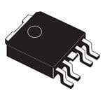
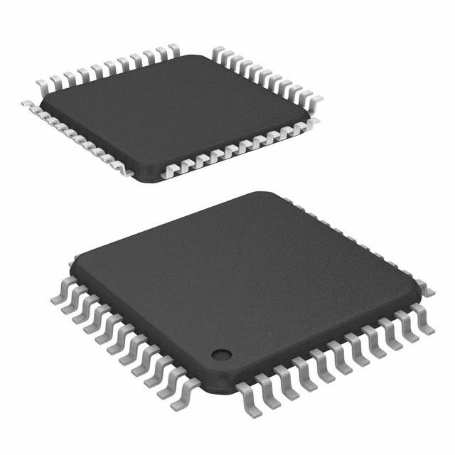
| 描述 | IC REG LDO ADJ 0.4A DPAK |
| 产品分类 | |
| 品牌 | Infineon Technologies |
| 数据手册 | http://www.infineon.com/dgdl/TLE4251_DS_29.pdf?folderId=db3a304412b407950112b408e8c90004&fileId=db3a304412b407950112b435489262ae |
| 产品图片 |
|
| 产品型号 | TLE4251D |
| rohs | 无铅 / 符合限制有害物质指令(RoHS)规范要求 |
| 产品系列 | - |
| 产品目录页面 | |
| 供应商器件封装 | PG-TO252-5 |
| 其它名称 | TLE4251DINDKR |
| 包装 | Digi-Reel® |
| 安装类型 | 表面贴装 |
| 封装/外壳 | TO-252-5,DPak(4 引线 + 接片),TO-252AD |
| 工作温度 | -40°C ~ 150°C |
| 标准包装 | 1 |
| 电压-跌落(典型值) | 0.28V @ 300mA |
| 电压-输入 | 4 V ~ 40 V |
| 电压-输出 | 可调 |
| 电流-输出 | 400mA |
| 电流-限制(最小值) | - |
| 稳压器拓扑 | 正,可调式 |
| 稳压器数 | 1 |
.jpg)


.jpg)


- 商务部:美国ITC正式对集成电路等产品启动337调查
- 曝三星4nm工艺存在良率问题 高通将骁龙8 Gen1或转产台积电
- 太阳诱电将投资9.5亿元在常州建新厂生产MLCC 预计2023年完工
- 英特尔发布欧洲新工厂建设计划 深化IDM 2.0 战略
- 台积电先进制程称霸业界 有大客户加持明年业绩稳了
- 达到5530亿美元!SIA预计今年全球半导体销售额将创下新高
- 英特尔拟将自动驾驶子公司Mobileye上市 估值或超500亿美元
- 三星加码芯片和SET,合并消费电子和移动部门,撤换高东真等 CEO
- 三星电子宣布重大人事变动 还合并消费电子和移动部门
- 海关总署:前11个月进口集成电路产品价值2.52万亿元 增长14.8%


PDF Datasheet 数据手册内容提取
Low Drop Voltage Tracker TLE 4251 Features • Output tracking tolerance ≤ ±0.2% (cid:129) 400 mA output cu rrent capability (cid:129) Enable Function (cid:129) Very low current cons umption in OFF mode (cid:129) Wide operation range: up to 40 V (cid:129) Wide temperature range: -40 °C ≤ T ≤ 150 °C P-TO252-5-11 j (cid:129) Output protected against short circuit (cid:129) Overtemperature protection (cid:129) Reverse polarity proof (cid:129) Green Product (RoHS compliant) (cid:129) AEC Qualified Functional Description The TLE 4251 is a monolithic integrated low drop voltage tracker in the very small SMD package PG-TO252-5-1. It P-TO263-5-1 is designed to supply e.g. sensors under the severe conditions of automotive applications. Therefore the device is equipped with additional protection functions against overload, short circuit and reverse polarity. Supply voltages up to 40 V are tracked to a reference voltage given to the adjust input via an external resistor. The output is able to drive loads up to 400 mA while it follows e.g. the 5 V output of a main voltage regulator within an accuracy of 0.5%. For loads up to 300 mA the tracking accuracy is 0.2%. The TLE 4251 can be switched in stand-by mode via the enable EN input which causes the current consumption to drop to very low values. This feature makes the IC suitable for low power battery applications. Type Package TLE 4251 D PG-TO252-5-11 TLE 4251 G PG-TO263-5-1 Data Sheet 1 Rev. 2.9, 2007-03-20
TLE 4251 PG-TO263-5-1 PG-TO252-5-11 GND 1 5 1 5 I EN ADJ Q AEP02810 I EN GND ADJ Q AEP03119 Figure 1 Pin Configuration (top view) Table 1 Pin Definitions and Functions Pin No. Symbol Function 1 I Input voltage 2 EN Enable; high-active input 3 GND Ground 4 ADJ Adjust; connect directly to the reference or with a voltage divider to the reference (for reference-proportional output voltages, VQ<Vref)….. 5 Q Output voltage; must be blocked by a capacitor C ≥ 22 μF, ESR ≤ 3 Ω to GND Q Data Sheet 2 Rev. 2.9, 2007-03-20
TLE 4251 TLE 4251 Saturation Control and Temperature Protection Control Circuit I ADJ EN GND AES02807 Figure 2 Block Diagram Data Sheet 3 Rev. 2.9, 2007-03-20
TLE 4251 Table 2 Absolute Maximum Ratings -40 °C < T < 150 °C j Parameter Symbol Limit Values Unit Remarks Min. Max. Input Voltage V -42 45 V – I Current I – – mA internally limited I Output Voltage V -2 45 V – Q Current I – – mA internally limited Q Adjust Voltage V -42 45 V – ADJ Current I – – μA internally limited ADJ Enable Voltage V -42 45 V – EN Current I – – μA internally limited EN Temperatures Junction temperature T -40 150 °C – j Storage temperature T -50 150 °C – stg Thermal Resistances Junction case R – 4 K/W TLE 4251 D thjc Junction ambient R – 78 K/W TLE 4251 D1) thja Junction case R – 3 K/W TLE 4251 G thjc Junction ambient R – 52 K/W TLE 4251 G1) thja 1) Worst case, regarding peak temperature; zero airflow; mounted an a PCB 80 × 80 × 1.5 mm3, heat sink area 300mm2. Note: Maximum ratings are absolute ratings; exceeding any one of these values may cause irreversible damage to the integrated circuit. Data Sheet 4 Rev. 2.9, 2007-03-20
TLE 4251 Table 3 Operating Range Parameter Symbol Limit Values Unit Remarks Min. Max. Input voltage V 41) 40 V – I Adjust input voltage V 2.5 40 V – ADJ Adjust input voltage V 0 2.5 V V ≤ V + ΔV ADJ Q ADJ Q Enable input voltage V 0 40 V – EN Junction temperature T -40 150 °C – j 1) V > V + V I ADJ DR Data Sheet 5 Rev. 2.9, 2007-03-20
TLE 4251 Table 4 Electrical Characteristics V = 13.5 V; 2.5 V ≤ V ≤ V - 0.5 V; -40 °C < T < 150 °C; unless otherwise specified I ADJ I j Parameter Symbol Limit Values Unit Test Condition Min. Typ. Max. Output Output voltage tracking ΔV -10 – 10 mV V < 13.5 V; Q I accuracy -40 °C < T < 125 °C; j ΔV = V - V 1 mA < I < 300 mA Q ADJ Q Q Output voltage tracking ΔV -10 – 10 mV 6 V < V < 40 V; Q I accuracy 5 mA < I < 200 mA Q Output voltage tracking ΔV -25 – 25 mV 6 V < V < 28 V; Q I accuracy 1 mA < I < 300 mA Q Drop voltage V – 280 520 mV I = 300 mA; dr Q V > 4 V; ADJ Enable ON1) Output current I 400 450 800 mA T ≤ 125 °C1) Q j Output capacitor C 22 – – μF ESR ≤ 3 Ω at 10 kHz Q Current consumption I – 10 20 mA I = 300 mA q Q I = I - I q I Q Current consumption I – 230 300 μA I < 1 mA; T < 85 °C; q Q j I = I - I V in ON state q I Q EN Quiescent current I – 0 2 μA V = 0 V; T < 85 °C q EN j (stand-by) I = I - I q I Q Regulator Performance Load regulation ΔV -35 ±5 35 mV 5 mA < I < 300 mA; Q Q V = 6 V; V = 5 V I ADJ Line regulation ΔV -25 ±10 25 mV 12 V < V < 32 V; Q I I = 5 mA Q Power Supply Ripple PSRR 60 – – dB f = 100 Hz; r Rejection V = 0.5 Vpp; r V = 5 V; ADJ C = 22 μF Tantalum Q Adjust Input Input biasing current I – 0.1 0.5 μA V = 5 V ADJ ADJ Data Sheet 6 Rev. 2.9, 2007-03-20
TLE 4251 Table 4 Electrical Characteristics (cont’d) V = 13.5 V; 2.5 V ≤ V ≤ V - 0.5 V; -40 °C < T < 150 °C; unless otherwise specified I ADJ I j Parameter Symbol Limit Values Unit Test Condition Min. Typ. Max. Enable Enable on voltage range V 2 – – V V ON EN ON Q Enable off voltage range V – – 0.5 V V ≤ 0.1 V EN OFF Q Input current I 5 40 70 μA V = 5 V EN EN 1) Measured when the output voltage V has dropped 100 mV from the nominal value. Q Application Information e.g. TLE 4470 µC 6...40 V TLE 4269 I Q V TLE 4278 CC GND 100 nF 22 µF I/O TLE 4251 Saturation Control and Temperature Protection Control Circuit I LOAD Q to sensor 22 µF 100 nF ADJ C EN 100 nF GND AES02808 Figure 3 Application Circuit Data Sheet 7 Rev. 2.9, 2007-03-20
TLE 4251 Quiescent Current I versus Enable Current I versus q EN Output Current I Enable Voltage V Q EN AED02900 AED02901 30 30 µA I mA I q ENABLE 25 25 20 20 15 15 10 10 5 5 0 0 0 100 200 300 mA 450 0 0.5 1 1.5 2 2.5 3 3.5 V4 I V Q ENABLE Tracking Accuracy ΔV versus Current Consumption I versus Q q Temperature T, V = 5 V Input Voltage V, V = 5 V j ADJ I ADJ AED02902 AED02904 6 400 mV V I µA Q q 4 350 V = 6 V I I = 300 mA Q 2 300 0 I = 10 mA Q 250 -2 V = 40 V I IQ= 200 mA IQ= 1 mA 200 -4 -6 150 -40 0 40 80 120 ˚C 160 0 5 10 15 20 25 30 35 V 45 T V j Ι Data Sheet 8 Rev. 2.9, 2007-03-20
TLE 4251 Tracking Accuracy ΔV versus Q Output Current I Q AED02903 3 mV V Q 2.5 V = 5 V ADJ 2 V = 3 V ADJ 1.5 1 0.5 0 0 100 200 300 400mA500 I Q Data Sheet 9 Rev. 2.9, 2007-03-20
TLE 4251 Package Outlines 6.5+0.15 -0.05 A 5.7 MAX.1) 2.3-+00..1005 (5) B 0.5+0.08 1 -0.04 0. ± 1 0.9+0.20 0.5 -0.2 24) ±0.15 0...0-0.1.051 9.98± 6.22 (4. 0.8 N. MI 1 0.15 MAX. 5 0. per side 5 x 0.6±0.1 0.5-+00..0048 1.14 0.1 B 4.56 0.25 M A B 1) Includes mold flashes on each side. All metal surfaces tin plated, except area of cut. GPT09527 Figure 4 PG-TO252-5-11 (Plastic Transistor Single Outline) Green Product (RoHS compliant) To meet the world-wide customer requirements for environmentally friendly products and to be compliant with government regulations the device is available as a green product. Green products are RoHS-Compliant (i.e Pb-free finish on leads and suitable for Pb-free soldering according to IPC/JEDEC J-STD-020). You can find all of our packages, sorts of packing and others in our Infineon Internet Page “Products”: http://www.infineon.com/products. SMD = Surface Mounted Device Dimensions in mm Data Sheet 10 Rev. 2.9, 2007-03-20
TLE 4251 4.4 10±0.2 1.27±0.1 0...0.3 A B 8.51) 3 0.05 0. ± 1 2.4 2 1) ±0. 55 0.1 5) 25 7. (1 9. 7±0.5 2.7±0.3 4. 0...0.15 5 x 0.8±0.1 0.5±0.1 4 x 1.7 8˚ MAX. 0.25 M A B 0.1 B 1) Typical Metal surface min. X = 7.25, Y = 6.9 All metal surfaces tin plated, except area of cut. GPT09113 GPT09113 Figure 5 PG-TO263-5-1 (Plastic Transistor Single Outline) Green Product (RoHS compliant) To meet the world-wide customer requirements for environmentally friendly products and to be compliant with government regulations the device is available as a green product. Green products are RoHS-Compliant (i.e Pb-free finish on leads and suitable for Pb-free soldering according to IPC/JEDEC J-STD-020). You can find all of our packages, sorts of packing and others in our Infineon Internet Page “Products”: http://www.infineon.com/products. SMD = Surface Mounted Device Dimensions in mm Data Sheet 11 Rev. 2.9, 2007-03-20
TLE 4251 Revision History Revision History Version Date Changes Rev. 2.9 2007-03-20 Initial version of RoHS-compliant derivate of TLE 4251 Page 1: AEC certified statement added Page 1 and Page 10: RoHS compliance statement and Green product feature added Page 1 and Page 10: Package changed to RoHS compliant version Legal Disclaimer updated Data Sheet 12 Rev. 2.9, 2007-03-20
Edition 2007-03-20 Published by Infineon Technologies AG 81726 Munich, Germany © 2007 Infineon Technologies AG All Rights Reserved. Legal Disclaimer The information given in this document shall in no event be regarded as a guarantee of conditions or characteristics. With respect to any examples or hints given herein, any typical values stated herein and/or any information regarding the application of the device, Infineon Technologies hereby disclaims any and all warranties and liabilities of any kind, including without limitation, warranties of non-infringement of intellectual property rights of any third party. Information For further information on technology, delivery terms and conditions and prices, please contact the nearest Infineon Technologies Office (www.infineon.com). Warnings Due to technical requirements, components may contain dangerous substances. For information on the types in question, please contact the nearest Infineon Technologies Office. Infineon Technologies components may be used in life-support devices or systems only with the express written approval of Infineon Technologies, if a failure of such components can reasonably be expected to cause the failure of that life-support device or system or to affect the safety or effectiveness of that device or system. Life support devices or systems are intended to be implanted in the human body or to support and/or maintain and sustain and/or protect human life. If they fail, it is reasonable to assume that the health of the user or other persons may be endangered.
Mouser Electronics Authorized Distributor Click to View Pricing, Inventory, Delivery & Lifecycle Information: I nfineon: TLE4251GXT TLE4251D TLE4251G