ICGOO在线商城 > TLE2061CD
 Datasheet下载
- 型号: TLE2061CD
- 制造商: Texas Instruments
- 库位|库存: xxxx|xxxx
- 要求:
| 数量阶梯 | 香港交货 | 国内含税 |
| +xxxx | $xxxx | ¥xxxx |
查看当月历史价格
查看今年历史价格
TLE2061CD产品简介:
ICGOO电子元器件商城为您提供TLE2061CD由Texas Instruments设计生产,在icgoo商城现货销售,并且可以通过原厂、代理商等渠道进行代购。 提供TLE2061CD价格参考¥5.56-¥5.56以及Texas InstrumentsTLE2061CD封装/规格参数等产品信息。 你可以下载TLE2061CD参考资料、Datasheet数据手册功能说明书, 资料中有TLE2061CD详细功能的应用电路图电压和使用方法及教程。
| 参数 | 数值 |
| -3db带宽 | - |
| 产品目录 | 集成电路 (IC)半导体 |
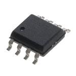
| 描述 | IC OPAMP JFET 2MHZ 8SOIC运算放大器 - 运放 Low Power JFET |
| 产品分类 | Linear - Amplifiers - Instrumentation, OP Amps, Buffer Amps集成电路 - IC |
| 品牌 | Texas Instruments |
| 产品手册 | |
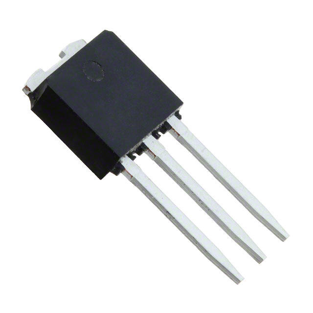
| 产品图片 |
|
| rohs | 符合RoHS无铅 / 符合限制有害物质指令(RoHS)规范要求 |
| 产品系列 | 放大器 IC,运算放大器 - 运放,Texas Instruments TLE2061CDExcalibur™ |
| 数据手册 | |
| 产品型号 | TLE2061CD |
| 产品目录页面 | |
| 产品种类 | 运算放大器 - 运放 |
| 供应商器件封装 | 8-SOIC |
| 共模抑制比—最小值 | 65 dB |
| 关闭 | No Shutdown |
| 其它名称 | 296-10393-5 |
| 包装 | 管件 |
| 单位重量 | 76 mg |
| 压摆率 | 3.4 V/µs |
| 双重电源电压 | +/- 5 V, +/- 9 V, +/- 12 V, +/- 15 V |
| 商标 | Texas Instruments |
| 增益带宽生成 | 1.8 MHz |
| 增益带宽积 | 2MHz |
| 安装类型 | 表面贴装 |
| 安装风格 | SMD/SMT |
| 封装 | Tube |
| 封装/外壳 | 8-SOIC(0.154",3.90mm 宽) |
| 封装/箱体 | SOIC-8 |
| 工作温度 | 0°C ~ 70°C |
| 工作电源电压 | +/- 3.5 V to +/- 18 V |
| 工厂包装数量 | 75 |
| 技术 | BiFET |
| 放大器类型 | J-FET |
| 最大双重电源电压 | +/- 18 V |
| 最大工作温度 | + 70 C |
| 最小双重电源电压 | +/- 3.5 V |
| 最小工作温度 | 0 C |
| 标准包装 | 75 |
| 电压-电源,单/双 (±) | 7 V ~ 36 V, ±3.5 V ~ 18 V |
| 电压-输入失调 | 600µV |
| 电流-电源 | 290µA |
| 电流-输入偏置 | 4pA |
| 电流-输出/通道 | 80mA |
| 电源电流 | 0.35 mA |
| 电路数 | 1 |
| 系列 | TLE2061 |
| 转换速度 | 3.4 V/us |
| 输入偏压电流—最大 | 3 nA |
| 输入参考电压噪声 | 59 nV |
| 输入补偿电压 | 3.1 mV |
| 输出类型 | - |
| 通道数量 | 1 Channel |


- 商务部:美国ITC正式对集成电路等产品启动337调查
- 曝三星4nm工艺存在良率问题 高通将骁龙8 Gen1或转产台积电
- 太阳诱电将投资9.5亿元在常州建新厂生产MLCC 预计2023年完工
- 英特尔发布欧洲新工厂建设计划 深化IDM 2.0 战略
- 台积电先进制程称霸业界 有大客户加持明年业绩稳了
- 达到5530亿美元!SIA预计今年全球半导体销售额将创下新高
- 英特尔拟将自动驾驶子公司Mobileye上市 估值或超500亿美元
- 三星加码芯片和SET,合并消费电子和移动部门,撤换高东真等 CEO
- 三星电子宣布重大人事变动 还合并消费电子和移动部门
- 海关总署:前11个月进口集成电路产品价值2.52万亿元 增长14.8%


PDF Datasheet 数据手册内容提取
(cid:1)(cid:1) (cid:2)(cid:3)(cid:4)(cid:5)(cid:6)(cid:7)(cid:8)(cid:9) (cid:2)(cid:3)(cid:4)(cid:5)(cid:6)(cid:7)(cid:8)(cid:10)(cid:9) (cid:2)(cid:3)(cid:4)(cid:5)(cid:6)(cid:7)(cid:8)(cid:11) (cid:4)(cid:12)(cid:13)(cid:10)(cid:3)(cid:14)(cid:11)(cid:15)(cid:16) (cid:17)(cid:18)(cid:4)(cid:2)(cid:19)(cid:14)(cid:20)(cid:21)(cid:15)(cid:2) (cid:22)(cid:14)(cid:23)(cid:22)(cid:19)(cid:24)(cid:15)(cid:2)(cid:21)(cid:15)(cid:2)(cid:19)(cid:25)(cid:16)(cid:14)(cid:26)(cid:4) µ(cid:21)(cid:24)(cid:27)(cid:4)(cid:16) (cid:24)(cid:21)(cid:4)(cid:16)(cid:10)(cid:2)(cid:14)(cid:24)(cid:20)(cid:10)(cid:3) (cid:10)(cid:28)(cid:21)(cid:3)(cid:14)(cid:18)(cid:14)(cid:4)(cid:16)(cid:29) SLOS193B − FEBRUARY 1997 − REVISED MAY 2004 (cid:1) 2× Bandwidth (2 MHz) of the TL06x and (cid:1) High Output Drive, Specified into 100-Ω TL03x Operational Amplifiers Loads (cid:1) Low Supply Current ... 290 µA/Ch Typ (cid:1) Lower Noise Floor Than Earlier (cid:1) On-chip Offset Voltage Trimming for Generations of Low-Power BiFETs Improved DC Performance description The TLE206x series of low-power JFET-input operational amplifiers doubles the bandwidth of the earlier generation TL06x and TL03x BiFET families without significantly increasing power consumption. Texas Instruments Excalibur process also delivers a lower noise floor than the TL06x and TL03x. On-chip zener trimming of offset voltage yields precision grades for dc-coupled applications. The TL206x devices are pin-compatible with other Texas Instruments BiFETs; they can be used to double the bandwidth of TL06x and TL03x circuits or to reduce power consumption of TL05x, TL07x, and TL08x circuits by nearly 90%. BiFET operational amplifiers offer the inherently-higher input impedance of the JFET-input transistors, without sacrificing the output drive associated with bipolar amplifiers. This makes them better suited for interfacing with high-impedance sensors or low-level ac signals. They also feature inherently better ac response than bipolar or CMOS devices having comparable power consumption. The TLE206x family features a high-output-drive circuit capable of driving 100-Ω loads at supplies as low as ±5 V. This makes them uniquely suited for driving transformer loads in modems and other applications requiring good ac characteristics, low power, and high output drive. Because BiFET operational amplifiers are designed for use with dual power supplies, care must be taken to observe common-mode input voltage limits and output swing when operating from a single supply. DC biasing of the input signal is required and loads should be terminated to a virtual ground node at mid-supply. Texas Instruments TLE2426 integrated virtual ground generator is useful when operating BiFET amplifiers from single supplies. The TLE206x are fully specified at ±15 V and ±5 V. For operation in low-voltage and/or single-supply systems, Texas Instruments LinCMOS families of operational amplifiers (TLC- and TLV-prefixes) are recommended. When moving from BiFET to CMOS amplifiers, particular attention should be paid to slew rate and bandwidth requirements and output loading. The Texas Instruments TLV2432 and TLV2442 CMOS operational amplifiers are excellent choices to consider. Please be aware that an important notice concerning availability, standard warranty, and use in critical applications of TexasInstruments semiconductor products and disclaimers thereto appears at the end of this data sheet. (cid:21)(cid:16)(cid:24)(cid:25)(cid:15)(cid:13)(cid:2)(cid:14)(cid:24)(cid:20) (cid:25)(cid:10)(cid:2)(cid:10) (cid:30)(cid:31)!"#$%&(cid:30)"(cid:31) (cid:30)’ ()##*(cid:31)& %’ "! +),-(cid:30)(%&(cid:30)"(cid:31) .%&*/ Copyright 2004, Texas Instruments Incorporated (cid:21)#".)(&’ ("(cid:31)!"#$ &" ’+*((cid:30)!(cid:30)(%&(cid:30)"(cid:31)’ +*# &0* &*#$’ "! (cid:2)*(cid:8)%’ (cid:14)(cid:31)’&#)$*(cid:31)&’ ’&%(cid:31).%#. 1%##%(cid:31)&2/ (cid:21)#".)(&(cid:30)"(cid:31) +#"(*’’(cid:30)(cid:31)3 ."*’ (cid:31)"& (cid:31)*(*’’%#(cid:30)-2 (cid:30)(cid:31)(-).* &*’&(cid:30)(cid:31)3 "! %-- +%#%$*&*#’/ POST OFFICE BOX 655303 • DALLAS, TEXAS 75265 1
(cid:2)(cid:3)(cid:4)(cid:5)(cid:6)(cid:7)(cid:8)(cid:9) (cid:2)(cid:3)(cid:4)(cid:5)(cid:6)(cid:7)(cid:8)(cid:10)(cid:9) (cid:2)(cid:3)(cid:4)(cid:5)(cid:6)(cid:7)(cid:8)(cid:11) (cid:1) (cid:4)(cid:12)(cid:13)(cid:10)(cid:3)(cid:14)(cid:11)(cid:15)(cid:16) (cid:17)(cid:18)(cid:4)(cid:2)(cid:19)(cid:14)(cid:20)(cid:21)(cid:15)(cid:2) (cid:22)(cid:14)(cid:23)(cid:22)(cid:19)(cid:24)(cid:15)(cid:2)(cid:21)(cid:15)(cid:2)(cid:19)(cid:25)(cid:16)(cid:14)(cid:26)(cid:4) µ(cid:21)(cid:24)(cid:27)(cid:4)(cid:16) (cid:24)(cid:21)(cid:4)(cid:16)(cid:10)(cid:2)(cid:14)(cid:24)(cid:20)(cid:10)(cid:3) (cid:10)(cid:28)(cid:21)(cid:3)(cid:14)(cid:18)(cid:14)(cid:4)(cid:16)(cid:29) SLOS193B − FEBRUARY 1997 − REVISED MAY 2004 TLE2061 AVAILABLE OPTIONS PACKAGED DEVICES TA AVTIO 2m5a°Cx OSUMTLAILNLE† CACRHRIPIER CERDAIPMIC PLADSIPTIC TS(PSWOP)‡ FCLEART APMACICK (D) (FK) (JG) (P) (U) 500 µV — — — — — — 00°CC ttoo 7700°CC 1.5 mV TLE2061ACD — — TLE2061ACP — — 3 mV TLE2061CD — — TLE2061CP TLE2061CPWLE — 500 µV — — — — — — −−4400°CC ttoo 8855°CC 1.5 mV TLE2061AID — — TLE2061AIP — — 3 mV TLE2061ID — — TLE2061IP — — 500 µV — — TLE2061BMJG — — — −−5555°CC ttoo 112255°CC 1.5 mV TLE2061AMD TLE2061AMFK TLE2061AMJG — — TLE2061AMU 3 mV TLE2061MD TLE2061MFK TLE2061MJG — — TLE2061MU †The D packages are available taped and reeled. Add R suffix to device type (e.g., TLE2061ACDR).Chips are tested at 25°C. ‡The PW package is available left-end taped and reeled (indicated by the LE suffix on the device type (e.g., TLE2061CPWLE). TLE2062 AVAILABLE OPTIONS PACKAGED DEVICES CERAMIC VIOmax SMALL OUTLINE† CHIP CARRIER CERAMIC DIP PLASTIC DIP TA AT 25°C (D) (FK) (JG) (P) FLAT PACK (U) 0°C 1 mV TLE2062BCD — — TLE2062BCP — to 2 mV TLE2062ACD — — TLE2062ACP — 70°C 4 mV TLE2062CD — — TLE2062CP — −40°C 1 mV TLE2062BID — — TLE2062BIP — to 2 mV TLE2062AID — — TLE2062AIP — 85°C 4 mV TLE2062ID — — TLE2062IP — −55°C 1 mV TLE2062BMD — TLE2062BMJG — — to 2 mV TLE2062AMD TLE2062AMFK TLE2062AMJG — TLE2062AMU 125°C 4 mV TLE2062MD TLE2062MFK TLE2062MJG — TLE2062MU †The D packages are available taped and reeled. Add R suffix to device type (e.g., TLE2062ACDR). TLE2064 AVAILABLE OPTIONS PACKAGED DEVICES CCEERRAAMMIICC VVIIOOmmaaxx SSMMAALLLL OOUUTTLLIINNEE†† CCHHIIPP CCAARRRRIIEERR CCEERRAAMMIICC DDIIPP PPLLAASSTTIICC DDIIPP TTAA AATT 2255°°CC ((DD)) ((FFKK)) ((JJ)) ((NN)) FFLLAATT PPAACCKK (W) 0°C 2 mV — TLE2064BCN to 4 mV TLE2064ACD — — TLE2064ACN — 70°C 6 mV TLE2064CD TLE2064CN −40°C 2 mV — TLE2064BIN to 4 mV TLE2064AID — — TLE2064AIN — 85°C 6 mV TLE2064ID TLE2064IN −55°C 2 mV — TLE2064BMFK TLE2064BMJ — to 4 mV TLE2064AMD TLE2064AMFK TLE2064AMJ — TLE2064AMW 125°C 6 mV TLE2064MD TLE2064MFK TLE2064MJ TLE2064MW †The D packages are available taped and reeled. Add R suffix to device type, (e.g., TLE2064ACDR). 2 POST OFFICE BOX 655303 • DALLAS, TEXAS 75265
(cid:1) (cid:2)(cid:3)(cid:4)(cid:5)(cid:6)(cid:7)(cid:8)(cid:9) (cid:2)(cid:3)(cid:4)(cid:5)(cid:6)(cid:7)(cid:8)(cid:10)(cid:9) (cid:2)(cid:3)(cid:4)(cid:5)(cid:6)(cid:7)(cid:8)(cid:11) (cid:4)(cid:12)(cid:13)(cid:10)(cid:3)(cid:14)(cid:11)(cid:15)(cid:16) (cid:17)(cid:18)(cid:4)(cid:2)(cid:19)(cid:14)(cid:20)(cid:21)(cid:15)(cid:2) (cid:22)(cid:14)(cid:23)(cid:22)(cid:19)(cid:24)(cid:15)(cid:2)(cid:21)(cid:15)(cid:2)(cid:19)(cid:25)(cid:16)(cid:14)(cid:26)(cid:4) µ(cid:21)(cid:24)(cid:27)(cid:4)(cid:16) (cid:24)(cid:21)(cid:4)(cid:16)(cid:10)(cid:2)(cid:14)(cid:24)(cid:20)(cid:10)(cid:3) (cid:10)(cid:28)(cid:21)(cid:3)(cid:14)(cid:18)(cid:14)(cid:4)(cid:16)(cid:29) SLOS193B − FEBRUARY 1997 − REVISED MAY 2004 TLE2064, TLE2064A, TLE2064B D, J, N, OR W PACKAGE TLE2061, TLE2061A, AND TLE2061B TLE2062, TLE2062A, TLE2062B (TOP VIEW) D, JG, OR P PACKAGE D, DB, JG, P, OR PW PACKAGE (TOP VIEW) (TOP VIEW) 1OUT 1 14 4OUT 1IN− 2 13 4IN− OFFSET N1 1 8 NC 1OUT 1 8 VCC+ 1IN+ 3 12 4IN+ IN− 2 7 VCC+ 1IN− 2 7 2OUT VCC+ 4 11 VCC− IN+ 3 6 OUT 1IN+ 3 6 2IN− 2IN+ 5 10 3IN+ VCC− 4 5 OFFSET N2 VCC− 4 5 2IN+ 2IN− 6 9 3IN− 2OUT 7 8 3OUT TLE2061M, TLE2061AM, TLE2061BM TLE2062M, TLE2062AM, TLE2062BM TLE2064M, TLE2064AM, TLE2064BM FK PACKAGE FK PACKAGE FK PACKAGE (TOP VIEW) (TOP VIEW) (TOP VIEW) SET N1 NC 1OUT NCVCC +NC 1IN − 1OUT NC4OUT 4IN − F C F CC C 3 2 1 20 19 N O NN N NC 43 2 1 20 1918 NC 1IN+ 4 18 4IN+ 3 2 1 20 19 1IN− 5 17 2OUT NC 5 17 NC NC 4 18 NC NC 6 16 NC VCC+ 6 16 VCC− IN− 5 17 VCC+ 1IN+ 7 15 2IN− NC 7 15 NC NC 6 16 NC NC 8 14 NC 2IN+ 8 14 3IN+ IN+ 7 15 OUT 9 10 11 12 13 9 10 11 12 13 NC 8 14 NC − T CT − C9 1−0C11212C13 NC VCC − NC2IN+ NC 2IN 2OU N3OU 3IN N CNN N VC ET S F F O TLE2061 AND TLE2061A TLE2062 AND TLE2062A U PACKAGE U PACKAGE (TOP VIEW) (TOP VIEW) NC 1 10 NC NC 1 10 NC OFFSET N1 2 9 NC 1OUT 2 9 VCC+ IN− 3 8 VCC+ 1IN− 3 8 2OUT IN+ 4 7 OUT 1IN+ 4 7 2IN− VCC− 5 6 OFFSET N2 VCC− 5 6 2IN+ NC − No internal connection POST OFFICE BOX 655303 • DALLAS, TEXAS 75265 3
Template Release Date: 7−11−94 (cid:2)(cid:3)(cid:4)(cid:5)(cid:6)(cid:7)(cid:8)(cid:9)4(cid:2)(cid:3)(cid:4)(cid:5)(cid:6)(cid:7)(cid:8)(cid:10)(cid:9)4(cid:2)(cid:3)(cid:4)(cid:5)(cid:6)(cid:7)(cid:8)(cid:11) (cid:4)(cid:12)(cid:13)(cid:10)(cid:3)(cid:14)(cid:11)(cid:15)(cid:16)4(cid:17)(cid:18)(cid:4)(cid:2)(cid:19)(cid:14)(cid:20)(cid:21)(cid:15)(cid:2)4(cid:22)(cid:14)(cid:23)(cid:22)(cid:19)(cid:24)(cid:15)(cid:2)(cid:21)(cid:15)(cid:2)(cid:19)(cid:25)(cid:16)(cid:14)(cid:26)(cid:4) µ(cid:21)(cid:24)(cid:27)(cid:4)(cid:16)4(cid:24)(cid:21)(cid:4)(cid:16)(cid:10)(cid:2)(cid:14)(cid:24)(cid:20)(cid:10)(cid:3)4(cid:10)(cid:28)(cid:21)(cid:3)(cid:14)(cid:18)(cid:14)(cid:4)(cid:16)(cid:29) SLOS193B − FEBRUARY 1997 − REVISED APRIL 2004 T U O 2 Ω Q4 R9 00 1 Ω 8 R 0 2 1 4 Q 9 0 3 4 Q Q 5 7 8 3 6 3 3 Q 3 Q Q Q 2 4 D 2 3 3 3 3 Q Q Q 1 D Q30 Q31 9 7Ω Q2 R0 0 6 4 Q27 E206 42 9 2 3 8 L 2 T Q 6 2 T Q25 23 Q UN Q O 4 C 2 VCC+ R6 Ω2.7 k Q2 VCC− ONENT TLE206 42 9 2 3 Q18 Q19 Q17 20 21 22 es. OMP Q Q Q c C evi E 61 d C 0 Q16 61x EVI LE2 43 9 1 3 3 0 D T Q1 Q14 1 F Q15 Q12 he TLE2 CTUAL T channel) Q9 Q7Q1 Q10C3R35.3 pΩ2.4 k C2Q815 pF R2R5ΩΩ1.1 k60 k T N2 are only availiable on tminal. A COMPONEN Transistors Resistors Diodes Capacitors matic (each Q4 Q5Q3 Q6 C1 15 pF 2 R4Ω55 k 2See Note A N1 AND OFFSEnt values are no ent sche IN+ IN−Q1 Q R1Ω1.1 k OFFSET NFFSET N1 A.OFFSET B.Compone al O v S: ui TE q O e N 4 POST OFFICE BOX 655303 • DALLAS, TEXAS 75265
(cid:1) (cid:2)(cid:3)(cid:4)(cid:5)(cid:6)(cid:7)(cid:8)(cid:9) (cid:2)(cid:3)(cid:4)(cid:5)(cid:6)(cid:7)(cid:8)(cid:10)(cid:9) (cid:2)(cid:3)(cid:4)(cid:5)(cid:6)(cid:7)(cid:8)(cid:11) (cid:4)(cid:12)(cid:13)(cid:10)(cid:3)(cid:14)(cid:11)(cid:15)(cid:16) (cid:17)(cid:18)(cid:4)(cid:2)(cid:19)(cid:14)(cid:20)(cid:21)(cid:15)(cid:2) (cid:22)(cid:14)(cid:23)(cid:22)(cid:19)(cid:24)(cid:15)(cid:2)(cid:21)(cid:15)(cid:2)(cid:19)(cid:25)(cid:16)(cid:14)(cid:26)(cid:4) µ(cid:21)(cid:24)(cid:27)(cid:4)(cid:16) (cid:24)(cid:21)(cid:4)(cid:16)(cid:10)(cid:2)(cid:14)(cid:24)(cid:20)(cid:10)(cid:3) (cid:10)(cid:28)(cid:21)(cid:3)(cid:14)(cid:18)(cid:14)(cid:4)(cid:16)(cid:29) SLOS193B − FEBRUARY 1997 − REVISED MAY 2004 absolute maximum ratings over operating free-air temperature range (unless otherwise noted)† Supply voltage, V (see Note 1) . . . . . . . . . . . . . . . . . . . . . . . . . . . . . . . . . . . . . . . . . . . . . . . . . . . . . . . . . . . 19 V CC+ Supply voltage, V . . . . . . . . . . . . . . . . . . . . . . . . . . . . . . . . . . . . . . . . . . . . . . . . . . . . . . . . . . . . . . . . . . . . . −19 V CC− Differential input voltage, V (see Note 2) . . . . . . . . . . . . . . . . . . . . . . . . . . . . . . . . . . . . . . . . . . . . . . . . . . . ±38 V ID Input voltage range, V (any input) . . . . . . . . . . . . . . . . . . . . . . . . . . . . . . . . . . . . . . . . . . . . . . . . . . . . . . . . . . . ±V I CC Input current, I (each input) . . . . . . . . . . . . . . . . . . . . . . . . . . . . . . . . . . . . . . . . . . . . . . . . . . . . . . . . . . . . . . . ±1 mA I Output current, I . . . . . . . . . . . . . . . . . . . . . . . . . . . . . . . . . . . . . . . . . . . . . . . . . . . . . . . . . . . . . . . . . . . . . . . ±80 mA O Total current into V . . . . . . . . . . . . . . . . . . . . . . . . . . . . . . . . . . . . . . . . . . . . . . . . . . . . . . . . . . . . . . . . . . . 80 mA CC+ Total current out of V . . . . . . . . . . . . . . . . . . . . . . . . . . . . . . . . . . . . . . . . . . . . . . . . . . . . . . . . . . . . . . . . −80 mA CC− Duration of short-circuit current at (or below) 25°C (see Note 3) . . . . . . . . . . . . . . . . . . . . . . . . . . . . . unlimited Package thermal impedance, θ (see Notes 4 and 5): D package (8-pin) . . . . . . . . . . . . . . . . . . . . 97.1°C/W JA D package (14-pin) . . . . . . . . . . . . . . . . . . 86.2°C/W N package . . . . . . . . . . . . . . . . . . . . . . . . . . 79.7°C/W P package . . . . . . . . . . . . . . . . . . . . . . . . . . 84.6°C/W PW package . . . . . . . . . . . . . . . . . . . . . . . . . 113°C/W Package thermal impedance, θ (see Notes 4 and 5): FK package . . . . . . . . . . . . . . . . . . . . . . . . . . . 5.6°C/W JC J package . . . . . . . . . . . . . . . . . . . . . . . . . . 15.1°C/W JG package . . . . . . . . . . . . . . . . . . . . . . . . . 14.5°C/W U package . . . . . . . . . . . . . . . . . . . . . . . . . . 14.7°C/W W package . . . . . . . . . . . . . . . . . . . . . . . . . . . 10°C/W Operating free-air temperature range, T : C suffix . . . . . . . . . . . . . . . . . . . . . . . . . . . . . . . . . . . . . . 0°C to 70°C A I suffix . . . . . . . . . . . . . . . . . . . . . . . . . . . . . . . . . . . . . −40°C to 85°C M suffix . . . . . . . . . . . . . . . . . . . . . . . . . . . . . . . . . . −55°C to 125°C Storage temperature range . . . . . . . . . . . . . . . . . . . . . . . . . . . . . . . . . . . . . . . . . . . . . . . . . . . . . . . −65°C to 150°C Case temperature for 60 seconds: FK package . . . . . . . . . . . . . . . . . . . . . . . . . . . . . . . . . . . . . . . . . . . . . . 260°C Lead temperature 1,6 mm (1/16 inch) from case for 10 seconds: D, P, or PW package . . . . . . . . . . . . 260°C Lead temperature 1,6 mm (1/16 inch) from case for 60 seconds: JG, U, or W package . . . . . . . . . . . . 300°C †Stresses beyond those listed under “absolute maximum ratings” may cause permanent damage to the device. These are stress ratings only, and functional operation of the device at these or any other conditions beyond those indicated under “recommended operating conditions” is not implied. Exposure to absolute-maximum-rated conditions for extended periods may affect device reliability. NOTES: 1. All voltage values, except differential voltages, are with respect to the midpoint between VCC+ and VCC−. 2. Differential voltages are at IN+ with respect to IN−. 3. The output may be shorted to either supply. Temperature and/or supply voltages must be limited to ensure that the maximum dissipation rating is not exceeded. θ 4. Maximum power dissipation is a function of TJ(max), JA, and TA. The maximum allowable power dissipation at any allowable ambient temperature is PD = (TJ(max) − TA)/θJA. Operating at the absolute maximum TJ of 150°C can affect reliability. 5. The package thermal impedance is calculated in accordance with JESD 51-7 (plastic) or MIL-STD-883 Method 1012 (ceramic). recommended operating conditions C SUFFIX I SUFFIX M SUFFIX UUNNIITT MIN MAX MIN MAX MIN MAX Supply voltage, VCC(cid:1)± ±3.5 ±18 ±3.5 ±18 ±3.5 ±18 V VCC±= ±(cid:1)5 V −1.6 4 −1.6 4 −1.6 4 CCoommmmoonn--mmooddee iinnppuutt vvoollttaaggee,, VVIICC VCC±= ±(cid:1)15 V −11 13 −11 13 −11 13 VV Operating free-air temperature, TA 0 70 −40 85 −55 125 °C POST OFFICE BOX 655303 • DALLAS, TEXAS 75265 5
(cid:2)(cid:3)(cid:4)(cid:5)(cid:6)(cid:7)(cid:8)(cid:9) (cid:2)(cid:3)(cid:4)(cid:5)(cid:6)(cid:7)(cid:8)(cid:10)(cid:9) (cid:2)(cid:3)(cid:4)(cid:5)(cid:6)(cid:7)(cid:8)(cid:11) (cid:1) (cid:4)(cid:12)(cid:13)(cid:10)(cid:3)(cid:14)(cid:11)(cid:15)(cid:16) (cid:17)(cid:18)(cid:4)(cid:2)(cid:19)(cid:14)(cid:20)(cid:21)(cid:15)(cid:2) (cid:22)(cid:14)(cid:23)(cid:22)(cid:19)(cid:24)(cid:15)(cid:2)(cid:21)(cid:15)(cid:2)(cid:19)(cid:25)(cid:16)(cid:14)(cid:26)(cid:4) µ(cid:21)(cid:24)(cid:27)(cid:4)(cid:16) (cid:24)(cid:21)(cid:4)(cid:16)(cid:10)(cid:2)(cid:14)(cid:24)(cid:20)(cid:10)(cid:3) (cid:10)(cid:28)(cid:21)(cid:3)(cid:14)(cid:18)(cid:14)(cid:4)(cid:16)(cid:29) SLOS193B − FEBRUARY 1997 − REVISED MAY 2004 TLE2061C electrical characteristics at specified free-air temperature, VCC± = ±5 V (unless otherwise noted) TLE2061C TLE2061AC PARAMETER TEST CONDITIONS TTAA† TLE2061BC UNIT MIN TYP MAX 25°C 0.8 3.1 TTLLEE22006611CC Full range 4 25°C 0.6 2.6 VVIIOO IInnppuutt ooffffsseett vvoollttaaggee TTLLEE22006611AACC mmVV Full range 3.5 25°C 0.5 1.9 TTLLEE22006611BBCC Full range 2.4 αVIO Temperature coefficient of input offset voltage VVIICC == 00,, RRSS == 5500 ΩΩ Full range 6 µV/°C Input offset voltage long-term drift (see Note 4) 25°C 0.04 µV/mo 25°C 1 pA IIIIOO IInnppuutt ooffffsseett ccuurrrreenntt Full range 0.8 nA 25°C 3 pA IIIIBB IInnppuutt bbiiaass ccuurrrreenntt Full range 2 nA −1.6 −2 25°C to to V 4 6 VVIICCRR CCoommmmoonn--mmooddee iinnppuutt vvoollttaaggee rraannggee −1.6 Full range to V 4 25°C 3.5 3.7 RRLL == 1100 kkΩΩ Full range 3.3 VVOOMM++ MMaaxxiimmuumm ppoossiittiivvee ppeeaakk oouuttppuutt vvoollttaaggee sswwiinngg 25°C 2.5 3.1 VV RRLL == 110000 ΩΩ Full range 2 25°C −3.7 −3.9 RRLL == 1100 kkΩΩ Full range −3.3 VVOOMM−− MMaaxxiimmuumm nneeggaattiivvee ppeeaakk oouuttppuutt vvoollttaaggee sswwiinngg 25°C −2.5 −2.7 VV RRLL == 110000 ΩΩ Full range −2 25°C 15 80 VVOO == ±±22..88 VV,, RRLL == 1100 kkΩΩ Full range 2 25°C 0.75 45 AAVVDD LLaarrggee--ssiiggnnaall ddiiffffeerreennttiiaall vvoollttaaggee aammpplliiffiiccaattiioonn VVOO == 00 ttoo 22 VV,, RRLL == 110000 ΩΩ VV//mmVV Full range 0.5 25°C 0.5 3 VVOO == 00 ttoo −−22 VV,, RRLL == 110000 ΩΩ Full range 0.25 ri Input resistance 25°C 1012 Ω ci Input capacitance 25°C 4 pF zo Open-loop output impedance IO = 0 25°C 280 Ω 25°C 65 82 CCMMRRRR CCoommmmoonn--mmooddee rreejjeeccttiioonn rraattiioo VVIICC == VVIICCRRmmiinn,, RRSS == 5500 ΩΩ ddBB Full range 65 kkSSVVRR SSuuppppllyy--vvoollttaaggee rreejjeeccttiioonn rraattiioo ((∆∆VVCCCC±//∆∆VVIIOO)) VVRCCSCC =±± 5 ==0 ±±Ω55 VV ttoo ±±1155 VV,, Fu2ll 5r°aCnge 7755 93 ddBB †Full range is 0°C to 70°C. NOTE 6: Typical values are based on the input offset voltage shift observed through 168 hours of operating life test at TA = 150°C extrapolated to TA = 25°C using the Arrhenius equation and assuming an activation energy of 0.96 eV. 6 POST OFFICE BOX 655303 • DALLAS, TEXAS 75265
(cid:1) (cid:2)(cid:3)(cid:4)(cid:5)(cid:6)(cid:7)(cid:8)(cid:9) (cid:2)(cid:3)(cid:4)(cid:5)(cid:6)(cid:7)(cid:8)(cid:10)(cid:9) (cid:2)(cid:3)(cid:4)(cid:5)(cid:6)(cid:7)(cid:8)(cid:11) (cid:4)(cid:12)(cid:13)(cid:10)(cid:3)(cid:14)(cid:11)(cid:15)(cid:16) (cid:17)(cid:18)(cid:4)(cid:2)(cid:19)(cid:14)(cid:20)(cid:21)(cid:15)(cid:2) (cid:22)(cid:14)(cid:23)(cid:22)(cid:19)(cid:24)(cid:15)(cid:2)(cid:21)(cid:15)(cid:2)(cid:19)(cid:25)(cid:16)(cid:14)(cid:26)(cid:4) µ(cid:21)(cid:24)(cid:27)(cid:4)(cid:16) (cid:24)(cid:21)(cid:4)(cid:16)(cid:10)(cid:2)(cid:14)(cid:24)(cid:20)(cid:10)(cid:3) (cid:10)(cid:28)(cid:21)(cid:3)(cid:14)(cid:18)(cid:14)(cid:4)(cid:16)(cid:29) SLOS193B − FEBRUARY 1997 − REVISED MAY 2004 TLE2061C electrical characteristics at specified free-air temperature, VCC± = ±5 V (unless otherwise noted) (continued) TLE2061C TLE2061AC PARAMETER TEST CONDITIONS TTAA† TLE2061BC UNIT MIN TYP MAX 25°C 280 325 IICCCC SSuuppppllyy ccuurrrreenntt µAA VVOO == 00,, NNoo llooaadd Full range 350 ∆ICC Supply-current change over operating temperature range Full range 29 µA †Full range is 0°C to 70°C. TLE2061C operating characteristics at specified free-air temperature, VCC± = ±5 V TLE2061C TLE2061AC PPAARRAAMMEETTEERR TTEESSTT CCOONNDDIITTIIOONNSS TTAA† TLE2061BC UUNNIITT MIN TYP MAX 25°C 2.2 3.4 SSRR SSlleeww rraattee aatt uunniittyy ggaaiinn ((sseeee FFiigguurree 11)) RRLL == 1100 kkΩΩ,, CCLL == 110000 ppFF VV//µss Full range 2.1 f = 10 Hz, RS = 20 Ω 59 100 VVnn EEqquuiivvaalleenntt iinnppuutt nnooiissee vvoollttaaggee ((sseeee FFiigguurree 22)) f = 1 kHz, RS = 20 Ω 2255°°CC 43 60 nnVV//√√HHzz VVNN((PPPP)) PPeeaakk--ttoo--ppeeaakk eeqquuiivvaalleenntt iinnppuutt nnooiissee vvoollttaaggee ff == 00..11 HHzz ttoo 1100 HHzz 2255°°CC 11..11 µVV In Equivalent input noise current f = 1 kHz 25°C 1 fA/√Hz TTHHDD TToottaall hhaarrmmoonniicc ddiissttoorrttiioonn AAVVVODD(P ==P )22 ,,= 2 V, Rff ==L 11=00 1 kk0HH kzzΩ,, 2255°°CC 00..002255%% RL = 10 kΩ, CL = 100 pF 1.8 BB11 UUnniittyy--ggaaiinn bbaannddwwiiddtthh ((sseeee FFiigguurree 33)) RL = 100 Ω, CL = 100 pF 2255°°CC 1.3 MMHHzz 0.1% 5 ttss SSeettttlliinngg ttiimmee 2255°°CC µss 0.01% 10 BOM Maximum output-swing bandwidth AVD = 1, RL = 10 kΩ 25°C 140 kHz φφmm PPhhaassee mmaarrggiinn aatt uunniittyy ggaaiinn ((sseeee FFiigguurree 33)) RRLL == 11000 k ΩΩ,, CCLL == 110000 ppFF 2255°°CC 5785°° †Full range is 0°C to 70°C. POST OFFICE BOX 655303 • DALLAS, TEXAS 75265 7
(cid:2)(cid:3)(cid:4)(cid:5)(cid:6)(cid:7)(cid:8)(cid:9) (cid:2)(cid:3)(cid:4)(cid:5)(cid:6)(cid:7)(cid:8)(cid:10)(cid:9) (cid:2)(cid:3)(cid:4)(cid:5)(cid:6)(cid:7)(cid:8)(cid:11) (cid:1) (cid:4)(cid:12)(cid:13)(cid:10)(cid:3)(cid:14)(cid:11)(cid:15)(cid:16) (cid:17)(cid:18)(cid:4)(cid:2)(cid:19)(cid:14)(cid:20)(cid:21)(cid:15)(cid:2) (cid:22)(cid:14)(cid:23)(cid:22)(cid:19)(cid:24)(cid:15)(cid:2)(cid:21)(cid:15)(cid:2)(cid:19)(cid:25)(cid:16)(cid:14)(cid:26)(cid:4) µ(cid:21)(cid:24)(cid:27)(cid:4)(cid:16) (cid:24)(cid:21)(cid:4)(cid:16)(cid:10)(cid:2)(cid:14)(cid:24)(cid:20)(cid:10)(cid:3) (cid:10)(cid:28)(cid:21)(cid:3)(cid:14)(cid:18)(cid:14)(cid:4)(cid:16)(cid:29) SLOS193B − FEBRUARY 1997 − REVISED MAY 2004 TLE2061C electrical characteristics at specified free-air temperature, VCC± = ±15 V (unless otherwise noted) TLE2061C TLE2061AC PARAMETER TEST CONDITIONS TTAA† TLE2061BC UNIT MIN TYP MAX 25°C 0.6 3 TTLLEE22006611CC Full range 3.9 25°C 0.5 1.5 VVIIOO IInnppuutt ooffffsseett vvoollttaaggee TTLLEE22006611AACC mmVV Full range 2.5 25°C 0.3 0.5 TTLLEE22006611BBCC Full range 1 αVIO Temperature coefficient of input offset voltage VVIICC == 00,, RRSS == 5500 kkΩΩ Full range 6 µV/°C Input offset voltage long-term drift (see Note 4) 25°C 0.04 µV/mo 25°C 2 pA IIIIOO IInnppuutt ooffffsseett ccuurrrreenntt Full range 1 nA 25°C 4 pA IIIIBB IInnppuutt bbiiaass ccuurrrreenntt Full range 3 nA −11 −12 25°C to to V 13 16 VVIICCRR CCoommmmoonn--mmooddee iinnppuutt vvoollttaaggee rraannggee −11 Full range to V 13 25°C 13.2 13.7 RRLL == 1100 kkΩΩ Full range 13 VVOOMM++ MMaaxxiimmuumm ppoossiittiivvee ppeeaakk oouuttppuutt vvoollttaaggee sswwiinngg 25°C 12.5 13.2 VV RRLL == 660000 ΩΩ Full range 12 25°C −13.2 −13.7 RRLL == 1100 kkΩΩ Full range −13 VVOOMM−− MMaaxxiimmuumm nneeggaattiivvee ppeeaakk oouuttppuutt vvoollttaaggee sswwiinngg 25°C −12.5 −13 VV RRLL == 660000 ΩΩ Full range −12 25°C 30 230 VVOO == ±±1100 VV,, RRLL == 1100 kkΩΩ Full range 20 25°C 25 100 AAVVDD LLaarrggee--ssiiggnnaall ddiiffffeerreennttiiaall vvoollttaaggee aammpplliiffiiccaattiioonn VVOO == 00 ttoo 88 VV,, RRLL == 660000 ΩΩ VV//mmVV Full range 10 25°C 3 25 VVOO == 00 ttoo −−88 VV,, RRLL == 660000 ΩΩ Full range 1 ri Input resistance 25°C 1012 Ω ci Input capacitance 25°C 4 pF zo Open-loop output impedance IO = 0 25°C 280 Ω 25°C 72 90 CCMMRRRR CCoommmmoonn--mmooddee rreejjeeccttiioonn rraattiioo VVIICC == VVIICCRRmmiinn,, RRSS == 5500 ΩΩ ddBB Full range 70 kkSSVVRR SSuuppppllyy--vvoollttaaggee rreejjeeccttiioonn rraattiioo ((∆∆VVCCCC±//∆∆VVIIOO)) VVRCCSCC =±± 5 ==0 ±±Ω55 VV ttoo ±±1155 VV,, Fu2ll 5r°aCnge 7755 93 ddBB †Full range is 0°C to 70°C. NOTE 4: Typical values are based on the input offset voltage shift observed through 168 hours of operating life test at TA = 150°C extrapolated to TA = 25°C using the Arrhenius equation and assuming an activation energy of 0.96 eV. 8 POST OFFICE BOX 655303 • DALLAS, TEXAS 75265
(cid:1) (cid:2)(cid:3)(cid:4)(cid:5)(cid:6)(cid:7)(cid:8)(cid:9) (cid:2)(cid:3)(cid:4)(cid:5)(cid:6)(cid:7)(cid:8)(cid:10)(cid:9) (cid:2)(cid:3)(cid:4)(cid:5)(cid:6)(cid:7)(cid:8)(cid:11) (cid:4)(cid:12)(cid:13)(cid:10)(cid:3)(cid:14)(cid:11)(cid:15)(cid:16) (cid:17)(cid:18)(cid:4)(cid:2)(cid:19)(cid:14)(cid:20)(cid:21)(cid:15)(cid:2) (cid:22)(cid:14)(cid:23)(cid:22)(cid:19)(cid:24)(cid:15)(cid:2)(cid:21)(cid:15)(cid:2)(cid:19)(cid:25)(cid:16)(cid:14)(cid:26)(cid:4) µ(cid:21)(cid:24)(cid:27)(cid:4)(cid:16) (cid:24)(cid:21)(cid:4)(cid:16)(cid:10)(cid:2)(cid:14)(cid:24)(cid:20)(cid:10)(cid:3) (cid:10)(cid:28)(cid:21)(cid:3)(cid:14)(cid:18)(cid:14)(cid:4)(cid:16)(cid:29) SLOS193B − FEBRUARY 1997 − REVISED MAY 2004 TLE2061C electrical characteristics at specified free-air temperature, VCC± = ±15 V (unless otherwise noted) (continued) TLE2061C TLE2061AC PARAMETER TEST CONDITIONS TTAA† TLE2061BC UNIT MIN TYP MAX 25°C 290 350 IICCCC SSuuppppllyy ccuurrrreenntt µAA VVOO == 00,, NNoo llooaadd Full range 375 ∆∆IICCCC SSuuppppllyy--ccuurrrreenntt cchhaannggee oovveerr ooppeerraattiinngg tteemmppeerraattuurree rraannggee FFuullll rraannggee 3344 µµAA †Full range is 0°C to 70°C. TLE2061C operating characteristics at specified free-air temperature, VCC± = ±15 V TLE2061C TLE2061AC PARAMETER TEST CONDITIONS TTAA† TLE2061BC UNIT MIN TYP MAX 25°C 2.6 3.4 SSRR SSlleeww rraattee aatt uunniittyy ggaaiinn ((sseeee FFiigguurree 11)) RRLL == 1100 kkΩΩ,, CCLL == 110000 ppFF VV//µss Full range 2.5 f = 10 Hz, RS = 20 Ω 70 100 VVnn EEqquuiivvaalleenntt iinnppuutt nnooiissee vvoollttaaggee ((sseeee FFiigguurree 22)) f = 1 kHz, RS = 20 Ω 2255°°CC 40 60 nnVV//√√HHzz VN(PP) Peak-to-peak equivalent input noise voltage f = 0.1 Hz to 10 Hz 25°C 1.1 µV In Equivalent input noise current f = 1 kHz 25°C 1.1 fA/√Hz TTHHDD TToottaall hhaarrmmoonniicc ddiissttoorrttiioonn AAVVVODD(P ==P )22 ,,= 2 V, Rff ==L 11=00 1 kk0HH kzzΩ,, 2255°°CC 00..002255%% RL = 10 kΩ, CL = 100 pF 2 BB11 UUnniittyy--ggaaiinn bbaannddwwiiddtthh ((sseeee FFiigguurree 33)) RL = 600 Ω, CL = 100 pF 2255°°CC 1.5 MMHHzz 0.1% 5 ttss SSeettttlliinngg ttiimmee 2255°°CC µss 0.01% 10 BOM Maximum output-swing bandwidth AVD = 1, RL = 10 kΩ 25°C 40 kHz φφmm PPhhaassee mmaarrggiinn aatt uunniittyy ggaaiinn ((sseeee FFiigguurree 33)) RRLL == 61000 k ΩΩ,, CCLL == 110000 ppFF 2255°°CC 6700°° †Full range is 0°C to 70°C. POST OFFICE BOX 655303 • DALLAS, TEXAS 75265 9
(cid:2)(cid:3)(cid:4)(cid:5)(cid:6)(cid:7)(cid:8)(cid:9) (cid:2)(cid:3)(cid:4)(cid:5)(cid:6)(cid:7)(cid:8)(cid:10)(cid:9) (cid:2)(cid:3)(cid:4)(cid:5)(cid:6)(cid:7)(cid:8)(cid:11) (cid:1) (cid:4)(cid:12)(cid:13)(cid:10)(cid:3)(cid:14)(cid:11)(cid:15)(cid:16) (cid:17)(cid:18)(cid:4)(cid:2)(cid:19)(cid:14)(cid:20)(cid:21)(cid:15)(cid:2) (cid:22)(cid:14)(cid:23)(cid:22)(cid:19)(cid:24)(cid:15)(cid:2)(cid:21)(cid:15)(cid:2)(cid:19)(cid:25)(cid:16)(cid:14)(cid:26)(cid:4) µ(cid:21)(cid:24)(cid:27)(cid:4)(cid:16) (cid:24)(cid:21)(cid:4)(cid:16)(cid:10)(cid:2)(cid:14)(cid:24)(cid:20)(cid:10)(cid:3) (cid:10)(cid:28)(cid:21)(cid:3)(cid:14)(cid:18)(cid:14)(cid:4)(cid:16)(cid:29) SLOS193B − FEBRUARY 1997 − REVISED MAY 2004 TLE2061I electrical characteristics at specified free-air temperature, VCC± = ±5 V (unless otherwise noted) TLE2061I , TLE2061AI PPAARRAAMMEETTEERR TTEESSTT CCOONNDDIITTIIOONNSS TTAA†† TLE2061BI UUNNIITT MIN TYP MAX 25°C 0.8 3.1 TTLLEE22006611II Full range 4.4 25°C 0.6 2.6 VVIIOO IInnppuutt ooffffsseett vvoollttaaggee TTLLEE22006611AAII mmVV Full range 3.9 25°C 0.5 1.9 TTLLEE22006611BBII VVIICC == 00,, Full range 2.7 αVIO Temperature coefficient of input offset voltage RRSS == 5500 Ω Full range 6 µV/°C Input offset voltage long-term drift (see Note 4) 25°C 0.04 µV/mo 25°C 1 pA IIIIOO IInnppuutt ooffffsseett ccuurrrreenntt Full range 2 nA 25°C 3 pA IIIIBB IInnppuutt bbiiaass ccuurrrreenntt Full range 4 nA 25°C −1.6 to 4 −2 to 6 V VVIICCRR CCoommmmoonn--mmooddee iinnppuutt vvoollttaaggee rraannggee Full range −1.6 to 4 V 25°C 3.5 3.7 RRLL == 1100 kkΩΩ Full range 3.1 VVOOMM++ MMaaxxiimmuumm ppoossiittiivvee ppeeaakk oouuttppuutt vvoollttaaggee sswwiinngg 25°C 2.5 3.1 VV RRLL == 110000 ΩΩ Full range 2 25°C −3.7 −3.9 RRLL == 1100 kkΩΩ Full range −3.1 VVOOMM−− MMaaxxiimmuumm nneeggaattiivvee ppeeaakk oouuttppuutt vvoollttaaggee sswwiinngg 25°C −2.5 −2.7 VV RRLL == 110000 ΩΩ Full range −2 VVOO == ±±22..88 VV,, 25°C 15 80 RRL == 1100 kkΩ Full range 2 AAVVDD LLaarrggee--ssiiggnnaall ddiiffffeerreennttiiaall vvoollttaaggee aammpplliiffiiccaattiioonn RVVROOL ==== 110000 00ttoo Ω 22 VV,, Fu2ll 5r°aCnge 00.7.55 45 VV//mmVV VVOO == 00 ttoo −−22 VV,, 25°C 0.5 3 RRL == 110000 Ω Full range 0.25 ri Input resistance 25°C 1012 Ω ci Input capacitance 25°C 4 pF zo Open-loop output impedance IO = 0 25°C 280 Ω CCMMRRRR CCoommmmoonn--mmooddee rreejjeeccttiioonn rraattiioo VVIICC == VVIICCRRmmiinn,, 25°C 65 82 ddBB RS = 50 Ω Full range 65 kkSSVVRR SSuuppppllyy--vvoollttaaggee rreejjeeccttiioonn rraattiioo ((∆∆VVCCCC±//∆∆VVIIOO)) VVRCCSCC =±± 5 ==0 ±±Ω55 VV ttoo ±±1155 VV,, Fu2ll 5r°aCnge 7655 93 ddBB 25°C 280 325 IICCCC SSuuppppllyy ccuurrrreenntt µAA VVOO == 00,, Full range 350 NNoo llooaadd ∆ICC Steumpppelyr-actuurrree rnat ncgheange over operating Full range 29 µA †Full range is −40°C to 85°C. NOTE 4: Typical values are based on the input offset voltage shift observed through 168 hours of operating life test at TA = 150°C extrapolated to TA = 25°C using the Arrhenius equation and assuming an activation energy of 0.96 eV. 10 POST OFFICE BOX 655303 • DALLAS, TEXAS 75265
(cid:1) (cid:2)(cid:3)(cid:4)(cid:5)(cid:6)(cid:7)(cid:8)(cid:9) (cid:2)(cid:3)(cid:4)(cid:5)(cid:6)(cid:7)(cid:8)(cid:10)(cid:9) (cid:2)(cid:3)(cid:4)(cid:5)(cid:6)(cid:7)(cid:8)(cid:11) (cid:4)(cid:12)(cid:13)(cid:10)(cid:3)(cid:14)(cid:11)(cid:15)(cid:16) (cid:17)(cid:18)(cid:4)(cid:2)(cid:19)(cid:14)(cid:20)(cid:21)(cid:15)(cid:2) (cid:22)(cid:14)(cid:23)(cid:22)(cid:19)(cid:24)(cid:15)(cid:2)(cid:21)(cid:15)(cid:2)(cid:19)(cid:25)(cid:16)(cid:14)(cid:26)(cid:4) µ(cid:21)(cid:24)(cid:27)(cid:4)(cid:16) (cid:24)(cid:21)(cid:4)(cid:16)(cid:10)(cid:2)(cid:14)(cid:24)(cid:20)(cid:10)(cid:3) (cid:10)(cid:28)(cid:21)(cid:3)(cid:14)(cid:18)(cid:14)(cid:4)(cid:16)(cid:29) SLOS193B − FEBRUARY 1997 − REVISED MAY 2004 TLE2061I operating characteristics at specified free-air temperature, VCC± = ±5 V TLE2061I TLE2061AI PARAMETER TEST CONDITIONS TTAA† TLE2061BI UNIT MIN TYP MAX 25°C 2.2 3.4 SSRR SSlleeww rraattee aatt uunniittyy ggaaiinn ((sseeee FFiigguurree 11)) RRLL == 1100 kkΩΩ,, CCLL == 110000 ppFF VV//µss Full range 1.7 f = 10 Hz, RS = 20 Ω 59 100 VVnn EEqquuiivvaalleenntt iinnppuutt nnooiissee vvoollttaaggee ((sseeee FFiigguurree 22)) f = 1 kHz, RS = 20 Ω 2255°°CC 43 60 nnVV//√√HHzz VN(PP) Peak-to-peak equivalent input noise voltage f = 0.1 Hz to 10 Hz 25°C 1.1 µV In Equivalent input noise current f = 1 kHz 25°C 1 fA/√Hz TTHHDD TToottaall hhaarrmmoonniicc ddiissttoorrttiioonn AAVVVODD(P ==P )22 ,,= 2 V, Rff ==L 11=00 1 kk0HH kzzΩ,, 2255°°CC 00..002255%% RL = 10 kΩ, CL = 100 pF 1.8 BB11 UUnniittyy--ggaaiinn bbaannddwwiiddtthh ((sseeee FFiigguurree 33)) RL = 100 Ω, CL = 100 pF 2255°°CC 1.3 MMHHzz 0.1% 5 ttss SSeettttlliinngg ttiimmee 2255°°CC µss 0.01% 10 BOM Maximum output-swing bandwidth AVD = 1, RL = 10 kΩ 25°C 140 kHz φφmm PPhhaassee mmaarrggiinn aatt uunniittyy ggaaiinn ((sseeee FFiigguurree 33)) RRLL == 11000 k ΩΩ,, CCLL == 110000 ppFF 2255°°CC 5785°° †Full range is −40°C to 85°C. POST OFFICE BOX 655303 • DALLAS, TEXAS 75265 11
(cid:2)(cid:3)(cid:4)(cid:5)(cid:6)(cid:7)(cid:8)(cid:9) (cid:2)(cid:3)(cid:4)(cid:5)(cid:6)(cid:7)(cid:8)(cid:10)(cid:9) (cid:2)(cid:3)(cid:4)(cid:5)(cid:6)(cid:7)(cid:8)(cid:11) (cid:1) (cid:4)(cid:12)(cid:13)(cid:10)(cid:3)(cid:14)(cid:11)(cid:15)(cid:16) (cid:17)(cid:18)(cid:4)(cid:2)(cid:19)(cid:14)(cid:20)(cid:21)(cid:15)(cid:2) (cid:22)(cid:14)(cid:23)(cid:22)(cid:19)(cid:24)(cid:15)(cid:2)(cid:21)(cid:15)(cid:2)(cid:19)(cid:25)(cid:16)(cid:14)(cid:26)(cid:4) µ(cid:21)(cid:24)(cid:27)(cid:4)(cid:16) (cid:24)(cid:21)(cid:4)(cid:16)(cid:10)(cid:2)(cid:14)(cid:24)(cid:20)(cid:10)(cid:3) (cid:10)(cid:28)(cid:21)(cid:3)(cid:14)(cid:18)(cid:14)(cid:4)(cid:16)(cid:29) SLOS193B − FEBRUARY 1997 − REVISED MAY 2004 TLE2061I electrical characteristics at specified free-air temperature, VCC± = ±15 V (unless otherwise noted) TLE2061I, TLE2061AI PPAARRAAMMEETTEERR TTEESSTT CCOONNDDIITTIIOONNSS TTAA†† TLE2061BI UUNNIITT MIN TYP MAX 25°C 0.6 3 TTLLEE22006611II Full range 4.3 25°C 0.5 1.5 VVIIOO IInnppuutt ooffffsseett vvoollttaaggee TTLLEE22006611AAII mmVV Full range 2.9 25°C 0.3 0.5 TTLLEE22006611BBII Full range 1.3 αVIO Tveomltapgeerature coefficient of input offset RVISSC = = 5 00, Ω Full range 6 µV/°C Input offset voltage long-term drift 25°C 0.04 µV/mo (see Note 4) 25°C 2 pA IIIIOO IInnppuutt ooffffsseett ccuurrrreenntt Full range 3 nA 25°C 4 pA IIIIBB IInnppuutt bbiiaass ccuurrrreenntt Full range 5 nA 25°C −11 to 13 −12 to 16 V VVIICCRR CCoommmmoonn--mmooddee iinnppuutt vvoollttaaggee rraannggee Full range −11 to 13 V 25°C 13.2 13.7 RRLL == 1100 kkΩΩ Full range 13 VVOOMM++ MMaaxxiimmuumm ppoossiittiivvee ppeeaakk oouuttppuutt vvoollttaaggee sswwiinngg 25°C 12.5 13.2 VV RRLL == 660000 ΩΩ Full range 12 25°C −13.2 −13.7 RRLL == 1100 kkΩΩ MMaaxxiimmuumm nneeggaattiivvee ppeeaakk oouuttppuutt vvoollttaaggee Full range −13 VVOOMM−− sswwiinngg 25°C −12.5 −13 VV RRLL == 660000 ΩΩ Full range −12 VVOO == ±±1100 VV,, 25°C 30 230 RRL == 1100 kkΩ Full range 20 AAVVDD LLaarrggee--ssiiggnnaall ddiiffffeerreennttiiaall vvoollttaaggee aammpplliiffiiccaattiioonn RVVROOL ==== 660000 00ttoo Ω 88 VV,, Fu2ll 5r°aCnge 2150 100 VV//mmVV VVOO == 00 ttoo −−88 VV,, 25°C 3 25 RRL == 660000 Ω Full range 01 ri Input resistance 25°C 1012 Ω ci Input capacitance 25°C 4 pF zo Open-loop output impedance IO = 0 25°C 280 Ω CCMMRRRR CCoommmmoonn--mmooddee rreejjeeccttiioonn rraattiioo RVVRIISCC == == 55 VV00II CCΩRRmmiinn,, Fu2ll 5r°aCnge 7625 90 ddBB kkSSVVRR SSuuppppllyy--vvoollttaaggee rreejjeeccttiioonn rraattiioo ((∆∆VVCCCC±//∆∆VVIIOO)) VVRCCSCC =±± 5 ==0 ±±Ω55 VV ttoo ±±1155 VV,, Fu2ll 5r°aCnge 7655 93 ddBB 25°C 290 350 IICCCC SSuuppppllyy ccuurrrreenntt µAA VVOO == 00,, Full range 375 NNoo llooaadd Supply-current change over operating ∆ICC temperature range Full range 34 µA †Full range is −40°C to 85°C. NOTE 4: Typical values are based on the input offset voltage shift observed through 168 hours of operating life test at TA = 150°C extrapolated to TA = 25°C using the Arrhenius equation and assuming an activation energy of 0.96 eV. 12 POST OFFICE BOX 655303 • DALLAS, TEXAS 75265
(cid:1) (cid:2)(cid:3)(cid:4)(cid:5)(cid:6)(cid:7)(cid:8)(cid:9) (cid:2)(cid:3)(cid:4)(cid:5)(cid:6)(cid:7)(cid:8)(cid:10)(cid:9) (cid:2)(cid:3)(cid:4)(cid:5)(cid:6)(cid:7)(cid:8)(cid:11) (cid:4)(cid:12)(cid:13)(cid:10)(cid:3)(cid:14)(cid:11)(cid:15)(cid:16) (cid:17)(cid:18)(cid:4)(cid:2)(cid:19)(cid:14)(cid:20)(cid:21)(cid:15)(cid:2) (cid:22)(cid:14)(cid:23)(cid:22)(cid:19)(cid:24)(cid:15)(cid:2)(cid:21)(cid:15)(cid:2)(cid:19)(cid:25)(cid:16)(cid:14)(cid:26)(cid:4) µ(cid:21)(cid:24)(cid:27)(cid:4)(cid:16) (cid:24)(cid:21)(cid:4)(cid:16)(cid:10)(cid:2)(cid:14)(cid:24)(cid:20)(cid:10)(cid:3) (cid:10)(cid:28)(cid:21)(cid:3)(cid:14)(cid:18)(cid:14)(cid:4)(cid:16)(cid:29) SLOS193B − FEBRUARY 1997 − REVISED MAY 2004 TLE2061I operating characteristics at specified free-air temperature, VCC± = ±15 V TLE2061I TLE2061AI PARAMETER TEST CONDITIONS TTAA† TLE2061BI UNIT MIN TYP MAX 25°C 2.6 3.4 SSRR SSlleeww rraattee aatt uunniittyy ggaaiinn ((sseeee FFiigguurree 11)) RRLL == 1100 kkΩΩ,, CCLL == 110000 ppFF VV//µss Full range 2.1 f = 10 Hz, RS = 20 Ω 70 100 VVnn EEqquuiivvaalleenntt iinnppuutt nnooiissee vvoollttaaggee ((sseeee FFiigguurree 22)) f = 1 kHz, RS = 20 Ω 2255°°CC 40 60 nnVV//√√HHzz VN(PP) Peak-to-peak equivalent input noise voltage f = 0.1 Hz to 10 Hz 25°C 1.1 µV In Equivalent input noise current f = 1 kHz 25°C 1.1 fA/√Hz TTHHDD TToottaall hhaarrmmoonniicc ddiissttoorrttiioonn AAVVVODD(P ==P )22 ,,= 2 V, Rff ==L 11=00 1 kk0HH kzzΩ,, 2255°°CC 00..002255%% RL = 10 kΩ, CL = 100 pF 2 BB11 UUnniittyy--ggaaiinn bbaannddwwiiddtthh ((sseeee FFiigguurree 33)) RL = 600 Ω, CL = 100 pF 2255°°CC 1.5 MMHHzz 0.1% 5 ttss SSeettttlliinngg ttiimmee 2255°°CC µss 0.01% 10 BOM Maximum output-swing bandwidth AVD = 1, RL = 10 kΩ 25°C 40 kHz φφmm PPhhaassee mmaarrggiinn aatt uunniittyy ggaaiinn ((sseeee FFiigguurree 33)) RRLL == 61000 k ΩΩ,, CCLL == 110000 ppFF 2255°°CC 6700°° †Full range is −40°C to 85°C. POST OFFICE BOX 655303 • DALLAS, TEXAS 75265 13
(cid:2)(cid:3)(cid:4)(cid:5)(cid:6)(cid:7)(cid:8)(cid:9) (cid:2)(cid:3)(cid:4)(cid:5)(cid:6)(cid:7)(cid:8)(cid:10)(cid:9) (cid:2)(cid:3)(cid:4)(cid:5)(cid:6)(cid:7)(cid:8)(cid:11) (cid:1) (cid:4)(cid:12)(cid:13)(cid:10)(cid:3)(cid:14)(cid:11)(cid:15)(cid:16) (cid:17)(cid:18)(cid:4)(cid:2)(cid:19)(cid:14)(cid:20)(cid:21)(cid:15)(cid:2) (cid:22)(cid:14)(cid:23)(cid:22)(cid:19)(cid:24)(cid:15)(cid:2)(cid:21)(cid:15)(cid:2)(cid:19)(cid:25)(cid:16)(cid:14)(cid:26)(cid:4) µ(cid:21)(cid:24)(cid:27)(cid:4)(cid:16) (cid:24)(cid:21)(cid:4)(cid:16)(cid:10)(cid:2)(cid:14)(cid:24)(cid:20)(cid:10)(cid:3) (cid:10)(cid:28)(cid:21)(cid:3)(cid:14)(cid:18)(cid:14)(cid:4)(cid:16)(cid:29) SLOS193B − FEBRUARY 1997 − REVISED MAY 2004 TLE2061M electrical characteristics at specified free-air temperature, VCC± = ±5 V (unless otherwise noted) TLE2061M TLE2061AM PARAMETER TEST CONDITIONS TTAA† TLE2061BM UNIT MIN TYP MAX 25°C 0.8 3.1 TTLLEE22006611MM Full range 6 25°C 0.6 2.6 VVIIOO IInnppuutt ooffffsseett vvoollttaaggee TTLLEE22006611AAMM mmVV Full range 4.6 25°C 0.5 1.9 TTLLEE22006611BBMM Full range 3.1 αVIO Temperature coefficient of input offset voltage VVIICC == 00,, RRSS == 5500 ΩΩ Full range 6 µV/°C Input offset voltage long-term drift (see Note 4) 25°C 0.04 µV/mo 25°C 1 pA IIIIOO IInnppuutt ooffffsseett ccuurrrreenntt Full range 15 nA 25°C 3 pA IIIIBB IInnppuutt bbiiaass ccuurrrreenntt Full range 30 nA −1.6 −2 25°C to to V 4 6 VVIICCRR CCoommmmoonn--mmooddee iinnppuutt vvoollttaaggee rraannggee −1.6 Full range to V 4 25°C 3.5 3.7 RRLL == 1100 kkΩΩ Full range 3 25°C 2.5 3.6 VVOOMM++ MMaaxxiimmuumm ppoossiittiivvee ppeeaakk oouuttppuutt vvoollttaaggee sswwiinngg RRLL == 660000 ΩΩ VV Full range 2 25°C 2.5 3.1 RRLL == 110000 ΩΩ Full range 2 25°C −3.5 −3.9 RRLL == 1100 kkΩΩ Full range −3 MMaaxxiimmuumm nneeggaattiivvee ppeeaakk FFKK aanndd JJGG 25°C −2.5 −3.5 VVOOMM−− oouuttppuutt vvoollttaaggee sswwiinngg packages RRLL == 660000 ΩΩ Full range −2 VV DD aanndd PP 25°C −2.5 −2.7 packages RRLL == 110000 ΩΩ Full range −2 25°C 15 80 VVOO == ±±22..88 VV,, RRLL == 1100 kkΩΩ Full range 2 25°C 1 65 VVOO == 00 ttoo 22..55 VV,, RRLL == 660000 ΩΩ FFKK aanndd JJGG Full range 0.5 LLaarrggee--ssiiggnnaall ddiiffffeerreennttiiaall ppaacckkaaggeess 25°C 1 16 AAVVDD vvoollttaaggee aammpplliiffiiccaattiioonn VVOO == 00 ttoo −−22..55 VV,,RRLL == 660000 ΩΩ Full range 0.5 VV//mmVV 25°C 0.75 45 VVOO == 00 ttoo 22 VV,, RRLL == 110000 ΩΩ DD aanndd PP Full range 0.5 ppaacckkaaggeess 25°C 0.5 3 VVOO == 00 ttoo −−22 VV,, RRLL == 110000 ΩΩ Full range 0.25 †Full range is −55°C to 125°C. NOTE 4: Typical values are based on the input offset voltage shift observed through 168 hours of operating life test at TA = 150°C extrapolated to TA = 25°C using the Arrhenius equation and assuming an activation energy of 0.96 eV. 14 POST OFFICE BOX 655303 • DALLAS, TEXAS 75265
(cid:1) (cid:2)(cid:3)(cid:4)(cid:5)(cid:6)(cid:7)(cid:8)(cid:9) (cid:2)(cid:3)(cid:4)(cid:5)(cid:6)(cid:7)(cid:8)(cid:10)(cid:9) (cid:2)(cid:3)(cid:4)(cid:5)(cid:6)(cid:7)(cid:8)(cid:11) (cid:4)(cid:12)(cid:13)(cid:10)(cid:3)(cid:14)(cid:11)(cid:15)(cid:16) (cid:17)(cid:18)(cid:4)(cid:2)(cid:19)(cid:14)(cid:20)(cid:21)(cid:15)(cid:2) (cid:22)(cid:14)(cid:23)(cid:22)(cid:19)(cid:24)(cid:15)(cid:2)(cid:21)(cid:15)(cid:2)(cid:19)(cid:25)(cid:16)(cid:14)(cid:26)(cid:4) µ(cid:21)(cid:24)(cid:27)(cid:4)(cid:16) (cid:24)(cid:21)(cid:4)(cid:16)(cid:10)(cid:2)(cid:14)(cid:24)(cid:20)(cid:10)(cid:3) (cid:10)(cid:28)(cid:21)(cid:3)(cid:14)(cid:18)(cid:14)(cid:4)(cid:16)(cid:29) SLOS193B − FEBRUARY 1997 − REVISED MAY 2004 TLE2061M electrical characteristics at specified free-air temperature, VCC± = ±5 V (unless otherwise noted) (continued) TLE2061M TLE2061AM PARAMETER TEST CONDITIONS TTAA† TLE2061BM UNIT MIN TYP MAX ri Input resistance 25°C 1012 Ω ci Input capacitance 25°C 4 pF zo Open-loop output impedance IO = 0 25°C 280 Ω VVIICC == VVIICCRRmmiinn,, 25°C 65 82 CCMMRRRR CCoommmmoonn--mmooddee rreejjeeccttiioonn rraattiioo RS = 50 Ω Full range 60 ddBB kkSSVVRR SSuuppppllyy--vvoollttaaggee rreejjeeccttiioonn rraattiioo ((∆∆VVCCCC±±//∆∆VVIIOO)) VRVRCCSCC ==±± 55 ==00 Ω±55 VV ttoo ±1155 VV,, Fu2ll 5r°aCnge 7655 93 ddBB 25°C 280 325 IICCCC SSuuppppllyy ccuurrrreenntt µAA Full range 350 VVOO == 00,, NNoo llooaadd Supply-current change over operating ∆ICC temperature range Full range 39 µA †Full range is −55°C to 125°C. TLE2061M operating characteristics at specified free-air temperature, VCC± = ±5 V, TA = 25°C TLE2061M TLE2061AM PARAMETER TEST CONDITIONS TLE2061BM UNIT MIN TYP MAX SSRR SSlleeww rraattee aatt uunniittyy ggaaiinn ((sseeee FFiigguurree 11)) RRLL == 1100 kkΩΩ,, CCLL == 110000 ppFF 33..44 VV//µss f = 10 Hz, RS = 20 Ω 59 VVnn EEqquuiivvaalleenntt iinnppuutt nnooiissee vvoollttaaggee ((sseeee FFiigguurree 22)) f = 1 kHz, RS = 20 Ω 43 nnVV//√√HHzz VVNN((PPPP)) PPeeaakk--ttoo--ppeeaakk eeqquuiivvaalleenntt iinnppuutt nnooiissee vvoollttaaggee ff == 00..11 HHzz ttoo 1100 HHzz 11..11 µVV In Equivalent input noise current f = 1 kHz 1 fA/√Hz AAVVDD == 22,, ff == 1100 kkHHzz,, TTHHDD TToottaall hhaarrmmoonniicc ddiissttoorrttiioonn VO(PP) = 2 V, RL = 10 kΩ 00..002255%% RL = 10 kΩ, CL = 100 pF 1.8 BB11 UUnniittyy--ggaaiinn bbaannddwwiiddtthh ((sseeee FFiigguurree 33)) RL = 600 Ω, CL = 100 pF 1.3 MMHHzz 0.1% 5 ttss SSeettttlliinngg ttiimmee µss 0.01% 10 BOM Maximum output-swing bandwidth AVD = 1, RL = 10 kΩ 140 kHz φφmm PPhhaassee mmaarrggiinn aatt uunniittyy ggaaiinn ((sseeee FFiigguurree 33)) RL = 10 kΩ, CL = 100 pF 58° RL = 600 Ω, CL = 100 pF 75° POST OFFICE BOX 655303 • DALLAS, TEXAS 75265 15
(cid:2)(cid:3)(cid:4)(cid:5)(cid:6)(cid:7)(cid:8)(cid:9) (cid:2)(cid:3)(cid:4)(cid:5)(cid:6)(cid:7)(cid:8)(cid:10)(cid:9) (cid:2)(cid:3)(cid:4)(cid:5)(cid:6)(cid:7)(cid:8)(cid:11) (cid:1) (cid:4)(cid:12)(cid:13)(cid:10)(cid:3)(cid:14)(cid:11)(cid:15)(cid:16) (cid:17)(cid:18)(cid:4)(cid:2)(cid:19)(cid:14)(cid:20)(cid:21)(cid:15)(cid:2) (cid:22)(cid:14)(cid:23)(cid:22)(cid:19)(cid:24)(cid:15)(cid:2)(cid:21)(cid:15)(cid:2)(cid:19)(cid:25)(cid:16)(cid:14)(cid:26)(cid:4) µ(cid:21)(cid:24)(cid:27)(cid:4)(cid:16) (cid:24)(cid:21)(cid:4)(cid:16)(cid:10)(cid:2)(cid:14)(cid:24)(cid:20)(cid:10)(cid:3) (cid:10)(cid:28)(cid:21)(cid:3)(cid:14)(cid:18)(cid:14)(cid:4)(cid:16)(cid:29) SLOS193B − FEBRUARY 1997 − REVISED MAY 2004 TLE2061M electrical characteristics at specified free-air temperature, VCC± = ±15 V (unless otherwise noted) TLE2061M ,TLE2061AM PPAARRAAMMEETTEERR TTEESSTT CCOONNDDIITTIIOONNSS TTAA†† TLE2061BM UUNNIITT MIN TYP MAX 25°C 0.6 3 TTLLEE22006611MM Full range 6 25°C 0.5 1.5 VVIIOO IInnppuutt ooffffsseett vvoollttaaggee TTLLEE22006611AAMM mmVV Full range 3.6 25°C 0.3 0.5 TTLLEE22006611BBMM Full range 1.7 αVIO Tveomltapgeerature coefficient of input offset RVISSC = = 5 00, Ω Full range 6 µV/°C Input offset voltage long-term drift 25°C 0.04 µV/mo (see Note 4) 25°C 2 pA IIIIOO IInnppuutt ooffffsseett ccuurrrreenntt Full range 20 nA 25°C 4 pA IIIIBB IInnppuutt bbiiaass ccuurrrreenntt Full range 40 nA 25°C −11 to 13 −12 to 16 V VVIICCRR CCoommmmoonn--mmooddee iinnppuutt vvoollttaaggee rraannggee Full range −11 to 13 V 25°C 13 13.7 RRLL == 1100 kkΩΩ MMaaxxiimmuumm ppoossiittiivvee ppeeaakk oouuttppuutt vvoollttaaggee Full range 12.5 VVOOMM++ sswwiinngg 25°C 12.5 13.2 VV RRLL == 660000 ΩΩ Full range 12 25°C −13 −13.7 RRLL == 1100 kkΩΩ MMaaxxiimmuumm nneeggaattiivvee ppeeaakk oouuttppuutt vvoollttaaggee Full range −12.5 VVOOMM−− sswwiinngg 25°C −12.5 −13 VV RRLL == 660000 ΩΩ Full range −12 VVOO == ±±1100 VV,, 25°C 30 230 RRL == 1100 kkΩ Full range 20 AAVVDD LaLaaammrrppgglleeiiff--iisscciiaaggttnniiooaannll ddiiffffeerreennttiiaall vvoollttaaggee RVVROOL ==== 660000 tt00oo Ω88 VV,, Fu2ll 5r°aCnge 275 100 VV//mmVV VVOO == 00 ttoo −−88 VV,, 25°C 3 25 RRL == 660000 Ω Full range 1 ri Input resistance 25°C 1012 Ω ci Input capacitance 25°C 4 pF zo Open-loop output impedance IO = 0 25°C 280 Ω CCMMRRRR CCoommmmoonn--mmooddee rreejjeeccttiioonn rraattiioo RVVRIISCC == == 55 VV00II CCΩRRmmiinn,, Fu2ll 5r°aCnge 7625 90 ddBB SSuuppppllyy--vvoollttaaggee rreejjeeccttiioonn rraattiioo VVCCCC±± == ±±55 VV ttoo ±±1155 VV,, 25°C 75 93 kkSSVVRR (∆VCC±/∆VIO) RS = 50 Ω Full range 65 ddBB †Full range is −55°C to 125°C. NOTE 4: Typical values are based on the input offset voltage shift observed through 168 hours of operating life test at TA = 150°C extrapolated to TA = 25°C using the Arrhenius equation and assuming an activation energy of 0.96 eV. 16 POST OFFICE BOX 655303 • DALLAS, TEXAS 75265
(cid:1) (cid:2)(cid:3)(cid:4)(cid:5)(cid:6)(cid:7)(cid:8)(cid:9) (cid:2)(cid:3)(cid:4)(cid:5)(cid:6)(cid:7)(cid:8)(cid:10)(cid:9) (cid:2)(cid:3)(cid:4)(cid:5)(cid:6)(cid:7)(cid:8)(cid:11) (cid:4)(cid:12)(cid:13)(cid:10)(cid:3)(cid:14)(cid:11)(cid:15)(cid:16) (cid:17)(cid:18)(cid:4)(cid:2)(cid:19)(cid:14)(cid:20)(cid:21)(cid:15)(cid:2) (cid:22)(cid:14)(cid:23)(cid:22)(cid:19)(cid:24)(cid:15)(cid:2)(cid:21)(cid:15)(cid:2)(cid:19)(cid:25)(cid:16)(cid:14)(cid:26)(cid:4) µ(cid:21)(cid:24)(cid:27)(cid:4)(cid:16) (cid:24)(cid:21)(cid:4)(cid:16)(cid:10)(cid:2)(cid:14)(cid:24)(cid:20)(cid:10)(cid:3) (cid:10)(cid:28)(cid:21)(cid:3)(cid:14)(cid:18)(cid:14)(cid:4)(cid:16)(cid:29) SLOS193B − FEBRUARY 1997 − REVISED MAY 2004 TLE2061M electrical characteristics at specified free-air temperature, VCC± = ±15 V (unless otherwise noted) (continue) TLE2061M ,TLE2061AM PPAARRAAMMEETTEERR TTEESSTT CCOONNDDIITTIIOONNSS TTAA†† TLE2061BM UUNNIITT MIN TYP MAX 25°C 290 350 IICCCC SSuuppppllyy ccuurrrreenntt µAA Full range 375 VVOO == 00,, NNoo llooaadd Supply-current change over operating ∆ICC temperature range Full range 46 µA †Full range is −55°C to 125°C. TLE2061M operating characteristics at specified free-air temperature, VCC± = ±15 V TLE2061M TLE2061AM PARAMETER TEST CONDITIONS TTAA† TLE2061BM UNIT MIN TYP MAX 25°C 2 3.4 SSRR SSlleeww rraattee aatt uunniittyy ggaaiinn ((sseeee FFiigguurree 11)) RRLL == 1100 kkΩΩ,, CCLL == 110000 ppFF VV//µss Full range 1.8 f = 10 Hz, RS = 20 Ω 25°C 70 VVnn EEqquuiivvaalleenntt iinnppuutt nnooiissee vvoollttaaggee ((sseeee FFiigguurree 22)) f = 1 kHz, RS = 20 Ω 25°C 40 nnVV//√√HHzz VVNN((PPPP)) PPeeaakk--ttoo--ppeeaakk eeqquuiivvaalleenntt iinnppuutt nnooiissee vvoollttaaggee ff == 00..11 HHzz ttoo 1100 HHzz 2255°°CC 11..11 µVV In Equivalent input noise current f = 1 kHz 25°C 1.1 fA/√Hz THD Total harmonic distortion AVD = 2, f = 10 kHz, 25°C 0.025% VO(PP) = 2 V, RL = 10 kΩ RL = 10 kΩ, CL = 100 pF 25°C 2 BB11 UUnniittyy--ggaaiinn bbaannddwwiiddtthh ((sseeee FFiigguurree 33)) RL = 600 Ω, CL = 100 pF 25°C 1.5 MMHHzz 0.1% 25°C 5 ttss SSeettttlliinngg ttiimmee 0.01% 25°C 10 µss BBOOMM MMaaxxiimmuumm oouuttppuutt--sswwiinngg bbaannddwwiiddtthh AAVVDD == 11,, RRLL == 1100 kkΩΩ 2255°°CC 4400 kkHHzz φφmm PPhhaassee mmaarrggiinn aatt uunniittyy ggaaiinn ((sseeee FFiigguurree 33)) RL = 10 kΩ, CL = 100 pF 25°C 60° RL = 600 Ω, CL = 100 pF 25°C 70° †Full range is −55°C to 125°C. POST OFFICE BOX 655303 • DALLAS, TEXAS 75265 17
(cid:2)(cid:3)(cid:4)(cid:5)(cid:6)(cid:7)(cid:8)(cid:9) (cid:2)(cid:3)(cid:4)(cid:5)(cid:6)(cid:7)(cid:8)(cid:10)(cid:9) (cid:2)(cid:3)(cid:4)(cid:5)(cid:6)(cid:7)(cid:8)(cid:11) (cid:1) (cid:4)(cid:12)(cid:13)(cid:10)(cid:3)(cid:14)(cid:11)(cid:15)(cid:16) (cid:17)(cid:18)(cid:4)(cid:2)(cid:19)(cid:14)(cid:20)(cid:21)(cid:15)(cid:2) (cid:22)(cid:14)(cid:23)(cid:22)(cid:19)(cid:24)(cid:15)(cid:2)(cid:21)(cid:15)(cid:2)(cid:19)(cid:25)(cid:16)(cid:14)(cid:26)(cid:4) µ(cid:21)(cid:24)(cid:27)(cid:4)(cid:16) (cid:24)(cid:21)(cid:4)(cid:16)(cid:10)(cid:2)(cid:14)(cid:24)(cid:20)(cid:10)(cid:3) (cid:10)(cid:28)(cid:21)(cid:3)(cid:14)(cid:18)(cid:14)(cid:4)(cid:16)(cid:29) SLOS193B − FEBRUARY 1997 − REVISED MAY 2004 TLE2061Y electrical characteristics at VCC± = ±15 V, TA = 25°C (unless otherwise noted) TLE2061Y PPAARRAAMMEETTEERR TTEESSTT CCOONNDDIITTIIOONNSS UUNNIITT MIN TYP MAX VIO Input offset voltage 0.6 3 mV αVIO Input offset voltage long-term drift (see Note 4) 0.04 µV/mo VVIICC == 00,, RRSS == 5500 ΩΩ IIO Input offset current 2 pA IIB Input bias current 4 pA −11 −12 VICR Common-mode input voltage range to to V 13 16 RL = 10 kΩ 13.2 13.7 VVOOMM++ MMaaxxiimmuumm ppoossiittiivvee ppeeaakk oouuttppuutt vvoollttaaggee sswwiinngg RL = 600 Ω 12.5 13.2 VV RL = 10 kΩ −13.2 −13.7 VVOOMM−− MMaaxxiimmuumm nneeggaattiivvee ppeeaakk oouuttppuutt vvoollttaaggee sswwiinngg RL = 600 Ω −12.5 −13 VV VO = ±10 V, RL = 10 kΩ 30 230 AAVVDD LLaarrggee--ssiiggnnaall ddiiffffeerreennttiiaall vvoollttaaggee aammpplliiffiiccaattiioonn VO = 0 to 8 V, RL = 600 Ω 25 100 VV//mmVV VO = 0 to −8 V,RL = 600 Ω 3 25 ri Input resistance 1012 Ω ci Input capacitance 4 pF zo Open-loop output impedance IO = 0 280 Ω CMRR Common-mode rejection ratio RS = 50 Ω, VIC = VICRmin 72 90 dB VVCCCC±± == ±±55 VV ttoo ±±1155 VV,, kkSSVVRR SSuuppppllyy--vvoollttaaggee rreejjeeccttiioonn rraattiioo ((∆∆VVCCCC//∆∆VVIIOO)) RRS == 5500 Ω 7755 9933 ddBB ICC Supply current VO = 0, No load 290 350 µA NOTE 4: Typical values are based on the input offset voltage shift observed through 168 hours of operating life test at TA = 150°C extrapolated to TA = 25°C using the Arrhenius equation and assuming an activation energy of 0.96 eV. TLE2061Y operating characteristics at VCC± = ±15 V, TA = 25°C TLE2061Y PPAARRAAMMEETTEERR TTEESSTT CCOONNDDIITTIIOONNSS UUNNIITT MIN TYP MAX SR Slew rate at unity gain (see Figure 1) RL = 10 kΩ, CL = 100 pF 2.6 3.4 V/µs f = 10 Hz, RS = 20 Ω 70 VVnn EEqquuiivvaalleenntt iinnppuutt nnooiissee vvoollttaaggee ((sseeee FFiigguurree 22)) f = 1 kHz, RS = 20 Ω 40 nnVV//√√HHzz VN(PP) Peak-to-peak equivalent input noise voltage f = 0.1 Hz to 10 Hz 1.1 µV In Equivalent input noise current f = 1 Hz 1.1 fA/√Hz AAVVDD == 22,, ff == 1100 kkHHzz,, TTHHDD TToottaall hhaarrmmoonniicc ddiissttoorrttiioonn VO(PP) = 2 V, RL = 10 kΩ 00..002255%% RL = 10 kΩ, CL = 100 pF 2 BB11 UUnniittyy--ggaaiinn bbaannddwwiiddtthh ((sseeee FFiigguurree 33)) RL = 600 Ω, CL = 100 pF 1.5 MMHHzz 0.1% 5 ttss SSeettttlliinngg ttiimmee µss 0.01% 10 BOM Maximum output-swingbandwidth AVD = 1, RL = 10 kΩ 40 kHz RL = 10 kΩ, CL = 100 pF 60° φφmm PPhhaassee mmaarrggiinn aatt uunniittyy ggaaiinn ((sseeee FFiigguurree 33)) RL = 600 Ω, CL = 100 pF 70° 18 POST OFFICE BOX 655303 • DALLAS, TEXAS 75265
(cid:1) (cid:2)(cid:3)(cid:4)(cid:5)(cid:6)(cid:7)(cid:8)(cid:9) (cid:2)(cid:3)(cid:4)(cid:5)(cid:6)(cid:7)(cid:8)(cid:10)(cid:9) (cid:2)(cid:3)(cid:4)(cid:5)(cid:6)(cid:7)(cid:8)(cid:11) (cid:4)(cid:12)(cid:13)(cid:10)(cid:3)(cid:14)(cid:11)(cid:15)(cid:16) (cid:17)(cid:18)(cid:4)(cid:2)(cid:19)(cid:14)(cid:20)(cid:21)(cid:15)(cid:2) (cid:22)(cid:14)(cid:23)(cid:22)(cid:19)(cid:24)(cid:15)(cid:2)(cid:21)(cid:15)(cid:2)(cid:19)(cid:25)(cid:16)(cid:14)(cid:26)(cid:4) µ(cid:21)(cid:24)(cid:27)(cid:4)(cid:16) (cid:24)(cid:21)(cid:4)(cid:16)(cid:10)(cid:2)(cid:14)(cid:24)(cid:20)(cid:10)(cid:3) (cid:10)(cid:28)(cid:21)(cid:3)(cid:14)(cid:18)(cid:14)(cid:4)(cid:16)(cid:29) SLOS193B − FEBRUARY 1997 − REVISED MAY 2004 TLE2062C electrical characteristics at specified free-air temperature, VCC± = ±5 V (unless otherwise noted) TLE2062C TLE2062AC PARAMETER TEST CONDITIONS TAA† TLE2062BC UNIT MIN TYP MAX 25°C 1 5 TTLLEE22006622CC Full range 5.9 25°C 0.9 4 VVIIOO IInnppuutt ooffffsseett vvoollttaaggee TTLLEE22006622AACC mmVV Full range 4.9 25°C 0.7 3 TTLLEE22006622BBCC Full range 3.9 αVIO Temperature coefficient of input offset voltage VVIICC == 00,, RRSS == 5500 ΩΩ Full range 6 µV/°C Input offset voltage long-term drift (see Note 4) 25°C 0.04 µV/mo 25°C 1 pA IIIIOO IInnppuutt ooffffsseett ccuurrrreenntt Full range 0.8 nA 25°C 3 pA IIIIBB IInnppuutt bbiiaass ccuurrrreenntt Full range 2 nA −1.6 −2 25°C to to V 4 6 VVIICCRR CCoommmmoonn--mmooddee iinnppuutt vvoollttaaggee rraannggee −1.6 Full range to V 4 25°C 3.5 3.7 RRLL == 1100 kkΩΩ Full range 3.3 VVOOMM++ MMaaxxiimmuumm ppoossiittiivvee ppeeaakk oouuttppuutt vvoollttaaggee sswwiinngg 25°C 2.5 3.1 VV RRLL == 110000 ΩΩ Full range 2 25°C −3.7 −3.9 RRLL == 1100 kkΩΩ Full range −3.3 VVOOMM−− MMaaxxiimmuumm nneeggaattiivvee ppeeaakk oouuttppuutt vvoollttaaggee sswwiinngg 25°C −2.5 −2.7 VV RRLL == 110000 ΩΩ Full range −2 25°C 15 80 VVOO == ±±22..88 VV,, RRLL == 1100 kkΩΩ Full range 2 25°C 0.75 45 AAVVDD LLaarrggee--ssiiggnnaall ddiiffffeerreennttiiaall vvoollttaaggee aammpplliiffiiccaattiioonn VVOO == 00 ttoo 22 VV,, RRLL == 110000 ΩΩ VV//mmVV Full range 0.5 25°C 0.5 3 VVOO == 00 ttoo −−22 VV,, RRLL == 110000 ΩΩ Full range 0.25 ri Input resistance 25°C 1012 Ω ci Input capacitance 25°C 4 pF zo Open-loop output impedance IO = 0 25°C 560 Ω 25°C 65 82 CCMMRRRR CCoommmmoonn--mmooddee rreejjeeccttiioonn rraattiioo VVIICC == VVIICCRRmmiinn,, RRSS == 5500 ΩΩ ddBB Full range 65 kkSSVVRR SSuuppppllyy--vvoollttaaggee rreejjeeccttiioonn rraattiioo ((∆∆VVCCCC±//∆∆VVIIOO)) VVRCCSCC =±± 5 ==0 Ω±±55 VV ttoo ±±1155 VV,, Fu2ll 5r°aCnge 7755 93 ddBB †Full range is 0°C to 70°C. NOTE 4: Typical values are based on the input offset voltage shift observed through 168 hours of operating life test at TA = 150°C extrapolated to TA = 25°C using the Arrhenius equation and assuming an activation energy of 0.96 eV. POST OFFICE BOX 655303 • DALLAS, TEXAS 75265 19
(cid:2)(cid:3)(cid:4)(cid:5)(cid:6)(cid:7)(cid:8)(cid:9) (cid:2)(cid:3)(cid:4)(cid:5)(cid:6)(cid:7)(cid:8)(cid:10)(cid:9) (cid:2)(cid:3)(cid:4)(cid:5)(cid:6)(cid:7)(cid:8)(cid:11) (cid:1) (cid:4)(cid:12)(cid:13)(cid:10)(cid:3)(cid:14)(cid:11)(cid:15)(cid:16) (cid:17)(cid:18)(cid:4)(cid:2)(cid:19)(cid:14)(cid:20)(cid:21)(cid:15)(cid:2) (cid:22)(cid:14)(cid:23)(cid:22)(cid:19)(cid:24)(cid:15)(cid:2)(cid:21)(cid:15)(cid:2)(cid:19)(cid:25)(cid:16)(cid:14)(cid:26)(cid:4) µ(cid:21)(cid:24)(cid:27)(cid:4)(cid:16) (cid:24)(cid:21)(cid:4)(cid:16)(cid:10)(cid:2)(cid:14)(cid:24)(cid:20)(cid:10)(cid:3) (cid:10)(cid:28)(cid:21)(cid:3)(cid:14)(cid:18)(cid:14)(cid:4)(cid:16)(cid:29) SLOS193B − FEBRUARY 1997 − REVISED MAY 2004 TLE2062C electrical characteristics at specified free-air temperature, VCC± = ±5 V (unless otherwise noted) (continued) TLE2062C TLE2062AC PARAMETER TEST CONDITIONS TAA† TLE2062BC UNIT MIN TYP MAX 25°C 560 620 IICCCC SSuuppppllyy ccuurrrreenntt µAA Full range 635 VVOO == 00,, NNoo llooaadd SSuuppppllyy--ccuurrrreenntt cchhaannggee oovveerr ooppeerraattiinngg ∆∆IICCCC FFuullll rraannggee 2266 µµAA temperature range †Full range is 0°C to 70°C. TLE2062C operating characteristics at specified free-air temperature, VCC± = ±5 V TLE2062C TLE2062AC PARAMETER TEST CONDITIONS TAA† TLE2062BC UNIT MIN TYP MAX 25°C 2.2 3.4 SSRR SSlleeww rraattee aatt uunniittyy ggaaiinn ((sseeee FFiigguurree 11)) RRLL == 1100 kkΩΩ,, CCLL == 110000 ppFF VV//µss Full range 2.1 f = 10 Hz, RS = 20 Ω 25°C 59 100 VVnn EEqquuiivvaalleenntt iinnppuutt nnooiissee vvoollttaaggee ((sseeee FFiigguurree 22)) f = 1 kHz, RS = 20 Ω 25°C 43 60 nnVV//√√HHzz VN(PP) Peak-to-peak equivalent input noise voltage f = 0.1 Hz to 10 Hz 25°C 1.1 µV In Equivalent input noise current f = 1 kHz 25°C 1 fA/√Hz TTHHDD TToottaall hhaarrmmoonniicc ddiissttoorrttiioonn VVOO((PPPP)) == 22 VV,, RRLL == 1100 kkΩΩ,, 2255°°CC 00..002255%% AVD = 2, f = 10 kHz RL = 10 kΩ, CL = 100 pF 25°C 1.8 BB11 UUnniittyy--ggaaiinn bbaannddwwiiddtthh ((sseeee FFiigguurree 33)) RL = 100 Ω, CL = 100 pF 25°C 1.3 MMHHzz 0.1% 25°C 5 SSeettttlliinngg ttiimmee µss 0.01% 25°C 10 BOM Maximum output-swing bandwidth AVD = 1, RL = 10 kΩ 25°C 140 kHz RL = 10 kΩ, CL = 100 pF 25°C 58° φφmm PPhhaassee mmaarrggiinn aatt uunniittyy ggaaiinn ((sseeee FFiigguurree 33)) RL = 100 Ω, CL = 100 pF 25°C 75° †Full range is 0°C to 70°C. 20 POST OFFICE BOX 655303 • DALLAS, TEXAS 75265
(cid:1) (cid:2)(cid:3)(cid:4)(cid:5)(cid:6)(cid:7)(cid:8)(cid:9) (cid:2)(cid:3)(cid:4)(cid:5)(cid:6)(cid:7)(cid:8)(cid:10)(cid:9) (cid:2)(cid:3)(cid:4)(cid:5)(cid:6)(cid:7)(cid:8)(cid:11) (cid:4)(cid:12)(cid:13)(cid:10)(cid:3)(cid:14)(cid:11)(cid:15)(cid:16) (cid:17)(cid:18)(cid:4)(cid:2)(cid:19)(cid:14)(cid:20)(cid:21)(cid:15)(cid:2) (cid:22)(cid:14)(cid:23)(cid:22)(cid:19)(cid:24)(cid:15)(cid:2)(cid:21)(cid:15)(cid:2)(cid:19)(cid:25)(cid:16)(cid:14)(cid:26)(cid:4) µ(cid:21)(cid:24)(cid:27)(cid:4)(cid:16) (cid:24)(cid:21)(cid:4)(cid:16)(cid:10)(cid:2)(cid:14)(cid:24)(cid:20)(cid:10)(cid:3) (cid:10)(cid:28)(cid:21)(cid:3)(cid:14)(cid:18)(cid:14)(cid:4)(cid:16)(cid:29) SLOS193B − FEBRUARY 1997 − REVISED MAY 2004 TLE2062C electrical characteristics at specified free-air temperature, VCC± = ±15 V (unless otherwise noted) TLE2062C TLE2062AC PARAMETER TEST CONDITIONS TAA† TLE2062BC UNIT MIN TYP MAX 25°C 0.9 4 TTLLEE22006622CC Full range 4.9 25°C 0.8 2 VVIIOO IInnppuutt ooffffsseett vvoollttaaggee TTLLEE22006622AACC mmVV Full range 2.9 25°C 0.5 1 TTLLEE22006622BBCC Full range 1.9 αVIO Temperature coefficient of input offset voltage VVIICC == 00,, RRSS == 5500 ΩΩ Full range 6 µV/°C Input offset voltage long-term drift (see Note 4) 25°C 0.04 µV/mo 25°C 2 pA IIIIOO IInnppuutt ooffffsseett ccuurrrreenntt Full range 1 nA 25°C 4 pA IIIIBB IInnppuutt bbiiaass ccuurrrreenntt Full range 3 nA −11 −12 25°C to to V 13 16 VVIICCRR CCoommmmoonn--mmooddee iinnppuutt vvoollttaaggee rraannggee −11 Full range to V 13 25°C 13.2 13.7 RRLL == 1100 kkΩΩ Full range 13 VVOOMM++ MMaaxxiimmuumm ppoossiittiivvee ppeeaakk oouuttppuutt vvoollttaaggee sswwiinngg 25°C 12.5 13.2 VV RRLL == 660000 ΩΩ Full range 12 25°C −13.2 −13.7 RRLL == 1100 kkΩΩ Full range −13 VVOOMM−− MMaaxxiimmuumm nneeggaattiivvee ppeeaakk oouuttppuutt vvoollttaaggee sswwiinngg 25°C −12.5 −13 VV RRLL == 660000 ΩΩ Full range −12 25°C 30 230 VVOO == ±±1100 VV,, RRLL == 1100 kkΩΩ Full range 20 25°C 25 100 AAVVDD LLaarrggee--ssiiggnnaall ddiiffffeerreennttiiaall vvoollttaaggee aammpplliiffiiccaattiioonn VVOO == 00 ttoo 88 VV,, RRLL == 660000 ΩΩ VV//mmVV Full range 10 25°C 3 25 VVOO == 00 ttoo −−88 VV,, RRLL == 660000 ΩΩ Full range 1 ri Input resistance 25°C 1012 Ω ci Input capacitance 25°C 4 pF zo Open-loop output impedance IO = 0 25°C 560 Ω 25°C 72 90 CCMMRRRR CCoommmmoonn--mmooddee rreejjeeccttiioonn rraattiioo VVIICC == VVIICCRRmmiinn,, RRSS == 5500 ΩΩ ddBB Full range 70 kkSSVVRR SSuuppppllyy--vvoollttaaggee rreejjeeccttiioonn rraattiioo ((∆∆VVCCCC±//∆∆VVIIOO)) VVRCCSCC =±± 5 ==0 Ω±±55 VV ttoo ±±1155 VV,, Fu2ll 5r°aCnge 7755 93 ddBB †Full range is 0°C to 70°C. NOTE 4: Typical values are based on the input offset voltage shift observed through 168 hours of operating life test at TA = 150°C extrapolated to TA = 25°C using the Arrhenius equation and assuming an activation energy of 0.96 eV. POST OFFICE BOX 655303 • DALLAS, TEXAS 75265 21
(cid:2)(cid:3)(cid:4)(cid:5)(cid:6)(cid:7)(cid:8)(cid:9) (cid:2)(cid:3)(cid:4)(cid:5)(cid:6)(cid:7)(cid:8)(cid:10)(cid:9) (cid:2)(cid:3)(cid:4)(cid:5)(cid:6)(cid:7)(cid:8)(cid:11) (cid:1) (cid:4)(cid:12)(cid:13)(cid:10)(cid:3)(cid:14)(cid:11)(cid:15)(cid:16) (cid:17)(cid:18)(cid:4)(cid:2)(cid:19)(cid:14)(cid:20)(cid:21)(cid:15)(cid:2) (cid:22)(cid:14)(cid:23)(cid:22)(cid:19)(cid:24)(cid:15)(cid:2)(cid:21)(cid:15)(cid:2)(cid:19)(cid:25)(cid:16)(cid:14)(cid:26)(cid:4) µ(cid:21)(cid:24)(cid:27)(cid:4)(cid:16) (cid:24)(cid:21)(cid:4)(cid:16)(cid:10)(cid:2)(cid:14)(cid:24)(cid:20)(cid:10)(cid:3) (cid:10)(cid:28)(cid:21)(cid:3)(cid:14)(cid:18)(cid:14)(cid:4)(cid:16)(cid:29) SLOS193B − FEBRUARY 1997 − REVISED MAY 2004 TLE2062C electrical characteristics at specified free-air temperature, VCC± = ±15 V (unless otherwise noted) (continued) TLE2062C TLE2062AC PARAMETER TEST CONDITIONS TAA† TLE2062BC UNIT MIN TYP MAX 25°C 625 690 IICCCC SSuuppppllyy ccuurrrreenntt µAA Full range 715 VVOO == 00 VV,, NNoo llooaadd SSuuppppllyy--ccuurrrreenntt cchhaannggee oovveerr ooppeerraattiinngg ∆∆IICCCC temperature range FFuullll rraannggee 3366 µAA †Full range is 0°C to 70°C. TLE2062C operating characteristics at specified free-air temperature, VCC± = ±15 V TLE2062C TLE2062AC PARAMETER TEST CONDITIONS TAA† TLE2062BC UNIT MIN TYP MAX 25°C 2.6 3.4 SSRR SSlleeww rraattee aatt uunniittyy ggaaiinn ((sseeee FFiigguurree 11)) RRLL == 1100 kkΩΩ,, CCLL == 110000 ppFF VV//µss Full range 2.5 f = 10 Hz, RS = 20 Ω 25°C 70 100 VVnn EEqquuiivvaalleenntt iinnppuutt nnooiissee vvoollttaaggee ((sseeee FFiigguurree 22)) f = 1 kHz, RS = 20 Ω 25°C 40 60 nnVV//√√HHzz VN(PP) Peak-to-peak equivalent input noise voltage f = 0.1 Hz to 10 Hz 25°C 1.1 µV In Equivalent input noise current f = 1 kHz 25°C 1.1 fA/√Hz TTHHDD TToottaall hhaarrmmoonniicc ddiissttoorrttiioonn VVOO((PPPP)) == 22 VV,, RRLL == 1100 kkΩΩ,, 2255°°CC 00..002255%% AVD = 2, f = 10 kHz RL = 10 kΩ, CL = 10 0 pF 25°C 2 BB11 UUnniittyy--ggaaiinn bbaannddwwiiddtthh ((sseeee FFiigguurree 33)) RL = 600 Ω, CL = 100 pF 25°C 1.5 MMHHzz 0.1% 25°C 5 SSeettttlliinngg ttiimmee µss 0.01% 25°C 10 BOM Maximum output-swing bandwidth AVD = 1, RL = 10 kΩ 25°C 40 kHz RL = 10 kΩ, CL = 100 pF 25°C 60° φφmm PPhhaassee mmaarrggiinn aatt uunniittyy ggaaiinn ((sseeee FFiigguurree 33)) RL = 600 Ω, CL = 100 pF 25°C 70° †Full range is 0°C to 70°C. 22 POST OFFICE BOX 655303 • DALLAS, TEXAS 75265
(cid:1) (cid:2)(cid:3)(cid:4)(cid:5)(cid:6)(cid:7)(cid:8)(cid:9) (cid:2)(cid:3)(cid:4)(cid:5)(cid:6)(cid:7)(cid:8)(cid:10)(cid:9) (cid:2)(cid:3)(cid:4)(cid:5)(cid:6)(cid:7)(cid:8)(cid:11) (cid:4)(cid:12)(cid:13)(cid:10)(cid:3)(cid:14)(cid:11)(cid:15)(cid:16) (cid:17)(cid:18)(cid:4)(cid:2)(cid:19)(cid:14)(cid:20)(cid:21)(cid:15)(cid:2) (cid:22)(cid:14)(cid:23)(cid:22)(cid:19)(cid:24)(cid:15)(cid:2)(cid:21)(cid:15)(cid:2)(cid:19)(cid:25)(cid:16)(cid:14)(cid:26)(cid:4) µ(cid:21)(cid:24)(cid:27)(cid:4)(cid:16) (cid:24)(cid:21)(cid:4)(cid:16)(cid:10)(cid:2)(cid:14)(cid:24)(cid:20)(cid:10)(cid:3) (cid:10)(cid:28)(cid:21)(cid:3)(cid:14)(cid:18)(cid:14)(cid:4)(cid:16)(cid:29) SLOS193B − FEBRUARY 1997 − REVISED MAY 2004 TLE2062I electrical characteristics at specified free-air temperature, VCC± = ±5 V (unless otherwise noted) TLE2062I TLE2062AI PARAMETER TEST CONDITIONS TAA† TLE2062BI UNIT MIN TYP MAX 25°C 1 5 TTLLEE22006622II Full range 6.3 25°C 0.9 4 VVIIOO IInnppuutt ooffffsseett vvoollttaaggee TTLLEE22006622AAII mmVV Full range 5.3 25°C 0.7 3 TTLLEE22006622BBII Full range 4.3 αVIO Temperature coefficient of input offset voltage VVIICC == 00,, RRSS == 5500 ΩΩ Full range 6 µV/°C Input offset voltage long-term drift (see Note 4) 25°C 0.04 µV/mo 25°C 1 pA IIIIOO IInnppuutt ooffffsseett ccuurrrreenntt Full range 2 nA 25°C 3 pA IIIIBB IInnppuutt bbiiaass ccuurrrreenntt Full range 4 nA −1.6 −2 25°C to to V 4 6 VVIICCRR CCoommmmoonn--mmooddee iinnppuutt vvoollttaaggee rraannggee −1.6 Full range to V 4 25°C 3.5 3.7 RRLL == 1100 kkΩΩ Full range 3.1 VVOOMM++ MMaaxxiimmuumm ppoossiittiivvee ppeeaakk oouuttppuutt vvoollttaaggee sswwiinngg 25°C 2.5 3.1 VV RRLL == 110000 ΩΩ Full range 2 25°C −3.7 −3.9 RRLL == 1100 kkΩΩ Full range −3.1 VVOOMM−− MMaaxxiimmuumm nneeggaattiivvee ppeeaakk oouuttppuutt vvoollttaaggee sswwiinngg 25°C −2.5 −2.7 VV RRLL == 110000 ΩΩ Full range −2 25°C 15 80 VVOO == ±±22..88 VV,, RRLL == 1100 kkΩΩ Full range 2 25°C 0.75 45 AAVVDD LLaarrggee--ssiiggnnaall ddiiffffeerreennttiiaall vvoollttaaggee aammpplliiffiiccaattiioonn VVOO == 00 ttoo 22 VV,, RRLL == 110000 ΩΩ VV//mmVV Full range 0.5 25°C 0.5 3 VVOO == 00 ttoo −−22 VV,, RRLL == 110000 ΩΩ Full range 0.25 ri Input resistance 25°C 1012 Ω ci Input capacitance 25°C 4 pF zo Open-loop output impedance IO = 0 25°C 560 Ω 25°C 65 82 CCMMRRRR CCoommmmoonn--mmooddee rreejjeeccttiioonn rraattiioo VVIICC == VVIICCRRmmiinn,, RRSS == 5500 ΩΩ ddBB Full range 65 kkSSVVRR SSuuppppllyy--vvoollttaaggee rreejjeeccttiioonn rraattiioo ((∆∆VVCCCC±//∆∆VVIIOO)) VVRCCSCC =±± 5 ==0 Ω±±55 VV ttoo ±±1155 VV,, Fu2ll 5r°aCnge 7655 93 ddBB †Full range is −40°C to 85°C. NOTE 4: Typical values are based on the input offset voltage shift observed through 168 hours of operating life test at TA = 150°C extrapolated to TA = 25°C using the Arrhenius equation and assuming an activation energy of 0.96 eV. POST OFFICE BOX 655303 • DALLAS, TEXAS 75265 23
(cid:2)(cid:3)(cid:4)(cid:5)(cid:6)(cid:7)(cid:8)(cid:9) (cid:2)(cid:3)(cid:4)(cid:5)(cid:6)(cid:7)(cid:8)(cid:10)(cid:9) (cid:2)(cid:3)(cid:4)(cid:5)(cid:6)(cid:7)(cid:8)(cid:11) (cid:1) (cid:4)(cid:12)(cid:13)(cid:10)(cid:3)(cid:14)(cid:11)(cid:15)(cid:16) (cid:17)(cid:18)(cid:4)(cid:2)(cid:19)(cid:14)(cid:20)(cid:21)(cid:15)(cid:2) (cid:22)(cid:14)(cid:23)(cid:22)(cid:19)(cid:24)(cid:15)(cid:2)(cid:21)(cid:15)(cid:2)(cid:19)(cid:25)(cid:16)(cid:14)(cid:26)(cid:4) µ(cid:21)(cid:24)(cid:27)(cid:4)(cid:16) (cid:24)(cid:21)(cid:4)(cid:16)(cid:10)(cid:2)(cid:14)(cid:24)(cid:20)(cid:10)(cid:3) (cid:10)(cid:28)(cid:21)(cid:3)(cid:14)(cid:18)(cid:14)(cid:4)(cid:16)(cid:29) SLOS193B − FEBRUARY 1997 − REVISED MAY 2004 TLE2062I electrical characteristics at specified free-air temperature, VCC± = ±5 V (unless otherwise noted) (continued) TLE2062I TLE2062AI PARAMETER TEST CONDITIONS TAA† TLE2062BI UNIT MIN TYP MAX 25°C 560 620 IICCCC SSuuppppllyy ccuurrrreenntt µAA Full range 640 VVOO == 00,, NNoo llooaadd SSuuppppllyy--ccuurrrreenntt cchhaannggee oovveerr ooppeerraattiinngg ∆∆IICCCC FFuullll rraannggee 5544 µµAA temperature range †Full range is −40°C to 85°C. TLE2062I operating characteristics at specified free-air temperature, VCC± = ±5 V TLE2062I TLE2062AI PARAMETER TEST CONDITIONS TAA† TLE2062BI UNIT MIN TYP MAX 25°C 2.2 3.4 SSRR SSlleeww rraattee aatt uunniittyy ggaaiinn ((sseeee FFiigguurree 11)) RRLL == 1100 kkΩΩ,, CCLL == 110000 ppFF VV//µss Full range 1.7 f = 10 Hz, RS = 20 Ω 25°C 59 100 VVnn EEqquuiivvaalleenntt iinnppuutt nnooiissee vvoollttaaggee ((sseeee FFiigguurree 22)) f = 1 kHz, RS = 20 Ω 25°C 43 60 nnVV//√√HHzz VN(PP) Peak-to-peak equivalent input noise voltage f = 0.1 Hz to 10 Hz 25°C 1.1 µV In Equivalent input noise current f = 1 kHz 25°C 1 fA/√Hz TTHHDD TToottaall hhaarrmmoonniicc ddiissttoorrttiioonn VVOO((PPPP)) == 22 VV,, RRLL == 1100 kkΩΩ,, 2255°°CC 00..002255%% AVD = 2, f = 10 kHz RL = 10 kΩ, CL = 100 pF 25°C 1.8 BB11 UUnniittyy--ggaaiinn bbaannddwwiiddtthh ((sseeee FFiigguurree 33)) RL = 100 Ω, CL = 100 pF 25°C 1.3 MMHHzz 0.1% 25°C 5 SSeettttlliinngg ttiimmee µss 0.01% 25°C 10 BOM Maximum output-swing bandwidth AVD = 1, RL = 10 kΩ 25°C 140 kHz RL = 10 kΩ, CL = 100 pF 25°C 58° φφmm PPhhaassee mmaarrggiinn aatt uunniittyy ggaaiinn ((sseeee FFiigguurree 33)) RL = 100 Ω, CL = 100 pF 25°C 75° †Full range is −40°C to 85°C. 24 POST OFFICE BOX 655303 • DALLAS, TEXAS 75265
(cid:1) (cid:2)(cid:3)(cid:4)(cid:5)(cid:6)(cid:7)(cid:8)(cid:9) (cid:2)(cid:3)(cid:4)(cid:5)(cid:6)(cid:7)(cid:8)(cid:10)(cid:9) (cid:2)(cid:3)(cid:4)(cid:5)(cid:6)(cid:7)(cid:8)(cid:11) (cid:4)(cid:12)(cid:13)(cid:10)(cid:3)(cid:14)(cid:11)(cid:15)(cid:16) (cid:17)(cid:18)(cid:4)(cid:2)(cid:19)(cid:14)(cid:20)(cid:21)(cid:15)(cid:2) (cid:22)(cid:14)(cid:23)(cid:22)(cid:19)(cid:24)(cid:15)(cid:2)(cid:21)(cid:15)(cid:2)(cid:19)(cid:25)(cid:16)(cid:14)(cid:26)(cid:4) µ(cid:21)(cid:24)(cid:27)(cid:4)(cid:16) (cid:24)(cid:21)(cid:4)(cid:16)(cid:10)(cid:2)(cid:14)(cid:24)(cid:20)(cid:10)(cid:3) (cid:10)(cid:28)(cid:21)(cid:3)(cid:14)(cid:18)(cid:14)(cid:4)(cid:16)(cid:29) SLOS193B − FEBRUARY 1997 − REVISED MAY 2004 TLE2062I electrical characteristics at specified free-air temperature, VCC± = ±15 V (unless otherwise noted) TLE2062I TLE2062AI PARAMETER TEST CONDITIONS TAA† TLE2062BI UNIT MIN TYP MAX 25°C 0.9 4 TTLLEE22006622II Full range 5.3 25°C 0.8 2 VVIIOO IInnppuutt ooffffsseett vvoollttaaggee TTLLEE22006622AAII mmVV Full range 3.3 25°C 0.5 1 TTLLEE22006622BBII Full range 2.3 αVIO Temperature coefficient of input offset voltage VVIICC == 00,, RRSS == 5500 ΩΩ Full range 6 µV/°C Input offset voltage long-term drift (see Note 4) 25°C 0.04 µV/mo 25°C 2 pA IIIIOO IInnppuutt ooffffsseett ccuurrrreenntt Full range 3 nA 25°C 4 pA IIIIBB IInnppuutt bbiiaass ccuurrrreenntt Full range 5 nA −11 −12 25°C to to V 13 16 VVIICCRR CCoommmmoonn--mmooddee iinnppuutt vvoollttaaggee rraannggee −11 Full range to V 13 25°C 13.2 13.7 RRLL == 1100 kkΩΩ Full range 13 VVOOMM++ MMaaxxiimmuumm ppoossiittiivvee ppeeaakk oouuttppuutt vvoollttaaggee sswwiinngg 25°C 12.5 13.2 VV RRLL == 660000 ΩΩ Full range 12 25°C −13.2 −13.7 RRLL == 1100 kkΩΩ Full range −13 VVOOMM−− MMaaxxiimmuumm nneeggaattiivvee ppeeaakk oouuttppuutt vvoollttaaggee sswwiinngg 25°C −12.5 −13 VV RRLL == 660000 ΩΩ Full range −12 25°C 30 230 VVOO == ±±1100 VV,, RRLL == 1100 kkΩΩ Full range 20 25°C 25 100 AAVVDD LLaarrggee--ssiiggnnaall ddiiffffeerreennttiiaall vvoollttaaggee aammpplliiffiiccaattiioonn VVOO == 00 ttoo 88 VV,, RRLL == 660000 ΩΩ VV//mmVV Full range 10 25°C 3 25 VVOO == 00 ttoo −−88 VV,, RRLL == 660000 ΩΩ Full range 1 ri Input resistance 25°C 1012 Ω ci Input capacitance 25°C 4 pF zo Open-loop output impedance IO = 0 25°C 560 Ω 25°C 72 90 CCMMRRRR CCoommmmoonn--mmooddee rreejjeeccttiioonn rraattiioo VVIICC == VVIICCRRmmiinn,, RRSS == 5500 ΩΩ ddBB Full range 65 kkSSVVRR SSuuppppllyy--vvoollttaaggee rreejjeeccttiioonn rraattiioo ((∆∆VVCCCC±//∆∆VVIIOO)) VVRCCSCC =±± 5 ==0 Ω±±55 VV ttoo ±±1155 VV,, Fu2ll 5r°aCnge 7655 93 ddBB †Full range is −40°C to 85°C. NOTE 4: Typical values are based on the input offset voltage shift observed through 168 hours of operating life test at TA = 150°C extrapolated to TA = 25°C using the Arrhenius equation and assuming an activation energy of 0.96 eV. POST OFFICE BOX 655303 • DALLAS, TEXAS 75265 25
(cid:2)(cid:3)(cid:4)(cid:5)(cid:6)(cid:7)(cid:8)(cid:9) (cid:2)(cid:3)(cid:4)(cid:5)(cid:6)(cid:7)(cid:8)(cid:10)(cid:9) (cid:2)(cid:3)(cid:4)(cid:5)(cid:6)(cid:7)(cid:8)(cid:11) (cid:1) (cid:4)(cid:12)(cid:13)(cid:10)(cid:3)(cid:14)(cid:11)(cid:15)(cid:16) (cid:17)(cid:18)(cid:4)(cid:2)(cid:19)(cid:14)(cid:20)(cid:21)(cid:15)(cid:2) (cid:22)(cid:14)(cid:23)(cid:22)(cid:19)(cid:24)(cid:15)(cid:2)(cid:21)(cid:15)(cid:2)(cid:19)(cid:25)(cid:16)(cid:14)(cid:26)(cid:4) µ(cid:21)(cid:24)(cid:27)(cid:4)(cid:16) (cid:24)(cid:21)(cid:4)(cid:16)(cid:10)(cid:2)(cid:14)(cid:24)(cid:20)(cid:10)(cid:3) (cid:10)(cid:28)(cid:21)(cid:3)(cid:14)(cid:18)(cid:14)(cid:4)(cid:16)(cid:29) SLOS193B − FEBRUARY 1997 − REVISED MAY 2004 TLE2062I electrical characteristics at specified free-air temperature, VCC± = ±15 V (unless otherwise noted) (continued) TLE2062I TLE2062AI PARAMETER TEST CONDITIONS TAA† TLE2062BI UNIT MIN TYP MAX 25°C 625 690 IICCCC SSuuppppllyy ccuurrrreenntt µAA Full range 720 VVOO == 00,, NNoo llooaadd SSuuppppllyy--ccuurrrreenntt cchhaannggee oovveerr ooppeerraattiinngg ∆∆IICCCC FFuullll rraannggee 7744 µµAA temperature range †Full range is −40°C to 85°C. TLE2062I operating characteristics at specified free-air temperature, VCC± = ±15 V TLE2062I TLE2062AI PARAMETER TEST CONDITIONS TAA† TLE2062BI UNIT MIN TYP MAX 25°C 2.6 3.4 SSRR SSlleeww rraattee aatt uunniittyy ggaaiinn ((sseeee FFiigguurree 11)) RRLL == 1100 kkΩΩ,, CCLL == 110000 ppFF VV//µss Full range 2.1 f = 10 Hz, RS = 20 Ω 25°C 70 100 VVnn EEqquuiivvaalleenntt iinnppuutt nnooiissee vvoollttaaggee ((sseeee FFiigguurree 22)) f = 1 kHz, RS = 20 Ω 25°C 40 60 nnVV//√√HHzz VN(PP) Peak-to-peak equivalent input noise voltage f = 0.1 Hz to 10 Hz 25°C 1.1 µV In Equivalent input noise current f = 1 kHz 25°C 1.1 fA/√Hz TTHHDD TToottaall hhaarrmmoonniicc ddiissttoorrttiioonn VVOO((PPPP)) == 22 VV,, RRLL == 1100 kkΩΩ,, 2255°°CC 00..002255%% AVD = 2, f = 10 kHz RL = 10 kΩ, CL = 100 pF 25°C 2 BB11 UUnniittyy--ggaaiinn bbaannddwwiiddtthh ((sseeee FFiigguurree 33)) RL = 600 Ω, CL = 100 pF 25°C 1.5 MMHHzz 0.1% 25°C 5 SSeettttlliinngg ttiimmee µss 0.01% 25°C 10 BOM Maximum output-swing bandwidth AVD = 1, RL = 10 kΩ 25°C 40 kHz RL = 10 kΩ, CL = 100 pF 25°C 60° φφmm PPhhaassee mmaarrggiinn aatt uunniittyy ggaaiinn ((sseeee FFiigguurree 33)) RL = 600 Ω, CL = 100 pF 25°C 70° †Full range is −40°C to 85°C. 26 POST OFFICE BOX 655303 • DALLAS, TEXAS 75265
(cid:1) (cid:2)(cid:3)(cid:4)(cid:5)(cid:6)(cid:7)(cid:8)(cid:9) (cid:2)(cid:3)(cid:4)(cid:5)(cid:6)(cid:7)(cid:8)(cid:10)(cid:9) (cid:2)(cid:3)(cid:4)(cid:5)(cid:6)(cid:7)(cid:8)(cid:11) (cid:4)(cid:12)(cid:13)(cid:10)(cid:3)(cid:14)(cid:11)(cid:15)(cid:16) (cid:17)(cid:18)(cid:4)(cid:2)(cid:19)(cid:14)(cid:20)(cid:21)(cid:15)(cid:2) (cid:22)(cid:14)(cid:23)(cid:22)(cid:19)(cid:24)(cid:15)(cid:2)(cid:21)(cid:15)(cid:2)(cid:19)(cid:25)(cid:16)(cid:14)(cid:26)(cid:4) µ(cid:21)(cid:24)(cid:27)(cid:4)(cid:16) (cid:24)(cid:21)(cid:4)(cid:16)(cid:10)(cid:2)(cid:14)(cid:24)(cid:20)(cid:10)(cid:3) (cid:10)(cid:28)(cid:21)(cid:3)(cid:14)(cid:18)(cid:14)(cid:4)(cid:16)(cid:29) SLOS193B − FEBRUARY 1997 − REVISED MAY 2004 TLE2062M electrical characteristics at specified free-air temperature, VCC± = ±5 V TLE2062M TLE2062AM PARAMETER TEST CONDITIONS TAA† TLE2062BM UNIT MIN TYP MAX 25°C 1 5 TTLLEE22006622MM Full range 7 25°C 0.9 4 VVIIOO IInnppuutt ooffffsseett vvoollttaaggee TTLLEE22006622AAMM mmVV Full range 6 25°C 0.7 3 TTLLEE22006622BBMM Full range 5 αVIO Temperature coefficient of input offset voltage VVIICC == 00,, RRSS == 5500 ΩΩ Full range 6 µV/°C Input offset voltage long-term drift (see Note 4) 25°C 0.04 µV/mo 25°C 1 pA IIIIOO IInnppuutt ooffffsseett ccuurrrreenntt Full range 15 nA 25°C 3 pA IIIIBB IInnppuutt bbiiaass ccuurrrreenntt Full range 30 nA −1.6 −2 25°C to to V 4 6 VVIICCRR CCoommmmoonn--mmooddee iinnppuutt vvoollttaaggee rraannggee −1.6 Full range to V 4 25°C 3.5 3.7 RRLL == 1100 kkΩΩ Full range 3 MMaaxxiimmuumm ppoossiittiivvee ppeeaakk oouuttppuutt FFKK aanndd JJGG 25°C 2.5 3.6 VVOOMM++ vvoollttaaggee sswwiinngg ppaacckkaaggeess RRLL == 660000 ΩΩ Full range 2 VV DD aanndd PP 25°C 2.5 3.1 ppaacckkaaggeess RRLL == 110000 ΩΩ Full range 2 25°C −3.5 −3.9 RRLL == 1100 kkΩΩ Full range −3 MMaaxxiimmuumm nneeggaattiivvee ppeeaakk oouuttppuutt FFKK aanndd JJGG 25°C −2.5 −3.5 VVOOMM−− vvoollttaaggee sswwiinngg ppaacckkaaggeess RRLL == 660000 ΩΩ Full range −2 VV DD aanndd PP 25°C −2.5 −2.7 ppaacckkaaggeess RRLL == 110000 ΩΩ Full range −2 25°C 15 80 VVOO == ±±22..88 VV,, RRLL == 1100 kkΩΩ Full range 2 25°C 1 65 VVOO == 00 ttoo 22..55 VV,, RRLL == 660000 ΩΩ FFKK aanndd JJGG Full range 0.5 LLaarrggee--ssiiggnnaall ddiiffffeerreennttiiaall vvoollttaaggee ppaacckkaaggeess 25°C 1 16 AAVVDD aammpplliiffiiccaattiioonn VVOO == 00 ttoo −−22..55 VV,, RRLL == 660000 ΩΩ Full range 0.5 VV//mmVV 25°C 0.75 45 VVOO == 00 ttoo 22 VV,, RRLL == 110000 ΩΩ DD aanndd PP Full range 0.5 ppaacckkaaggeess 25°C 0.5 3 VVOO == 00 ttoo −−22 VV,, RRLL == 110000 ΩΩ Full range 0.25 †Full range is −55°C to 125°C. NOTE 4: Typical values are based on the input offset voltage shift observed through 168 hours of operating life test at TA = 150°C extrapolated to TA = 25°C using the Arrhenius equation and assuming an activation energy of 0.96 eV. POST OFFICE BOX 655303 • DALLAS, TEXAS 75265 27
(cid:2)(cid:3)(cid:4)(cid:5)(cid:6)(cid:7)(cid:8)(cid:9) (cid:2)(cid:3)(cid:4)(cid:5)(cid:6)(cid:7)(cid:8)(cid:10)(cid:9) (cid:2)(cid:3)(cid:4)(cid:5)(cid:6)(cid:7)(cid:8)(cid:11) (cid:1) (cid:4)(cid:12)(cid:13)(cid:10)(cid:3)(cid:14)(cid:11)(cid:15)(cid:16) (cid:17)(cid:18)(cid:4)(cid:2)(cid:19)(cid:14)(cid:20)(cid:21)(cid:15)(cid:2) (cid:22)(cid:14)(cid:23)(cid:22)(cid:19)(cid:24)(cid:15)(cid:2)(cid:21)(cid:15)(cid:2)(cid:19)(cid:25)(cid:16)(cid:14)(cid:26)(cid:4) µ(cid:21)(cid:24)(cid:27)(cid:4)(cid:16) (cid:24)(cid:21)(cid:4)(cid:16)(cid:10)(cid:2)(cid:14)(cid:24)(cid:20)(cid:10)(cid:3) (cid:10)(cid:28)(cid:21)(cid:3)(cid:14)(cid:18)(cid:14)(cid:4)(cid:16)(cid:29) SLOS193B − FEBRUARY 1997 − REVISED MAY 2004 TLE2062M electrical characteristics at specified free-air temperature, VCC± = ±5 V (unless otherwise noted) TLE2062M TLE2062AM PARAMETER TEST CONDITIONS TAA† TLE2062BM UNIT MIN TYP MAX ri Input resistance 25°C 1012 Ω ci Input capacitance 25°C 4 pF zo Open-loop output impedance IO = 0 25°C 560 Ω VVIICC == VVIICCRRmmiinn 25°C 65 82 CCMMRRRR CCoommmmoonn--mmooddee rreejjeeccttiioonn rraattiioo RRS == 5500 Ω,, Full range 60 ddBB VVCCCC± == ±55 VV ttoo ±1155 VV,, 25°C 75 93 kkSSVVRR SSuuppppllyy--vvoollttaaggee rreejjeeccttiioonn rraattiioo ((∆∆VVCCCC±//∆∆VVIIOO)) RRS == 5500 Ω Full range 65 ddBB 25°C 560 620 IICCCC SSuuppppllyy ccuurrrreenntt ((ttwwoo aammpplliiffiieerrss)) µAA Full range 650 VVOO == 00,, NNoo llooaadd SSuuppppllyy--ccuurrrreenntt cchhaannggee oovveerr ooppeerraattiinngg ∆∆IICCCC temperature range (two amplifiers) FFuullll rraannggee 7722 µAA †Full range is −55°C to 125°C. TLE2062M operating characteristics at specified free-air temperature, TA = 25°C, VCC± = ±5 V TLE2062M TLE2062AM PARAMETER TEST CONDITIONS TLE2062BM UNIT MIN TYP MAX SR Slew rate at unity gain (see Figure 1) RL = 10 kΩ, CL = 100 pF 3.4 V/µs f = 10 Hz, RS = 20 Ω 59 VVnn EEqquuiivvaalleenntt iinnppuutt nnooiissee vvoollttaaggee ((sseeee FFiigguurree 22)) f = 1 kHz, RS = 20 Ω 43 nnVV//√√HHzz VN(PP) Peak-to-peak equivalent input noise voltage f = 0.1 Hz to 10 Hz 1.1 µV In Equivalent input noise current f = 1 kHz 1 fA/√Hz VVOO((PPPP)) == 22 VV,, RRLL == 1100 kkΩΩ,, TTHHDD TToottaall hhaarrmmoonniicc ddiissttoorrttiioonn 00..002255%% AVD = 2, f = 10 kHz RL = 10 kΩ, CL = 100 pF 1.8 BB11 UUnniittyy--ggaaiinn bbaannddwwiiddtthh ((sseeee FFiigguurree 33)) RL = 600 Ω, CL = 100 pF 1.3 MMHHzz 0.1% 5 SSeettttlliinngg ttiimmee µss 0.01% 10 BOM Maximum output-swing bandwidth AVD = 1, RL = 10 kΩ 140 kHz RL = 10 kΩ, CL = 100 pF 58° φφmm PPhhaassee mmaarrggiinn aatt uunniittyy ggaaiinn ((sseeee FFiigguurree 33)) RL = 600 Ω, CL = 100 pF 75° 28 POST OFFICE BOX 655303 • DALLAS, TEXAS 75265
(cid:1) (cid:2)(cid:3)(cid:4)(cid:5)(cid:6)(cid:7)(cid:8)(cid:9) (cid:2)(cid:3)(cid:4)(cid:5)(cid:6)(cid:7)(cid:8)(cid:10)(cid:9) (cid:2)(cid:3)(cid:4)(cid:5)(cid:6)(cid:7)(cid:8)(cid:11) (cid:4)(cid:12)(cid:13)(cid:10)(cid:3)(cid:14)(cid:11)(cid:15)(cid:16) (cid:17)(cid:18)(cid:4)(cid:2)(cid:19)(cid:14)(cid:20)(cid:21)(cid:15)(cid:2) (cid:22)(cid:14)(cid:23)(cid:22)(cid:19)(cid:24)(cid:15)(cid:2)(cid:21)(cid:15)(cid:2)(cid:19)(cid:25)(cid:16)(cid:14)(cid:26)(cid:4) µ(cid:21)(cid:24)(cid:27)(cid:4)(cid:16) (cid:24)(cid:21)(cid:4)(cid:16)(cid:10)(cid:2)(cid:14)(cid:24)(cid:20)(cid:10)(cid:3) (cid:10)(cid:28)(cid:21)(cid:3)(cid:14)(cid:18)(cid:14)(cid:4)(cid:16)(cid:29) SLOS193B − FEBRUARY 1997 − REVISED MAY 2004 TLE2062M electrical characteristics at specified free-air temperature, VCC± = ±15 V (unless otherwise noted) TLE2062M TLE2062AM PARAMETER TEST CONDITIONS TAA† TLE2062BM UNIT MIN TYP MAX 25°C 0.9 4 TTLLEE22006622MM Full range 6 25°C 0.8 2 VVIIOO IInnppuutt ooffffsseett vvoollttaaggee TTLLEE22006622AAMM mmVV Full range 4 25°C 0.5 1 TTLLEE22006622BBMM Full range 3 αVIO Temperature coefficient of input offset voltage VVIICC == 00,, RRSS == 5500 ΩΩ Full range 6 µV/°C Input offset voltage long-term drift (see Note 4) 25°C 0.04 µV/mo 25°C 2 pA IIIIOO IInnppuutt ooffffsseett ccuurrrreenntt Full range 20 nA 25°C 4 pA IIIIBB IInnppuutt bbiiaass ccuurrrreenntt Full range 40 nA −11 −12 25°C to to V 13 16 VVIICCRR CCoommmmoonn--mmooddee iinnppuutt vvoollttaaggee rraannggee −11 Full range to V 13 25°C 13 13.7 RRLL == 1100 kkΩΩ Full range 12.5 VVOOMM++ MMaaxxiimmuumm ppoossiittiivvee ppeeaakk oouuttppuutt vvoollttaaggee sswwiinngg 25°C 12.5 13.2 VV RRLL == 660000 ΩΩ Full range 11 25°C −13 −13.7 RRLL == 1100 kkΩΩ Full range −12.5 VVOOMM−− MMaaxxiimmuumm nneeggaattiivvee ppeeaakk oouuttppuutt vvoollttaaggee sswwiinngg 25°C −12.5 −13 VV RRLL == 660000 ΩΩ Full range −11 25°C 30 230 VVOO == ±±1100 VV,, RRLL == 1100 kkΩΩ Full range 20 25°C 25 100 AAVVDD LLaarrggee--ssiiggnnaall ddiiffffeerreennttiiaall vvoollttaaggee aammpplliiffiiccaattiioonn VVOO == 00 ttoo 88 VV,, RRLL == 660000 ΩΩ VV//mmVV Full range 7 25°C 3 25 VVOO == 00 ttoo −−88 VV,, RRLL == 660000 ΩΩ Full range 1 ri Input resistance 25°C 1012 Ω ci Input capacitance 25°C 4 pF zo Open-loop output impedance IO = 0 25°C 560 Ω 25°C 72 90 CCMMRRRR CCoommmmoonn--mmooddee rreejjeeccttiioonn rraattiioo VVIICC == VVIICCRRmmiinn,, RRSS == 5500 ΩΩ ddBB Full range 65 kkSSVVRR SSuuppppllyy--vvoollttaaggee rreejjeeccttiioonn rraattiioo ((∆∆VVCCCC±//∆∆VVIIOO)) VVRCCSCC =±± 5 ==0 Ω±±55 VV ttoo ±±1155 VV,, Fu2ll 5r°aCnge 7655 93 ddBB †Full range is −55°C to 125°C. NOTE 4: Typical values are based on the input offset voltage shift observed through 168 hours of operating life test at TA = 150°C extrapolated to TA = 25°C using the Arrhenius equation and assuming an activation energy of 0.96 eV. POST OFFICE BOX 655303 • DALLAS, TEXAS 75265 29
(cid:2)(cid:3)(cid:4)(cid:5)(cid:6)(cid:7)(cid:8)(cid:9) (cid:2)(cid:3)(cid:4)(cid:5)(cid:6)(cid:7)(cid:8)(cid:10)(cid:9) (cid:2)(cid:3)(cid:4)(cid:5)(cid:6)(cid:7)(cid:8)(cid:11) (cid:1) (cid:4)(cid:12)(cid:13)(cid:10)(cid:3)(cid:14)(cid:11)(cid:15)(cid:16) (cid:17)(cid:18)(cid:4)(cid:2)(cid:19)(cid:14)(cid:20)(cid:21)(cid:15)(cid:2) (cid:22)(cid:14)(cid:23)(cid:22)(cid:19)(cid:24)(cid:15)(cid:2)(cid:21)(cid:15)(cid:2)(cid:19)(cid:25)(cid:16)(cid:14)(cid:26)(cid:4) µ(cid:21)(cid:24)(cid:27)(cid:4)(cid:16) (cid:24)(cid:21)(cid:4)(cid:16)(cid:10)(cid:2)(cid:14)(cid:24)(cid:20)(cid:10)(cid:3) (cid:10)(cid:28)(cid:21)(cid:3)(cid:14)(cid:18)(cid:14)(cid:4)(cid:16)(cid:29) SLOS193B − FEBRUARY 1997 − REVISED MAY 2004 TLE2062M electrical characteristics at specified free-air temperature, VCC± = ±15 V (unless otherwise noted) TLE2062M TLE2062AM PARAMETER TEST CONDITIONS TAA† TLE2062BM UNIT MIN TYP MAX 25°C 625 690 IICCCC SSuuppppllyy ccuurrrreenntt µAA Full range 730 VVOO == 00,, NNoo llooaadd SSuuppppllyy--ccuurrrreenntt cchhaannggee oovveerr ooppeerraattiinngg ∆∆IICCCC FFuullll rraannggee 9977 µµAA temperature range †Full range is −55°C to 125°C. TLE2062M operating characteristics at specified free-air temperature, VCC± = ±15 V TLE2062M TLE2062AM PARAMETER TEST CONDITIONS TAA† TLE2062BM UNIT MIN TYP MAX 25°C 2 3.4 SSRR SSlleeww rraattee aatt uunniittyy ggaaiinn ((sseeee FFiigguurree 11)) RRLL == 1100 kkΩΩ,, CCLL == 110000 ppFF VV//µss Full range 1.8 f = 10 Hz, RS = 20 Ω 25°C 70 VVnn EEqquuiivvaalleenntt iinnppuutt nnooiissee vvoollttaaggee ((sseeee FFiigguurree 22)) f = 1 kHz, RS = 20 Ω 25°C 40 nnVV//√√HHzz VN(PP) Peak-to-peak equivalent input noise voltage f = 0.1 Hz to 10 Hz 25°C 1.1 µV In Equivalent input noise current f = 1 kHz 25°C 1.1 fA/√Hz THD Total harmonic distortion VO(PP) = 2 V, RL = 10 kΩ, 25°C 0.025% AVD = 2, f = 10 kHz RL = 10 kΩ, CL = 100 pF 25°C 2 BB11 UUnniittyy--ggaaiinn bbaannddwwiiddtthh ((sseeee FFiigguurree 33)) RL = 600 Ω, CL = 100 pF 25°C 1.5 MMHHzz 0.1% 25°C 5 SSeettttlliinngg ttiimmee µss 0.01% 25°C 10 BBOOMM MMaaxxiimmuumm oouuttppuutt--sswwiinngg bbaannddwwiiddtthh AAVVDD == 11,, RRLL == 1100 kkΩΩ 2255°°CC 4400 kkHHzz φφmm PPhhaassee mmaarrggiinn aatt uunniittyy ggaaiinn ((sseeee FFiigguurree 33)) RL = 10 kΩ, CL = 100 pF 25°C 60° RL = 600 Ω, CL = 100 pF 25°C 70° †Full range is −55°C to 125°C. 30 POST OFFICE BOX 655303 • DALLAS, TEXAS 75265
(cid:1) (cid:2)(cid:3)(cid:4)(cid:5)(cid:6)(cid:7)(cid:8)(cid:9) (cid:2)(cid:3)(cid:4)(cid:5)(cid:6)(cid:7)(cid:8)(cid:10)(cid:9) (cid:2)(cid:3)(cid:4)(cid:5)(cid:6)(cid:7)(cid:8)(cid:11) (cid:4)(cid:12)(cid:13)(cid:10)(cid:3)(cid:14)(cid:11)(cid:15)(cid:16) (cid:17)(cid:18)(cid:4)(cid:2)(cid:19)(cid:14)(cid:20)(cid:21)(cid:15)(cid:2) (cid:22)(cid:14)(cid:23)(cid:22)(cid:19)(cid:24)(cid:15)(cid:2)(cid:21)(cid:15)(cid:2)(cid:19)(cid:25)(cid:16)(cid:14)(cid:26)(cid:4) µ(cid:21)(cid:24)(cid:27)(cid:4)(cid:16) (cid:24)(cid:21)(cid:4)(cid:16)(cid:10)(cid:2)(cid:14)(cid:24)(cid:20)(cid:10)(cid:3) (cid:10)(cid:28)(cid:21)(cid:3)(cid:14)(cid:18)(cid:14)(cid:4)(cid:16)(cid:29) SLOS193B − FEBRUARY 1997 − REVISED MAY 2004 TLE2062Y electrical characteristics at VCC± = ±15 V, TA = 25°C (unless otherwise noted) TLE2062Y PPAARRAAMMEETTEERR TTEESSTT CCOONNDDIITTIIOONNSS UUNNIITT MIN TYP MAX VIO Input offset voltage 0.9 4 mV αVIO Input offset voltage long-term drift (see Note 4) 0.04 µV/mo VVIICC == 00,, RRSS == 5500 ΩΩ IIO Input offset current 2 pA IIB Input bias current 4 pA −−1111 −−1122 VVIICCRR CCoommmmoonn--mmooddee iinnppuutt vvoollttaaggee rraannggee ttoo ttoo VV 13 16 RL = 10 kΩ 13.2 13.7 VVOOMM++ MMaaxxiimmuumm ppoossiittiivvee ppeeaakk oouuttppuutt vvoollttaaggee sswwiinngg RL = 600 Ω 12.5 13.2 VV RL = 10 kΩ −13.2 −13.7 VVOOMM−− MMaaxxiimmuumm nneeggaattiivvee ppeeaakk oouuttppuutt vvoollttaaggee sswwiinngg RL = 600 Ω −12.5 −13 VV VO = ±10 V, RL = 10 kΩ 30 230 AAVVDD LLaarrggee--ssiiggnnaall ddiiffffeerreennttiiaall vvoollttaaggee aammpplliiffiiccaattiioonn VO = 0 to 8 V, RL = 600 Ω 25 100 VV//mmVV VO = 0 to −8 V, RL = 600 Ω 3 25 ri Input resistance 1012 Ω ci Input capacitance 4 pF zo Open-loop output impedance IO = 0 560 Ω CMRR Common-mode rejection ratio VIC = VICRmin, RS = 50 Ω 72 90 dB kkSSVVRR SSuuppppllyy--vvoollttaaggee rreejjeeccttiioonn rraattiioo ((∆∆VVCCCC//∆∆VVIIOO)) VVRCCSCC =±± 5 ==0 Ω±±55 VV ttoo ±±1155 VV,, 7755 9933 ddBB ICC Supply current VO = 0, No load 625 690 µA NOTE 4: Typical values are based on the input offset voltage shift observed through 168 hours of operating life test at TA = 150°C extrapolated to TA = 25°C using the Arrhenius equation and assuming an activation energy of 0.96 eV. TLE2062Y operating characteristics at VCC± = ±15 V, TA = 25°C TLE2062Y PPAARRAAMMEETTEERR TTEESSTT CCOONNDDIITTIIOONNSS UUNNIITT MIN TYP MAX SR Slew rate at unity gain (see Figure 1) RL = 10 kΩ, CL = 100 pF 2.6 3.4 4 V/µs f = 10 Hz, RS = 20 Ω 70 VVnn EEqquuiivvaalleenntt iinnppuutt nnooiissee vvoollttaaggee ((sseeee FFiigguurree 22)) f = 1 kHz, RS = 20 Ω 40 nnVV//√√HHzz VN(PP) Peak-to-peak equivalent input noise voltage f = 0.1 Hz to 10 Hz 1.1 µV In Equivalent input noise current f = 1 Hz 1.1 fA/√Hz VO(PP) = 2 V, RL = 10 kΩ, THD Total harmonic distortion 0.025% AVD = 2, f = 10 kHz RL = 10 kΩ, CL = 100 pF 2 BB11 UUnniittyy--ggaaiinn bbaannddwwiiddtthh ((sseeee FFiigguurree 33)) RL = 600 Ω, CL = 100 pF 1.5 MMHHzz 0.1% 5 SSeettttlliinngg ttiimmee µss 0.01% 10 BOM Maximum output-swing bandwidth AVD = 1, RL = 10 kΩ 40 kHz RL = 10 kΩ, CL = 100 pF 60° φφmm PPhhaassee mmaarrggiinn aatt uunniittyy ggaaiinn ((sseeee FFiigguurree 33)) RL = 600 Ω, CL = 100 pF 70° POST OFFICE BOX 655303 • DALLAS, TEXAS 75265 31
(cid:2)(cid:3)(cid:4)(cid:5)(cid:6)(cid:7)(cid:8)(cid:9) (cid:2)(cid:3)(cid:4)(cid:5)(cid:6)(cid:7)(cid:8)(cid:10)(cid:9) (cid:2)(cid:3)(cid:4)(cid:5)(cid:6)(cid:7)(cid:8)(cid:11) (cid:1) (cid:4)(cid:12)(cid:13)(cid:10)(cid:3)(cid:14)(cid:11)(cid:15)(cid:16) (cid:17)(cid:18)(cid:4)(cid:2)(cid:19)(cid:14)(cid:20)(cid:21)(cid:15)(cid:2) (cid:22)(cid:14)(cid:23)(cid:22)(cid:19)(cid:24)(cid:15)(cid:2)(cid:21)(cid:15)(cid:2)(cid:19)(cid:25)(cid:16)(cid:14)(cid:26)(cid:4) µ(cid:21)(cid:24)(cid:27)(cid:4)(cid:16) (cid:24)(cid:21)(cid:4)(cid:16)(cid:10)(cid:2)(cid:14)(cid:24)(cid:20)(cid:10)(cid:3) (cid:10)(cid:28)(cid:21)(cid:3)(cid:14)(cid:18)(cid:14)(cid:4)(cid:16)(cid:29) SLOS193B − FEBRUARY 1997 − REVISED MAY 2004 TLE2064C electrical characteristics at specified free-air temperature, VCC± = ±5 V (unless otherwise noted) TLE2064C TLE2064AC PARAMETER TEST CONDITIONS TAA† TLE2064BC UNIT MIN TYP MAX 25°C 1.2 7 TTLLEE22006644CC Full range 7.9 25°C 1.2 6 VVIIOO IInnppuutt ooffffsseett vvoollttaaggee TTLLEE22006644AACC mmVV Full range 6.9 25°C 0.8 3.5 TTLLEE22006644BBCC Full range 4.4 αVIO Temperature coefficient of input offset voltage VVIICC == 00,, RRSS == 5500 ΩΩ 25°C 6 µV/°C Input offset voltage long-term drift (see Note 4) Full range 0.04 µV/mo 25°C 1 pA IIIIOO IInnppuutt ooffffsseett ccuurrrreenntt Full range 0.8 nA 25°C 3 pA IIIIBB IInnppuutt bbiiaass ccuurrrreenntt Full range 2 nA −1.6 −2 25°C to to V 4 6 VVIICCRR CCoommmmoonn--mmooddee iinnppuutt vvoollttaaggee rraannggee −1.6 Full range to V 4 25°C 3.5 3.7 RRLL == 1100 kkΩΩ Full range 3.3 VVOOMM++ MMaaxxiimmuumm ppoossiittiivvee ppeeaakk oouuttppuutt vvoollttaaggee sswwiinngg 25°C 2.5 3.1 VV RRLL == 110000 ΩΩ Full range 2 25°C −3.7 −3.9 RRLL == 1100 kkΩΩ Full range −3.3 VVOOMM−− MMaaxxiimmuumm nneeggaattiivvee ppeeaakk oouuttppuutt vvoollttaaggee sswwiinngg 25°C −2.5 −2.7 VV RRLL == 110000 ΩΩ Full range −2 25°C 15 80 VVOO == ±±22..88 VV,, RRLL == 1100 kkΩΩ Full range 2 25°C 0.75 45 AAVVDD LLaarrggee--ssiiggnnaall ddiiffffeerreennttiiaall vvoollttaaggee aammpplliiffiiccaattiioonn VVOO == 00 ttoo 22 VV,, RRLL == 110000 ΩΩ VV//mmVV Full range 0.5 25°C 0.5 3 VVOO == 00 ttoo −−22 VV,, RRLL == 110000 ΩΩ Full range 0.15 ri Input resistance 25°C 1012 Ω ci Input capacitance 25°C 4 pF zo Open-loop output impedance IO = 0 25°C 560 Ω 25°C 65 82 CCMMRRRR CCoommmmoonn--mmooddee rreejjeeccttiioonn rraattiioo VVIICC == VVIICCRRmmiinn,, RRSS == 5500 ΩΩ ddBB Full range 65 kkSSVVRR SSuuppppllyy--vvoollttaaggee rreejjeeccttiioonn rraattiioo ((∆∆VVCCCC±//∆∆VVIIOO)) VVRCCSCC =±± 5 ==0 ±±Ω55 VV ttoo ±±1155 VV,, Fu2ll 5r°aCnge 7755 93 ddBB †Full range is 0°C to 70°C. NOTE 4: Typical values are based on the input offset voltage shift observed through 168 hours of operating life test at TA = 150°C extrapolated to TA = 25°C using the Arrhenius equation and assuming an activation energy of 0.96 eV. 32 POST OFFICE BOX 655303 • DALLAS, TEXAS 75265
(cid:1) (cid:2)(cid:3)(cid:4)(cid:5)(cid:6)(cid:7)(cid:8)(cid:9) (cid:2)(cid:3)(cid:4)(cid:5)(cid:6)(cid:7)(cid:8)(cid:10)(cid:9) (cid:2)(cid:3)(cid:4)(cid:5)(cid:6)(cid:7)(cid:8)(cid:11) (cid:4)(cid:12)(cid:13)(cid:10)(cid:3)(cid:14)(cid:11)(cid:15)(cid:16) (cid:17)(cid:18)(cid:4)(cid:2)(cid:19)(cid:14)(cid:20)(cid:21)(cid:15)(cid:2) (cid:22)(cid:14)(cid:23)(cid:22)(cid:19)(cid:24)(cid:15)(cid:2)(cid:21)(cid:15)(cid:2)(cid:19)(cid:25)(cid:16)(cid:14)(cid:26)(cid:4) µ(cid:21)(cid:24)(cid:27)(cid:4)(cid:16) (cid:24)(cid:21)(cid:4)(cid:16)(cid:10)(cid:2)(cid:14)(cid:24)(cid:20)(cid:10)(cid:3) (cid:10)(cid:28)(cid:21)(cid:3)(cid:14)(cid:18)(cid:14)(cid:4)(cid:16)(cid:29) SLOS193B − FEBRUARY 1997 − REVISED MAY 2004 TLE2064C electrical characteristics at specified free-air temperature, VCC± = ±5 V (unless otherwise noted) (continued) TLE2064C TLE2064AC PARAMETER TEST CONDITIONS TAA† TLE2064BC UNIT MIN TYP MAX 25°C 1.12 1.3 IICCCC SSuuppppllyy ccuurrrreenntt ((ffoouurr aammpplliiffiieerrss)) mmAA Full range 1.3 VVOO == 00,, NNoo llooaadd SSuuppppllyy--ccuurrrreenntt cchhaannggee oovveerr ooppeerraattiinngg ∆∆IICCCC temperature range (four amplifiers) FFuullll rraannggee 5522 µAA VO1/VO2 Crosstalk attenuation AVD = 1000, f = 1 kHz 25°C 120 dB †Full range is 0°C to 70°C. TLE2064C operating characteristics at specified free-air temperature, VCC± = ±5 V TLE2064C TLE2064AC PARAMETER TEST CONDITIONS TAA† TLE2064BC UNIT MIN TYP MAX 25°C 2.2 3.4 SSRR SSlleeww rraattee aatt uunniittyy ggaaiinn ((sseeee FFiigguurree 11)) RRLL == 1100 kkΩΩ,, CCLL == 110000 ppFF VV//µss Full range 2.1 f = 10 Hz, RS = 20 Ω 59 100 VVnn EEqquuiivvaalleenntt iinnppuutt nnooiissee vvoollttaaggee ((sseeee FFiigguurree 22)) f = 1 kHz, RS = 20 Ω 2255°°CC 43 60 nnVV//√√HHzz VN(PP) Peak-to-peak equivalent input noise voltage f = 0.1 Hz to 10 Hz 25°C 1.1 µV In Equivalent input noise current f = 1 kHz 25°C 1 fA/√Hz TTHHDD TToottaall hhaarrmmoonniicc ddiissttoorrttiioonn AAVOVV(DDP P== )22 =,, 2 V, ffR ==L 11=00 1 kk0HH kzzΩ,, 2255°°CC 00..002255%% RL = 10 kΩ, CL = 100 pF 1.8 BB11 UUnniittyy--ggaaiinn bbaannddwwiiddtthh ((sseeee FFiigguurree 33)) RL = 100 Ω, CL = 100 pF 2255°°CC 1.3 MMHHzz ε = 0.1% 5 ttss SSeettttlliinngg ttiimmee ε = 0.01% 2255°°CC 10 µss BOM Maximum output-swing bandwidth AVD = 1, RL = 10 kΩ 25°C 140 kHz φφmm PPhhaassee mmaarrggiinn aatt uunniittyy ggaaiinn ((sseeee FFiigguurree 33)) RRLL == 11000 k ΩΩ,, CCLL == 110000 ppFF 2255°°CC 5785°° †Full range is 0°C to 70°C. POST OFFICE BOX 655303 • DALLAS, TEXAS 75265 33
(cid:2)(cid:3)(cid:4)(cid:5)(cid:6)(cid:7)(cid:8)(cid:9) (cid:2)(cid:3)(cid:4)(cid:5)(cid:6)(cid:7)(cid:8)(cid:10)(cid:9) (cid:2)(cid:3)(cid:4)(cid:5)(cid:6)(cid:7)(cid:8)(cid:11) (cid:1) (cid:4)(cid:12)(cid:13)(cid:10)(cid:3)(cid:14)(cid:11)(cid:15)(cid:16) (cid:17)(cid:18)(cid:4)(cid:2)(cid:19)(cid:14)(cid:20)(cid:21)(cid:15)(cid:2) (cid:22)(cid:14)(cid:23)(cid:22)(cid:19)(cid:24)(cid:15)(cid:2)(cid:21)(cid:15)(cid:2)(cid:19)(cid:25)(cid:16)(cid:14)(cid:26)(cid:4) µ(cid:21)(cid:24)(cid:27)(cid:4)(cid:16) (cid:24)(cid:21)(cid:4)(cid:16)(cid:10)(cid:2)(cid:14)(cid:24)(cid:20)(cid:10)(cid:3) (cid:10)(cid:28)(cid:21)(cid:3)(cid:14)(cid:18)(cid:14)(cid:4)(cid:16)(cid:29) SLOS193B − FEBRUARY 1997 − REVISED MAY 2004 TLE2064C electrical characteristics at specified free-air temperature, VCC± = ±15 V (unless otherwise noted) TLE2064C TLE2064AC PARAMETER TEST CONDITIONS TAA† TLE2064BC UNIT MIN TYP MAX 25°C 0.9 6 TTLLEE22006644CC Full range 6.9 25°C 0.9 4 VVIIOO IInnppuutt ooffffsseett vvoollttaaggee TTLLEE22006644AACC mmVV Full range 4.9 25°C 0.7 2 TTLLEE22006644BBCC Full range 4 αVIO Temperature coefficient of input offset voltage VVIICC == 00,, RRSS == 5500 ΩΩ 25°C 6 µV/°C Input offset voltage long-term drift (see Note 4) Full range 0.04 µV/mo 25°C 2 pA IIIIOO IInnppuutt ooffffsseett ccuurrrreenntt Full range 1 nA 25°C 4 pA IIIIBB IInnppuutt bbiiaass ccuurrrreenntt Full range 3 nA −11 −12 25°C to to V 13 16 VVIICCRR CCoommmmoonn--mmooddee iinnppuutt vvoollttaaggee rraannggee −11 Full range to V 13 25°C 13.2 13.7 RRLL == 1100 kkΩΩ Full range 13 VVOOMM++ MMaaxxiimmuumm ppoossiittiivvee ppeeaakk oouuttppuutt vvoollttaaggee sswwiinngg 25°C 12.5 13.2 VV RRLL == 660000 ΩΩ Full range 12 25°C −13.2 −13.7 RRLL == 1100 kkΩΩ Full range −13 VVOOMM−− MMaaxxiimmuumm nneeggaattiivvee ppeeaakk oouuttppuutt vvoollttaaggee sswwiinngg 25°C −12.5 −13 VV RRLL == 660000 ΩΩ Full range −12 25°C 30 230 VVOO == ±±1100 VV,, RRLL == 1100 kkΩΩ Full range 20 25°C 25 100 AAVVDD LLaarrggee--ssiiggnnaall ddiiffffeerreennttiiaall vvoollttaaggee aammpplliiffiiccaattiioonn VVOO == 00 ttoo 88 VV,, RRLL == 660000 ΩΩ VV//mmVV Full range 10 25°C 3 25 VVOO == 00 ttoo −−88 VV,, RRLL == 660000 ΩΩ Full range 1 ri Input resistance 25°C 1012 Ω ci Input capacitance 25°C 4 pF zo Open-loop output impedance IO = 0 25°C 560 Ω 25°C 72 90 CCMMRRRR CCoommmmoonn--mmooddee rreejjeeccttiioonn rraattiioo VVIICC == VVIICCRRmmiinn,, RRSS == 5500 ΩΩ ddBB Full range 70 kkSSVVRR SSuuppppllyy--vvoollttaaggee rreejjeeccttiioonn rraattiioo ((∆∆VVCCCC±//∆∆VVIIOO)) VVRCCSCC =±± 5 ==0 ±±Ω55 VV ttoo ±±1155 VV,, Fu2ll 5r°aCnge 7755 93 ddBB †Full range is 0°C to 70°C. NOTE 4: Typical values are based on the input offset voltage shift observed through 168 hours of operating life test at TA = 150°C extrapolated to TA = 25°C using the Arrhenius equation and assuming an activation energy of 0.96 eV. 34 POST OFFICE BOX 655303 • DALLAS, TEXAS 75265
(cid:1) (cid:2)(cid:3)(cid:4)(cid:5)(cid:6)(cid:7)(cid:8)(cid:9) (cid:2)(cid:3)(cid:4)(cid:5)(cid:6)(cid:7)(cid:8)(cid:10)(cid:9) (cid:2)(cid:3)(cid:4)(cid:5)(cid:6)(cid:7)(cid:8)(cid:11) (cid:4)(cid:12)(cid:13)(cid:10)(cid:3)(cid:14)(cid:11)(cid:15)(cid:16) (cid:17)(cid:18)(cid:4)(cid:2)(cid:19)(cid:14)(cid:20)(cid:21)(cid:15)(cid:2) (cid:22)(cid:14)(cid:23)(cid:22)(cid:19)(cid:24)(cid:15)(cid:2)(cid:21)(cid:15)(cid:2)(cid:19)(cid:25)(cid:16)(cid:14)(cid:26)(cid:4) µ(cid:21)(cid:24)(cid:27)(cid:4)(cid:16) (cid:24)(cid:21)(cid:4)(cid:16)(cid:10)(cid:2)(cid:14)(cid:24)(cid:20)(cid:10)(cid:3) (cid:10)(cid:28)(cid:21)(cid:3)(cid:14)(cid:18)(cid:14)(cid:4)(cid:16)(cid:29) SLOS193B − FEBRUARY 1997 − REVISED MAY 2004 TLE2064C electrical characteristics at specified free-air temperature, VCC± = ±15 V (unless otherwise noted) (continued) TLE2064C TLE2064AC PARAMETER TEST CONDITIONS TAA† TLE2064BC UNIT MIN TYP MAX 25°C 1.25 1.4 IICCCC SSuuppppllyy ccuurrrreenntt ((ffoouurr aammpplliiffiieerrss)) mmAA Full range 1.5 VVOO == 00,, NNoo llooaadd SSuuppppllyy--ccuurrrreenntt cchhaannggee oovveerr ooppeerraattiinngg ∆∆IICCCC FFuullll rraannggee 7722 µµAA temperature range (four amplifiers) VO1/VO2 Crosstalk attenuation AVD = 1000, f = 1 kHz 25°C 120 dB †Full range is 0°C to 70°C. TLE2064C operating characteristics at specified free-air temperature, VCC± = ±15 V TLE2064C TLE2064AC PARAMETER TEST CONDITIONS TAA† TLE2064BC UNIT MIN TYP MAX 25°C 2.6 3.4 SSRR SSlleeww rraattee aatt uunniittyy ggaaiinn ((sseeee FFiigguurree 11)) RRLL == 1100 kkΩΩ,, CCLL == 110000 ppFF VV//µss Full range 2.5 f = 10 Hz, RS = 20 Ω 70 100 VVnn EEqquuiivvaalleenntt iinnppuutt nnooiissee vvoollttaaggee ((sseeee FFiigguurree 22)) f = 1 kHz, RS = 20 Ω 2255°°CC 40 60 nnVV//√√HHzz VN(PP) Peak-to-peak equivalent input noise voltage f = 0.1 Hz to 10 Hz 25°C 1.1 µV In Equivalent input noise current f = 1 kHz 25°C 1 fA/√Hz TTHHDD TToottaall hhaarrmmoonniicc ddiissttoorrttiioonn AAVOVV(DDP P== )22 =,, 2 V, ffR ==L 11=00 1 kk0HH kzzΩ,, 2255°°CC 00..002255%% RL = 10 kΩ, CL = 100 pF 2 BB11 UUnniittyy--ggaaiinn bbaannddwwiiddtthh ((sseeee FFiigguurree 33)) RL = 600 Ω, CL = 100 pF 2255°°CC 1.5 MMHHzz ε = 0.1% 5 ttss SSeettttlliinngg ttiimmee ε = 0.01% 2255°°CC 10 µss BOM Maximum output-swing bandwidth AVD = 1, RL = 10 kΩ 25°C 40 kHz φφmm PPhhaassee mmaarrggiinn aatt uunniittyy ggaaiinn ((sseeee FFiigguurree 33)) RRLL == 61000 k ΩΩ,, CCLL == 110000 ppFF 2255°°CC 5700°° †Full range is 0°C to 70°C. POST OFFICE BOX 655303 • DALLAS, TEXAS 75265 35
(cid:2)(cid:3)(cid:4)(cid:5)(cid:6)(cid:7)(cid:8)(cid:9) (cid:2)(cid:3)(cid:4)(cid:5)(cid:6)(cid:7)(cid:8)(cid:10)(cid:9) (cid:2)(cid:3)(cid:4)(cid:5)(cid:6)(cid:7)(cid:8)(cid:11) (cid:1) (cid:4)(cid:12)(cid:13)(cid:10)(cid:3)(cid:14)(cid:11)(cid:15)(cid:16) (cid:17)(cid:18)(cid:4)(cid:2)(cid:19)(cid:14)(cid:20)(cid:21)(cid:15)(cid:2) (cid:22)(cid:14)(cid:23)(cid:22)(cid:19)(cid:24)(cid:15)(cid:2)(cid:21)(cid:15)(cid:2)(cid:19)(cid:25)(cid:16)(cid:14)(cid:26)(cid:4) µ(cid:21)(cid:24)(cid:27)(cid:4)(cid:16) (cid:24)(cid:21)(cid:4)(cid:16)(cid:10)(cid:2)(cid:14)(cid:24)(cid:20)(cid:10)(cid:3) (cid:10)(cid:28)(cid:21)(cid:3)(cid:14)(cid:18)(cid:14)(cid:4)(cid:16)(cid:29) SLOS193B − FEBRUARY 1997 − REVISED MAY 2004 TLE2064I electrical characteristics at specified free-air temperature, VCC±= ±5 V (unless otherwise noted) TLE2064I TLE2064AI PARAMETER TEST CONDITIONS TAA† TLE2064BI UNIT MIN TYP MAX 25°C 1.2 7 TTLLEE22006644II Full range 8.3 25°C 1.2 6 VVIIOO IInnppuutt ooffffsseett vvoollttaaggee TTLLEE22006644AAII mmVV Full range 7.3 25°C 0.8 3.5 TTLLEE22006644BBII Full range 4.8 αVIO Temperature coefficient of input offset voltage VVIICC == 00,, RRSS == 5500 ΩΩ 25°C 6 µV/°C Input offset voltage long-term drift (see Note 4) Full range 0.04 µV/mo 25°C 1 pA IIIIOO IInnppuutt ooffffsseett ccuurrrreenntt Full range 2 nA 25°C 3 pA IIIIBB IInnppuutt bbiiaass ccuurrrreenntt Full range 4 nA −1.6 −2 25°C to to V 4 6 VVIICCRR CCoommmmoonn--mmooddee iinnppuutt vvoollttaaggee rraannggee −1.6 Full range to V 4 25°C 3.5 3.7 RRLL == 1100 kkΩΩ Full range 3.1 VVOOMM++ MMaaxxiimmuumm ppoossiittiivvee ppeeaakk oouuttppuutt vvoollttaaggee sswwiinngg 25°C 2.5 3.1 VV RRLL == 110000 ΩΩ Full range 2 25°C −3.7 −3.9 RRLL == 1100 kkΩΩ Full range −3.1 VVOOMM−− MMaaxxiimmuumm nneeggaattiivvee ppeeaakk oouuttppuutt vvoollttaaggee sswwiinngg 25°C −2.5 −2.7 VV RRLL == 110000 ΩΩ Full range −2 25°C 15 80 VVOO == ±±22..88 VV,, RRLL == 1100 kkΩΩ Full range 2 25°C 0.75 45 AAVVDD LLaarrggee--ssiiggnnaall ddiiffffeerreennttiiaall vvoollttaaggee aammpplliiffiiccaattiioonn VVOO == 00 ttoo 22 VV,, RRLL == 110000 ΩΩ VV//mmVV Full range 0.5 25°C 0.5 3 VVOO == 00 ttoo −−22 VV,, RRLL == 110000 ΩΩ Full range 0.15 ri Input resistance 25°C 1012 Ω ci Input capacitance 25°C 4 pF zo Open-loop output impedance IO = 0 25°C 560 Ω 25°C 65 82 CCMMRRRR CCoommmmoonn--mmooddee rreejjeeccttiioonn rraattiioo VVIICC == VVIICCRRmmiinn,, RRSS == 5500 ΩΩ ddBB Full range 65 kkSSVVRR SSuuppppllyy--vvoollttaaggee rreejjeeccttiioonn rraattiioo ((∆∆VVCCCC±//∆∆VVIIOO)) VVRCCSCC =±± 5 ==0 ±±Ω55 VV ttoo ±±1155 VV,, Fu2ll 5r°aCnge 7655 93 ddBB †Full range is −40°C to 85°C. NOTE 4: Typical values are based on the input offset voltage shift observed through 168 hours of operating life test at TA = 150°C extrapolated to TA = 25°C using the Arrhenius equation and assuming an activation energy of 0.96 eV. 36 POST OFFICE BOX 655303 • DALLAS, TEXAS 75265
(cid:1) (cid:2)(cid:3)(cid:4)(cid:5)(cid:6)(cid:7)(cid:8)(cid:9) (cid:2)(cid:3)(cid:4)(cid:5)(cid:6)(cid:7)(cid:8)(cid:10)(cid:9) (cid:2)(cid:3)(cid:4)(cid:5)(cid:6)(cid:7)(cid:8)(cid:11) (cid:4)(cid:12)(cid:13)(cid:10)(cid:3)(cid:14)(cid:11)(cid:15)(cid:16) (cid:17)(cid:18)(cid:4)(cid:2)(cid:19)(cid:14)(cid:20)(cid:21)(cid:15)(cid:2) (cid:22)(cid:14)(cid:23)(cid:22)(cid:19)(cid:24)(cid:15)(cid:2)(cid:21)(cid:15)(cid:2)(cid:19)(cid:25)(cid:16)(cid:14)(cid:26)(cid:4) µ(cid:21)(cid:24)(cid:27)(cid:4)(cid:16) (cid:24)(cid:21)(cid:4)(cid:16)(cid:10)(cid:2)(cid:14)(cid:24)(cid:20)(cid:10)(cid:3) (cid:10)(cid:28)(cid:21)(cid:3)(cid:14)(cid:18)(cid:14)(cid:4)(cid:16)(cid:29) SLOS193B − FEBRUARY 1997 − REVISED MAY 2004 TLE2064I electrical characteristics at specified free-air temperature, VCC±= ±5 V (unless otherwise noted) (continued) TLE2064I TLE2064AI PARAMETER TEST CONDITIONS TAA† TLE2064BI UNIT MIN TYP MAX 25°C 1.12 1.3 IICCCC SSuuppppllyy ccuurrrreenntt ((ffoouurr aammpplliiffiieerrss)) mmAA Full range 1.3 VVOO == 00,, NNoo llooaadd SSuuppppllyy--ccuurrrreenntt cchhaannggee oovveerr ooppeerraattiinngg ∆∆IICCCC FFuullll rraannggee 110088 µµAA temperature range (four amplifiers) VO1/VO2 Crosstalk attenuation AVD = 1000, f = 1 kHz 25°C 120 dB †Full range is −40°C to 85°C. TLE2064I operating characteristics at specified free-air temperature, VCC± = ±5 V (unless otherwise noted) TLE2064I TLE2064AI PARAMETER TEST CONDITIONS TAA† TLE2064BI UNIT MIN TYP MAX 25°C 2.2 3.4 SSRR SSlleeww rraattee aatt uunniittyy ggaaiinn ((sseeee FFiigguurree 11)) RRLL == 1100 kkΩΩ,, CCLL == 110000 ppFF VV//µss Full range 1.7 f = 10 Hz, RS = 20 Ω 59 100 VVnn EEqquuiivvaalleenntt iinnppuutt nnooiissee vvoollttaaggee ((sseeee FFiigguurree 22)) 2255°°CC nnVV//√√HHzz f = 1 kHz, f = 1 kHz, 43 60 VN(PP) Peak-to-peak equivalent input noise voltage f = 0.1 Hz to 10 Hz 25°C 1.1 µV In Equivalent input noise current f = 1 kHz 25°C 1 fA/√Hz THD Total harmonic distortion AVD = 2, f = 10 kHz, 25°C 0.025% VO(PP) = 2 V, RL = 10 kΩ RL = 10 kΩ, CL = 100 pF 1.8 BB11 UUnniittyy--ggaaiinn bbaannddwwiiddtthh ((sseeee FFiigguurree 33)) RL = 100 Ω, CL = 100 pF 2255°°CC 1.3 MMHHzz ε = 0.1% 5 ttss SSeettttlliinngg ttiimmee ε = 0.01% 2255°°CC 10 µss BOM Maximum output-swing bandwidth AVD = 1, RL = 10 kΩ 25°C 140 kHz φφmm PPhhaassee mmaarrggiinn aatt uunniittyy ggaaiinn ((sseeee FFiigguurree 33)) RRLL == 11000 k ΩΩ,, CCLL == 110000 ppFF 2255°°CC 5785°° †Full range is −40°C to 85°C. POST OFFICE BOX 655303 • DALLAS, TEXAS 75265 37
(cid:2)(cid:3)(cid:4)(cid:5)(cid:6)(cid:7)(cid:8)(cid:9) (cid:2)(cid:3)(cid:4)(cid:5)(cid:6)(cid:7)(cid:8)(cid:10)(cid:9) (cid:2)(cid:3)(cid:4)(cid:5)(cid:6)(cid:7)(cid:8)(cid:11) (cid:1) (cid:4)(cid:12)(cid:13)(cid:10)(cid:3)(cid:14)(cid:11)(cid:15)(cid:16) (cid:17)(cid:18)(cid:4)(cid:2)(cid:19)(cid:14)(cid:20)(cid:21)(cid:15)(cid:2) (cid:22)(cid:14)(cid:23)(cid:22)(cid:19)(cid:24)(cid:15)(cid:2)(cid:21)(cid:15)(cid:2)(cid:19)(cid:25)(cid:16)(cid:14)(cid:26)(cid:4) µ(cid:21)(cid:24)(cid:27)(cid:4)(cid:16) (cid:24)(cid:21)(cid:4)(cid:16)(cid:10)(cid:2)(cid:14)(cid:24)(cid:20)(cid:10)(cid:3) (cid:10)(cid:28)(cid:21)(cid:3)(cid:14)(cid:18)(cid:14)(cid:4)(cid:16)(cid:29) SLOS193B − FEBRUARY 1997 − REVISED MAY 2004 TLE2064I electrical characteristics at specified free-air temperature, VCC± = ±15 V (unless otherwise noted) TLE2064I TLE2064AI PARAMETER TEST CONDITIONS TAA† TLE2064BI UNIT MIN TYP MAX 25°C 0.9 6 TTLLEE22006644II Full range 7.3 25°C 0.9 4 VVIIOO IInnppuutt ooffffsseett vvoollttaaggee TTLLEE22006644AAII mmVV Full range 5.3 25°C 0.7 2 TTLLEE22006644BBII Full range 3.3 αVIO Temperature coefficient of input offset voltage VVIICC == 00,, RRSS == 5500 ΩΩ 25°C 6 µV/°C Input offset voltage long-term drift (see Note 4) Full range 0.04 µV/mo 25°C 2 pA IIIIOO IInnppuutt ooffffsseett ccuurrrreenntt Full range 3 nA 25°C 4 pA IIIIBB IInnppuutt bbiiaass ccuurrrreenntt Full range 5 nA −11 −12 25°C to to V 13 16 VVIICCRR CCoommmmoonn--mmooddee iinnppuutt vvoollttaaggee rraannggee −11 Full range to V 13 25°C 13.2 13.7 RRLL == 1100 kkΩΩ Full range 13 VVOOMM++ MMaaxxiimmuumm ppoossiittiivvee ppeeaakk oouuttppuutt vvoollttaaggee sswwiinngg 25°C 12.5 13.2 VV RRLL == 660000 ΩΩ Full range 12 25°C −13.2 −13.7 RRLL == 1100 kkΩΩ Full range −13 VVOOMM−− MMaaxxiimmuumm nneeggaattiivvee ppeeaakk oouuttppuutt vvoollttaaggee sswwiinngg 25°C −12.5 −13 VV RRLL == 660000 ΩΩ Full range −12 25°C 30 230 VVOO == ±±1100 VV,, RRLL == 1100 kkΩΩ Full range 20 25°C 25 100 AAVVDD LLaarrggee--ssiiggnnaall ddiiffffeerreennttiiaall vvoollttaaggee aammpplliiffiiccaattiioonn VVOO == 00 ttoo 88 VV,, RRLL == 660000 ΩΩ VV//mmVV Full range 10 25°C 3 25 VVOO == 00 ttoo −−88 VV,, RRLL == 660000 ΩΩ Full range 1 ri Input resistance 25°C 1012 Ω ci Input capacitance 25°C 4 pF zo Open-loop output impedance IO = 0 25°C 560 Ω 25°C 72 90 CCMMRRRR CCoommmmoonn--mmooddee rreejjeeccttiioonn rraattiioo VVIICC == VVIICCRRmmiinn,, RRSS == 5500 ΩΩ ddBB Full range 65 kkSSVVRR SSuuppppllyy--vvoollttaaggee rreejjeeccttiioonn rraattiioo ((∆∆VVCCCC±//∆∆VVIIOO)) VVRCCSCC =±± 5 ==0 ±±Ω55 VV ttoo ±±1155 VV,, Fu2ll 5r°aCnge 7655 93 ddBB †Full range is −40°C to 85°C. NOTE 4: Typical values are based on the input offset voltage shift observed through 168 hours of operating life test at TA = 150°C extrapolated to TA = 25°C using the Arrhenius equation and assuming an activation energy of 0.96 eV. 38 POST OFFICE BOX 655303 • DALLAS, TEXAS 75265
(cid:1) (cid:2)(cid:3)(cid:4)(cid:5)(cid:6)(cid:7)(cid:8)(cid:9) (cid:2)(cid:3)(cid:4)(cid:5)(cid:6)(cid:7)(cid:8)(cid:10)(cid:9) (cid:2)(cid:3)(cid:4)(cid:5)(cid:6)(cid:7)(cid:8)(cid:11) (cid:4)(cid:12)(cid:13)(cid:10)(cid:3)(cid:14)(cid:11)(cid:15)(cid:16) (cid:17)(cid:18)(cid:4)(cid:2)(cid:19)(cid:14)(cid:20)(cid:21)(cid:15)(cid:2) (cid:22)(cid:14)(cid:23)(cid:22)(cid:19)(cid:24)(cid:15)(cid:2)(cid:21)(cid:15)(cid:2)(cid:19)(cid:25)(cid:16)(cid:14)(cid:26)(cid:4) µ(cid:21)(cid:24)(cid:27)(cid:4)(cid:16) (cid:24)(cid:21)(cid:4)(cid:16)(cid:10)(cid:2)(cid:14)(cid:24)(cid:20)(cid:10)(cid:3) (cid:10)(cid:28)(cid:21)(cid:3)(cid:14)(cid:18)(cid:14)(cid:4)(cid:16)(cid:29) SLOS193B − FEBRUARY 1997 − REVISED MAY 2004 TLE2064I electrical characteristics at specified free-air temperature, VCC± = ±15 V (unless otherwise noted) (continued) TLE2064I TLE2064AI PARAMETER TEST CONDITIONS TAA† TLE2064BI UNIT MIN TYP MAX 25°C 1.25 1.4 IICCCC SSuuppppllyy ccuurrrreenntt ((ffoouurr aammpplliiffiieerrss)) mmAA Full range 1.5 VVOO == 00,, NNoo llooaadd SSuuppppllyy--ccuurrrreenntt cchhaannggee oovveerr ooppeerraattiinngg ∆∆IICCCC FFuullll rraannggee 114488 µµAA temperature range (four amplifiers) VO1/VO2 Crosstalk attenuation AVD = 1000, f = 1 kHz 25°C 120 dB †Full range is −40°C to 85°C. TLE2064I operating characteristics at specified free-air temperature, VCC± = ±15 V TLE2064I TLE2064AI PARAMETER TEST CONDITIONS TAA† TLE2064BI UNIT MIN TYP MAX 25°C 2.6 3.4 SSRR SSlleeww rraattee aatt uunniittyy ggaaiinn ((sseeee FFiigguurree 11)) RRLL == 1100 kkΩΩ,, CCLL == 110000 ppFF VV//µss Full range 2.1 f = 10 Hz, RS = 20 Ω, 70 100 VVnn EEqquuiivvaalleenntt iinnppuutt nnooiissee vvoollttaaggee ((sseeee FFiigguurree 22)) f = 1 kHz, RS = 20 Ω 2255°°CC 40 60 nnVV//√√HHzz VN(PP) Peak-to-peak equivalent input noise voltage f = 0.1 Hz to 10 Hz 25°C 1.1 µV In Equivalent input noise current f = 1 kHz 25°C 1.1 fA/√Hz TTHHDD TToottaall hhaarrmmoonniicc ddiissttoorrttiioonn AARLVV DD= 1==0 22 k,,Ω ffV ==O 11(P00P kk)HH =zz ,,2 V, 2255°°CC 00..002255%% RL = 10 kΩ, CL = 100 pF 2 BB11 UUnniittyy--ggaaiinn bbaannddwwiiddtthh ((sseeee FFiigguurree 33)) RL = 600 Ω, CL = 100 pF 2255°°CC 1.5 MMHHzz ε = 0.1% 5 ttss SSeettttlliinngg ttiimmee ε = 0.01% 2255°°CC 10 µss BOM Maximum output-swing bandwidth AVD = 1, RL = 10 kΩ 25°C 40 kHz φφmm PPhhaassee mmaarrggiinn aatt uunniittyy ggaaiinn ((sseeee FFiigguurree 33)) RRLL == 61000 k ΩΩ,, CCLL == 110000 ppFF 2255°°CC 6700°° †Full range is −40°C to 85°C. POST OFFICE BOX 655303 • DALLAS, TEXAS 75265 39
(cid:2)(cid:3)(cid:4)(cid:5)(cid:6)(cid:7)(cid:8)(cid:9) (cid:2)(cid:3)(cid:4)(cid:5)(cid:6)(cid:7)(cid:8)(cid:10)(cid:9) (cid:2)(cid:3)(cid:4)(cid:5)(cid:6)(cid:7)(cid:8)(cid:11) (cid:1) (cid:4)(cid:12)(cid:13)(cid:10)(cid:3)(cid:14)(cid:11)(cid:15)(cid:16) (cid:17)(cid:18)(cid:4)(cid:2)(cid:19)(cid:14)(cid:20)(cid:21)(cid:15)(cid:2) (cid:22)(cid:14)(cid:23)(cid:22)(cid:19)(cid:24)(cid:15)(cid:2)(cid:21)(cid:15)(cid:2)(cid:19)(cid:25)(cid:16)(cid:14)(cid:26)(cid:4) µ(cid:21)(cid:24)(cid:27)(cid:4)(cid:16) (cid:24)(cid:21)(cid:4)(cid:16)(cid:10)(cid:2)(cid:14)(cid:24)(cid:20)(cid:10)(cid:3) (cid:10)(cid:28)(cid:21)(cid:3)(cid:14)(cid:18)(cid:14)(cid:4)(cid:16)(cid:29) SLOS193B − FEBRUARY 1997 − REVISED MAY 2004 TLE2064M electrical characteristics at specified free-air temperature, VCC± = ±5 V (unless otherwise noted) TLE2064M TLE2064AM PARAMETER TEST CONDITIONS TAA† TLE2064BM UNIT MIN TYP MAX 25°C 1.2 7 TTLLEE22006644MM Full range 9 25°C 1.2 6 VVIIOO IInnppuutt ooffffsseett vvoollttaaggee TTLLEE22006644AAMM mmVV Full range 8 25°C 0.8 3.5 TTLLEE22006644BBMM Full range 5.5 αVIO Temperature coefficient of input offset voltage VVIICC == 00,, RRSS == 5500 ΩΩ 25°C 6 µV/°C Input offset voltage long-term drift (see Note 4) Full range 0.04 µV/mo 25°C 1 pA IIIIOO IInnppuutt ooffffsseett ccuurrrreenntt Full range 15 nA 25°C 3 pA IIIIBB IInnppuutt bbiiaass ccuurrrreenntt Full range 30 nA −1.6 −2 25°C to to V 4 6 VVIICCRR CCoommmmoonn--mmooddee iinnppuutt vvoollttaaggee rraannggee −1.6 Full range to V 4 25°C 3.5 3.7 RRLL == 1100 kkΩΩ Full range 3 MMaaxxiimmuumm ppoossiittiivvee ppeeaakk oouuttppuutt FFKK aanndd JJ 25°C 2.5 3.6 VVOOMM++ vvoollttaaggee sswwiinngg packages RRLL == 660000 ΩΩ Full range 2 VV DD aanndd NN 25°C 2.5 3.1 packages RRLL == 110000 ΩΩ Full range 2 25°C −3.5 −3.9 RRLL == 1100 kkΩΩ Full range −3 MMaaxxiimmuumm nneeggaattiivvee ppeeaakk oouuttppuutt FFKK aanndd JJ 25°C −2.5 −3.5 VVOOMM−− vvoollttaaggee sswwiinngg packages RRLL == 660000 ΩΩ Full range −2 VV DD aanndd NN 25°C −2.5 −2.7 packages RRLL == 110000 ΩΩ Full range −2 25°C 15 80 VVOO == ±±22..88 VV,, RRLL == 1100 kkΩΩ Full range 2 LLaarrggee--ssiiggnnaall ddiiffffeerreennttiiaall vvoollttaaggee 25°C 1 65 AAVVDD aammpplliiffiiccaattiioonn FFKK aanndd JJ VVOO == 00 ttoo 22..55 VV,, RRLL == 660000 ΩΩ Full range 0.5 VV//mmVV ppaacckkaaggeess 25°C 1 16 VVOO == 00 ttoo −−22..55 VV,, RRLL == 660000 ΩΩ Full range 0.5 †Full range is −55°C to 125°C. NOTE 4: Typical values are based on the input offset voltage shift observed through 168 hours of operating life test at TA = 150°C extrapolated to TA = 25°C using the Arrhenius equation and assuming an activation energy of 0.96 eV. 40 POST OFFICE BOX 655303 • DALLAS, TEXAS 75265
(cid:1) (cid:2)(cid:3)(cid:4)(cid:5)(cid:6)(cid:7)(cid:8)(cid:9) (cid:2)(cid:3)(cid:4)(cid:5)(cid:6)(cid:7)(cid:8)(cid:10)(cid:9) (cid:2)(cid:3)(cid:4)(cid:5)(cid:6)(cid:7)(cid:8)(cid:11) (cid:4)(cid:12)(cid:13)(cid:10)(cid:3)(cid:14)(cid:11)(cid:15)(cid:16) (cid:17)(cid:18)(cid:4)(cid:2)(cid:19)(cid:14)(cid:20)(cid:21)(cid:15)(cid:2) (cid:22)(cid:14)(cid:23)(cid:22)(cid:19)(cid:24)(cid:15)(cid:2)(cid:21)(cid:15)(cid:2)(cid:19)(cid:25)(cid:16)(cid:14)(cid:26)(cid:4) µ(cid:21)(cid:24)(cid:27)(cid:4)(cid:16) (cid:24)(cid:21)(cid:4)(cid:16)(cid:10)(cid:2)(cid:14)(cid:24)(cid:20)(cid:10)(cid:3) (cid:10)(cid:28)(cid:21)(cid:3)(cid:14)(cid:18)(cid:14)(cid:4)(cid:16)(cid:29) SLOS193B − FEBRUARY 1997 − REVISED MAY 2004 TLE2064M electrical characteristics at specified free-air temperature, VCC± = ±5 V (unless otherwise noted) continued) TLE2064M TLE2064AM PARAMETER TEST CONDITIONS TAA† TLE2064BM UNIT MIN TYP MAX 25°C 0.75 45 VVOO == 00 ttoo 22 VV,, RRLL == 110000 ΩΩ LLaarrggee--ssiiggnnaall ddiiffffeerreennttiiaall vvoollttaaggee DD aanndd NN Full range 0.25 AAVVDD aammpplliiffiiccaattiioonn ppaacckkaaggeess 25°C 0.4 3 VV//mmVV VVOO == 00 ttoo −−22 VV,, RRLL == 110000 ΩΩ Full range 0.15 ri Input resistance 25°C 1012 Ω ci Input capacitance 25°C 4 pF zo Open-loop output impedance IO = 0 25°C 560 Ω 25°C 65 82 CCMMRRRR CCoommmmoonn--mmooddee rreejjeeccttiioonn rraattiioo VVIICC == VVIICCRRmmiinn,, RRSS == 5500 ΩΩ ddBB Full range 60 kkSSVVRR SSuuppppllyy--vvoollttaaggee rreejjeeccttiioonn rraattiioo ((∆∆VVCCCC±//∆∆VVIIOO)) VVRCCSCC =±± 5 ==0 ±±Ω55 VV ttoo ±±1155 VV,, Fu2ll 5r°aCnge 7655 93 ddBB 25°C 1.12 1.3 IICCCC SSuuppppllyy ccuurrrreenntt ((ffoouurr aammpplliiffiieerrss)) mmAA Full range 1.3 VVOO == 00,, NNoo llooaadd Supply-current change over operating ∆ICC temperature range (four amplifiers) Full range 144 µA VO1/VO2 Crosstalk attenuation AVD = 1000, f = 1 kHz 25°C 120 dB †Full range is −55°C to 125°C. TLE2064M operating characteristics, VCC±= ±5 V, TA = 25°C TLE2064M TLE2064AM PARAMETER TEST CONDITIONS TLE2064BM UNIT MIN TYP MAX SR Slew rate at unity gain (see Figure 1) RL = 10 kΩ, CL = 100 pF 3.4 V/µs f = 10 Hz, RS = 20 Ω 59 VVnn EEqquuiivvaalleenntt iinnppuutt nnooiissee vvoollttaaggee ((sseeee FFiigguurree 22)) f = 1 kHz, RS = 20 Ω 43 nnVV//√√HHzz VN(PP) Peak-to-peak equivalent input noise voltage f = 0.1 Hz to 10 Hz 1.1 µV In Equivalent input noise current f = 1 kHz 1 fA/√Hz AAVVDD == 22,, ff == 1100 kkHHzz,, TTHHDD TToottaall hhaarrmmoonniicc ddiissttoorrttiioonn VO(PP) = 2 V, RL = 10 kΩ 00..002255%% RL = 10 kΩ, CL = 100 pF 1.8 BB11 UUnniittyy--ggaaiinn bbaannddwwiiddtthh ((sseeee FFiigguurree 33)) RL = 600 Ω, CL = 100 pF 1.3 MMHHzz ε = 0.1% 5 ttss SSeettttlliinngg ttiimmee ε = 0.01% 10 µss BOM Maximum output-swing bandwidth AVD = 1, RL = 10 kΩ 140 kHz φφ RL = 10 kΩ, CL = 100 pF 58° mm PPhhaassee mmaarrggiinn aatt uunniittyy ggaaiinn ((sseeee FFiigguurree 33)) RL = 600 Ω, CL = 100 pF 75° POST OFFICE BOX 655303 • DALLAS, TEXAS 75265 41
(cid:2)(cid:3)(cid:4)(cid:5)(cid:6)(cid:7)(cid:8)(cid:9) (cid:2)(cid:3)(cid:4)(cid:5)(cid:6)(cid:7)(cid:8)(cid:10)(cid:9) (cid:2)(cid:3)(cid:4)(cid:5)(cid:6)(cid:7)(cid:8)(cid:11) (cid:1) (cid:4)(cid:12)(cid:13)(cid:10)(cid:3)(cid:14)(cid:11)(cid:15)(cid:16) (cid:17)(cid:18)(cid:4)(cid:2)(cid:19)(cid:14)(cid:20)(cid:21)(cid:15)(cid:2) (cid:22)(cid:14)(cid:23)(cid:22)(cid:19)(cid:24)(cid:15)(cid:2)(cid:21)(cid:15)(cid:2)(cid:19)(cid:25)(cid:16)(cid:14)(cid:26)(cid:4) µ(cid:21)(cid:24)(cid:27)(cid:4)(cid:16) (cid:24)(cid:21)(cid:4)(cid:16)(cid:10)(cid:2)(cid:14)(cid:24)(cid:20)(cid:10)(cid:3) (cid:10)(cid:28)(cid:21)(cid:3)(cid:14)(cid:18)(cid:14)(cid:4)(cid:16)(cid:29) SLOS193B − FEBRUARY 1997 − REVISED MAY 2004 TLE2064M electrical characteristics at specified free-air temperature, VCC± = ±15 V (unless otherwise noted) TLE2064M TLE2064AM PARAMETER TEST CONDITIONS TAA† TLE2064BM UNIT MIN TYP MAX 25°C 0.9 6 TTLLEE22006644MM Full range 8 25°C 0.9 4 VVIIOO IInnppuutt ooffffsseett vvoollttaaggee TTLLEE22006644AAMM mmVV Full range 6 25°C 0.7 2 TTLLEE22006644BBMM Full range 4 αVIO Temperature coefficient of input offset voltage VVIICC == 00,, RRSS == 5500 Ω 25°C 6 µV/°C Input offset voltage long-term drift Full range 0.04 µV/mo (see Note 4) 25°C 2 pA IIIIOO IInnppuutt ooffffsseett ccuurrrreenntt Full range 20 nA 25°C 4 pA IIIIBB IInnppuutt bbiiaass ccuurrrreenntt Full range 40 nA −11 −12 25°C to to V 13 16 VVIICCRR CCoommmmoonn--mmooddee iinnppuutt vvoollttaaggee rraannggee −11 Full range to V 13 25°C 13 13.7 RRLL == 1100 kkΩΩ Full range 12.5 VVOOMM++ MMaaxxiimmuumm ppoossiittiivvee ppeeaakk oouuttppuutt vvoollttaaggee sswwiinngg 25°C 12.5 13.2 VV RRLL == 660000 ΩΩ Full range 12 25°C −13 −13.7 RRLL == 1100 kkΩΩ Full range −12.5 VVOOMM−− MMaaxxiimmuumm nneeggaattiivvee ppeeaakk oouuttppuutt vvoollttaaggee sswwiinngg 25°C −13 −13 VV RRLL == 660000 ΩΩ Full range −12.5 25°C 30 230 VVOO == ±±1100 VV,, RRLL == 1100 kkΩΩ Full range 20 25°C 25 100 AAVVDD LLaarrggee--ssiiggnnaall ddiiffffeerreennttiiaall vvoollttaaggee aammpplliiffiiccaattiioonn VVOO == 00 ttoo 88 VV,, RRLL == 660000 ΩΩ VV//mmVV Full range 7 25°C 3 25 VVOO == 00 ttoo −−88 VV,, RRLL == 660000 ΩΩ Full range 1 ri Input resistance 25°C 1012 Ω ci Input capacitance 25°C 4 pF zo Open-loop output impedance IO = 0 25°C 560 Ω 25°C 72 90 CCMMRRRR CCoommmmoonn--mmooddee rreejjeeccttiioonn rraattiioo VVIICC == VVIICCRRmmiinn,, RRSS == 5500 ΩΩ ddBB Full range 65 kkSSVVRR SSuuppppllyy--vvoollttaaggee rreejjeeccttiioonn rraattiioo ((∆∆VVCCCC±//∆∆VVIIOO)) VVRCCSCC =±± 5 ==0 ±±Ω55 VV ttoo ±±1155 VV,, Fu2ll 5r°aCnge 7655 93 ddBB †Full range is −55°C to 125°C. NOTE 4: Typical values are based on the input offset voltage shift observed through 168 hours of operating life test at TA = 150°C extrapolated to TA = 25°C using the Arrhenius equation and assuming an activation energy of 0.96 eV. 42 POST OFFICE BOX 655303 • DALLAS, TEXAS 75265
(cid:1) (cid:2)(cid:3)(cid:4)(cid:5)(cid:6)(cid:7)(cid:8)(cid:9) (cid:2)(cid:3)(cid:4)(cid:5)(cid:6)(cid:7)(cid:8)(cid:10)(cid:9) (cid:2)(cid:3)(cid:4)(cid:5)(cid:6)(cid:7)(cid:8)(cid:11) (cid:4)(cid:12)(cid:13)(cid:10)(cid:3)(cid:14)(cid:11)(cid:15)(cid:16) (cid:17)(cid:18)(cid:4)(cid:2)(cid:19)(cid:14)(cid:20)(cid:21)(cid:15)(cid:2) (cid:22)(cid:14)(cid:23)(cid:22)(cid:19)(cid:24)(cid:15)(cid:2)(cid:21)(cid:15)(cid:2)(cid:19)(cid:25)(cid:16)(cid:14)(cid:26)(cid:4) µ(cid:21)(cid:24)(cid:27)(cid:4)(cid:16) (cid:24)(cid:21)(cid:4)(cid:16)(cid:10)(cid:2)(cid:14)(cid:24)(cid:20)(cid:10)(cid:3) (cid:10)(cid:28)(cid:21)(cid:3)(cid:14)(cid:18)(cid:14)(cid:4)(cid:16)(cid:29) SLOS193B − FEBRUARY 1997 − REVISED MAY 2004 TLE2064M electrical characteristics at specified free-air temperature, VCC± = ±15 V (unless otherwise noted) (continued) TLE2064M TLE2064AM PARAMETER TEST CONDITIONS TAA† TLE2064BM UNIT MIN TYP MAX 25°C 1.25 1.4 IICCCC SSuuppppllyy ccuurrrreenntt ((ffoouurr aammpplliiffiieerrss)) mmAA Full range 1.5 VVOO == 00,, NNoo llooaadd SSuuppppllyy--ccuurrrreenntt cchhaannggee oovveerr ooppeerraattiinngg ∆∆IICCCC FFuullll rraannggee 119944 µµAA temperature range (four amplifiers) VO1/VO2 Crosstalk attenuation AVD = 1000, f = 1 kHz 25°C 120 dB †Full range is −55°C to 125°C. TLE2064M operating characteristics at specified free-air temperature, VCC± = ±15 V TLE2064M TLE2064AM PPAARRAAMMEETTEERR TTEESSTT CCOONNDDIITTIIOONNSS TTAA† TLE2064BM UUNNIITT MIN TYP MAX 25°C 2.6 3.4 SSRR SSlleeww rraattee aatt uunniittyy ggaaiinn ((sseeee FFiigguurree 11)) RRLL == 1100 kkΩΩ,, CCLL == 110000 ppFF VV//µss Full range 1.8 f = 10 Hz, RS = 20 Ω 70 VVnn EEqquuiivvaalleenntt iinnppuutt nnooiissee vvoollttaaggee ((sseeee FFiigguurree 22)) f = 1 kHz, RS = 20 Ω 2255°°CC 40 nnVV//√√HHzz VVNN((PPPP)) PPeeaakk--ttoo--ppeeaakk eeqquuiivvaalleenntt iinnppuutt nnooiissee vvoollttaaggee ff == 00..11 HHzz ttoo 1100 HHzz 2255°°CC 11..11 µVV In Equivalent input noise current f = 1 kHz 25°C 1.1 fA/√Hz TTHHDD TToottaall hhaarrmmoonniicc ddiissttoorrttiioonn AAVOVV(DDP P== )22 =,, 2 V, ffR ==L 11=00 1 kk0HH kzzΩ,, 2255°°CC 00..002255%% RL = 10 kΩ, CL = 100 pF 2 BB11 UUnniittyy--ggaaiinn bbaannddwwiiddtthh ((sseeee FFiigguurree 33)) RL = 600 Ω, CL = 100 pF 2255°°CC 1.5 MMHHzz ε = 0.1% 5 ttss SSeettttlliinngg ttiimmee ε = 0.01% 2255°°CC 10 µss BOM Maximum output-swing bandwidth AVD = 1, RL = 10 kΩ 25°C 40 kHz φφmm PPhhaassee mmaarrggiinn aatt uunniittyy ggaaiinn ((sseeee FFiigguurree 33)) RRLL == 61000 k ΩΩ,, CCLL == 110000 ppFF 2255°°CC 6700°° †Full range is −55°C to 125°C. POST OFFICE BOX 655303 • DALLAS, TEXAS 75265 43
(cid:2)(cid:3)(cid:4)(cid:5)(cid:6)(cid:7)(cid:8)(cid:9) (cid:2)(cid:3)(cid:4)(cid:5)(cid:6)(cid:7)(cid:8)(cid:10)(cid:9) (cid:2)(cid:3)(cid:4)(cid:5)(cid:6)(cid:7)(cid:8)(cid:11) (cid:1) (cid:4)(cid:12)(cid:13)(cid:10)(cid:3)(cid:14)(cid:11)(cid:15)(cid:16) (cid:17)(cid:18)(cid:4)(cid:2)(cid:19)(cid:14)(cid:20)(cid:21)(cid:15)(cid:2) (cid:22)(cid:14)(cid:23)(cid:22)(cid:19)(cid:24)(cid:15)(cid:2)(cid:21)(cid:15)(cid:2)(cid:19)(cid:25)(cid:16)(cid:14)(cid:26)(cid:4) µ(cid:21)(cid:24)(cid:27)(cid:4)(cid:16) (cid:24)(cid:21)(cid:4)(cid:16)(cid:10)(cid:2)(cid:14)(cid:24)(cid:20)(cid:10)(cid:3) (cid:10)(cid:28)(cid:21)(cid:3)(cid:14)(cid:18)(cid:14)(cid:4)(cid:16)(cid:29) SLOS193B − FEBRUARY 1997 − REVISED MAY 2004 TLE2064Y electrical characteristics at VCC± = ±15 V, TA = 25°C (unless otherwise noted) TLE2064Y PPAARRAAMMEETTEERR TTEESSTT CCOONNDDIITTIIOONNSS UUNNIITT MIN TYP MAX VIO Input offset voltage 0.9 6 mV ∝VIO Input offset voltage long-term drift (see Note 4) 0.04 µV/mo VVIICC == 00,, RRSS == 5500 ΩΩ IIO Input offset current 2 pA IIB Input bias current 4 pA −11 −12 VICR Common-mode input voltage range to to V 13 16 RL = 10 kΩ 13.2 13.7 VVOOMM++ MMaaxxiimmuumm ppoossiittiivvee ppeeaakk oouuttppuutt vvoollttaaggee sswwiinngg RL = 600 Ω 12.5 13.2 VV RL = 10 kΩ −13.2 −13.7 V VVOOMM−− MMaaxxiimmuumm nneeggaattiivvee ppeeaakk oouuttppuutt vvoollttaaggee sswwiinngg RL = 600 Ω 12.5 13 V VO = ±10 V, RL = 10 kΩ 30 230 AAVVDD LLaarrggee--ssiiggnnaall ddiiffffeerreennttiiaall vvoollttaaggee aammpplliiffiiccaattiioonn VO = 0 to 8 V, RL = 600 Ω 25 100 VV//mmVV VO = 0 to −8 V, RL = 600 Ω 3 25 ri Input resistance 1012 Ω ci Input capacitance 4 pF zo Open-loop output impedance IO = 0 560 Ω RS = 50 Ω, CMRR Common-mode rejection ratio 72 90 dB VIC = VICRmin, kSVR Supply-voltage rejection ratio (∆VCC±/∆VIO) VRCSC =± 5 =0 ±Ω5 V to ±15 V, 75 93 dB ICC Supply current VO = 0, No load 1.25 1.4 mA VO1/VO2 Crosstalk attenuation AVD = 1000, f = 1 kHz 120 dB NOTE 4: Typical values are based on the input offset voltage shift observed through 168 hours of operating life test at TA = 150°C extrapolated to TA = 25°C using the Arrhenius equation and assuming an activation energy of 0.96 eV. TLE2064Y operating characteristics at VCC± = ±15 V, TA = 25°C TLE2064Y PPAARRAAMMEETTEERR TTEESSTT CCOONNDDIITTIIOONNSS UUNNIITT MIN TYP MAX SR Slew rate at unity gain (see Figure 1) RL = 10 kΩ, CL = 100 pF 2.6 3.4 V/µs f = 10 Hz, RS = 20 Ω 70 VVnn EEqquuiivvaalleenntt iinnppuutt nnooiissee vvoollttaaggee ((sseeee FFiigguurree 22)) f = 1 kHz, RS = 20 Ω 40 nnVV//√√HHzz VN(PP) Peak-to-peak equivalent input noise voltage f = 0.1 Hz to 10 Hz 1.1 µV In Equivalent input noise current f = 1 kHz 1.1 fA/√Hz AAVVDD == 22,, ff == 1100 kkHHzz,, TTHHDD TToottaall hhaarrmmoonniicc ddiissttoorrttiioonn VO(PP) = 2 V, RL = 10 kΩ 00..002255%% RL = 10 kΩ, CL = 100 pF 2 BB11 UUnniittyy--ggaaiinn bbaannddwwiiddtthh ((sseeee FFiigguurree 33)) RL = 600 Ω, CL = 100 pF 1.5 MMHHzz ε = 0.1% 5 ttss SSeettttlliinngg ttiimmee ε = 0.01% 10 µss BOM Maximum output-swing bandwidth AVD = 1, RL = 10 kΩ 40 kHz φφ RL = 10 kΩ, CL = 100 pF 60° mm PPhhaassee mmaarrggiinn aatt uunniittyy ggaaiinn ((sseeee FFiigguurree 33)) RL = 600 Ω, CL = 100 pF 70° 44 POST OFFICE BOX 655303 • DALLAS, TEXAS 75265
(cid:1) (cid:2)(cid:3)(cid:4)(cid:5)(cid:6)(cid:7)(cid:8)(cid:9) (cid:2)(cid:3)(cid:4)(cid:5)(cid:6)(cid:7)(cid:8)(cid:10)(cid:9) (cid:2)(cid:3)(cid:4)(cid:5)(cid:6)(cid:7)(cid:8)(cid:11) (cid:4)(cid:12)(cid:13)(cid:10)(cid:3)(cid:14)(cid:11)(cid:15)(cid:16) (cid:17)(cid:18)(cid:4)(cid:2)(cid:19)(cid:14)(cid:20)(cid:21)(cid:15)(cid:2) (cid:22)(cid:14)(cid:23)(cid:22)(cid:19)(cid:24)(cid:15)(cid:2)(cid:21)(cid:15)(cid:2)(cid:19)(cid:25)(cid:16)(cid:14)(cid:26)(cid:4) µ(cid:21)(cid:24)(cid:27)(cid:4)(cid:16) (cid:24)(cid:21)(cid:4)(cid:16)(cid:10)(cid:2)(cid:14)(cid:24)(cid:20)(cid:10)(cid:3) (cid:10)(cid:28)(cid:21)(cid:3)(cid:14)(cid:18)(cid:14)(cid:4)(cid:16)(cid:29) SLOS193B − FEBRUARY 1997 − REVISED MAY 2004 PARAMETER MEASUREMENT INFORMATION 2 kΩ VCC+ VCC+ − − VO VO VI + + VCC− VCC− CL RL (see Note A) RS RS NOTE A: CL includes fixture capacitance. Figure 1. Slew-Rate Test Circuit Figure 2. Noise-Voltage Test Circuit 10 kΩ 100 Ω VCC+ VI − VO + VCC− CL RL (see Note A) NOTE A: CL includes fixture capacitance. Figure 3. Unity-Gain Bandwidth and Phase-Margin Test Circuit typical values Typical values presented in this data sheet represent the median (50% point) of device parametric performance. input bias and offset current At the picoampere bias current level typical of the TLE206x, TLE2064xA, and TLE206xB, accurate measurement of the bias current becomes difficult. Not only does this measurement require a picoammeter, but test socket leakages can easily exceed the actual device bias currents. To accurately measure these small currents, Texas Instruments uses a two-step process. The socket leakage is measured using picoammeters with bias voltages applied but with no device in the socket. The device is then inserted into the socket and a second test that measures both the socket leakage and the device input bias current is performed. The two measurements are then subtracted algebraically to determine the bias current of the device. POST OFFICE BOX 655303 • DALLAS, TEXAS 75265 45
(cid:2)(cid:3)(cid:4)(cid:5)(cid:6)(cid:7)(cid:8)(cid:9) (cid:2)(cid:3)(cid:4)(cid:5)(cid:6)(cid:7)(cid:8)(cid:10)(cid:9) (cid:2)(cid:3)(cid:4)(cid:5)(cid:6)(cid:7)(cid:8)(cid:11) (cid:1) (cid:4)(cid:12)(cid:13)(cid:10)(cid:3)(cid:14)(cid:11)(cid:15)(cid:16) (cid:17)(cid:18)(cid:4)(cid:2)(cid:19)(cid:14)(cid:20)(cid:21)(cid:15)(cid:2) (cid:22)(cid:14)(cid:23)(cid:22)(cid:19)(cid:24)(cid:15)(cid:2)(cid:21)(cid:15)(cid:2)(cid:19)(cid:25)(cid:16)(cid:14)(cid:26)(cid:4) µ(cid:21)(cid:24)(cid:27)(cid:4)(cid:16) (cid:24)(cid:21)(cid:4)(cid:16)(cid:10)(cid:2)(cid:14)(cid:24)(cid:20)(cid:10)(cid:3) (cid:10)(cid:28)(cid:21)(cid:3)(cid:14)(cid:18)(cid:14)(cid:4)(cid:16)(cid:29) SLOS193B − FEBRUARY 1997 − REVISED MAY 2004 TYPICAL CHARACTERISTICS Table of Graphs FIGURE VIO Input offset voltage Distribution 4, 5, 6 vs Common-mode input voltage 7 IIB Input bias current vs Free-air temperature 8 IIO Input offset current vs Free-air temperature 8 VICR Common-mode input voltage vs Free-air temperature 9 vs Output current 10, 11 VOM Maximum peak output voltage vs Supply voltage 12, 13, 14 vs Frequency 15, 16 VO(PP) Maximum peak-to-peak output voltage vs Load resistance 17 vs Frequency 18 AVD Large-signal differential voltage amplification vs Free-air temperature 19 vs Elasped time 20 IOS Short-circuit output current vs Free-air temperature 21 zo Output impedance vs Frequency 22, 23 CMRR Common-mode rejection ratio vs Frequency 24 vs Supply voltage 25, 26, 27 ICC Supply current vs Free-air temperature 28, 29, 30 Voltage-follower small-signal pulse response vs Time 31, 32 Voltage-follower large-signal pulse response vs Time 33, 34 Noise voltage (referred to input) 0.1 to 10 Hz 35 Vn Equivalent input noise voltage vs Frequency 36 THD Total harmonic distortion vs Frequency 37, 38 vs Supply voltage 39 B1 Unity-gain bandwidth vs Free-air temperature 40 vs Supply voltage 41 φm Phase margin vs Load capacitance 42 vs Free-air temperature 43 Phase shift vs Frequency 18 46 POST OFFICE BOX 655303 • DALLAS, TEXAS 75265
(cid:1) (cid:2)(cid:3)(cid:4)(cid:5)(cid:6)(cid:7)(cid:8)(cid:9) (cid:2)(cid:3)(cid:4)(cid:5)(cid:6)(cid:7)(cid:8)(cid:10)(cid:9) (cid:2)(cid:3)(cid:4)(cid:5)(cid:6)(cid:7)(cid:8)(cid:11) (cid:4)(cid:12)(cid:13)(cid:10)(cid:3)(cid:14)(cid:11)(cid:15)(cid:16) (cid:17)(cid:18)(cid:4)(cid:2)(cid:19)(cid:14)(cid:20)(cid:21)(cid:15)(cid:2) (cid:22)(cid:14)(cid:23)(cid:22)(cid:19)(cid:24)(cid:15)(cid:2)(cid:21)(cid:15)(cid:2)(cid:19)(cid:25)(cid:16)(cid:14)(cid:26)(cid:4) µ(cid:21)(cid:24)(cid:27)(cid:4)(cid:16) (cid:24)(cid:21)(cid:4)(cid:16)(cid:10)(cid:2)(cid:14)(cid:24)(cid:20)(cid:10)(cid:3) (cid:10)(cid:28)(cid:21)(cid:3)(cid:14)(cid:18)(cid:14)(cid:4)(cid:16)(cid:29) SLOS193B − FEBRUARY 1997 − REVISED MAY 2004 TYPICAL CHARACTERISTICS TLE2062 TLE2061 DISTRIBUTION OF DISTRIBUTION OF INPUT OFFSET VOLTAGE INPUT OFFSET VOLTAGE 15 15 1836 Amplifiers Tested From 1 Wafer Lot 736 Amplifiers Tested From 3 Wafer Lots VCC± = ±15 V VCC±= ±15 V TA = 25°C TA = 25°C P Package − % P Package − % plifiers 10 plifiers 10 m m A A of of ge ge Percenta 5 Percenta 5 0 0 −4 −3 −2 −1 0 1 2 3 4 −4 −3 − 2 −1 0 1 2 3 4 VIO − Input Offset Voltage − mV VIO − Input Offset Voltage − mV Figure 4 Figure 5 TLE2064 INPUT BIAS CURRENT DISTRIBUTION OF vs INPUT OFFSET VOLTAGE COMMON-MODE INPUT VOLTAGE 20ÎÎÎÎÎÎÎÎÎÎÎÎ 2 ÎÎ2792Î AmÎplifÎiers ÎTestÎed FÎromÎ 2 WÎaferÎ LotÎs VID = 0 VCC± = ±15 V TA = 25°C TA = 25°C − % 15 N Package nA 1.5 s − plifier rrent m u C e of A 10 Bias 1 ag ut Percent 5 − InpIIB 0.5 VCC± = ±15 V 0 0 −8 −6 −4 −2 0 2 4 6 8 −20 −15 −10 −5 0 5 10 15 20 VIO − Input Offset Voltage − mV VIC − Common-Mode Input Voltage − V Figure 6 Figure 7 POST OFFICE BOX 655303 • DALLAS, TEXAS 75265 47
(cid:2)(cid:3)(cid:4)(cid:5)(cid:6)(cid:7)(cid:8)(cid:9) (cid:2)(cid:3)(cid:4)(cid:5)(cid:6)(cid:7)(cid:8)(cid:10)(cid:9) (cid:2)(cid:3)(cid:4)(cid:5)(cid:6)(cid:7)(cid:8)(cid:11) (cid:1) (cid:4)(cid:12)(cid:13)(cid:10)(cid:3)(cid:14)(cid:11)(cid:15)(cid:16) (cid:17)(cid:18)(cid:4)(cid:2)(cid:19)(cid:14)(cid:20)(cid:21)(cid:15)(cid:2) (cid:22)(cid:14)(cid:23)(cid:22)(cid:19)(cid:24)(cid:15)(cid:2)(cid:21)(cid:15)(cid:2)(cid:19)(cid:25)(cid:16)(cid:14)(cid:26)(cid:4) µ(cid:21)(cid:24)(cid:27)(cid:4)(cid:16) (cid:24)(cid:21)(cid:4)(cid:16)(cid:10)(cid:2)(cid:14)(cid:24)(cid:20)(cid:10)(cid:3) (cid:10)(cid:28)(cid:21)(cid:3)(cid:14)(cid:18)(cid:14)(cid:4)(cid:16)(cid:29) SLOS193B − FEBRUARY 1997 − REVISED MAY 2004 TYPICAL CHARACTERISTICS† INPUT BIAS CURRENT AND INPUT OFFSET CURRENT COMMON-MODE INPUT VOLTAGE vs vs A FREE-AIR TEMPERATURE FREE-AIR TEMPERATURE nts − p 105 VCC± = ±15 V VCC++2 re VIC = 0 V Cur 104 e − et agVCC++1 ÎÎ Offs Volt VIC+ ut 103 ut p p nd In ÎÎ ÎÎ de In VCC+ Bias a 102 ÎIIÎB ÎIIOÎ on-Mo VCC−+4 ut mm p n o ÎÎÎ − IO101 − CCVCC−+3 ÎVÎIC−Î d II VI n IaIB 10025 45 65 85 105 125 VCC−+2−75 −50 −25 0 25 50 75 100 125 TA − Free-Air Temperature − °C TA − Free-Air Temperature − °C Figure 8 Figure 9 MAXIMUM POSITIVE PEAK MAXIMUM NEGATIVE PEAK OUTPUT VOLTAGE OUTPUT VOLTAGE vs vs OUTPUT CURRENT OUTPUT CURRENT ÎÎÎÎ ÎÎÎÎ V 20 V −20 ge − 18 ÎTÎA =Î 25°CÎ ge − −18 ÎTAÎ = 25ΰCÎ a a olt olt V 16 V −16 ut ut p p ut 14 ut −14 O O ak 12 VCC± = ±15 V ak −12 VCC± = ±15 V e e P P e 10 e −10 v v m Positi 8 m Negati −8 mu 6 u −6 m Maxi 4 axi −4 M − M+ 2 VCC± = ±5 V − − −2 VCC± = ±5 V O M V O 0 V 0 0 −10 −20 −30 −40 −50 −60 0 5 10 15 20 25 30 35 40 IO − Output Current − mA IO − Output Current − mA Figure 10 Figure 11 †Data at high and low temperatures are applicable only within the rated operating free-air temperature ranges of the various devices. 48 POST OFFICE BOX 655303 • DALLAS, TEXAS 75265
(cid:1) (cid:2)(cid:3)(cid:4)(cid:5)(cid:6)(cid:7)(cid:8)(cid:9) (cid:2)(cid:3)(cid:4)(cid:5)(cid:6)(cid:7)(cid:8)(cid:10)(cid:9) (cid:2)(cid:3)(cid:4)(cid:5)(cid:6)(cid:7)(cid:8)(cid:11) (cid:4)(cid:12)(cid:13)(cid:10)(cid:3)(cid:14)(cid:11)(cid:15)(cid:16) (cid:17)(cid:18)(cid:4)(cid:2)(cid:19)(cid:14)(cid:20)(cid:21)(cid:15)(cid:2) (cid:22)(cid:14)(cid:23)(cid:22)(cid:19)(cid:24)(cid:15)(cid:2)(cid:21)(cid:15)(cid:2)(cid:19)(cid:25)(cid:16)(cid:14)(cid:26)(cid:4) µ(cid:21)(cid:24)(cid:27)(cid:4)(cid:16) (cid:24)(cid:21)(cid:4)(cid:16)(cid:10)(cid:2)(cid:14)(cid:24)(cid:20)(cid:10)(cid:3) (cid:10)(cid:28)(cid:21)(cid:3)(cid:14)(cid:18)(cid:14)(cid:4)(cid:16)(cid:29) SLOS193B − FEBRUARY 1997 − REVISED MAY 2004 TYPICAL CHARACTERISTICS MAXIMUM PEAK OUTPUT VOLTAGE MAXIMUM PEAK OUTPUT VOLTAGE vs vs SUPPLY VOLTAGE SUPPLY VOLTAGE 20 20 − V 15 TRAL == 2150° kCΩ − V 15 TRAL == 2650°0C Ω e e ag VOM+ ag VOM+ olt 10 olt 10 V V ut ut utp 5 utp 5 O O k k ea 0 ea 0 P P m m u u m −5 m −5 xi xi a a M M − −10 − −10 OM VOM− OM VOM− V −15 V −15 −20 −20 0 2 4 6 8 10 12 14 16 18 20 0 2 4 6 8 10 12 14 16 18 20 | VCC± | − Supply Voltage − V | VCC+ | − Supply Voltage − V Figure 12 Figure 13 MAXIMUM PEAK-TO-PEAK MAXIMUM PEAK OUTPUT VOLTAGE OUTPUT VOLTAGE vs vs SUPPLY VOLTAGE FREQUENCY 6 V 10 − V TRAL == 2150°0C Ω VOM+ age − VRCL C= ±1 0= k±Ω5 V age 4 Volt 8 TA = 25°C olt ut V p ut 2 Out Outp eak 6 ak 0 o-P m Pe ak-t u Pe 4 Maxim −2 mum − axi 2 M−4 M VO − VOM− P) P −6 VO( 0 0 2 4 6 8 10 10 k 100 k 1 M 10 M |VCC±| − Supply Voltage − V f − Frequency − Hz Figure 14 Figure 15 POST OFFICE BOX 655303 • DALLAS, TEXAS 75265 49
(cid:2)(cid:3)(cid:4)(cid:5)(cid:6)(cid:7)(cid:8)(cid:9) (cid:2)(cid:3)(cid:4)(cid:5)(cid:6)(cid:7)(cid:8)(cid:10)(cid:9) (cid:2)(cid:3)(cid:4)(cid:5)(cid:6)(cid:7)(cid:8)(cid:11) (cid:1) (cid:4)(cid:12)(cid:13)(cid:10)(cid:3)(cid:14)(cid:11)(cid:15)(cid:16) (cid:17)(cid:18)(cid:4)(cid:2)(cid:19)(cid:14)(cid:20)(cid:21)(cid:15)(cid:2) (cid:22)(cid:14)(cid:23)(cid:22)(cid:19)(cid:24)(cid:15)(cid:2)(cid:21)(cid:15)(cid:2)(cid:19)(cid:25)(cid:16)(cid:14)(cid:26)(cid:4) µ(cid:21)(cid:24)(cid:27)(cid:4)(cid:16) (cid:24)(cid:21)(cid:4)(cid:16)(cid:10)(cid:2)(cid:14)(cid:24)(cid:20)(cid:10)(cid:3) (cid:10)(cid:28)(cid:21)(cid:3)(cid:14)(cid:18)(cid:14)(cid:4)(cid:16)(cid:29) SLOS193B − FEBRUARY 1997 − REVISED MAY 2004 TYPICAL CHARACTERISTICS† MAXIMUM PEAK-TO-PEAK MAXIMUM PEAK-TO-PEAK OUTPUT VOLTAGE OUTPUT VOLTAGE vs vs FREQUENCY LOAD RESISTANCE V 30 V ÎÎÎÎÎÎ oltage − 25 ÎÎVRTCALÎÎC ==± 21 ÎÎ=50° ±kCΩ1ÎÎ5 V oltage − 10ÎÎVTÎÎAC C= Îα2 5=° C±ÎÎ5 VÎÎÎÎ V V ut ut 8 p p Out 20 Out k k ea ea 6 P P o- 15 o- k-t k-t a a Pe Pe 4 m 10 m u u m m xi xi Ma 5 Ma 2 − − P) P) P P O( 0 O( 0 V V 10 k 100 k 1 M 10 M 10 100 1 k 10 k f − Frequency − Hz RL − Load Resistance − Ω Figure 16 Figure 17 LARGE-SIGNAL DIFFERENTIAL VOLTAGE AMPLIFICATION AND PHASE SHIFT LARGE-SIGNAL VOLTAGE AMPLIFICATION vs vs V B FREQUENCY m FREE-AIR TEMPERATURE mplification − d 110200 Phase Shift 6800°° plification − V/ 334500000 RL = 10 kΩ ge A 80 ÎÎÎ 100° e Am a AVD g 250 Volt 60 120° hift olta VCC± = ±15 V gnal DIfferential 2400 VCC± = ±15 V 114600°° Phase S nal DIfferential V 211050000 rge-Si 0 RCLL == 1100 0k ΩpF 180° ge-Sig 50 VCC± = ±5 V La TA = 25°C ar − D −20 200° − L 0 V 0.1 1 10 100 1 k 10 k 100 k 1 M 10 M D −75 −50 −25 0 25 50 75 100 125 A V f − Frequency − Hz A TA − Free-Air Temperature − °C Figure 18 Figure 19 †Data at high and low temperatures are applicable only within the rated operating free-air temperature ranges of the various devices. 50 POST OFFICE BOX 655303 • DALLAS, TEXAS 75265
(cid:1) (cid:2)(cid:3)(cid:4)(cid:5)(cid:6)(cid:7)(cid:8)(cid:9) (cid:2)(cid:3)(cid:4)(cid:5)(cid:6)(cid:7)(cid:8)(cid:10)(cid:9) (cid:2)(cid:3)(cid:4)(cid:5)(cid:6)(cid:7)(cid:8)(cid:11) (cid:4)(cid:12)(cid:13)(cid:10)(cid:3)(cid:14)(cid:11)(cid:15)(cid:16) (cid:17)(cid:18)(cid:4)(cid:2)(cid:19)(cid:14)(cid:20)(cid:21)(cid:15)(cid:2) (cid:22)(cid:14)(cid:23)(cid:22)(cid:19)(cid:24)(cid:15)(cid:2)(cid:21)(cid:15)(cid:2)(cid:19)(cid:25)(cid:16)(cid:14)(cid:26)(cid:4) µ(cid:21)(cid:24)(cid:27)(cid:4)(cid:16) (cid:24)(cid:21)(cid:4)(cid:16)(cid:10)(cid:2)(cid:14)(cid:24)(cid:20)(cid:10)(cid:3) (cid:10)(cid:28)(cid:21)(cid:3)(cid:14)(cid:18)(cid:14)(cid:4)(cid:16)(cid:29) SLOS193B − FEBRUARY 1997 − REVISED MAY 2004 TYPICAL CHARACTERISTICS† SHORT-CIRCUIT OUTPUT CURRENT SHORT-CIRCUIT OUTPUT CURRENT vs vs ELAPSED TIME FREE-AIR TEMPERATURE 80 80 A VID = −100 mV A VCC± = ±15 V m 60 m 60 VO = 0 Current − 40 Current − 40 VID = −100 mV Circuit Output −22000 TVVACO C == ± 20 5=° C±15 V Circuit Output −22000 Short- −40 Short- −40 VID = 100 mV − − S S O −60 VID = 100 mV O −60 I I −80 −80 0 10 20 30 40 50 60 −75 −50 −25 0 25 50 75 100 125 t − Elapsed Time − s TA − Free-Air Temperature − °C Figure 20 Figure 21 TLE2061 TLE2062 AND TLE2064 OUTPUT IMPEDANCE OUTPUT IMPEDANCE vs vs FREQUENCY FREQUENCY 1000 35 VCC± = ±15 V VCC± = ±15 V TA = 25°C 30 TA = 25°C ÁÁ100 ÁΩÁ AVD = 100 Ω 25 − ce 10 e − ÎAÎVD =Î 10Î dan AVD = 10 anc 20 e d p e m 1 mp put I ut I 15 ÎÎÎÎ Out 0.1 Outp AVD = 100 ÎÎAVDÎ = 1Î Á− Á ÎÎÎÎ − 10 zo zo ÁÁ ÎAÎVDÎ = 1Î 0.01 5 0.001 0 100 1 k 10 k 100 k 1 M 10 M 10 100 1 k 10 k 100 k 1 M f − Frequency − Hz f − Frequency − Hz Figure 22 Figure 23 †Data at high and low temperatures are applicable only within the rated operating free-air temperature ranges of the various devices. POST OFFICE BOX 655303 • DALLAS, TEXAS 75265 51
(cid:2)(cid:3)(cid:4)(cid:5)(cid:6)(cid:7)(cid:8)(cid:9) (cid:2)(cid:3)(cid:4)(cid:5)(cid:6)(cid:7)(cid:8)(cid:10)(cid:9) (cid:2)(cid:3)(cid:4)(cid:5)(cid:6)(cid:7)(cid:8)(cid:11) (cid:1) (cid:4)(cid:12)(cid:13)(cid:10)(cid:3)(cid:14)(cid:11)(cid:15)(cid:16) (cid:17)(cid:18)(cid:4)(cid:2)(cid:19)(cid:14)(cid:20)(cid:21)(cid:15)(cid:2) (cid:22)(cid:14)(cid:23)(cid:22)(cid:19)(cid:24)(cid:15)(cid:2)(cid:21)(cid:15)(cid:2)(cid:19)(cid:25)(cid:16)(cid:14)(cid:26)(cid:4) µ(cid:21)(cid:24)(cid:27)(cid:4)(cid:16) (cid:24)(cid:21)(cid:4)(cid:16)(cid:10)(cid:2)(cid:14)(cid:24)(cid:20)(cid:10)(cid:3) (cid:10)(cid:28)(cid:21)(cid:3)(cid:14)(cid:18)(cid:14)(cid:4)(cid:16)(cid:29) SLOS193B − FEBRUARY 1997 − REVISED MAY 2004 TYPICAL CHARACTERISTICS† TLE2061 COMMON-MODE REJECTION RATIO SUPPLY CURRENT vs vs FREQUENCY SUPPLY VOLTAGE 100 340 B TA = 25°C VO = 0 − d No Load o Rati 80 ÎÎÎÎÎ A 320 ejection 60 ÎÎVCCα =Î ±5 ÎV µrent − 300 TA = 125°C e R Cur TA = 25°C Mod ply n- 40 up 280 o S m − m C o C C I − 20 260 R R CM TA = −55°C 0 240 10 100 1 k 10 k 100 k 1 M 10 M 0 2 4 6 8 10 12 14 16 18 20 f − Frequency − Hz | VCC± | − Supply Voltage − V Figure 24 Figure 25 TLE2062 TLE2064 SUPPLY CURRENT SUPPLY CURRENT vs vs SUPPLY VOLTAGE SUPPLY VOLTAGE 1.4 700 VO = 0 VO = 0 No Load 675 No Load 1.35 A AA 650 m 1.3 µnt − x 625 TA = 125°C ent − 1.25 TA = 125°C e r rr ur u C pply C 600 TA = 25°C upply 1.2 TA = 25°C − Su 575 − S1.15 ICC ICC 550 ICC1.1 TA = −55°C TA = −55°C 525 1.05 1 500 0 2 4 6 8 10 12 14 16 18 20 0 2 4 6 8 10 12 14 16 18 20 |VCC±| − Supply Voltage − V | VCC± | − Supply Voltage − V Figure 26 Figure 27 †Data at high and low temperatures are applicable only within the rated operating free-air temperature ranges of the various devices. 52 POST OFFICE BOX 655303 • DALLAS, TEXAS 75265
(cid:1) (cid:2)(cid:3)(cid:4)(cid:5)(cid:6)(cid:7)(cid:8)(cid:9) (cid:2)(cid:3)(cid:4)(cid:5)(cid:6)(cid:7)(cid:8)(cid:10)(cid:9) (cid:2)(cid:3)(cid:4)(cid:5)(cid:6)(cid:7)(cid:8)(cid:11) (cid:4)(cid:12)(cid:13)(cid:10)(cid:3)(cid:14)(cid:11)(cid:15)(cid:16) (cid:17)(cid:18)(cid:4)(cid:2)(cid:19)(cid:14)(cid:20)(cid:21)(cid:15)(cid:2) (cid:22)(cid:14)(cid:23)(cid:22)(cid:19)(cid:24)(cid:15)(cid:2)(cid:21)(cid:15)(cid:2)(cid:19)(cid:25)(cid:16)(cid:14)(cid:26)(cid:4) µ(cid:21)(cid:24)(cid:27)(cid:4)(cid:16) (cid:24)(cid:21)(cid:4)(cid:16)(cid:10)(cid:2)(cid:14)(cid:24)(cid:20)(cid:10)(cid:3) (cid:10)(cid:28)(cid:21)(cid:3)(cid:14)(cid:18)(cid:14)(cid:4)(cid:16)(cid:29) SLOS193B − FEBRUARY 1997 − REVISED MAY 2004 TYPICAL CHARACTERISTICS† TLE2061 TLE2062 SUPPLY CURRENT SUPPLY CURRENT vs vs FREE-AIR TEMPERATURE FREE-AIR TEMPERATURE 340 700 VO = 0 VO = 0 No Load 675 No Load 320 ÎÎÎÎÎ µArent − 330000 ÎVÎCCα = α15Î V µAent − xA 662550 VCC± = ±15 V ur rr C u upply 228800 pply C 600 − SCC VCC± = ±5 V C − SuC 575 I CC 550 226600 II VCC± = ±5 V 525 240 500 −75 −50 −25 0 25 50 75 100 125 − 75 − 50 − 25 0 25 50 75 100 125 TA − Free-Air Temperature − °C TA − Free-Air Temperature − °C Figure 28 Figure 29 TLE2064 SUPPLY CURRENT VOLTAGE-FOLLOWER vs SMALL-SIGNAL FREE-AIR TEMPERATURE PULSE RESPONSE 1.4 100 VO = 0 No Load 1.35 mA 1.3 mV 50 − − ent 1.25 ge Curr ÎVCÎC± Î= ±1Î5 VÎ Volta upply 1.2 utput 0 S 1.15 O − − ICC 1.1 ÎÎÎÎÎ VO−50 VRCL C= ±1 0= k±Ω5 V ÎÎVCCα = α5 VÎ CL = 100 pF 1.05 TA = 25°C See Figure 1 1 −100 −75 −50 −25 0 25 50 75 100 125 0 0.5 1 1.5 2 2.5 TA − Free-Air Temperature − °C t − Time − µs Figure 30 Figure 31 †Data at high and low temperatures are applicable only within the rated operating free-air temperature ranges of the various devices. POST OFFICE BOX 655303 • DALLAS, TEXAS 75265 53
(cid:2)(cid:3)(cid:4)(cid:5)(cid:6)(cid:7)(cid:8)(cid:9) (cid:2)(cid:3)(cid:4)(cid:5)(cid:6)(cid:7)(cid:8)(cid:10)(cid:9) (cid:2)(cid:3)(cid:4)(cid:5)(cid:6)(cid:7)(cid:8)(cid:11) (cid:1) (cid:4)(cid:12)(cid:13)(cid:10)(cid:3)(cid:14)(cid:11)(cid:15)(cid:16) (cid:17)(cid:18)(cid:4)(cid:2)(cid:19)(cid:14)(cid:20)(cid:21)(cid:15)(cid:2) (cid:22)(cid:14)(cid:23)(cid:22)(cid:19)(cid:24)(cid:15)(cid:2)(cid:21)(cid:15)(cid:2)(cid:19)(cid:25)(cid:16)(cid:14)(cid:26)(cid:4) µ(cid:21)(cid:24)(cid:27)(cid:4)(cid:16) (cid:24)(cid:21)(cid:4)(cid:16)(cid:10)(cid:2)(cid:14)(cid:24)(cid:20)(cid:10)(cid:3) (cid:10)(cid:28)(cid:21)(cid:3)(cid:14)(cid:18)(cid:14)(cid:4)(cid:16)(cid:29) SLOS193B − FEBRUARY 1997 − REVISED MAY 2004 TYPICAL CHARACTERISTICS VOLTAGE-FOLLOWER VOLTAGE-FOLLOWER LARGE-SIGNAL SMALL-SIGNAL PULSE RESPONSE PULSE RESPONSE 4 100 3 V 50 V − m e − 2 e g g a olta Volt ut V 0 put 1 utp Out − O − O 0 ÎÎÎÎÎ VO VCC± = ±15 V V VCC± = ±5 V −50 RL = 10 kΩ ÎÎRL =Î 10 ÎkΩÎ CL = 100 pF −1 ÎÎCL =Î 100Î pFÎ TA = 25°C TA = 25°C See Figure 1 ÎÎSeeÎ FiguÎre 1Î −2 −100 0 0.5 1 1.5 2 2.5 33 0 5 10 15 t − Time − µs t − Time − µs Figure 32 Figure 33 VOLTAGE-FOLLOWER NOISE VOLTAGE LARGE-SIGNAL (REFERRED TO INPUT) PULSE RESPONSE 0.1 TO 10 Hz 15 1 10 CVRCLL C== ±11 00= 0 k± Ωp1F5 V TVAC C= ±2 5=° C±15 V TA = 25°C V See Figure 1 0.5 − e 5 V g − olta ge V a put 0 Volt 0 − Out −5 Noise O V −0.5 −10 −15 −1 0 10 20 30 40 0 1 2 3 4 5 6 7 8 9 10 t − Time − µs t − Time − µs Figure 34 Figure 35 54 POST OFFICE BOX 655303 • DALLAS, TEXAS 75265
(cid:1) (cid:2)(cid:3)(cid:4)(cid:5)(cid:6)(cid:7)(cid:8)(cid:9) (cid:2)(cid:3)(cid:4)(cid:5)(cid:6)(cid:7)(cid:8)(cid:10)(cid:9) (cid:2)(cid:3)(cid:4)(cid:5)(cid:6)(cid:7)(cid:8)(cid:11) (cid:4)(cid:12)(cid:13)(cid:10)(cid:3)(cid:14)(cid:11)(cid:15)(cid:16) (cid:17)(cid:18)(cid:4)(cid:2)(cid:19)(cid:14)(cid:20)(cid:21)(cid:15)(cid:2) (cid:22)(cid:14)(cid:23)(cid:22)(cid:19)(cid:24)(cid:15)(cid:2)(cid:21)(cid:15)(cid:2)(cid:19)(cid:25)(cid:16)(cid:14)(cid:26)(cid:4) µ(cid:21)(cid:24)(cid:27)(cid:4)(cid:16) (cid:24)(cid:21)(cid:4)(cid:16)(cid:10)(cid:2)(cid:14)(cid:24)(cid:20)(cid:10)(cid:3) (cid:10)(cid:28)(cid:21)(cid:3)(cid:14)(cid:18)(cid:14)(cid:4)(cid:16)(cid:29) SLOS193B − FEBRUARY 1997 − REVISED MAY 2004 TYPICAL CHARACTERISTICS EQUIVALENT INPUT NOISE VOLTAGE TOTAL HARMONIC DISTORTION vs vs FREQUENCY FREQUENCY 100 0.3 z H ÎÎVCCα =Î ±5 VÎ AVD = 2 −nV/ 80 ÎÎÎÎTRAS ==ÎÎ 2250°ÎÎΩC ÎÎ − % VTAO (=P 2P5) °=C 2 V e See Figure 2 n g o Volta storti 0.2 e 60 Di Nois nic put rmo VCC± = ±5 V alent In 40 Total Ha 0.1 quiv 20 D − E H − T n Source Signal V 0 0 1 10 100 1 k 10 k 10 100 1 k 10 k 100 k f − Frequency − Hz f − Frequency − Hz Figure 36 Figure 37 UNITY-GAIN BANDWIDTH TOTAL HARMONIC DISTORATION vs vs SUPPLY VOLTAGE FREQUENCY 2.5 0.6 AVD = 10 RL = 10 kΩ VO(PP) = 2 V CL = 100 pF n − % 0.5 TA = 25°C MHz STAee = F 2ig5°uCre 3 o − Distorti 0.4 dwidth 2 c n rmoni 0.3 VCC± = ±5 V ain Ba a G Total H 0.2 Unity- 1.5 − Source Signal − HD 0.1 B1 T 0 1 10 100 1 k 10 k 100 k 0 2 4 6 8 10 12 14 16 18 20 f − Frequency − Hz | VCC±| − Supply Voltage − V Figure 38 Figure 39 POST OFFICE BOX 655303 • DALLAS, TEXAS 75265 55
(cid:2)(cid:3)(cid:4)(cid:5)(cid:6)(cid:7)(cid:8)(cid:9) (cid:2)(cid:3)(cid:4)(cid:5)(cid:6)(cid:7)(cid:8)(cid:10)(cid:9) (cid:2)(cid:3)(cid:4)(cid:5)(cid:6)(cid:7)(cid:8)(cid:11) (cid:1) (cid:4)(cid:12)(cid:13)(cid:10)(cid:3)(cid:14)(cid:11)(cid:15)(cid:16) (cid:17)(cid:18)(cid:4)(cid:2)(cid:19)(cid:14)(cid:20)(cid:21)(cid:15)(cid:2) (cid:22)(cid:14)(cid:23)(cid:22)(cid:19)(cid:24)(cid:15)(cid:2)(cid:21)(cid:15)(cid:2)(cid:19)(cid:25)(cid:16)(cid:14)(cid:26)(cid:4) µ(cid:21)(cid:24)(cid:27)(cid:4)(cid:16) (cid:24)(cid:21)(cid:4)(cid:16)(cid:10)(cid:2)(cid:14)(cid:24)(cid:20)(cid:10)(cid:3) (cid:10)(cid:28)(cid:21)(cid:3)(cid:14)(cid:18)(cid:14)(cid:4)(cid:16)(cid:29) SLOS193B − FEBRUARY 1997 − REVISED MAY 2004 TYPICAL CHARACTERISTICS† PHASE MARGIN UNITY-GAIN BANDWIDTH vs vs SUPPLY VOLTAGE FREE-AIR TEMPERATURE 62° 2.5 RL = 10 kΩ 61° CL = 100 pF TA = 25°C z MH VCC± = ±15 V 60° See Figure 3 − h n dt 2 gi wi ar 59° d M an VCC± = ±5 V se B a Gain Á− PhÁ58° y- m nit 1.5 ÁφÁ57° U − 1 B RL = 10 kΩ 56° CL = 100 pF See Figure 3 55° 1 0 2 4 6 8 10 12 14 16 18 20 −75 −50 −25 0 25 50 75 100 125 TA − Free-Air Temperature − °C | VCC± | − Supply Voltage − V Figure 40 Figure 41 PHASE MARGIN PHASE MARGIN vs vs FREE-AIR TEMPERATURE LOAD CAPACITANCE 66° 60° RL = 10 kΩ VCC± = ±15 V CL = 100 pF RL = 10 kΩ 64° See Figure 3 50° TA = 25°C See Figure 3 rgin 40° Margin 62° e Ma ase 60° VCC± = ±15 V s 30° h a P ÁPhÁ Á− Á − m VCC± = ±5 V ÁφÁm 20° Áφ Á58° 10° 56° 0° 54° 0 200 400 600 800 1000 −75 −50 −25 0 25 50 75 100 125 CL − Load Capacitance − pF TA − Free-Air Temperature − °C Figure 42 Figure 43 †Data at high and low temperatures are applicable only within the rated operating free-air temperature ranges of the various devices. 56 POST OFFICE BOX 655303 • DALLAS, TEXAS 75265
(cid:1) (cid:2)(cid:3)(cid:4)(cid:5)(cid:6)(cid:7)(cid:8)(cid:9) (cid:2)(cid:3)(cid:4)(cid:5)(cid:6)(cid:7)(cid:8)(cid:10)(cid:9) (cid:2)(cid:3)(cid:4)(cid:5)(cid:6)(cid:7)(cid:8)(cid:11) (cid:4)(cid:12)(cid:13)(cid:10)(cid:3)(cid:14)(cid:11)(cid:15)(cid:16) (cid:17)(cid:18)(cid:4)(cid:2)(cid:19)(cid:14)(cid:20)(cid:21)(cid:15)(cid:2) (cid:22)(cid:14)(cid:23)(cid:22)(cid:19)(cid:24)(cid:15)(cid:2)(cid:21)(cid:15)(cid:2)(cid:19)(cid:25)(cid:16)(cid:14)(cid:26)(cid:4) µ(cid:21)(cid:24)(cid:27)(cid:4)(cid:16) (cid:24)(cid:21)(cid:4)(cid:16)(cid:10)(cid:2)(cid:14)(cid:24)(cid:20)(cid:10)(cid:3) (cid:10)(cid:28)(cid:21)(cid:3)(cid:14)(cid:18)(cid:14)(cid:4)(cid:16)(cid:29) SLOS193B − FEBRUARY 1997 − REVISED MAY 2004 APPLICATION INFORMATION input characteristics The TLE206x, TLE206xA, and TLE206xB are specified with a minimum and a maximum input voltage that if exceeded at either input could cause the device to malfunction. Because of the extremely high input impedance and resulting low bias current requirements, the TLE206x, TLE206xA, and TLE206xB are well suited for low-level signal processing. However, leakage currents on printed-circuit boards and sockets can easily exceed bias current requirements and cause degradation in system performance. It is good practice to include guard rings around inputs (see Figure 44). These guards should be driven from a low-impedance source at the same voltage level as the common-mode input. VI + VO VI + + − VO VO − VI − R2 R1 R3 R4 Where R3(cid:1)R2 R4 R1 Figure 44. Use of Guard Rings TLE2061 input offset voltage nulling The TLE2061 series offers external null pins that can be used to further reduce the input offset voltage. The circuit of Figure 45 can be connected as shown if the feature is desired. When external nulling is not needed, the null pins may be left unconnected. IN− − OUT IN+ + N2 N1 100 kΩ 5 kΩ VCC− Figure 45. Input Offset Voltage Nulling POST OFFICE BOX 655303 • DALLAS, TEXAS 75265 57
(cid:2)(cid:3)(cid:4)(cid:5)(cid:6)(cid:7)(cid:8)(cid:9) (cid:2)(cid:3)(cid:4)(cid:5)(cid:6)(cid:7)(cid:8)(cid:10)(cid:9) (cid:2)(cid:3)(cid:4)(cid:5)(cid:6)(cid:7)(cid:8)(cid:11) (cid:1) (cid:4)(cid:12)(cid:13)(cid:10)(cid:3)(cid:14)(cid:11)(cid:15)(cid:16) (cid:17)(cid:18)(cid:4)(cid:2)(cid:19)(cid:14)(cid:20)(cid:21)(cid:15)(cid:2) (cid:22)(cid:14)(cid:23)(cid:22)(cid:19)(cid:24)(cid:15)(cid:2)(cid:21)(cid:15)(cid:2)(cid:19)(cid:25)(cid:16)(cid:14)(cid:26)(cid:4) µ(cid:21)(cid:24)(cid:27)(cid:4)(cid:16) (cid:24)(cid:21)(cid:4)(cid:16)(cid:10)(cid:2)(cid:14)(cid:24)(cid:20)(cid:10)(cid:3) (cid:10)(cid:28)(cid:21)(cid:3)(cid:14)(cid:18)(cid:14)(cid:4)(cid:16)(cid:29) SLOS193B − FEBRUARY 1997 − REVISED MAY 2004 APPLICATION INFORMATION macromodel information Macromodel information provided was derived using MicrosimParts, the model generation software used with Microsim PSpice. The Boyle macromodel (see Note 5) and the subcircuit in Figure 46 were generated using the TLE206x typical electrical and operating characteristics at 25°C. Using this information, output simulations of the following key parameters can be generated to a tolerance of 20% (in most cases). (cid:1) (cid:1) Maximum positive output voltage swing Unity-gain frequency (cid:1) (cid:1) Maximum negative output voltage swing Common-mode rejection ratio (cid:1) (cid:1) Slew rate Phase margin (cid:1) (cid:1) Quiescent power dissipation DC output resistance (cid:1) (cid:1) Input bias current AC output resistance (cid:1) (cid:1) Open-loop voltage amplification Short-circuit output current limit NOTE 5: G. R. Boyle, B. M. Cohn, D. O. Pederson, and J. E. Solomon, “Macromodeling of Integrated Circuit Operational Amplifiers”, IEEE Journal of Solid-State Circuits, SC-9, 353 (1974). 99 din 3 egnd + VCC+ 92 9 fb rss iss + − 90 91 vb ro2 + dip + − rp + − hlim vip vin IN− 2 10 vc r2 − − + dp j1 j2 − 6 C2 7 IN+ 53 + 1 vlim 11 12 dc gcm ga − 8 C1 rd1 rd2 ro1 de 4 54 5 VCC− + − ve OUT .subckt TLE2062 1 2 3 4 5 rd1 4 11 5.305E3 c1 11 12 1.457E−12 rd2 4 12 5.305E3 c2 6 7 15.00E−12 r01 8 5 280 dc 5 53 dx r02 7 99 280 de 54 5 dx rp 3 4 113.2E3 dlp 90 91 dx rss 10 99 3.922E6 dln 92 90 dx vb 9 0 dc 0 dp 4 3 dx vc 3 53 dc 2 egnd 99 0 poly (2) (3,0) (4,0) 0 .5 .5 ve 54 4 dc 2 fb 7 99 poly (5) vb vc ve vlp vlim 7 8 dc 0 + vln 0 4.357E6 −4E6 4E6 4E6 −4E6 vlp 91 0 dc 50 ga 6 0 11 12 188.5E−6 vln 0 92 dc 50 gcm 0 6 10 99 3.352E−9 .model dx D(Is=800.0E−18) iss 3 10 dc 51.00E−6 .model jx PJF(Is=2.000E−12 Beta = 423E−6 hlim 90 0 vlim 1k + Vto = −1) j1 11 2 10 jx .ends j2 12 1 10 jx r2 6 9 100.0E3 Figure 46. Boyle Macromodel and Subcircuit PSpice and Parts are trademarks of MicroSim Corporation. 58 POST OFFICE BOX 655303 • DALLAS, TEXAS 75265
PACKAGE OPTION ADDENDUM www.ti.com 28-Jul-2020 PACKAGING INFORMATION Orderable Device Status Package Type Package Pins Package Eco Plan Lead finish/ MSL Peak Temp Op Temp (°C) Device Marking Samples (1) Drawing Qty (2) Ball material (3) (4/5) (6) 5962-9080701M2A ACTIVE LCCC FK 20 1 TBD POST-PLATE N / A for Pkg Type -55 to 125 5962- 9080701M2A TLE2061MFKB 5962-9080701MPA ACTIVE CDIP JG 8 1 TBD SNPB N / A for Pkg Type -55 to 125 9080701MPA TLE2061M 5962-9080702Q2A ACTIVE LCCC FK 20 1 TBD POST-PLATE N / A for Pkg Type -55 to 125 5962- 9080702Q2A TLE2061 AMFKB 5962-9080702QPA ACTIVE CDIP JG 8 1 TBD SNPB N / A for Pkg Type -55 to 125 9080702QPA TLE2061AM 5962-9080703QPA ACTIVE CDIP JG 8 1 TBD SNPB N / A for Pkg Type -55 to 125 9080703QPA TLE2061BM 5962-9080801MPA ACTIVE CDIP JG 8 1 TBD SNPB N / A for Pkg Type -55 to 125 9080801MPA TLE2062M 5962-9080803QPA ACTIVE CDIP JG 8 1 TBD SNPB N / A for Pkg Type -55 to 125 9080803QPA TLE2062BM 5962-9080901M2A ACTIVE LCCC FK 20 1 TBD POST-PLATE N / A for Pkg Type -55 to 125 5962- 9080901M2A TLE2064 MFKB 5962-9080901MCA ACTIVE CDIP J 14 1 TBD SNPB N / A for Pkg Type -55 to 125 5962-9080901MC A TLE2064MJB 5962-9080902M2A ACTIVE LCCC FK 20 1 TBD POST-PLATE N / A for Pkg Type -55 to 125 5962- 9080902M2A TLE2064A MFKB 5962-9080902MDA ACTIVE CFP W 14 1 TBD Call TI N / A for Pkg Type -55 to 125 5962-9080902MD A TLE2064AMWB 5962-9080903Q2A ACTIVE LCCC FK 20 1 TBD POST-PLATE N / A for Pkg Type -55 to 125 5962- 9080903Q2A TLE2064 BMFKB Addendum-Page 1
PACKAGE OPTION ADDENDUM www.ti.com 28-Jul-2020 Orderable Device Status Package Type Package Pins Package Eco Plan Lead finish/ MSL Peak Temp Op Temp (°C) Device Marking Samples (1) Drawing Qty (2) Ball material (3) (4/5) (6) 5962-9080903QCA ACTIVE CDIP J 14 1 TBD SNPB N / A for Pkg Type -55 to 125 5962-9080903QC A TLE2064BMJB TLE2061ACD ACTIVE SOIC D 8 75 Green (RoHS NIPDAU Level-1-260C-UNLIM 0 to 70 2061AC & no Sb/Br) TLE2061ACP ACTIVE PDIP P 8 50 Green (RoHS NIPDAU N / A for Pkg Type 0 to 70 TLE2061AC & no Sb/Br) TLE2061ACPE4 ACTIVE PDIP P 8 50 Green (RoHS NIPDAU N / A for Pkg Type 0 to 70 TLE2061AC & no Sb/Br) TLE2061AID ACTIVE SOIC D 8 75 Green (RoHS NIPDAU Level-1-260C-UNLIM -40 to 85 2061AI & no Sb/Br) TLE2061AIP ACTIVE PDIP P 8 50 Green (RoHS NIPDAU N / A for Pkg Type -40 to 85 TLE2061AI & no Sb/Br) TLE2061AIPE4 ACTIVE PDIP P 8 50 Green (RoHS NIPDAU N / A for Pkg Type -40 to 85 TLE2061AI & no Sb/Br) TLE2061AMFKB ACTIVE LCCC FK 20 1 TBD POST-PLATE N / A for Pkg Type -55 to 125 5962- 9080702Q2A TLE2061 AMFKB TLE2061AMJGB ACTIVE CDIP JG 8 1 TBD SNPB N / A for Pkg Type -55 to 125 9080702QPA TLE2061AM TLE2061BMJGB ACTIVE CDIP JG 8 1 TBD SNPB N / A for Pkg Type -55 to 125 9080703QPA TLE2061BM TLE2061CD ACTIVE SOIC D 8 75 Green (RoHS NIPDAU Level-1-260C-UNLIM 0 to 70 2061C & no Sb/Br) TLE2061CDR ACTIVE SOIC D 8 2500 Green (RoHS NIPDAU Level-1-260C-UNLIM 0 to 70 2061C & no Sb/Br) TLE2061CDRG4 ACTIVE SOIC D 8 2500 Green (RoHS NIPDAU Level-1-260C-UNLIM 0 to 70 2061C & no Sb/Br) TLE2061CP ACTIVE PDIP P 8 50 Green (RoHS NIPDAU N / A for Pkg Type 0 to 70 TLE2061CP & no Sb/Br) TLE2061ID ACTIVE SOIC D 8 75 Green (RoHS NIPDAU Level-1-260C-UNLIM -40 to 85 2061I & no Sb/Br) TLE2061IDR ACTIVE SOIC D 8 2500 Green (RoHS NIPDAU Level-1-260C-UNLIM -40 to 85 2061I & no Sb/Br) Addendum-Page 2
PACKAGE OPTION ADDENDUM www.ti.com 28-Jul-2020 Orderable Device Status Package Type Package Pins Package Eco Plan Lead finish/ MSL Peak Temp Op Temp (°C) Device Marking Samples (1) Drawing Qty (2) Ball material (3) (4/5) (6) TLE2061IDRG4 ACTIVE SOIC D 8 2500 Green (RoHS NIPDAU Level-1-260C-UNLIM -40 to 85 2061I & no Sb/Br) TLE2061IP ACTIVE PDIP P 8 50 Green (RoHS NIPDAU N / A for Pkg Type -40 to 85 TLE2061IP & no Sb/Br) TLE2061MD ACTIVE SOIC D 8 75 Green (RoHS NIPDAU Level-1-260C-UNLIM -55 to 125 2061M & no Sb/Br) TLE2061MDG4 ACTIVE SOIC D 8 75 Green (RoHS NIPDAU Level-1-260C-UNLIM -55 to 125 2061M & no Sb/Br) TLE2061MFKB ACTIVE LCCC FK 20 1 TBD POST-PLATE N / A for Pkg Type -55 to 125 5962- 9080701M2A TLE2061MFKB TLE2061MJGB ACTIVE CDIP JG 8 1 TBD SNPB N / A for Pkg Type -55 to 125 9080701MPA TLE2061M TLE2062ACD ACTIVE SOIC D 8 75 Green (RoHS NIPDAU Level-1-260C-UNLIM 0 to 70 2062AC & no Sb/Br) TLE2062ACDG4 ACTIVE SOIC D 8 75 Green (RoHS NIPDAU Level-1-260C-UNLIM 0 to 70 2062AC & no Sb/Br) TLE2062ACDR ACTIVE SOIC D 8 2500 Green (RoHS NIPDAU Level-1-260C-UNLIM 0 to 70 2062AC & no Sb/Br) TLE2062AID ACTIVE SOIC D 8 75 Green (RoHS NIPDAU Level-1-260C-UNLIM -40 to 85 2062AI & no Sb/Br) TLE2062AIDG4 ACTIVE SOIC D 8 75 Green (RoHS NIPDAU Level-1-260C-UNLIM -40 to 85 2062AI & no Sb/Br) TLE2062AIDR ACTIVE SOIC D 8 2500 Green (RoHS NIPDAU Level-1-260C-UNLIM -40 to 85 2062AI & no Sb/Br) TLE2062AMD ACTIVE SOIC D 8 75 Green (RoHS NIPDAU Level-1-260C-UNLIM -55 to 125 2062AM & no Sb/Br) TLE2062AMDG4 ACTIVE SOIC D 8 75 Green (RoHS NIPDAU Level-1-260C-UNLIM -55 to 125 2062AM & no Sb/Br) TLE2062AMDR ACTIVE SOIC D 8 2500 Green (RoHS NIPDAU Level-1-260C-UNLIM -55 to 125 2062AM & no Sb/Br) TLE2062AMJG ACTIVE CDIP JG 8 1 TBD SNPB N / A for Pkg Type -55 to 125 TLE2062 AMJG TLE2062BMJG ACTIVE CDIP JG 8 1 TBD SNPB N / A for Pkg Type -55 to 125 TLE2062 BMJG Addendum-Page 3
PACKAGE OPTION ADDENDUM www.ti.com 28-Jul-2020 Orderable Device Status Package Type Package Pins Package Eco Plan Lead finish/ MSL Peak Temp Op Temp (°C) Device Marking Samples (1) Drawing Qty (2) Ball material (3) (4/5) (6) TLE2062BMJGB ACTIVE CDIP JG 8 1 TBD SNPB N / A for Pkg Type -55 to 125 9080803QPA TLE2062BM TLE2062CD ACTIVE SOIC D 8 75 Green (RoHS NIPDAU Level-1-260C-UNLIM 0 to 70 2062C & no Sb/Br) TLE2062CDR ACTIVE SOIC D 8 2500 Green (RoHS NIPDAU Level-1-260C-UNLIM 0 to 70 2062C & no Sb/Br) TLE2062CDRG4 ACTIVE SOIC D 8 2500 Green (RoHS NIPDAU Level-1-260C-UNLIM 0 to 70 2062C & no Sb/Br) TLE2062CP ACTIVE PDIP P 8 50 Green (RoHS NIPDAU N / A for Pkg Type 0 to 70 TLE2062CP & no Sb/Br) TLE2062ID ACTIVE SOIC D 8 75 Green (RoHS NIPDAU Level-1-260C-UNLIM -40 to 85 2062I & no Sb/Br) TLE2062IDG4 ACTIVE SOIC D 8 75 Green (RoHS NIPDAU Level-1-260C-UNLIM -40 to 85 2062I & no Sb/Br) TLE2062IDR ACTIVE SOIC D 8 2500 Green (RoHS NIPDAU Level-1-260C-UNLIM -40 to 85 2062I & no Sb/Br) TLE2062IP ACTIVE PDIP P 8 50 Green (RoHS NIPDAU N / A for Pkg Type -40 to 85 TLE2062IP & no Sb/Br) TLE2062IPE4 ACTIVE PDIP P 8 50 Green (RoHS NIPDAU N / A for Pkg Type -40 to 85 TLE2062IP & no Sb/Br) TLE2062MD ACTIVE SOIC D 8 75 Green (RoHS NIPDAU Level-1-260C-UNLIM -55 to 125 2062M & no Sb/Br) TLE2062MDG4 ACTIVE SOIC D 8 75 Green (RoHS NIPDAU Level-1-260C-UNLIM -55 to 125 2062M & no Sb/Br) TLE2062MJG ACTIVE CDIP JG 8 1 TBD SNPB N / A for Pkg Type -55 to 125 TLE2062MJG TLE2062MJGB ACTIVE CDIP JG 8 1 TBD SNPB N / A for Pkg Type -55 to 125 9080801MPA TLE2062M TLE2064ACD ACTIVE SOIC D 14 50 Green (RoHS NIPDAU Level-1-260C-UNLIM 0 to 70 2064AC & no Sb/Br) TLE2064ACDR ACTIVE SOIC D 14 2500 Green (RoHS NIPDAU Level-1-260C-UNLIM 2064AC & no Sb/Br) TLE2064ACN ACTIVE PDIP N 14 25 Green (RoHS NIPDAU N / A for Pkg Type TLE2064ACN & no Sb/Br) TLE2064ACNE4 ACTIVE PDIP N 14 25 Green (RoHS NIPDAU N / A for Pkg Type TLE2064ACN & no Sb/Br) Addendum-Page 4
PACKAGE OPTION ADDENDUM www.ti.com 28-Jul-2020 Orderable Device Status Package Type Package Pins Package Eco Plan Lead finish/ MSL Peak Temp Op Temp (°C) Device Marking Samples (1) Drawing Qty (2) Ball material (3) (4/5) (6) TLE2064AID ACTIVE SOIC D 14 50 Green (RoHS NIPDAU Level-1-260C-UNLIM -40 to 85 2064AI & no Sb/Br) TLE2064AIDG4 ACTIVE SOIC D 14 50 Green (RoHS NIPDAU Level-1-260C-UNLIM -40 to 85 2064AI & no Sb/Br) TLE2064AIDR ACTIVE SOIC D 14 2500 Green (RoHS NIPDAU Level-1-260C-UNLIM 2064AI & no Sb/Br) TLE2064AMD ACTIVE SOIC D 14 50 Green (RoHS NIPDAU Level-1-260C-UNLIM -55 to 125 2064AM & no Sb/Br) TLE2064AMDG4 ACTIVE SOIC D 14 50 Green (RoHS NIPDAU Level-1-260C-UNLIM 2064AM & no Sb/Br) TLE2064AMDR ACTIVE SOIC D 14 2500 Green (RoHS NIPDAU Level-1-260C-UNLIM -55 to 125 2064AM & no Sb/Br) TLE2064AMDRG4 ACTIVE SOIC D 14 2500 Green (RoHS NIPDAU Level-1-260C-UNLIM 2064AM & no Sb/Br) TLE2064AMFKB ACTIVE LCCC FK 20 1 TBD POST-PLATE N / A for Pkg Type -55 to 125 5962- 9080902M2A TLE2064A MFKB TLE2064AMJ ACTIVE CDIP J 14 1 TBD SNPB N / A for Pkg Type -55 to 125 TLE2064AMJ TLE2064AMWB ACTIVE CFP W 14 1 TBD Call TI N / A for Pkg Type -55 to 125 5962-9080902MD A TLE2064AMWB TLE2064BMFKB ACTIVE LCCC FK 20 1 TBD POST-PLATE N / A for Pkg Type -55 to 125 5962- 9080903Q2A TLE2064 BMFKB TLE2064BMJ ACTIVE CDIP J 14 1 TBD SNPB N / A for Pkg Type -55 to 125 TLE2064BMJ TLE2064BMJB ACTIVE CDIP J 14 1 TBD SNPB N / A for Pkg Type -55 to 125 5962-9080903QC A TLE2064BMJB TLE2064CD ACTIVE SOIC D 14 50 Green (RoHS NIPDAU Level-1-260C-UNLIM 0 to 70 TLE2064C & no Sb/Br) TLE2064CDG4 ACTIVE SOIC D 14 50 Green (RoHS NIPDAU Level-1-260C-UNLIM 0 to 70 TLE2064C & no Sb/Br) Addendum-Page 5
PACKAGE OPTION ADDENDUM www.ti.com 28-Jul-2020 Orderable Device Status Package Type Package Pins Package Eco Plan Lead finish/ MSL Peak Temp Op Temp (°C) Device Marking Samples (1) Drawing Qty (2) Ball material (3) (4/5) (6) TLE2064CDR ACTIVE SOIC D 14 2500 Green (RoHS NIPDAU Level-1-260C-UNLIM 0 to 70 TLE2064C & no Sb/Br) TLE2064CDRG4 ACTIVE SOIC D 14 2500 Green (RoHS NIPDAU Level-1-260C-UNLIM 0 to 70 TLE2064C & no Sb/Br) TLE2064CN ACTIVE PDIP N 14 25 Green (RoHS NIPDAU N / A for Pkg Type 0 to 70 TLE2064CN & no Sb/Br) TLE2064CNE4 ACTIVE PDIP N 14 25 Green (RoHS NIPDAU N / A for Pkg Type 0 to 70 TLE2064CN & no Sb/Br) TLE2064ID ACTIVE SOIC D 14 50 Green (RoHS NIPDAU Level-1-260C-UNLIM -40 to 85 TLE2064I & no Sb/Br) TLE2064IDR ACTIVE SOIC D 14 2500 Green (RoHS NIPDAU Level-1-260C-UNLIM -40 to 85 TLE2064I & no Sb/Br) TLE2064IDRG4 ACTIVE SOIC D 14 2500 Green (RoHS NIPDAU Level-1-260C-UNLIM -40 to 85 TLE2064I & no Sb/Br) TLE2064IN ACTIVE PDIP N 14 25 Green (RoHS NIPDAU N / A for Pkg Type -40 to 85 TLE2064IN & no Sb/Br) TLE2064INE4 ACTIVE PDIP N 14 25 Green (RoHS NIPDAU N / A for Pkg Type -40 to 85 TLE2064IN & no Sb/Br) TLE2064MD ACTIVE SOIC D 14 50 Green (RoHS NIPDAU Level-1-260C-UNLIM -55 to 125 TLE2064M & no Sb/Br) TLE2064MDG4 ACTIVE SOIC D 14 50 Green (RoHS NIPDAU Level-1-260C-UNLIM T2064M & no Sb/Br) TLE2064MDR ACTIVE SOIC D 14 2500 Green (RoHS NIPDAU Level-1-260C-UNLIM -55 to 125 TLE2064M & no Sb/Br) TLE2064MDRG4 ACTIVE SOIC D 14 2500 Green (RoHS NIPDAU Level-1-260C-UNLIM T2064M & no Sb/Br) TLE2064MFKB ACTIVE LCCC FK 20 1 TBD POST-PLATE N / A for Pkg Type -55 to 125 5962- 9080901M2A TLE2064 MFKB TLE2064MJ ACTIVE CDIP J 14 1 TBD SNPB N / A for Pkg Type -55 to 125 TLE2064MJ TLE2064MJB ACTIVE CDIP J 14 1 TBD SNPB N / A for Pkg Type -55 to 125 5962-9080901MC A TLE2064MJB Addendum-Page 6
PACKAGE OPTION ADDENDUM www.ti.com 28-Jul-2020 (1) The marketing status values are defined as follows: ACTIVE: Product device recommended for new designs. LIFEBUY: TI has announced that the device will be discontinued, and a lifetime-buy period is in effect. NRND: Not recommended for new designs. Device is in production to support existing customers, but TI does not recommend using this part in a new design. PREVIEW: Device has been announced but is not in production. Samples may or may not be available. OBSOLETE: TI has discontinued the production of the device. (2) RoHS: TI defines "RoHS" to mean semiconductor products that are compliant with the current EU RoHS requirements for all 10 RoHS substances, including the requirement that RoHS substance do not exceed 0.1% by weight in homogeneous materials. Where designed to be soldered at high temperatures, "RoHS" products are suitable for use in specified lead-free processes. TI may reference these types of products as "Pb-Free". RoHS Exempt: TI defines "RoHS Exempt" to mean products that contain lead but are compliant with EU RoHS pursuant to a specific EU RoHS exemption. Green: TI defines "Green" to mean the content of Chlorine (Cl) and Bromine (Br) based flame retardants meet JS709B low halogen requirements of <=1000ppm threshold. Antimony trioxide based flame retardants must also meet the <=1000ppm threshold requirement. (3) MSL, Peak Temp. - The Moisture Sensitivity Level rating according to the JEDEC industry standard classifications, and peak solder temperature. (4) There may be additional marking, which relates to the logo, the lot trace code information, or the environmental category on the device. (5) Multiple Device Markings will be inside parentheses. Only one Device Marking contained in parentheses and separated by a "~" will appear on a device. If a line is indented then it is a continuation of the previous line and the two combined represent the entire Device Marking for that device. (6) Lead finish/Ball material - Orderable Devices may have multiple material finish options. Finish options are separated by a vertical ruled line. Lead finish/Ball material values may wrap to two lines if the finish value exceeds the maximum column width. Important Information and Disclaimer:The information provided on this page represents TI's knowledge and belief as of the date that it is provided. TI bases its knowledge and belief on information provided by third parties, and makes no representation or warranty as to the accuracy of such information. Efforts are underway to better integrate information from third parties. TI has taken and continues to take reasonable steps to provide representative and accurate information but may not have conducted destructive testing or chemical analysis on incoming materials and chemicals. TI and TI suppliers consider certain information to be proprietary, and thus CAS numbers and other limited information may not be available for release. In no event shall TI's liability arising out of such information exceed the total purchase price of the TI part(s) at issue in this document sold by TI to Customer on an annual basis. OTHER QUALIFIED VERSIONS OF TLE2061, TLE2061A, TLE2061AM, TLE2061M, TLE2062, TLE2062A, TLE2062AM, TLE2062M, TLE2064, TLE2064A, TLE2064AM, TLE2064M : •Catalog: TLE2061A, TLE2061, TLE2062A, TLE2062, TLE2064A, TLE2064 •Military: TLE2061M, TLE2061AM, TLE2062M, TLE2062AM, TLE2064M, TLE2064AM NOTE: Qualified Version Definitions: Addendum-Page 7
PACKAGE OPTION ADDENDUM www.ti.com 28-Jul-2020 •Catalog - TI's standard catalog product •Military - QML certified for Military and Defense Applications Addendum-Page 8
PACKAGE MATERIALS INFORMATION www.ti.com 26-Feb-2019 TAPE AND REEL INFORMATION *Alldimensionsarenominal Device Package Package Pins SPQ Reel Reel A0 B0 K0 P1 W Pin1 Type Drawing Diameter Width (mm) (mm) (mm) (mm) (mm) Quadrant (mm) W1(mm) TLE2061CDR SOIC D 8 2500 330.0 12.4 6.4 5.2 2.1 8.0 12.0 Q1 TLE2061IDR SOIC D 8 2500 330.0 12.4 6.4 5.2 2.1 8.0 12.0 Q1 TLE2062ACDR SOIC D 8 2500 330.0 12.4 6.4 5.2 2.1 8.0 12.0 Q1 TLE2062AIDR SOIC D 8 2500 330.0 12.4 6.4 5.2 2.1 8.0 12.0 Q1 TLE2062AMDR SOIC D 8 2500 330.0 12.4 6.4 5.2 2.1 8.0 12.0 Q1 TLE2062CDR SOIC D 8 2500 330.0 12.4 6.4 5.2 2.1 8.0 12.0 Q1 TLE2062IDR SOIC D 8 2500 330.0 12.4 6.4 5.2 2.1 8.0 12.0 Q1 TLE2064ACDR SOIC D 14 2500 330.0 16.4 6.5 9.0 2.1 8.0 16.0 Q1 TLE2064AIDR SOIC D 14 2500 330.0 16.4 6.5 9.0 2.1 8.0 16.0 Q1 TLE2064AMDR SOIC D 14 2500 330.0 16.4 6.5 9.0 2.1 8.0 16.0 Q1 TLE2064CDR SOIC D 14 2500 330.0 16.4 6.5 9.0 2.1 8.0 16.0 Q1 TLE2064IDR SOIC D 14 2500 330.0 16.4 6.5 9.0 2.1 8.0 16.0 Q1 TLE2064MDR SOIC D 14 2500 330.0 16.4 6.5 9.0 2.1 8.0 16.0 Q1 PackMaterials-Page1
PACKAGE MATERIALS INFORMATION www.ti.com 26-Feb-2019 *Alldimensionsarenominal Device PackageType PackageDrawing Pins SPQ Length(mm) Width(mm) Height(mm) TLE2061CDR SOIC D 8 2500 340.5 338.1 20.6 TLE2061IDR SOIC D 8 2500 340.5 338.1 20.6 TLE2062ACDR SOIC D 8 2500 340.5 338.1 20.6 TLE2062AIDR SOIC D 8 2500 340.5 338.1 20.6 TLE2062AMDR SOIC D 8 2500 350.0 350.0 43.0 TLE2062CDR SOIC D 8 2500 340.5 338.1 20.6 TLE2062IDR SOIC D 8 2500 340.5 338.1 20.6 TLE2064ACDR SOIC D 14 2500 350.0 350.0 43.0 TLE2064AIDR SOIC D 14 2500 350.0 350.0 43.0 TLE2064AMDR SOIC D 14 2500 350.0 350.0 43.0 TLE2064CDR SOIC D 14 2500 350.0 350.0 43.0 TLE2064IDR SOIC D 14 2500 350.0 350.0 43.0 TLE2064MDR SOIC D 14 2500 350.0 350.0 43.0 PackMaterials-Page2
None
None
None
PACKAGE OUTLINE J0014A CDIP - 5.08 mm max height SCALE 0.900 CERAMIC DUAL IN LINE PACKAGE PIN 1 ID A 4X .005 MIN (OPTIONAL) [0.13] .015-.060 TYP [0.38-1.52] 1 14 12X .100 [2.54] 14X .014-.026 14X .045-.065 [0.36-0.66] [1.15-1.65] .010 [0.25] C A B .754-.785 [19.15-19.94] 7 8 B .245-.283 .2 MAX TYP .13 MIN TYP [6.22-7.19] [5.08] [3.3] SEATING PLANE C .308-.314 [7.83-7.97] AT GAGE PLANE .015 GAGE PLANE [0.38] 0 -15 14X .008-.014 TYP [0.2-0.36] 4214771/A 05/2017 NOTES: 1. All controlling linear dimensions are in inches. Dimensions in brackets are in millimeters. Any dimension in brackets or parenthesis are for reference only. Dimensioning and tolerancing per ASME Y14.5M. 2. This drawing is subject to change without notice. 3. This package is hermitically sealed with a ceramic lid using glass frit. 4. Index point is provided on cap for terminal identification only and on press ceramic glass frit seal only. 5. Falls within MIL-STD-1835 and GDIP1-T14. www.ti.com
EXAMPLE BOARD LAYOUT J0014A CDIP - 5.08 mm max height CERAMIC DUAL IN LINE PACKAGE (.300 ) TYP [7.62] SEE DETAIL B SEE DETAIL A 1 14 12X (.100 ) [2.54] SYMM 14X ( .039) [1] 7 8 SYMM LAND PATTERN EXAMPLE NON-SOLDER MASK DEFINED SCALE: 5X .002 MAX (.063) [0.05] [1.6] METAL ALL AROUND ( .063) SOLDER MASK [1.6] OPENING METAL .002 MAX SOLDER MASK (R.002 ) TYP [0.05] OPENING [0.05] ALL AROUND DETAIL A DETAIL B SCALE: 15X 13X, SCALE: 15X 4214771/A 05/2017 www.ti.com
None
None
PACKAGE OUTLINE D0008A SOIC - 1.75 mm max height SCALE 2.800 SMALL OUTLINE INTEGRATED CIRCUIT C SEATING PLANE .228-.244 TYP [5.80-6.19] .004 [0.1] C A PIN 1 ID AREA 6X .050 [1.27] 8 1 2X .189-.197 [4.81-5.00] .150 NOTE 3 [3.81] 4X (0 -15 ) 4 5 8X .012-.020 B .150-.157 [0.31-0.51] .069 MAX [3.81-3.98] .010 [0.25] C A B [1.75] NOTE 4 .005-.010 TYP [0.13-0.25] 4X (0 -15 ) SEE DETAIL A .010 [0.25] .004-.010 0 - 8 [0.11-0.25] .016-.050 [0.41-1.27] DETAIL A (.041) TYPICAL [1.04] 4214825/C 02/2019 NOTES: 1. Linear dimensions are in inches [millimeters]. Dimensions in parenthesis are for reference only. Controlling dimensions are in inches. Dimensioning and tolerancing per ASME Y14.5M. 2. This drawing is subject to change without notice. 3. This dimension does not include mold flash, protrusions, or gate burrs. Mold flash, protrusions, or gate burrs shall not exceed .006 [0.15] per side. 4. This dimension does not include interlead flash. 5. Reference JEDEC registration MS-012, variation AA. www.ti.com
EXAMPLE BOARD LAYOUT D0008A SOIC - 1.75 mm max height SMALL OUTLINE INTEGRATED CIRCUIT 8X (.061 ) [1.55] SYMM SEE DETAILS 1 8 8X (.024) [0.6] SYMM (R.002 ) TYP [0.05] 5 4 6X (.050 ) [1.27] (.213) [5.4] LAND PATTERN EXAMPLE EXPOSED METAL SHOWN SCALE:8X SOLDER MASK SOLDER MASK METAL OPENING OPENING METAL UNDER SOLDER MASK EXPOSED METAL EXPOSED METAL .0028 MAX .0028 MIN [0.07] [0.07] ALL AROUND ALL AROUND NON SOLDER MASK SOLDER MASK DEFINED DEFINED SOLDER MASK DETAILS 4214825/C 02/2019 NOTES: (continued) 6. Publication IPC-7351 may have alternate designs. 7. Solder mask tolerances between and around signal pads can vary based on board fabrication site. www.ti.com
EXAMPLE STENCIL DESIGN D0008A SOIC - 1.75 mm max height SMALL OUTLINE INTEGRATED CIRCUIT 8X (.061 ) [1.55] SYMM 1 8 8X (.024) [0.6] SYMM (R.002 ) TYP [0.05] 5 4 6X (.050 ) [1.27] (.213) [5.4] SOLDER PASTE EXAMPLE BASED ON .005 INCH [0.125 MM] THICK STENCIL SCALE:8X 4214825/C 02/2019 NOTES: (continued) 8. Laser cutting apertures with trapezoidal walls and rounded corners may offer better paste release. IPC-7525 may have alternate design recommendations. 9. Board assembly site may have different recommendations for stencil design. www.ti.com
MECHANICAL DATA MCER001A – JANUARY 1995 – REVISED JANUARY 1997 JG (R-GDIP-T8) CERAMIC DUAL-IN-LINE 0.400 (10,16) 0.355 (9,00) 8 5 0.280 (7,11) 0.245 (6,22) 1 4 0.065 (1,65) 0.045 (1,14) 0.063 (1,60) 0.020 (0,51) MIN 0.310 (7,87) 0.015 (0,38) 0.290 (7,37) 0.200 (5,08) MAX Seating Plane 0.130 (3,30) MIN 0.023 (0,58) 0°–15° 0.015 (0,38) 0.100 (2,54) 0.014 (0,36) 0.008 (0,20) 4040107/C 08/96 NOTES: A. All linear dimensions are in inches (millimeters). B. This drawing is subject to change without notice. C. This package can be hermetically sealed with a ceramic lid using glass frit. D. Index point is provided on cap for terminal identification. E. Falls within MIL STD 1835 GDIP1-T8 • POST OFFICE BOX 655303 DALLAS, TEXAS 75265
None
None
IMPORTANTNOTICEANDDISCLAIMER TI PROVIDES TECHNICAL AND RELIABILITY DATA (INCLUDING DATASHEETS), DESIGN RESOURCES (INCLUDING REFERENCE DESIGNS), APPLICATION OR OTHER DESIGN ADVICE, WEB TOOLS, SAFETY INFORMATION, AND OTHER RESOURCES “AS IS” AND WITH ALL FAULTS, AND DISCLAIMS ALL WARRANTIES, EXPRESS AND IMPLIED, INCLUDING WITHOUT LIMITATION ANY IMPLIED WARRANTIES OF MERCHANTABILITY, FITNESS FOR A PARTICULAR PURPOSE OR NON-INFRINGEMENT OF THIRD PARTY INTELLECTUAL PROPERTY RIGHTS. These resources are intended for skilled developers designing with TI products. You are solely responsible for (1) selecting the appropriate TI products for your application, (2) designing, validating and testing your application, and (3) ensuring your application meets applicable standards, and any other safety, security, or other requirements. These resources are subject to change without notice. TI grants you permission to use these resources only for development of an application that uses the TI products described in the resource. Other reproduction and display of these resources is prohibited. No license is granted to any other TI intellectual property right or to any third party intellectual property right. TI disclaims responsibility for, and you will fully indemnify TI and its representatives against, any claims, damages, costs, losses, and liabilities arising out of your use of these resources. TI’s products are provided subject to TI’s Terms of Sale (www.ti.com/legal/termsofsale.html) or other applicable terms available either on ti.com or provided in conjunction with such TI products. TI’s provision of these resources does not expand or otherwise alter TI’s applicable warranties or warranty disclaimers for TI products. Mailing Address: Texas Instruments, Post Office Box 655303, Dallas, Texas 75265 Copyright © 2020, Texas Instruments Incorporated