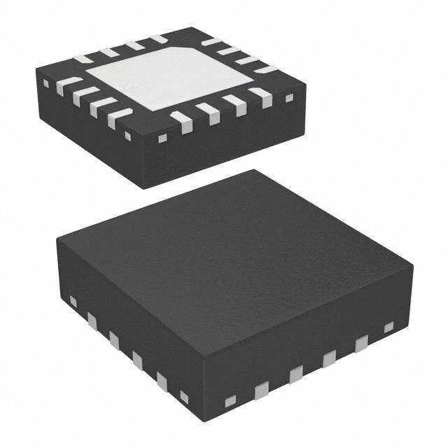
ICGOO在线商城 > 集成电路(IC) > PMIC - LED 驱动器 > TLC5940NTG4
- 型号: TLC5940NTG4
- 制造商: Texas Instruments
- 库位|库存: xxxx|xxxx
- 要求:
| 数量阶梯 | 香港交货 | 国内含税 |
| +xxxx | $xxxx | ¥xxxx |
查看当月历史价格
查看今年历史价格
TLC5940NTG4产品简介:
ICGOO电子元器件商城为您提供TLC5940NTG4由Texas Instruments设计生产,在icgoo商城现货销售,并且可以通过原厂、代理商等渠道进行代购。 TLC5940NTG4价格参考。Texas InstrumentsTLC5940NTG4封装/规格:PMIC - LED 驱动器, LED 驱动器 IC 16 输出 线性 移位寄存器 120mA 28-PDIP。您可以下载TLC5940NTG4参考资料、Datasheet数据手册功能说明书,资料中有TLC5940NTG4 详细功能的应用电路图电压和使用方法及教程。
TLC5940NTG4 是由 Texas Instruments(德州仪器)生产的一款 PMIC - LED 驱动器,广泛应用于需要高精度、多通道电流控制的场景。以下是其主要应用场景:

1. LED 显示屏:TLC5940NTG4 支持 16 通道恒流驱动,每通道可提供高达 120mA 的电流输出,适用于驱动小型 LED 矩阵或显示屏。其 PWM 调光功能支持高达 4096 级灰度调节,能够实现平滑的亮度变化和色彩过渡。

2. RGB 彩灯控制:该芯片适合用于 RGB LED 的驱动与控制,支持通过串行接口(如 SPI 或移位寄存器模式)接收数据,从而精确调整红、绿、蓝三种颜色的亮度,实现丰富的色彩组合。

3. 消费电子设备:例如游戏机、音响设备、家用电器等需要动态指示灯或背光显示的产品中,TLC5940NTG4 可以提供稳定且灵活的 LED 控制方案。

4. 广告牌和标识牌:在户外或室内的 LED 广告牌、标识牌中,这款芯片可以实现复杂的动画效果和亮度调节,适应不同的环境光照条件。

5. 舞台灯光与特效:由于其支持多级灰度调节和快速响应时间,TLC5940NTG4 能够满足舞台灯光对精准亮度控制的需求,创造炫目的视觉效果。

6. 汽车内饰照明:尽管 TLC5940NTG4 更常用于低功率应用,但在某些非关键性车载照明系统中(如氛围灯),它也能发挥作用。

7. 教育与开发平台:由于其易于编程和使用,许多 DIY 项目、教学实验以及开发板中也采用了 TLC5940NTG4 来展示 LED 控制技术。

总之,TLC5940NTG4 凭借其多通道输出、高精度电流源及强大的调光能力,在需要复杂 LED 控制的场合表现出色,为设计师提供了高度灵活性和可靠性。
| 参数 | 数值 |
| 产品目录 | 集成电路 (IC)光电子产品 |
| 描述 | IC LED DRIVER PWM CONTROL 28-DIPLED照明驱动器 4096 Step Grayscale LED Driver |
| 产品分类 | |
| 品牌 | Texas Instruments |
| 产品手册 | |
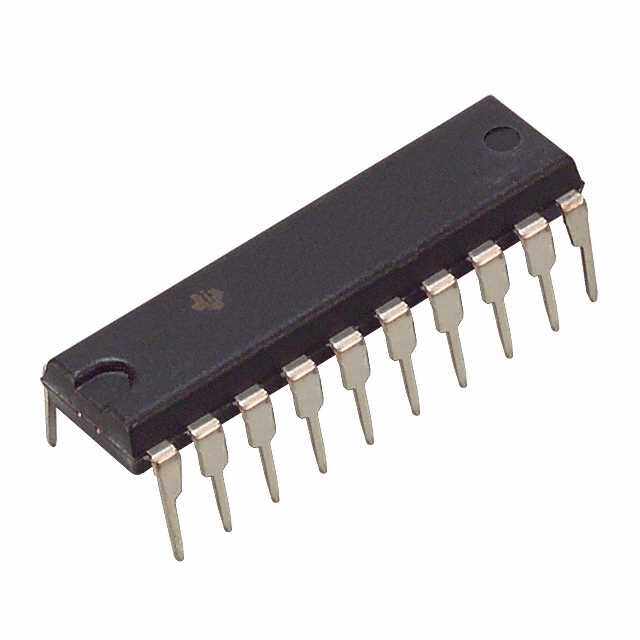
| 产品图片 |
|
| rohs | 符合RoHS无铅 / 符合限制有害物质指令(RoHS)规范要求 |
| 产品系列 | LED照明电子器件,LED照明驱动器,Texas Instruments TLC5940NTG4- |
| 数据手册 | |
| 产品型号 | TLC5940NTG4 |
| 产品种类 | LED照明驱动器 |
| 低电平输出电流 | 1 mA |
| 供应商器件封装 | 28-PDIP |
| 其它名称 | 296-36162-5 |
| 内部驱动器 | 是 |
| 包装 | 管件 |
| 单位重量 | 2.064 g |
| 商标 | Texas Instruments |
| 安装类型 | 通孔 |
| 安装风格 | Through Hole |
| 封装 | Tube |
| 封装/外壳 | 28-DIP(0.300",7.62mm) |
| 封装/箱体 | PDIP-28 |
| 工作温度 | -40°C ~ 85°C |
| 工作频率 | 30 MHz |
| 工厂包装数量 | 13 |
| 恒压 | - |
| 恒流 | 是 |
| 拓扑 | 低端,PWM |
| 拓扑结构 | Boost |
| 最大工作温度 | + 85 C |
| 最大电源电流 | 6 mA |
| 最小工作温度 | - 40 C |
| 标准包装 | 13 |
| 电压-电源 | 3 V ~ 5.5 V |
| 电压-输出 | 17V |
| 类型 | Linear |
| 类型-初级 | 背光 |
| 类型-次级 | - |
| 系列 | TLC5940 |
| 输入电压 | 3 V to 5.5 V |
| 输出数 | 16 |
| 输出电流 | 120 mA |
| 输出端数量 | 16 Output |
| 输出类型 | Constant Current |
| 频率 | 30MHz |
| 高电平输出电流 | - 1 mA |



- 商务部:美国ITC正式对集成电路等产品启动337调查
- 曝三星4nm工艺存在良率问题 高通将骁龙8 Gen1或转产台积电
- 太阳诱电将投资9.5亿元在常州建新厂生产MLCC 预计2023年完工
- 英特尔发布欧洲新工厂建设计划 深化IDM 2.0 战略
- 台积电先进制程称霸业界 有大客户加持明年业绩稳了
- 达到5530亿美元!SIA预计今年全球半导体销售额将创下新高
- 英特尔拟将自动驾驶子公司Mobileye上市 估值或超500亿美元
- 三星加码芯片和SET,合并消费电子和移动部门,撤换高东真等 CEO
- 三星电子宣布重大人事变动 还合并消费电子和移动部门
- 海关总署:前11个月进口集成电路产品价值2.52万亿元 增长14.8%



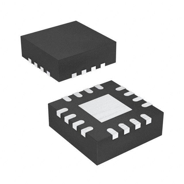
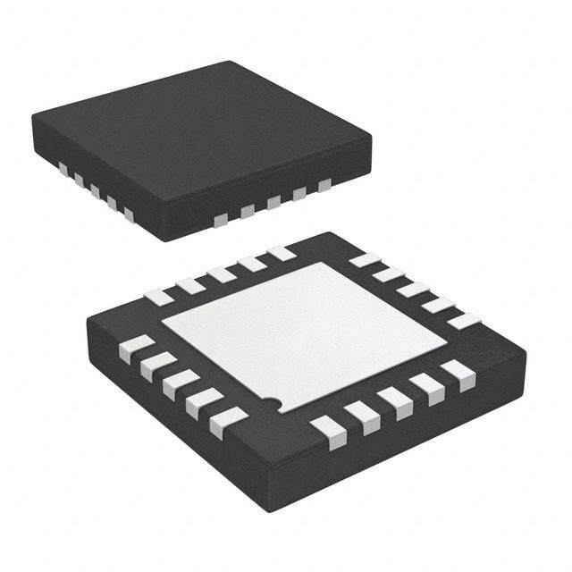

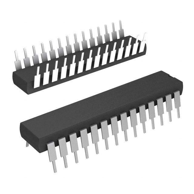
PDF Datasheet 数据手册内容提取
Product Sample & Technical Tools & Support & Folder Buy Documents Software Community TLC5940 SLVS515D–DECEMBER2004–REVISEDNOVEMBER2015 TLC5940 16-Channel LED Driver With DOT Correction and Grayscale PWM Control 1 Features 3 Description • 16Channels The TLC5940 is a 16-channel, constant-current sink 1 LED driver. Each channel has an individually • 12bit(4096Steps)GrayscalePWMControl adjustable 4096-step grayscale PWM brightness • DotCorrection control and a 64-step, constant-current sink (dot – 6bit(64Steps) correction). The dot correction adjusts the brightness variations between LED channels and other LED – StorableinIntegratedEEPROM drivers. The dot correction data is stored in an • DriveCapability(Constant-CurrentSink) integrated EEPROM. Both grayscale control and dot – 0mAto60mA(V < 3.6V) correction are accessible through a serial interface. A CC single external resistor sets the maximum current – 0mAto120mA(V > 3.6V) CC valueofall16channels. • LEDPowerSupplyVoltageupto17V The TLC5940 features two error information circuits. • V =3Vto5.5V CC The LED open detection (LOD) indicates a broken or • SerialDataInterface disconnected LED at an output terminal. The thermal • ControlledIn-RushCurrent error flag (TEF) indicates an overtemperature condition. • 30MHzDataTransferRate • CMOSLevelI/O DeviceInformation(1) • ErrorInformation PARTNUMBER PACKAGE BODYSIZE(NOM) – LOD:LEDOpenDetection PDIP(28) 35.69mm×6.73mm – TEF:ThermalErrorFlag TLC5940 HTSSOP(28) 9.70mm×4.40mm VQFN(32) 5.00mm×5.00mm 2 Applications (1) For all available packages, see the orderable addendum at • Monocolor,Multicolor,Full-ColorLEDDisplays theendofthedatasheet. • LEDSignboards • DisplayBacklighting • General,High-CurrentLEDDrive BlockDiagram VCC GND SCLK SIN XLAT DCPRG CNT VPRG 1 0 Constant Current IREF MCaxu.r rOeUntTn VREF=1.24 V 1 0 VPRG 0 GS Register11 D1CPRG 1P2W−BMit CGornatyrsoclale Dex0laDyriver OUT0 0 DC Register 6−Bit Dot GSCLK 0 5 0 Correction BLANK GS Counter CNT 0DC EEPROM5 LED Open Detection Input VPRG Shift Register CNT Status 0 96 Constant Current InfLoOrmDa,tion: 192 192 12GS Register23 12P−WBMit GCroanytsrocalle Driver OUT1 DCT EDDA,TA 96 D1CPRG Dexl1ay 191 95 96 DC Register 6−Bit Dot 1 0 6 11 0 Correction VPRG 6DC EEPROM11 LED Open Detection LDEeDte Octpioenn 96 VPRG (LOD) Temperature Blank CNT Er(rToEr FFl)ag 1 0 RIeSnghpisiufttter 180GS Register191 12P−WBMit GCroanytsrocalle ConstDanritv eCrurrent OUT15 D1CPRG Dxe1la5y XERR DC Register 6−Bit Dot 90 95 0 Correction 191 90DC EEPROM95 LED Open Detection SOUT VPRG 1 An IMPORTANT NOTICE at the end of this data sheet addresses availability, warranty, changes, use in safety-critical applications, intellectualpropertymattersandotherimportantdisclaimers.PRODUCTIONDATA.
TLC5940 SLVS515D–DECEMBER2004–REVISEDNOVEMBER2015 www.ti.com Table of Contents 1 Features.................................................................. 1 8.2 FunctionalBlockDiagram.......................................13 2 Applications........................................................... 1 8.3 FeatureDescription.................................................13 3 Description............................................................. 1 8.4 DeviceFunctionalModes........................................18 4 RevisionHistory..................................................... 2 9 ApplicationandImplementation........................ 23 9.1 ApplicationInformation............................................23 5 PinConfigurationandFunctions......................... 3 9.2 TypicalApplication .................................................23 6 Specifications......................................................... 5 10 PowerSupplyRecommendations..................... 25 6.1 AbsoluteMaximumRatings......................................5 11 Layout................................................................... 25 6.2 ESDRatings..............................................................5 6.3 RecommendedOperatingConditions.......................5 11.1 LayoutGuidelines.................................................25 6.4 ThermalInformation..................................................6 11.2 LayoutExample....................................................25 6.5 ElectricalCharacteristics...........................................7 11.3 PowerDissipationCalculation..............................26 6.6 SwitchingCharacteristics..........................................8 12 DeviceandDocumentationSupport................. 27 6.7 TypicalCharacteristics..............................................9 12.1 CommunityResources..........................................27 7 ParameterMeasurementInformation................11 12.2 Trademarks...........................................................27 7.1 TestParameterEquations......................................12 12.3 ElectrostaticDischargeCaution............................27 12.4 Glossary................................................................27 8 DetailedDescription............................................ 13 13 Mechanical,Packaging,andOrderable 8.1 Overview.................................................................13 Information........................................................... 27 4 Revision History NOTE:Pagenumbersforpreviousrevisionsmaydifferfrompagenumbersinthecurrentversion. ChangesfromRevisionC(October2007)toRevisionD Page • AddedESDRatingstable,FeatureDescriptionsection,DeviceFunctionalModes,ApplicationandImplementation section,PowerSupplyRecommendationssection,Layoutsection,DeviceandDocumentationSupportsection,and Mechanical,Packaging,andOrderableInformationsection.................................................................................................. 1 ChangesfromRevisionB(September2007)toRevisionC Page • Changedt setuptimefrom:30msto:30ns...................................................................................................................... 6 su5 2 SubmitDocumentationFeedback Copyright©2004–2015,TexasInstrumentsIncorporated ProductFolderLinks:TLC5940
TLC5940 www.ti.com SLVS515D–DECEMBER2004–REVISEDNOVEMBER2015 5 Pin Configuration and Functions PWPPackage 28-PinHTSSOP NTPackage TopView 28-PinPDIP TopView GND 1 28 VCC OUT1 1 28 OUT0 BLANK 2 27 IREF XLAT 3 26 DCPRG OUT2 2 27 VPRG SCLK 4 25 GSCLK OUT3 3 26 SIN SIN 5 24 SOUT OUT4 4 25 SCLK VPRG 6 23 XERR Thermal OUT5 5 24 XLAT OUT0 7 22 OUT15 PAD OUT6 6 23 BLANK OUT1 8 21 OUT14 OUT2 9 20 OUT13 OUT7 7 22 GND OUT3 10 19 OUT12 OUT8 8 21 VCC OUT4 11 18 OUT11 OUT9 9 20 IREF OUT5 12 17 OUT10 OUT10 10 19 DCPRG OUT6 13 16 OUT9 OUT11 11 18 GSCLK OUT7 14 15 OUT8 OUT12 12 17 SOUT OUT13 13 16 XERR OUT14 14 15 OUT15 RHBPackage 32-PinVQFN TopView K 5 4 3 2 1 L T R 1 1 1 1 1 C U R T T T T T S O E U U U U U G S X O O O O O 4 3 2 1 0 9 8 7 2 2 2 2 2 1 1 1 DCPRG 25 16 OUT10 IREF 26 15 OUT9 VCC 27 14 OUT8 NC 28 THERMAL 13 NC NC 29 PAD 12 NC GND 30 11 OUT7 BLANK 31 10 OUT6 XLAT 32 9 OUT5 1 2 3 4 5 6 7 8 K N G 0 1 2 3 4 CL SI PR UT UT UT UT UT S V O O O O O NC–Nointernalconnection Copyright©2004–2015,TexasInstrumentsIncorporated SubmitDocumentationFeedback 3 ProductFolderLinks:TLC5940
TLC5940 SLVS515D–DECEMBER2004–REVISEDNOVEMBER2015 www.ti.com PinFunctions PIN TYPE DESCRIPTION NAME DIPNO. PWPNO. RHBNO. Blankalloutputs.WhenBLANK=H,allOUTnoutputsareforcedOFF. BLANK 23 2 31 I GScounterisalsoreset.WhenBLANK=L,OUTnarecontrolledby grayscalePWMcontrol. SwitchDCdatainput.WhenDCPRG=L,DCisconnectedto EEPROM.WhenDCPRG=H,DCisconnectedtotheDCregister. DCPRG 19 26 25 I DCPRGalsocontrolsEEPROMwriting,whenVPRG=V . (PRG) EEPROMdata=3Fh(default) GND 22 1 30 G Ground GSCLK 18 25 24 I ReferenceclockforgrayscalePWMcontrol IREF 20 27 26 I Referencecurrentterminal — — 12 — — 13 NC — Noconnection — — 28 — — 29 OUT0 28 7 4 O Constantcurrentoutput OUT1 1 8 5 O Constantcurrentoutput OUT2 2 9 6 O Constantcurrentoutput OUT3 3 10 7 O Constantcurrentoutput OUT4 4 11 8 O Constantcurrentoutput OUT5 5 12 9 O Constantcurrentoutput OUT6 6 13 10 O Constantcurrentoutput OUT7 7 14 11 O Constantcurrentoutput OUT8 8 15 14 O Constantcurrentoutput OUT9 9 16 15 O Constantcurrentoutput OUT10 10 17 16 O Constantcurrentoutput OUT11 11 18 17 O Constantcurrentoutput OUT12 12 19 18 O Constantcurrentoutput OUT13 13 20 19 O Constantcurrentoutput OUT14 14 21 20 O Constantcurrentoutput OUT15 15 22 21 O Constantcurrentoutput SCLK 25 4 1 I Serialdatashiftclock SIN 26 5 2 I Serialdatainput SOUT 17 24 23 O Serialdataoutput VCC 21 28 27 I Powersupplyvoltage Multifunctioninputpin.WhenVPRG=GND,thedeviceisinGSmode. WhenVPRG=V ,thedeviceisinDCmode.WhenVPRG=V , VPRG 27 6 3 I CC (VPRG) DCregisterdatacanprogrammedintoDCEEPROMwith DCPRG=HIGH.EEPROMdata=3Fh(default) Erroroutput.XERRisanopen-drainterminal.XERRgoesLwhenLOD XERR 16 23 22 O orTEFisdetected. Leveltriggeredlatchsignal.WhenXLAT=high,theTLC5940writes datafromtheinputshiftregistertoeitherGSregister(VPRG=low)or XLAT 24 3 32 I DCregister(VPRG=high).WhenXLAT=low,thedatainGSorDC registerisheldconstant. 4 SubmitDocumentationFeedback Copyright©2004–2015,TexasInstrumentsIncorporated ProductFolderLinks:TLC5940
TLC5940 www.ti.com SLVS515D–DECEMBER2004–REVISEDNOVEMBER2015 6 Specifications 6.1 Absolute Maximum Ratings overoperatingfree-airtemperaturerange(unlessotherwisenoted)(1) MIN MAX UNIT VCC –0.3 6 V Inputvoltage(2) V ,V ,V ,V ,V , (BLANK) (DCPRG) (SCLK) (XLAT) (SIN) –0.3 V +0.3 V V ,V CC (GSCLK) (IREF) V ,V –0.3 V +0.3 V (SOUT) (XERR) CC Outputvoltage V toV –0.3 18 V (OUT0) (OUT15) Outputcurrent(dc) 130 mA EEPROMprogramrange V –0.3 24 V (VPRG) EEPROMwritecycles 50 — Storagetemperature,T –55 150 °C stg (1) StressesbeyondthoselistedunderAbsoluteMaximumRatingsmaycausepermanentdamagetothedevice.Thesearestressratings only,whichdonotimplyfunctionaloperationofthedeviceattheseoranyotherconditionsbeyondthoseindicatedunderRecommended OpertingConditions.Exposuretoabsolute-maximum-ratedconditionsforextendedperiodsmayaffectdevicereliability. (2) Allvoltagevaluesarewithrespecttonetworkgroundterminal. 6.2 ESD Ratings VALUE UNIT Human-bodymodel(HBM),perANSI/ESDA/JEDECJS-001(1) ±2000 V(ESD) Electrostaticdischarge Charged-devicemodel(CDM),perJEDECspecificationJESD22- ±500 V C101(2) (1) JEDECdocumentJEP155statesthat500-VHBMallowssafemanufacturingwithastandardESDcontrolprocess. (2) JEDECdocumentJEP157statesthat250-VCDMallowssafemanufacturingwithastandardESDcontrolprocess. 6.3 Recommended Operating Conditions MIN NOM MAX UNIT DCCHARACTERISTICS V SupplyVoltage 3 5.5 V CC V Voltageappliedtooutput(OUT0–OUT15) 17 V O V High-levelinputvoltage 0.8V V V IH CC CC V Low-levelinputvoltage GND 0.2V V IL CC I High-leveloutputcurrent V =5VatSOUT –1 mA OH CC I Low-leveloutputcurrent V =5VatSOUT,XERR 1 mA OL CC OUT0toOUT15,V <3.6V 60 mA CC I Constantoutputcurrent OLC OUT0toOUT15,V >3.6V 120 mA CC V EEPROMprogramvoltage 20 22 23 V (VPRG) T Operatingfree-airtemperaturerange -40 85 °C A ACCHARACTERISTICS V =3Vto5.5V,T =–40°Cto85°C(unlessotherwisenoted) CC A f Datashiftclockfrequency SCLK 30 MHz (SCLK) f Grayscaleclockfrequency GSCLK 30 MHz (GSCLK) t /t SCLKpulseduration SCLK=H/L(seeFigure11) 16 ns wh0 wl0 t /t GSCLKpulseduration GSCLK=H/L(seeFigure11) 16 ns wh1 wl1 t XLATpulseduration XLAT=H(seeFigure11) 20 ns wh2 t BLANKpulseduration BLANK=H(seeFigure11) 20 ns wh3 Copyright©2004–2015,TexasInstrumentsIncorporated SubmitDocumentationFeedback 5 ProductFolderLinks:TLC5940
TLC5940 SLVS515D–DECEMBER2004–REVISEDNOVEMBER2015 www.ti.com Recommended Operating Conditions (continued) MIN NOM MAX UNIT t SINtoSCLK↑(1)(seeFigure11) 5 ns su0 t SCLK↓toXLAT↑(seeFigure11) 10 ns su1 t VPRG↑↓toSCLK↑(seeFigure11) 10 ns su2 t Setuptime VPRG↑↓XLAT↑(seeFigure11) 10 ns su3 t BLANK↓toGSCLK↑(seeFigure11) 10 ns su4 t XLAT↑toGSCLK↑(seeFigure11) 30 ns su5 t VPRG↑toDCPRG↑(seeFigure16) 1 ms su6 t SCLK↑toSIN(seeFigure11) 3 ns h0 t XLAT↓toSCLK↑(seeFigure11) 10 ns h1 t SCLK↑toVPRG↑↓(seeFigure11) 10 ns h2 HoldTime t XLAT↓toVPRG↑↓(seeFigure11) 10 ns h3 t GSCLK↑toBLANK↑(seeFigure11) 10 ns h4 t DCPRG↓toVPRG↓(seeFigure11) 1 ms h5 t ProgrammingtimeforEEPROM(seeFigure16) 20 ms prog (1) ↑and↓indicatesarisingedge,andafallingedgerespectively. 6.4 Thermal Information TLC5940 THERMALMETRIC(1) PWP(HTSSOP) RHB(VQFN) UNIT 28PINS 32PINS R Junction-to-ambientthermalresistance 36.7 34.3 °C/W θJA R Junction-to-case(top)thermalresistance 18.9 36.8 °C/W θJC(top) R Junction-to-boardthermalresistance 15.9 8.5 °C/W θJB ψ Junction-to-topcharacterizationparameter 0.6 0.3 °C/W JT ψ Junction-to-boardcharacterizationparameter 15.8 8.7 °C/W JB R Junction-to-case(bottom)thermalresistance 2.3 1.6 °C/W θJC(bot) (1) Formoreinformationabouttraditionalandnewthermalmetrics,seetheSemiconductorandICPackageThermalMetricsapplication report,SPRA953. 6 SubmitDocumentationFeedback Copyright©2004–2015,TexasInstrumentsIncorporated ProductFolderLinks:TLC5940
TLC5940 www.ti.com SLVS515D–DECEMBER2004–REVISEDNOVEMBER2015 6.5 Electrical Characteristics V =3Vto5.5V,T =–40°Cto85°C(unlessotherwisenoted) CC A PARAMETER TESTCONDITIONS MIN TYP MAX UNIT V High-leveloutputvoltage I =-1mA,SOUT V –0.5 V OH OH CC V Low-leveloutputvoltage I =1mA,SOUT 0.5 V OL OL V =V orGND;BLANK,DCPRG,GSCLK,SCLK,SIN, I CC –1 1 XLAT μA II Inputcurrent VI=GND;VPRG –1 1 V =V ;VPRG 50 I CC V =22V;VPRG;DCPRG=V 4 10 mA I CC Nodatatransfer,alloutputOFF, 0.9 6 V =1V,R =10kΩ O (IREF) Nodatatransfer,alloutputOFF, 5.2 12 V =1V,R =1.3kΩ O (IREF) I Supplycurrent mA CC Datatransfer30MHz,alloutputON, 16 25 V =1V,R =1.3kΩ O (IREF) Datatransfer30MHz,alloutputON, 30 60 V =1V,R =640Ω O (IREF) Constantsinkcurrent(see I AlloutputON,V =1V,R =640Ω 54 61 69 mA O(LC) Figure10) O (IREF) AlloutputOFF,V =15V,R =640Ω, I Leakageoutputcurrent O (IREF) 0.1 μA lkg OUT0toOUT15 AlloutputON,V =1V,R =640Ω, O (IREF) ±1% ±4% OUT0toOUT15,–20°Cto85°C AlloutputON,V =1V,R =640Ω, O (IREF) ±1% ±8% Constantsinkcurrenterror OUT0toOUT15(1) ΔI O(LC0) (seeFigure10) AlloutputON,V =1V,R =320Ω, O (IREF) ±1% ±6% OUT0toOUT15,–20°Cto85°C AlloutputON,V =1V,R =320Ω, O (IREF) ±1% ±8% V =4.5Vto5.5V,OUT0toOUT15(1) CC Constantsinkcurrenterror Devicetodevice,AveragedcurrentfromOUT0to –2% ΔIO(LC1) (seeFigure10) OUT15,R(IREF)=1920Ω(20mA)(2) +0.4% ±4% Constantsinkcurrenterror Devicetodevice,AveragedcurrentfromOUT0to –2.7% ΔIO(LC2) (seeFigure10) OUT15,R(IREF)=480Ω(80mA)(2) +2% ±4% AlloutputON,V =1V,R =640Ω O (IREF) ±1 ±4 %/V OUT0toOUT15,V =3Vto5.5V(3) ΔI Lineregulation(seeFigure10) CC O(LC3) AlloutputON,V =1V,R =320Ω, OUT0toOUT15O,V =3(VIREtoF)5.5V(3) ±1 ±6 %/V CC AlloutputON,V =1Vto3V,R =640Ω, O (IREF) ±2 ±6 %/V Loadregulation(see OUT0toOUT15(4) ΔI O(LC4) Figure10) AlloutputON,V =1Vto3V,R =320Ω, OUT0toOUT15O(4) (IREF) ±2 ±8 %/V T Thermalerrorflagthreshold Junctiontemperature(5) 150 170 °C (TEF) V LEDopendetectionthreshold 0.3 0.4 V (LED) Referencevoltage V R =640Ω 1.20 1.24 1.28 V (IREF) output (IREF) (1) ThedeviationofeachoutputfromtheaverageofOUT0-15constantcurrent.ItiscalculatedbyEquation1inTestParameterEquations. (2) ThedeviationofaverageofOUT1-15constantcurrentfromtheidealconstant-currentvalue.ItiscalculatedbyEquation2inTest ParameterEquations.TheidealcurrentiscalculatedbyEquation3inTestParameterEquations. (3) ThelineregulationiscalculatedbyEquation4inTestParameterEquations. (4) TheloadregulationiscalculatedbyEquation5inTestParameterEquations. (5) Nottested.Specifiedbydesign Copyright©2004–2015,TexasInstrumentsIncorporated SubmitDocumentationFeedback 7 ProductFolderLinks:TLC5940
TLC5940 SLVS515D–DECEMBER2004–REVISEDNOVEMBER2015 www.ti.com 6.6 Switching Characteristics V =3Vto5.5V,T =-40°Cto85°C(unlessotherwisenoted) CC A PARAMETER TESTCONDITIONS MIN TYP MAX UNIT t SOUT 16 r0 Risetime ns t OUTn,V =5V,T =60°C,DCn=3Fh 10 30 r1 CC A t SOUT 16 f0 Falltime ns t OUTn,V =5V,T =60°C,DCn=3Fh 10 30 f1 CC A t SCLKtoSOUT(seeFigure11) 30 ns pd0 t BLANKtoOUT0 60 ns pd1 t OUTntoXERR(seeFigure11) 1000 ns pd2 Propagationdelaytime t GSCLKtoOUT0(seeFigure11) 60 ns pd3 t XLATtoI (dotcorrection)(seeFigure11) 60 ns pd4 OUT t DCPRGtoOUT0(seeFigure11) 30 ns pd5 t Outputdelaytime OUTntoOUT(n+1)(seeFigure11) 20 30 ns d t Outputon-timeerror t –T (seeFigure11),GSn=01h,GSCLK=11MHz 10 –50 –90 ns on-err outon gsclk 8 SubmitDocumentationFeedback Copyright©2004–2015,TexasInstrumentsIncorporated ProductFolderLinks:TLC5940
TLC5940 www.ti.com SLVS515D–DECEMBER2004–REVISEDNOVEMBER2015 6.7 Typical Characteristics 10 k 4 k TLC5940PWP 7.68 kΩ PowerPAD Soldered W W TLC5940RHB -REF) e - m 3 k Resistor, R(I 1 k 1.92 kΩ 0.96 kΩ sipation Rat 2 k TLC5940NT ce 0.64 kΩ Dis eren 0.48 kΩ 0.38 kΩ wer TPLoCw5e9rP4A0PDW UPnsoldered Ref 0.32 kΩ Po 1 k 100 0 0 20 40 60 80 100 120 -40 -20 0 20 40 60 80 100 IO−Output Current−mA TA−Free-Air Temperature−oC Figure1.ReferenceResistorvsOutputCurrent Figure2.PowerDissipationRatevsFree-AirTemperature 140 65 120 TVACC= =2 55° CV, IO= 120 mA 64 IVOC=C 6=0 5 m VA, TA= 85°C IO= 100 mA 63 mA 100 mA 62 urrent - 80 IO= 80 mA urrent - 61 utput C 60 IO= 60 mA utput C 5690 TA= -40°C TA= 25°C I- OO 40 IO= 40 mA I- OO 58 IO= 20 mA 57 20 IO= 5 mA 56 0 55 0 0.5 1 1.5 2 2.5 3 0 0.5 1 1.5 2 2.5 3 VO- Output Voltage - V VO- Output Voltage - V Figure3.OutputCurrentvsOutputVoltage Figure4.OutputCurrentvsOutputVoltage 8 8 IO= 60 mA TA= 25°C, % 6 % 6 VCC= 5 V Output Current - 024 VCC= 3.3 V Output Current - 024 ΔI- Constant OLC---642 VCC= 5 V ΔI- Constant OLC---642 -8 -8 -40 -20 0 20 40 60 80 100 0 20 40 60 80 TA-Ambient Temperature -°C IO- Output Current - mA Figure5.ConstantOutputCurrent,ΔIOLC Figure6.ConstantOutputCurrent,ΔIOLC vsAmbientTemperature vsOutputCurrent Copyright©2004–2015,TexasInstrumentsIncorporated SubmitDocumentationFeedback 9 ProductFolderLinks:TLC5940
TLC5940 SLVS515D–DECEMBER2004–REVISEDNOVEMBER2015 www.ti.com Typical Characteristics (continued) 140 70 120 TVACC= =2 55° CV, IO= 120 mA 60 IVOC=C 6=0 5 m VA, TA= 25°C mA 100 mA 50 TA= 85°C Current - 80 IO= 80 mA Current - 40 TA= -40°C Output 60 IO= 60 mA Output 30 I- O 40 IO= 30 mA I- O20 20 10 IO= 5 mA 0 0 0 10 20 30 40 50 60 70 0 10 20 30 40 50 60 70 Dot Correction Data - dec Dot Correction Data - dec Figure7.OutputCurrent Figure8.OutputCurrent vsDOTCorrectionLinearity(ABSValue) vsDOTCorrectionLinearity(ABSValue) 10 SubmitDocumentationFeedback Copyright©2004–2015,TexasInstrumentsIncorporated ProductFolderLinks:TLC5940
TLC5940 www.ti.com SLVS515D–DECEMBER2004–REVISEDNOVEMBER2015 7 Parameter Measurement Information Resistorvaluesareequivalentresistances,andtheyarenottested. INPUT EQUIVALENT CIRCUIT OUTPUT EQUIVALENT CIRCUIT (SOUT) (BLANK, XLAT, SCLK, SIN, GSCLK, DCPRG) VCC VCC 400W 23W INPUT SOUT 23W GND GND INPUT EQUIVALENT CIRCUIT (IREF) OUTPUT EQUIVALENT CIRCUIT (XERR) V VCC (IREF) 23W Amp XERR _ 400W + INPUT 100W GND GND INPUT EQUIVALENT CIRCUIT (VCC) OUTPUT EQUIVALENT CIRCUIT (OUT) INPUT OUT GND INPUT EQUIVALENT CIRCUIT (VPRG) INPUT GND GND Figure9. InputandOutputEquivalentCircuits Copyright©2004–2015,TexasInstrumentsIncorporated SubmitDocumentationFeedback 11 ProductFolderLinks:TLC5940
TLC5940 SLVS515D–DECEMBER2004–REVISEDNOVEMBER2015 www.ti.com Parameter Measurement Information (continued) t , t , t t , t , t , t , t , t , t , t r0 f0 pd0 r1 f1 pd1 pd2 pd3 pd4 pd5 d V = 4V O SOUT Testpoint R = 51W C = 15pF L L OUTn Testpoint C = 15pF L I ,DI ,DI ,DI ,DI DI O(LC) O(LC0) O(LC1) O(LC2) O(LC3) O(LC4) OUTn OUTn V = 1V O V = 1V to 3V O V t (IREF) pd3 IREF Testpoint VCC R(IREG)= 640W 470kΩ XERR Figure10. ParameterMeasurementCircuits 7.1 Test Parameter Equations I -I D(%)= OUTn OUTavg_0-15 ´100 I OUTavg_0-15 (1) I -I D(%)= OUTavg OUT(IDEAL) ´100 I OUT(IDEAL) (2) æ1.24Vö IOUT(IDEAL) =31.5´çç ÷÷ èR ø IREF (3) (I atV = 5.5V)-(I atV =3.0V) 100 D(%/V)= OUTn CC OUTn CC ´ (I atV =3.0V) 2.5 OUTn CC (4) (I atV =3.0V)-(I atV =1.0V) 100 D(%/V)= OUTn OUTn OUTn OUTn ´ (I atV =1.0V) 2.0 OUTn OUTn (5) 12 SubmitDocumentationFeedback Copyright©2004–2015,TexasInstrumentsIncorporated ProductFolderLinks:TLC5940
TLC5940 www.ti.com SLVS515D–DECEMBER2004–REVISEDNOVEMBER2015 8 Detailed Description 8.1 Overview The TLC5940 is a 16-channel constant current sink driver. Each channel has an individually-adjustable, 4096- step, pulse width modulation (PWM), grayscale (GS) brightness control, and a 64-step dot correction brightness control. GS data and DC data are input via a serial interface port. The dot correction data is stored in an integrated EEPROM. The TLC5940 has a 120-mA current capability. The maximum current value of all channels is determined by an external resistor. The TLC5940 has a LED open detection (LOD) function that indicates a broken or disconnected LED at an output terminal and a thermal error flag (TEF) indicates an overtemperature condition. 8.2 Functional Block Diagram VCC GND SCLK SIN XLAT DCPRG CNT VPRG 1 0 Constant Current IREF MCaxu.r rOeUntTn VREF=1.24 V 1 0 VPRG 0 GS Register11 D1CPRG 1P2W−BMit CGornatyrsoclale Dex0laDyriver OUT0 0 DC Register 6−Bit Dot 0 5 0 Correction GSCLK BLANK GS Counter CNT 0 DC EEPROM5 LED Open Detection Input VPRG Shift Register CNT Status 0 96 Constant Current Information: 192 192 GS Register 12−Bit Grayscale Driver OUT1 LOD, 12 23 PWM Control DCT EDDA,TA 96 D1CPRG Dexl1ay 191 95 96 DC Register 6−Bit Dot 1 0 6 11 0 Correction VPRG 6DC EEPROM11 LED Open Detection LDEeDte Octpioenn 96 VPRG (LOD) Temperature Blank CNT Error Flag (TEF) 1 0 Input Constant Current Shift GS Register 12−Bit Grayscale Driver OUT15 Register 180 191 PWM Control DCPRG Dxe1la5y 1 XERR DC Register 6−Bit Dot 90 95 0 Correction 191 90DC EEPROM95 LED Open Detection SOUT VPRG 8.3 Feature Description 8.3.1 SerialInterface The TLC5940 has a flexible serial interface, which can be connected to microcontrollers or digital signal processors in various ways. Only 3 pins are needed to input data into the device. The rising edge of SCLK signal shifts the data from the SIN pin to the internal register. After all data is clocked in, a high-level pulse of XLAT signal latches the serial data to the internal registers. The internal registers are level-triggered latches of XLAT signal. All data are clocked in with the MSB first. The length of serial data is 96 bit or 192 bit, depending on the programming mode. Grayscale data and dot correction data can be entered during a grayscale cycle. Although new grayscale data can be clocked in during a grayscale cycle, the XLAT signal should only latch the grayscale data at the end of the grayscale cycle. Latching in new grayscale data immediately overwrites the existing grayscale data. Figure 11 shows the timing chart. More than two TLC5940s can be connected in series by connecting an SOUT pin from one device to the SIN pin of the next device. An example of cascading two TLC5940s is shown in Figure 12 and the timing chart is shown in Figure 13. The SOUT pin can also be connectedtothecontrollertoreceivestatusinformationfromTLC5940asshowninFigure22. Copyright©2004–2015,TexasInstrumentsIncorporated SubmitDocumentationFeedback 13 ProductFolderLinks:TLC5940
TLC5940 SLVS515D–DECEMBER2004–REVISEDNOVEMBER2015 www.ti.com Feature Description (continued) VPRG DC Data Input Mode GS Data Input Mode th3 tsu3 twh2 XLAT 1st GS Data Input Cycle 2nd GS Data Input Cycle SIN MDSCB LDSCB MGSSB1 GLSSB1 MGSSB2 LGSSB2 MGSSB3 th2 tsu2 tsu1 th1 twh0 tsu0 th0 SCLK 1 96 1 192 193 1 192 193 1 twl0 tpd0 SOUT - MDSCB - - MGSSB1 SMISDB1MSSIBD-11 SLISDB1 MGSSB2 SMISDB2 MSSIDB2-1 twh3 BLANK 1st GS Data Output Cycle 2nd GS Data Output Cycle tsu5 th4 tsu4 twh1 GSCLK 1 4096 1 tpd4 tpd1 tpd3 tpd3 Tgsclk twl1 OUT0 (current) tpd1+ td td tpd3+ td touton OUT1 (current) tpd1+ 15 x td 15 x td OUT15 (current) tpd2 XERR Figure11. SerialDataInputTimingChart SIN(a) SIN SOUT SIN SOUT SOUT(b) TLC5940 (a) TLC5940 (b) SCLK, XLAT, BLANK, GSCLK, DCPRG, VPRG Figure12. CascadingTwoTLC5940Devices 14 SubmitDocumentationFeedback Copyright©2004–2015,TexasInstrumentsIncorporated ProductFolderLinks:TLC5940
TLC5940 www.ti.com SLVS515D–DECEMBER2004–REVISEDNOVEMBER2015 Feature Description (continued) VPRG XLAT DCb DCa GSb1 GSa1 GSb2 GSa2 GSb3 SIN(a) MSB LSB MSB LSB MSB LSB MSB SCLK 1 192 1 384 385 1 384 385 1 96X2 192X2 SOUT(b) - MDSCBb - - GMSSbB1 SMIDSbB1 MSSIDBb-11 SLISDBa1 GMSSbB2 SMIDSbB2MSISDBb-12 BLANK GSCLK 1 4096 1 OUT0 (current) OUT1 (current) OUT15 (current) XERR Figure13. TimingChartforTwoCascadedTLC5940Devices 8.3.2 ErrorInformationOutput The open-drain output XERR is used to report both of the TLC5940 error flags, TEF and LOD. During normal operating conditions, the internal transistor connected to the XERR pin is turned off. The voltage on XERR is pulled up to V through an external pullup resistor. If TEF or LOD is detected, the internal transistor is turned CC on, and XERR is pulled to GND. Since XERR is an open-drain output, multiple ICs can be OR'ed together and pulleduptoV withasinglepullupresistor.Thisreducesthenumberofsignalsneededtoreportasystemerror CC (seeFigure22). TodifferentiateLODandTEFsignalfromXERRpin,LODcanbemaskedoutwithBLANK=HIGH. Table1.XERRTruthTable ERRORCONDITION ERRORINFORMATION SIGNALS TEMPERATURE OUTnVOLTAGE TEF LOD BLANK XERR T <T Don'tCare L X H J (TEF) H T >T Don'tCare H X L J (TEF) OUTn>V L L H (LED) T <T J (TEF) OUTn<V L H L (LED) L OUTn>V H L L (LED) T >T J (TEF) OUTn<V H H L (LED) Copyright©2004–2015,TexasInstrumentsIncorporated SubmitDocumentationFeedback 15 ProductFolderLinks:TLC5940
TLC5940 SLVS515D–DECEMBER2004–REVISEDNOVEMBER2015 www.ti.com 8.3.3 TEF:ThermalErrorFlag TheTLC5940providesatemperatureerrorflag(TEF)circuittoindicateanovertemperatureconditionoftheIC.If the junction temperature exceeds the threshold temperature (160°C typical), TEF becomes H and XERR pin goes to low level. When the junction temperature becomes lower than the threshold temperature, TEF becomes LandXERRpinbecomeshighimpedance.TEFstatuscanalsobereadoutfromtheTLC5940statusregister. 8.3.4 LOD:LEDOpenDetection The TLC5940 has an LED-open detector that detects broken or disconnected LEDs. The LED open detector pulls the XERR pin to GND when an open LED is detected. XERR and the corresponding error bit in the Status InformationDataisonlyactiveunderthefollowingopen-LEDconditions. 1. OUTnisonandthetimetpd2(1μstypical)haspassed. 2. ThevoltageofOUTnis <0.3V(typical) The LOD status of each output can be also read out from the SOUT pin. See STATUS INFORMATION OUTPUT section for details. The LOD error bits are latched into the Status Information Data when XLAT returns to a low after a high. Therefore, the XLAT pin must be pulsed high then low while XERR is active in order to latch the LODerrorintotheStatusInformationDataforsubsequentreadingviatheserialshiftregister. 8.3.5 DelayBetweenOutputs The TLC5940 has graduated delay circuits between outputs. These circuits can be found in the constant current driverblockofthedevice(seethefunctionalblockdiagram).Thefixed-delaytimeis20ns(typical),OUT0hasno delay, OUT1 has a 20-ns delay, and OUT2 has a 40-ns delay, etc. The maximum delay is 300 ns from OUT0 to OUT15. The delay works during switch on and switch off of each output channel. These delays prevent large inrushcurrentswhichreducesthebypasscapacitorswhentheoutputsturnon. 8.3.6 OutputEnable All OUTn channels of the TLC5940 can be switched off with one signal. When BLANK is set high, all OUTn channels are disabled, regardless of logic operations of the device. The grayscale counter is also reset. When BLANK is set low, all OUTn channels work under normal conditions. If BLANK goes low and then back high again in less than 300 ns, all outputs programmed to turn on still turn on for either the programmed number of grayscale clocks, or the length of time that the BLANK signal was low, which ever is lower. For example, if all outputs are programmed to turn on for 1 ms, but the BLANK signal is only low for 200 ns, all outputs still turn on for200ns,eventhoughsomeoutputsareturningonaftertheBLANKsignalhasalreadygonehigh. Table2.BLANKSignalTruthTable BLANK OUT0-OUT15 LOW Normalcondition HIGH Disabled 16 SubmitDocumentationFeedback Copyright©2004–2015,TexasInstrumentsIncorporated ProductFolderLinks:TLC5940
TLC5940 www.ti.com SLVS515D–DECEMBER2004–REVISEDNOVEMBER2015 8.3.7 SettingMaximumChannelCurrent The maximum output current per channel is programmed by a single resistor, R , which is placed between (IREF) IREF pin and GND pin. The voltage on IREF is set by an internal band gap V with a typical value of (IREF) 1.24 V. The maximum channel current is equivalent to the current flowing through R multiplied by a factor of (IREF) 31.5.ThemaximumoutputcurrentperchannelcanbecalculatedbyEquation6. V (IREF) Imax = × 31.5 R (IREF) where • V =1.24V (IREF) • R =User-selectedexternalresistor. (6) (IREF) I must be set between 5 mA and 120 mA. The output current may be unstable if I is set lower than 5 mA. max max Output currents lower than 5 mA can be achieved by setting Imax to 5 mA or higher and then using dot correction. Figure 1 shows the maximum output current I versus R . R is the value of the resistor between IREF O (IREF) (IREF) terminal to GND, and I is the constant output current of OUT0 to OUT15. A variable power supply may be O connected to the IREF pin through a resistor to change the maximum output current per channel. The maximum outputcurrentperchannelis31.5timesthecurrentflowingoutoftheIREFpin. Copyright©2004–2015,TexasInstrumentsIncorporated SubmitDocumentationFeedback 17 ProductFolderLinks:TLC5940
TLC5940 SLVS515D–DECEMBER2004–REVISEDNOVEMBER2015 www.ti.com 8.4 Device Functional Modes 8.4.1 OperatingModes The TLC5940 has operating modes depending on the signals DCPRG and VPRG. Table 3 shows the available operating modes. The TPS5940 GS operating mode (see Figure 11) and shift register values are not defined after power up. One solution to solve this is to set dot correction data after TLS5940 power-up and switch back to GS PWM mode. The other solution is to overflow the input shift register with 193 bits of dummy data and latch it while TLS540 is in GS PWM mode. The values in the input shift register, DC register and GS register are unknown just after power on. The DC and GS register values should be properly stored through the serial interfacebeforestartingtheoperation. Table3.TLC5940OperatingModesTruthTable SIGNAL INPUTSHIFTREGISTER MODE DCVALUE DCPRG VPRG L EEPROM GND 192bit GrayscalePWMMode H DCRegister L EEPROM V 96bit DotCorrectionDataInputMode CC H DCRegister L EEPROM H V(VPRG) X EEPROMProgrammingMode WritedcregistervaluetoEEPROM.(Default data:3Fh) 8.4.2 SettingDOTCorrection TheTLC5940hasthecapabilitytofineadjusttheoutputcurrentofeachchannelOUT0toOUT15independently. This is also called dot correction. This feature is used to adjust the brightness deviations of LEDs connected to the output channels OUT0 to OUT15. Each of the 16 channels can be programmed with a 6-bit word. The channel output can be adjusted in 64 steps from 0% to 100% of the maximum output current I . Dot correction max forallchannelsmustbeenteredatthesametime.Equation7 determinestheoutputcurrentforeachoutputn. DCn IOUTn = Imax × 63 where • I =themaximumprogrammableoutputcurrentforeachoutput. max • DCn=theprogrammeddotcorrectionvalueforoutputn(DCn=0to63). • n=0to15 (7) Figure 14 shows the dot correction data packet format which consists of 6 bits x 16 channel, total 96 bits. The format is Big-Endian format. This means that the MSB is transmitted first, followed by the MSB-1, etc. The DC 15.5inFigure14standsforthe5thmostsignificantbitforoutput15. MSB LSB 95 90 89 6 5 0 DC 15.5 DC 15.0 DC 14.5 DC 1.0 DC 0.5 DC 0.0 DC OUT15 DC OUT14−DC OUT2 DC OUT0 Figure14. DotCorrectionDataPacketFormat When VPRG is set to VCC, the TLC5940 enters the dot correction data input mode. The length of input shift register becomes 96 bits. After all serial data are shifted in, the TLC5940 writes the data in the input shift register to DC register when XLAT is high, and holds the data in the DC register when XLAT is low. The DC register is a level triggered latch of XLAT signal. Since XLAT is a level-triggered signal, SCLK and SIN must not be changed while XLAT is high. After XLAT goes low, data in the DC register is latched and does not change. BLANK signal doesnotneedtobehightolatchinnewdata.XLAThassetuptime(tsu1)andholdtime(th1)toSCLKasshown inFigure15. 18 SubmitDocumentationFeedback Copyright©2004–2015,TexasInstrumentsIncorporated ProductFolderLinks:TLC5940
TLC5940 www.ti.com SLVS515D–DECEMBER2004–REVISEDNOVEMBER2015 DC Mode Data DC Mode Data Input Cycle n VCC Input Cycle n+1 VPRG DC n−1 DC n DC n DC n DC n DC n DC n+1 DC n+1 SIN LSB MSB MSB−1 MSB−2 LSB+1 LSB MSB MSB−1 twh0 SCLK 1 2 3 95 96 1 2 twl0 DC n−1 DC n−1 DC n−1 DC n−1 DC n−1 DC n DC n DC n SOUT MSB MSB−1 MSB−2 LSB+1 LSB MSB MSB−1 MSB−2 tsu1 twh2 th1 XLAT Figure15. DotCorrectionDataInputTimingChart The TLC5940 also has an EEPROM to store dot correction data. To store data from the dot correction register to EEPROM, DCPRG is set to high after applying V to the VPRG pin. Figure 16 shows the EEPROM PRG programmingtimings.TheEEPROMhasadefaultvalueofall1s. V(PRG) VPRG VCC tsu6 tprog th5 DCPRG XLAT SIN DC DC MSB LSB SCLK 1 96 SOUT - MDSCB Figure16. EEPROMProgrammingTimingChart DCPRG t t pd5 pd5 OUT0 (Current) OUT15 (Current) Figure17. DCPRGandOUTnTimingDiagram Copyright©2004–2015,TexasInstrumentsIncorporated SubmitDocumentationFeedback 19 ProductFolderLinks:TLC5940
TLC5940 SLVS515D–DECEMBER2004–REVISEDNOVEMBER2015 www.ti.com 8.4.3 SettingGrayscale The TLC5940 can adjust the brightness of each channel OUTn using a PWM control scheme. The use of 12 bits per channel results in 4096 different brightness steps, respective 0% to 100% brightness. Equation 8 determines thebrightnesslevelforeachoutputn. GSn Brightnessin% = × 100 4095 where • GSn=theprogrammedgrayscalevalueforoutputn(GSn=0to4095) • n=0to15 • GrayscaledataforallOUTn (8) Figure 18 shows the grayscale data packet format which consists of 12 bits x 16 channels, totaling 192 bits. The formatisBig-Endianformat.ThismeansthattheMSBistransmittedfirst,followedbytheMSB-1,etc. MSB LSB 191 180 179 12 11 0 GS 15.11 GS 15.0 GS 14.11 GS 1.0 GS 0.11 GS 0.0 GS OUT15 GS OUT14−GS OUT2 GS OUT0 Figure18. GrayscaleDataPacketFormat When VPRG is set to GND, the TLC5940 enters the grayscale data input mode. The device switches the input shift register to 192-bit width. After all data is clocked in, a rising edge of the XLAT signal latches the data into the grayscale register (see Figure 11). New grayscale data immediately becomes valid at the rising edge of the XLAT signal; therefore, new grayscale data should be latched at the end of a grayscale cycle when BLANK is high.The first GS data input cycle after dot correction requires an additional SCLK pulse after the XLAT signal to complete the grayscale update cycle. All GS data in the input shift register is replaced with status information data(SID)afterupdatedthegrayscaleregister. 8.4.4 StatusInformationOutput The TLC5940 does have a status information register, which can be accessed in grayscale mode (VPRG=GND). AftertheXLATsignallatchesthedataintotheGSregistertheinputshiftregisterdatawillbereplacedwithstatus information data (SID) of the device (see Figure 18). LOD, TEF, and dot correction EEPROM data (DCPRG=LOW) or dot correction register data (DCPRG=HIGH) can be read out at SOUT pin. The status information data packet is 192 bits wide. Bits 0-15 contain the LOD status of each channel. Bit 16 contains the TEF status. If DCPRG is low, bits 24-119 contain the data of the dot-correction EEPROM. If DCPRG is high, bits 24-119 contain the data of the dot-correction register.The remaining bits are reserved. The complete status informationdatapacketisshowninFigure19. SOUT outputs the MSB of the SID at the same time the SID are stored in the SID register, as shown Figure 20. The next SCLK pulse, which will be the clock for receiving the SMB of the next grayscale data, transmits MSB-1 of SID. If output voltage is < 0.3 V (typical) when the output sink current turns on, LOD status flage becomes active. The LOD status flag is an internal signal that pulls XERR pin down to low when the LOD status flag becomes active. The delay time, tpd2 (1 μs maximum), is from the time of turning on the output sink current to the time LOD status flage becomes valid. The timing for each channel's LOD status to become valid is shifted by the 30-ns (maximum) channel-to-channel turn-on time. After the first GSCLK goes high, OUT0 LOD status is valid; tpd3 + tpd2 = 60 ns + 1 μs. OUT1 LOD status is valid; tpd3 + td + tpd2 = 60 ns + 30 ns + 1 μs = 1.09 μs. OUT2 LOD status is valid; tpd3 + 2*td + tpd2 = 1.12 μs, and so on. It takes 1.51 μs maximum (tpd3 + 15*td + tpd2) from the first GSCLK rising edge until all LOD become valid; tsuLOD must be > 1.51 μs (see Figure 20) to ensurethatallLODdataarevalid. 20 SubmitDocumentationFeedback Copyright©2004–2015,TexasInstrumentsIncorporated ProductFolderLinks:TLC5940
TLC5940 www.ti.com SLVS515D–DECEMBER2004–REVISEDNOVEMBER2015 MSB LSB 0 15 16 23 24 119 120 191 LOD 15 LOD 0 TEF X X DC 15.5 DC 0.0 X X LOD Data TEF DC Values Reserved Figure19. StatusInformationDataPacketFormat VPRG GS Data Input Mode XLAT 1st GS Data Input Cycle 2nd GS Data Input Cycle SIN GS1 GS1 GS2 GS2 MSB LSB MSB LSB > tpd4 + 15 x td + tpd3 tsuLOD SCLK 1 192 193 1 192 SOUT - - MGSSB1 SMISDB1 MSSIDB-11 SLISDB1 MGSSB2 BLANK (1st GS Data Output Cycle) GSCLK 1 4096 tpd3 OUT0 (current) td OUT1 (current) 15 x td OUT15 (current) tpd2 XERR tpd3+ 15 x td+ tpd2 Figure20. ReadoutStatusInformationData(SID)TimingChart 8.4.5 GrayscalePWMOperation The grayscale PWM cycle starts with the falling edge of BLANK. The first GSCLK pulse after BLANK goes low increases the grayscale counter by one and switches on all OUTn with grayscale value not zero. Each following rising edge of GSCLK increases the grayscale counter by one. The TLC5940 compares the grayscale value of each output OUTn with the grayscale counter value. All OUTn with grayscale values equal to the counter values are switched off. A BLANK=H signal after 4096 GSCLK pulses resets the grayscale counter to zero and completes the grayscale PWM cycle (see Figure 21). When the counter reaches a count of FFFh, the counter stops counting and all outputs turn off. Pulling BLANK high before the counter reaches FFFh immediately resets thecountertozero. Copyright©2004–2015,TexasInstrumentsIncorporated SubmitDocumentationFeedback 21 ProductFolderLinks:TLC5940
TLC5940 SLVS515D–DECEMBER2004–REVISEDNOVEMBER2015 www.ti.com GS PWM GS PWM Cycle n Cycle n+1 BLANK twh1 twl1 th4 twh3 tsu4 GSCLK 1 2 3 4096 1 twl1 tpd1 tpd3 tpd3 OUT0 (Current) OUT1 tpd1+ td n x t d tpd3+ n x td (Current) tpd1+ 15 x td OUT15 (Current) tpd2 XERR Figure21. GrayscalePWMCycleTimingChart 22 SubmitDocumentationFeedback Copyright©2004–2015,TexasInstrumentsIncorporated ProductFolderLinks:TLC5940
TLC5940 www.ti.com SLVS515D–DECEMBER2004–REVISEDNOVEMBER2015 9 Application and Implementation NOTE Information in the following applications sections is not part of the TI component specification, and TI does not warrant its accuracy or completeness. TI’s customers are responsible for determining suitability of components for their purposes. Customers should validateandtesttheirdesignimplementationtoconfirmsystemfunctionality. 9.1 Application Information The device is a 16-channel, constant sink current, LED driver. This device can be connected in series to drive many LED lamps with only a few controller ports. Output current control data, dot correction data and PWM controldatacanbewrittenfromtheSINinputterminal. 9.2 Typical Application VCC V(LED) V(LED) V(LED) V(LED) 100 k OUT0 OUT15 OUT0 OUT15 SIN SIN SOUT SIN SOUT XERR XERR VCC XERR VCC SCLK SCLK SCLK XLAT XLAT 100 nF XLAT 100 nF GSCLK GSCLK TLC5940 GSCLK TLC5940 Controller DCPRG DCPRG IREF DCPRG IREF BLANK BLANK BLANK SOUT VPRG IC 0 VPRG IC n W_EEPROM VPRG_D 7 VPRG_OE V(22V) V(22V) 50 k 50 k 50 k 50 k 50 k 50 k VPRG Figure22. CascadingDevices 9.2.1 DesignRequirements Forthisdesignexample,usetheinputparametersshowninTable4. Table4.DesignParameters PARAMETERS VALUES VCCinputvoltagerange 3.0Vto5.5V LEDlamp(V )inputvoltagerange >MaximumLEDforwardvoltage(V )+ICkneevoltage LED F SIN,SCLK,XLAT,GSCLK,andBLANKvoltagerange Lowlevel=GND,Highlevel=VCC Copyright©2004–2015,TexasInstrumentsIncorporated SubmitDocumentationFeedback 23 ProductFolderLinks:TLC5940
TLC5940 SLVS515D–DECEMBER2004–REVISEDNOVEMBER2015 www.ti.com 9.2.2 DetailedDesignProcedure 9.2.2.1 SerialDataTransferRate Figure 22 shows a cascading connection of n TLC5940 devices connected to a controller, building a basic module of an LED display system. The maximum number of cascading TLC5940 devices depends on the applicationsystemandisintherangeof40devices.Equation9calculatestheminimumfrequencyneeded: f = 4096 × f (GSCLK) (update) f = 193 × f × n (SCLK) (update) where • f :minimumfrequencyneededforGSCLK (GSCLK) • f :minimumfrequencyneededforSCLKandSIN (SCLK) • f :updaterateofwholecascadingsystem (update) • n:numbercascadedofTLC5940device (9) 9.2.2.2 Grayscale(GS)Data There are a total of 16 sets of 12-bit GS data for the PWM control of each output. Select the GS data of each LEDlampandwritetheGSdatatotheregisterfollowingthesignaltiming. 9.2.3 ApplicationCurve Figure23. OutputWaveformwithDifferentGrayscalePWMData 24 SubmitDocumentationFeedback Copyright©2004–2015,TexasInstrumentsIncorporated ProductFolderLinks:TLC5940
TLC5940 www.ti.com SLVS515D–DECEMBER2004–REVISEDNOVEMBER2015 10 Power Supply Recommendations The V power supply voltage should be decoupled by placing a 0.1uF ceramic capacitor close to VCC pin and CC GND plane. Depending on panel size, several electrolytic capacitors must be placed on board equally distributed to get a well regulated LED supply voltage (VLED). VLED voltage ripple should be less than 5% of its nominal value.Furthermore,theVLEDshouldbesettothevoltagecalculatedbyequation: VLED>VF+0.4V(10mAconstantcurrentexample)whereVf=maximumforwardvoltageofallLEDs. 11 Layout 11.1 Layout Guidelines 1. PlacethedecouplingcapacitorneartheVCCpinandGNDplane. 2. PlacethecurrentprogrammingresistorRirefclosetoIREFpinandIREFGNDpin. 3. RoutetheGNDpatternaswidelyaspossibleforlargeGNDcurrents. 4. Routing wire between the LED cathode side and the device OUTn pin should be as short and straight as possibletoreducewireinductance. 5. WhenseveralICsarechained,symmetricplacementsarerecommended. 11.2 Layout Example GND VCC GND GND 1 28 VCC BLANK 2 27 IREF XLAT 3 26 DCPRG SCLK 4 25 GSCLK SIN 5 24 SOUT VPRG 6 23 XERR Thermal Pad OUT0 7 22 OUT15 OUT1 8 21 OUT14 OUT2 9 20 OUT13 OUT3 10 Viato 19 OUT12 Heatsink OUT4 11 Layer 18 OUT11 OUT5 12 17 OUT10 OUT6 13 16 OUT9 OUT7 14 15 OUT8 Figure24. LayoutRecommendation Copyright©2004–2015,TexasInstrumentsIncorporated SubmitDocumentationFeedback 25 ProductFolderLinks:TLC5940
TLC5940 SLVS515D–DECEMBER2004–REVISEDNOVEMBER2015 www.ti.com 11.3 Power Dissipation Calculation The device power dissipation must be below the power dissipation rating of the device package to ensure correct operation.Equation10calculatesthepowerdissipationofdevice. DC PD = ( VCC x ICC) + (VOUT x IMAX x 63n x dPWM x N) where • V :devicesupplyvoltage CC • I :devicesupplycurrent CC • V :TLC5940OUTnvoltagewhendrivingLEDcurrent OUT • I :LEDcurrentadjustedbyR Resistor MAX (IREF) • DC :maximumdotcorrectionvalueforOUTn n • N:numberofOUTndrivingLEDatthesametime • d :dutycycledefinedbyBLANKpinorGSPWMvalue (10) PWM 26 SubmitDocumentationFeedback Copyright©2004–2015,TexasInstrumentsIncorporated ProductFolderLinks:TLC5940
TLC5940 www.ti.com SLVS515D–DECEMBER2004–REVISEDNOVEMBER2015 12 Device and Documentation Support 12.1 Community Resources The following links connect to TI community resources. Linked contents are provided "AS IS" by the respective contributors. They do not constitute TI specifications and do not necessarily reflect TI's views; see TI's Terms of Use. TIE2E™OnlineCommunity TI'sEngineer-to-Engineer(E2E)Community.Createdtofostercollaboration amongengineers.Ate2e.ti.com,youcanaskquestions,shareknowledge,exploreideasandhelp solveproblemswithfellowengineers. DesignSupport TI'sDesignSupport QuicklyfindhelpfulE2Eforumsalongwithdesignsupporttoolsand contactinformationfortechnicalsupport. 12.2 Trademarks E2EisatrademarkofTexasInstruments. Allothertrademarksarethepropertyoftheirrespectiveowners. 12.3 Electrostatic Discharge Caution Thesedeviceshavelimitedbuilt-inESDprotection.Theleadsshouldbeshortedtogetherorthedeviceplacedinconductivefoam duringstorageorhandlingtopreventelectrostaticdamagetotheMOSgates. 12.4 Glossary SLYZ022—TIGlossary. Thisglossarylistsandexplainsterms,acronyms,anddefinitions. 13 Mechanical, Packaging, and Orderable Information The following pages include mechanical, packaging, and orderable information. This information is the most current data available for the designated devices. This data is subject to change without notice and revision of thisdocument.Forbrowser-basedversionsofthisdatasheet,refertotheleft-handnavigation. Copyright©2004–2015,TexasInstrumentsIncorporated SubmitDocumentationFeedback 27 ProductFolderLinks:TLC5940
PACKAGE OPTION ADDENDUM www.ti.com 6-Feb-2020 PACKAGING INFORMATION Orderable Device Status Package Type Package Pins Package Eco Plan Lead/Ball Finish MSL Peak Temp Op Temp (°C) Device Marking Samples (1) Drawing Qty (2) (6) (3) (4/5) TLC5940PWP ACTIVE HTSSOP PWP 28 50 Green (RoHS NIPDAU Level-2-260C-1 YEAR -40 to 85 TLC5940 & no Sb/Br) TLC5940PWPG4 ACTIVE HTSSOP PWP 28 50 Green (RoHS NIPDAU Level-2-260C-1 YEAR -40 to 85 TLC5940 & no Sb/Br) TLC5940PWPR ACTIVE HTSSOP PWP 28 2000 Green (RoHS NIPDAU Level-2-260C-1 YEAR -40 to 85 TLC5940 & no Sb/Br) TLC5940PWPRG4 ACTIVE HTSSOP PWP 28 2000 Green (RoHS NIPDAU Level-2-260C-1 YEAR -40 to 85 TLC5940 & no Sb/Br) TLC5940RHBR ACTIVE VQFN RHB 32 3000 Green (RoHS NIPDAU Level-2-260C-1 YEAR -40 to 85 TLC & no Sb/Br) 5940 TLC5940RHBRG4 ACTIVE VQFN RHB 32 3000 Green (RoHS NIPDAU Level-2-260C-1 YEAR -40 to 85 TLC & no Sb/Br) 5940 (1) The marketing status values are defined as follows: ACTIVE: Product device recommended for new designs. LIFEBUY: TI has announced that the device will be discontinued, and a lifetime-buy period is in effect. NRND: Not recommended for new designs. Device is in production to support existing customers, but TI does not recommend using this part in a new design. PREVIEW: Device has been announced but is not in production. Samples may or may not be available. OBSOLETE: TI has discontinued the production of the device. (2) RoHS: TI defines "RoHS" to mean semiconductor products that are compliant with the current EU RoHS requirements for all 10 RoHS substances, including the requirement that RoHS substance do not exceed 0.1% by weight in homogeneous materials. Where designed to be soldered at high temperatures, "RoHS" products are suitable for use in specified lead-free processes. TI may reference these types of products as "Pb-Free". RoHS Exempt: TI defines "RoHS Exempt" to mean products that contain lead but are compliant with EU RoHS pursuant to a specific EU RoHS exemption. Green: TI defines "Green" to mean the content of Chlorine (Cl) and Bromine (Br) based flame retardants meet JS709B low halogen requirements of <=1000ppm threshold. Antimony trioxide based flame retardants must also meet the <=1000ppm threshold requirement. (3) MSL, Peak Temp. - The Moisture Sensitivity Level rating according to the JEDEC industry standard classifications, and peak solder temperature. (4) There may be additional marking, which relates to the logo, the lot trace code information, or the environmental category on the device. (5) Multiple Device Markings will be inside parentheses. Only one Device Marking contained in parentheses and separated by a "~" will appear on a device. If a line is indented then it is a continuation of the previous line and the two combined represent the entire Device Marking for that device. Addendum-Page 1
PACKAGE OPTION ADDENDUM www.ti.com 6-Feb-2020 (6) Lead/Ball Finish - Orderable Devices may have multiple material finish options. Finish options are separated by a vertical ruled line. Lead/Ball Finish values may wrap to two lines if the finish value exceeds the maximum column width. Important Information and Disclaimer:The information provided on this page represents TI's knowledge and belief as of the date that it is provided. TI bases its knowledge and belief on information provided by third parties, and makes no representation or warranty as to the accuracy of such information. Efforts are underway to better integrate information from third parties. TI has taken and continues to take reasonable steps to provide representative and accurate information but may not have conducted destructive testing or chemical analysis on incoming materials and chemicals. TI and TI suppliers consider certain information to be proprietary, and thus CAS numbers and other limited information may not be available for release. In no event shall TI's liability arising out of such information exceed the total purchase price of the TI part(s) at issue in this document sold by TI to Customer on an annual basis. OTHER QUALIFIED VERSIONS OF TLC5940 : •Enhanced Product: TLC5940-EP NOTE: Qualified Version Definitions: •Enhanced Product - Supports Defense, Aerospace and Medical Applications Addendum-Page 2
PACKAGE MATERIALS INFORMATION www.ti.com 21-Feb-2020 TAPE AND REEL INFORMATION *Alldimensionsarenominal Device Package Package Pins SPQ Reel Reel A0 B0 K0 P1 W Pin1 Type Drawing Diameter Width (mm) (mm) (mm) (mm) (mm) Quadrant (mm) W1(mm) TLC5940PWPR HTSSOP PWP 28 2000 330.0 16.4 6.9 10.2 1.8 12.0 16.0 Q1 TLC5940RHBR VQFN RHB 32 3000 330.0 12.4 5.3 5.3 1.5 8.0 12.0 Q2 PackMaterials-Page1
PACKAGE MATERIALS INFORMATION www.ti.com 21-Feb-2020 *Alldimensionsarenominal Device PackageType PackageDrawing Pins SPQ Length(mm) Width(mm) Height(mm) TLC5940PWPR HTSSOP PWP 28 2000 350.0 350.0 43.0 TLC5940RHBR VQFN RHB 32 3000 367.0 367.0 35.0 PackMaterials-Page2
GENERIC PACKAGE VIEW PWP 28 PowerPADTM TSSOP - 1.2 mm max height 4.4 x 9.7, 0.65 mm pitch SMALL OUTLINE PACKAGE Images above are just a representation of the package family, actual package may vary. Refer to the product data sheet for package details. 4224765/A www.ti.com
None
None
None
GENERIC PACKAGE VIEW RHB 32 VQFN - 1 mm max height 5 x 5, 0.5 mm pitch PLASTIC QUAD FLATPACK - NO LEAD Images above are just a representation of the package family, actual package may vary. Refer to the product data sheet for package details. 4224745/A www.ti.com
None
None
None
IMPORTANTNOTICEANDDISCLAIMER TI PROVIDES TECHNICAL AND RELIABILITY DATA (INCLUDING DATASHEETS), DESIGN RESOURCES (INCLUDING REFERENCE DESIGNS), APPLICATION OR OTHER DESIGN ADVICE, WEB TOOLS, SAFETY INFORMATION, AND OTHER RESOURCES “AS IS” AND WITH ALL FAULTS, AND DISCLAIMS ALL WARRANTIES, EXPRESS AND IMPLIED, INCLUDING WITHOUT LIMITATION ANY IMPLIED WARRANTIES OF MERCHANTABILITY, FITNESS FOR A PARTICULAR PURPOSE OR NON-INFRINGEMENT OF THIRD PARTY INTELLECTUAL PROPERTY RIGHTS. These resources are intended for skilled developers designing with TI products. You are solely responsible for (1) selecting the appropriate TI products for your application, (2) designing, validating and testing your application, and (3) ensuring your application meets applicable standards, and any other safety, security, or other requirements. These resources are subject to change without notice. TI grants you permission to use these resources only for development of an application that uses the TI products described in the resource. Other reproduction and display of these resources is prohibited. No license is granted to any other TI intellectual property right or to any third party intellectual property right. TI disclaims responsibility for, and you will fully indemnify TI and its representatives against, any claims, damages, costs, losses, and liabilities arising out of your use of these resources. TI’s products are provided subject to TI’s Terms of Sale (www.ti.com/legal/termsofsale.html) or other applicable terms available either on ti.com or provided in conjunction with such TI products. TI’s provision of these resources does not expand or otherwise alter TI’s applicable warranties or warranty disclaimers for TI products. Mailing Address: Texas Instruments, Post Office Box 655303, Dallas, Texas 75265 Copyright © 2020, Texas Instruments Incorporated
 Datasheet下载

