ICGOO在线商城 > 集成电路(IC) > PMIC - LED 驱动器 > TLC5924DAP

 Datasheet下载
- 型号: TLC5924DAP
- 制造商: Texas Instruments
- 库位|库存: xxxx|xxxx
- 要求:
| 数量阶梯 | 香港交货 | 国内含税 |
| +xxxx | $xxxx | ¥xxxx |
查看当月历史价格
查看今年历史价格
TLC5924DAP产品简介:
ICGOO电子元器件商城为您提供TLC5924DAP由Texas Instruments设计生产,在icgoo商城现货销售,并且可以通过原厂、代理商等渠道进行代购。 TLC5924DAP价格参考¥11.82-¥24.10。Texas InstrumentsTLC5924DAP封装/规格:PMIC - LED 驱动器, LED 驱动器 IC 16 输出 线性 移位寄存器 80mA 32-HTSSOP。您可以下载TLC5924DAP参考资料、Datasheet数据手册功能说明书,资料中有TLC5924DAP 详细功能的应用电路图电压和使用方法及教程。
| 参数 | 数值 |
| 产品目录 | 集成电路 (IC)半导体 |
| 描述 | IC LED DRIVER LINEAR 32HTSSOPLED显示驱动器 16-Chan LED Driver |
| 产品分类 | |
| 品牌 | Texas Instruments |
| 产品手册 | |
| 产品图片 |
|
| rohs | 符合RoHS无铅 / 符合限制有害物质指令(RoHS)规范要求 |
| 产品系列 | 驱动器IC,LED显示驱动器,Texas Instruments TLC5924DAP- |
| 数据手册 | |
| 产品型号 | TLC5924DAP |
| 产品目录页面 | |
| 产品种类 | LED显示驱动器 |
| 低电平输出电流 | 1 mA |
| 供应商器件封装 | 32-HTSSOP |
| 其它名称 | 296-20736 |
| 内部驱动器 | 是 |
| 功率耗散 | 5318 mW |
| 包装 | 管件 |
| 单位重量 | 181.100 mg |
| 商标 | Texas Instruments |
| 安装类型 | 表面贴装 |
| 安装风格 | SMD/SMT |
| 封装 | Tube |
| 封装/外壳 | 32-TSSOP(0.240",6.10mm 宽)裸焊盘 |
| 封装/箱体 | HTSSOP-32 |
| 工作温度 | -40°C ~ 85°C |
| 工厂包装数量 | 46 |
| 恒压 | - |
| 恒流 | 是 |
| 拓扑 | 线性 |
| 最大工作温度 | + 85 C |
| 最大电源电流 | 65 mA |
| 最小工作温度 | - 40 C |
| 标准包装 | 46 |
| 电压-电源 | 3 V ~ 5.5 V |
| 电压-输出 | 15V |
| 类型-初级 | 背光 |
| 类型-次级 | 颜色 |
| 系列 | TLC5924 |
| 输出数 | 16 |
| 配用 | /product-detail/zh/TLC5924EVM-186/TLC5924EVM-186-ND/1676564 |
| 频率 | 30MHz |
| 高电平输出电流 | - 1 mA |


- 商务部:美国ITC正式对集成电路等产品启动337调查
- 曝三星4nm工艺存在良率问题 高通将骁龙8 Gen1或转产台积电
- 太阳诱电将投资9.5亿元在常州建新厂生产MLCC 预计2023年完工
- 英特尔发布欧洲新工厂建设计划 深化IDM 2.0 战略
- 台积电先进制程称霸业界 有大客户加持明年业绩稳了
- 达到5530亿美元!SIA预计今年全球半导体销售额将创下新高
- 英特尔拟将自动驾驶子公司Mobileye上市 估值或超500亿美元
- 三星加码芯片和SET,合并消费电子和移动部门,撤换高东真等 CEO
- 三星电子宣布重大人事变动 还合并消费电子和移动部门
- 海关总署:前11个月进口集成电路产品价值2.52万亿元 增长14.8%


PDF Datasheet 数据手册内容提取
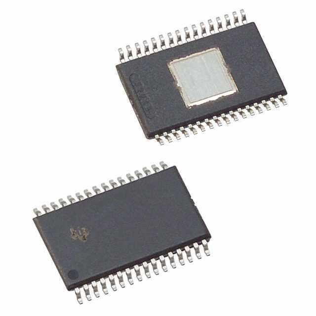
TLC5924 DAP RHB www.ti.com SLVS626–JUNE2006 16-CHANNEL LED DRIVER WITH DOT CORRECTION AND PRE-CHARGE FET FEATURES APPLICATIONS • 16Channels • Monocolor,Multicolor,FullcolorLEDDisplay • DriveCapability • Monocolor,MulticolorLEDSignboard – 0to80mA(Constant-CurrentSink) • DisplayBacklighting • ConstantCurrentAccuracy:±1%(typical) • MulticolorLEDlightingapplications • SerialDataInterface DESCRIPTION • FastSwitchingOutput:T /T =10ns(typical) r f The TLC5924 is a 16 channel constant-current sink • CMOSLevelInput/Output driver. Each channel has a On/Off state and a • 30MHzDataTransferRate 128-step adjustable constant current sink (dot • V =3.0Vto5.5V correction). The dot correction adjusts the brightness CC variations between LED, LED channels and other • OperatingTemperature=–40(cid:176) Cto85(cid:176) C LEDdrivers.Bothdot correction and On/Off state are • LEDSupplyVoltageupto17V accessible via a serial data interface. A single • 32-pinHTSSOP(PowerPAD™)andQFN external resistor sets the maximum current of all 16 Packages channels. • DotCorrection Each constant-current output has a pre-charge FET – 7bit(128Steps) that enables an improvement in image quality of the dynamic-driveLEDdisplay. – individualadjustableforeachchannel • ControlledIn-RushCurrent The TLC5924 features two error information circuits. The LED open detection (LOD) indicates a broken or • Pre-ChargeFET disconnected LED at an output terminal. The thermal • ErrorInformation error flag (TEF) indicates an over-temperature – LOD:LEDOpenDetection condition. – TEF:ThermalErrorFlag FUNCTIONAL BLOCK DIAGRAM VCC GNDPGND SCLK SIN MODE XLAT VUP BLANK VUP 0 1 MODE 1 0 LOD 0 ConstDanritv eCrurrent OUT0 Delay 0 x0 0 On/Off Register IREF MaCxu. rOreUnTtn 7−bit DC Registe0r On/Off 6 BLANK Input VUP Shift Register 1616 On/OLffO RDegister11 ConDsxetDa1lanriytv eCrurrent OUT1 15 0 112 7 7−bit DC Register 13 LDEe(DLteO OcDtpi)oenn DRCeSg hIinsifptteurt BLANK Temperature VUP Er(rTorE FFl)ag 1 0BLANK LOD 15 ConstDanritv eCrurrent OUT15 Delay XERR 111 On/Off Registe1r5 x15 0 1 7−bit DC Regi1s0te5r MODE 111 SOUT Pleasebeawarethatanimportantnoticeconcerningavailability,standardwarranty,anduseincriticalapplicationsofTexas Instrumentssemiconductorproductsanddisclaimerstheretoappearsattheendofthisdatasheet. PowerPADisatrademarkofTexasInstruments. PRODUCTIONDATAinformationiscurrentasofpublicationdate. Copyright©2006,TexasInstrumentsIncorporated Products conform to specifications per the terms of the Texas Instruments standard warranty. Production processing does not necessarilyincludetestingofallparameters.
TLC5924 www.ti.com SLVS626–JUNE2006 Thesedeviceshavelimitedbuilt-inESDprotection.Theleadsshouldbeshortedtogetherorthedeviceplacedinconductivefoam duringstorageorhandlingtopreventelectrostaticdamagetotheMOSgates. ORDERINGINFORMATION(1) T Package PartNumber(1) A 32-pin,HTSSOP,PowerPAD™ TLC5924DAP –40(cid:176) Cto85(cid:176) C 32-pin,5mmx5mmQFN TLC5924RHB (1) Forthemostcurrentpackageandorderinginformation,seethePackageOptionAddendumattheend ofthisdocument,orseetheTIwebsiteatwww.ti.com. ABSOLUTE MAXIMUM RATINGS (1)(2) TLC5924 UNIT V Supplyvoltage(2) –0.3to6 V CC V Pre-chargevoltage –0.3to16 V UP I Outputcurrent(dc) I toI 90 mA O (OUT0) (OUT15) V Inputvoltagerange(2) V ,V ,V ,V ,V ,V –0.3toV +0.3 V I (BLANK) (XLAT) (SCLK) (SIN) (MODE) (IREF) CC V ,V –0.3toV +0.3 V V Outputvoltagerange(2) (SOUT) (XERR) CC O V toV -0.3toV V (OUT0) (OUT15) UP HBM(JEDECJESD22-A114,HumanBodyModel) 2 kV ESDrating CDM(JEDECJESD22-C101,ChargedDeviceModel) 500 V T Storagetemperaturerange –40to150 °C stg Powerdissipationratingat(or HTSSOP(DAP) 42.54 mW/(cid:176) C above)TA=25(cid:176) C(3) QFN(RHB) 27.86 mW/(cid:176) C (1) Stressesbeyondthoselistedunderabsolutemaximumratingsmaycausepermanentdamagetothedevice.Thesearestressratings only,andfunctionaloperationofthedeviceattheseoranyotherconditionsbeyondthoseindicatedunderrecommendedoperating conditionsisnotimplied.Exposuretoabsolute-maximum-ratedconditionsforextendedperiodsmayaffectdevicereliability. (2) Allvoltagevaluesarewithrespecttonetworkgroundterminal. (3) SeeSLMA002formoreinformationaboutPowerPAD™ RECOMMENDED OPERATING CONDITIONS—DC Characteristics MIN NOM MAX UNIT V Supplyvoltage 3 5.5 V CC V Pre-chargevoltage 3 15 V UP V Voltageappliedtooutput,(Out0-Out15) V V O UP V High-levelinputvoltage 0.8VCC VCC V IH V Low-levelinputvoltage GND 0.2VCC V IL I High-leveloutputcurrent V =5VatSOUT –1 mA OH CC I Low-leveloutputcurrent V =5VatSOUT,XERR 1 mA OL CC I Constantoutputcurrent OUT0toOUT15 80 mA OLC T Operatingfree-airtemperaturerange -40 85 (cid:176) C A 2 SubmitDocumentationFeedback
TLC5924 www.ti.com SLVS626–JUNE2006 RECOMMENDED OPERATING CONDITIONS—AC Characteristics V =3Vto5.5V,T =-40°Cto85°C(unlessotherwisenoted) CC A MIN TYP MAX UNIT f Clockfrequency SCLK 30 MHz SCLK t ,t CLKpulseduration SCLK=H/L 16 ns wh0 wl0 t XLATpulseduration XLAT=H 20 ns wh1 t SIN to SCLK› (1) 10 su0 t SLCK› toXLATfl (dotcorrectiondata) 10 su1 t Setuptime SCLK› toXLAT› (ON/OFFdata) 10 ns su1a t MODE› fl toSCLK› 10 su2 t MODE› fl toXLAT› 10 su3 t SCLK› toSIN 10 h0 t XLATfl toSCLK› (dotcorrectiondata) 10 h1 t Holdtime XLAT› toSCLK› (ON/OFFdata) 10 ns h1a t SCLK›to MODE› fl 10 h2 t XLATfl toMODE› fl 10 h3 (1) "› "and"fl "indicatesarisingedge,andafallingedgerespectively. ELECTRICAL CHARACTERISTICS V =3Vto5.5V,T =–40(cid:176) Cto85(cid:176) C(unlessotherwisenoted) CC A PARAMETER TESTCONDITIONS MIN TYP MAX UNIT V High-leveloutputvoltage I =–1mA,SOUT V –0.5 V OH OH CC V Low-leveloutputvoltage I =1mA,SOUT 0.5 V OL OL I Inputcurrent V =V orGND,BLANK,XLAT,SCLK,SIN,MODE –1 1 m A I I CC Nodatatransfer,AlloutputOFF,V =1V,R =10 kW O (IREF) 6 Nodatatransfer,AlloutputOFF,V =1V,R =1.3 kW O (IREF) 15 I Supplycurrent mA CC Datatransfer30MHz,AlloutputON,V =1V, R =1.3kW O 32 (IREF) Datatransfer30MHz,AlloutputON,V =1V, R =600W O 36 65(1) (IREF) I Constantsinkcurrent AlloutputON,V =1V,R =600W 70 80 90 mA OLC O (IREF) I AlloutputOFF,VO=15V,R(IREF)=600W ,OUT0to 0.1 m A LO0 Leakageoutputcurrent OUT15 I V =5.5V,NoTEFandLOD 10 m A LO1 XERR D I Constantsinkcurrenterror AlloutputON,V =1V,R =600W ,OUT0toOUT15 – 1% – 4% OLC0 O (IREF) D IOLC1 Constantsinkcurrenterror dRevicet=o6d0e0viWce,averagedcurrentfromOUT0toOUT15, – 4% – 8.5% (IREF) D I Lineregulation AlloutputON,VO=1V,R(IREF)=600W , – 1 – 4 %/V OLC2 OUT0toOUT15,V =3Vto5.5V CC D I Loadregulation AlloutputON,VO=1Vto3V,R(IREF)=600W , – 2 – 6 %/V OLC3 OUT0toOUT15 R Pre-chargeFETon-resistance V =3V,V =0V,OUT0toOUT15 10 KW (ON) UP O T Thermalerrorflagthreshold Junctiontemperature,risingtemperature(2) 150 160 180 (cid:176) C (TEF) V LEDopendetectionthreshold 0.3 0.4 V (LOD) V Referencevoltageoutput R =600W 1.20 1.24 1.28 V (IREF) (IREF) (1) Measuredatdevicestart-uptemperature.OncetheICisoperating(selfheating),lowerI valueswillbeseen.SeeFigure20. CC (2) Nottested.Specifiedbydesign. SubmitDocumentationFeedback 3
TLC5924 www.ti.com SLVS626–JUNE2006 DISSIPATION RATINGS POWERRATING DERATINGFACTOR POWERRATING POWERRATING PACKAGE T <25(cid:176) C ABOVETA=25(cid:176) C T =70(cid:176) C T =85(cid:176) C A A A 32-pinHTSSOPwithPowerPAD(1) 5318mW 42.54mW/(cid:176) C 3403mW 2765mW soldered 32-pinHTSSOPwithPowerPAD(1) 2820mW 22.56mW/(cid:176) C 1805mW 1466mW unsoldered 32-pinQFN 3482mW 27.86mW/(cid:176) C 2228mW 1811mW (1) ThePowerPADissolderedtothePCBwitha2oz.coppertrace.SeeSLMA002forfurtherinformation. SWITCHING CHARACTERISTICS PARAMETER TESTCONDITIONS MIN TYP MAX UNIT t SOUT(see (1)) 16 r0 Risetime ns t OUTn,V =5V,T =60(cid:176) C,DCx=7F(see (2)) 10 30 r1 CC A t SOUT(see (1)) 16 f0 Falltime ns t OUTn,V =5V,T =60(cid:176) C,DCx=7F(see (2)) 10 30 f1 CC A t SCLK› to SOUT› fl (see (3)(4)) 30 pd0 t MODE›fl to SOUT› fl (see (3)) 30 pd1 t BLANK› fl to OUT0› fl (see (5)),SinkcurrentOn/Off 80 pd2 Propagationdelaytime ns t XLAT› to OUT0› fl (see (5)) 60 pd3 t OUTn› fl toXERR› fl (see (6)) 1000 pd4 t XLAT› toI (dot-correction)(see (7)) 1000 pd5 OUT t Outputdelaytime OUTn› toOUT(n+1)› ,OUTnfl toOUT(n+1)fl (see (5)) 14 22 30 ns d (1) SeeFigure4.Definedasfrom10%to90% (2) SeeFigure5.Definedasfrom10%to90% (3) SeeFigure4,Figure16 (4) "› "and"fl "indicatesarisingedge,andafallingedgerespectively. (5) SeeFigure5andFigure16 (6) SeeFigure5,Figure6,andFigure16 (7) SeeFigure5 RHB PACKAGE (TOP VIEW) DAP PACKAGE (TOP VIEW) T 15 14 D 13 12 11 U P T T N T T T O U U U G U U U S V O O P O O O GND 1 32 VCC 4 3 2 1 0 9 8 7 BLANK 2 31 IREF 2 2 2 2 2 1 1 1 XLAT 3 30 MODE SCLK 4 29 XERR XERR 25 16 OUT10 SIN 5 28 SOUT MODE 26 15 PGND VUP 6 27 VUP IREF 27 14 OUT9 THERMAL OUT0 7 26 OUT15 VCC 28 13 OUT8 OUT1 8 25 OUT14 PAD GND 29 12 OUT7 PGND 9 24 PGND (QFN) OUT2 10 23 OUT13 BLANK 30 11 OUT6 OUT3 11 22 OUT12 XLAT 31 10 PGND OUT4 12 21 OUT11 SCLK 32 9 OUT5 OUT5 13 20 OUT10 PGND 14 19 PGND 1 2 3 4 5 6 7 8 OUT6 15 18 OUT9 N P 0 1 D 2 3 4 OUT7 16 17 OUT8 SI VU UT UT GN UT UT UT O O P O O O 4 SubmitDocumentationFeedback
TLC5924 www.ti.com SLVS626–JUNE2006 TerminalFunctions TERMINAL NO. I/O DESCRIPTION NAME TSSOP QFN Blank(LightOFF).WhenBLANK=H,AllOUTnoutputsareforcedtoVUPlevel.When BLANK 2 30 I BLANK=L,ON/OFFofOUTnoutputsarecontrolledbyinputdata. GND 1 29 Ground IREF 31 27 I/O Referencecurrentterminal Modeselect.WhenMODE=L,SIN,SOUT,SCLK,XLATareconnectedtoON/OFFcontrol MODE 30 26 I logic.WhenMODE=H,SIN,SOUT,SCLK,XLATareconnectedtodot-correctionlogic. OUT0 7 3 O Constantcurrentoutput OUT1 8 4 O Constantcurrentoutput OUT2 10 6 O Constantcurrentoutput OUT3 11 7 O Constantcurrentoutput OUT4 12 8 O Constantcurrentoutput OUT5 13 9 O Constantcurrentoutput OUT6 15 11 O Constantcurrentoutput OUT7 16 12 O Constantcurrentoutput OUT8 17 13 O Constantcurrentoutput OUT9 18 14 O Constantcurrentoutput OUT10 20 16 O Constantcurrentoutput OUT11 21 17 O Constantcurrentoutput OUT12 22 18 O Constantcurrentoutput OUT13 23 19 O Constantcurrentoutput OUT14 25 21 O Constantcurrentoutput OUT15 26 22 O Constantcurrentoutput 9,14, 5,10, PGND Powerground 19,24 15,20 VUP 6,27 2,23 Pre-chargepowersupplyvoltage Datashiftclock.NotethattheinternalconnectionsareswitchedbyMODE(pin#30).At SCLK 4 32 I SCLK› ,theshift-registersselectedbyMODEshiftthedata. SIN 5 1 I DatainputofserialI/F SOUT 28 24 O DataoutputofserialI/F VCC 32 28 Powersupplyvoltage Erroroutput.XERRisopendrainterminal.XERRtransistionsfromHtoLwhenLODorTEF XERR 29 25 O detected. Datalatchsignal.WhenMODE=L(ON/OFFdatamode),XLATisanedge-triggeredlatch signalofON/OFFregisters.TheserialdatainON/OFFinputshiftregistersislatchedintothe ON/OFFregistersattherisingedgeofXLAT.WhenMODE=H(DCdatamode),XLATisa XLAT 3 31 I level-triggeredlatchsignalofdotcorrectionregisters.TheserialdatainDCinputshift registersiswrittenintodotcorrectionregisterswhenXLAT=H.Thedataindotcorrection registersisheldconstantwhenXLAT=L. SubmitDocumentationFeedback 5
TLC5924 www.ti.com SLVS626–JUNE2006 PIN EQUIVALENT INPUT AND OUTPUT SCHEMATIC DIAGRAMS (Note:Resistorvaluesareequivalentresistanceandnottested). VCC 400 (cid:1) INPUT GND Figure1.InputEquivalentCircuit(BLANK,XLAT,SCLK,SIN,MODE) 10 (cid:1) SOUT GND Figure2.OutputEquivalentCircuit 20 (cid:1) XERR GND Figure3.OutputEquivalentCircuit(XERR) PARAMETER MEASUREMENT INFORMATION SOUT 15 pF Figure4.TestCircuitfort ,t ,t ,t r0 f0 pd0 pd1 VUP 51Ω OUTn 15 pF Figure5.TestCircuitfort ,t ,t ,t ,t ,t r1 f1 pd2 pd3 pd5 td 6 SubmitDocumentationFeedback
TLC5924 www.ti.com SLVS626–JUNE2006 PARAMETER MEASUREMENT INFORMATION (continued) 470 kW XERR Figure6.TestCircuitfort pd4 SubmitDocumentationFeedback 7
TLC5924 www.ti.com SLVS626–JUNE2006 PRINCIPLES OF OPERATION Setting Maximum Channel Current The maximum output current per channel is set by a single external resistor, R , which is placed between (IREF) IREF and GND. The voltage on IREF is set by an internal band gap V with a typical value of 1.24V. The (IREF) maximum channel current is equivalent to the current flowing through R multiplied by a factor of 40. The (IREF) maximumoutputcurrentperchannelcanbecalculatedbyEquation1: V I (cid:2) IREF (cid:1)40 MAX R IREF (1) where: V =1.24Vtyp. IREF R =Userselectedexternalresistor® shouldnotbesmallerthan600W) IREF IREF Figure 17 shows the maximum output current, I , versus R . In Figure 17, R is the value of the OLC (IREF) (IREF) resistor between IREF terminal to ground, and I is the constant output current of OUT0,.....OUT15. A variable OLC power supply may be connected to the IREF pin through a resistor to change the maximum output current per channel. The maximum output per channel is 40 times the current flowing out of the IREF pin. The maximum currentfromIREFequals1.24V/600W . Setting Dot-Correction The TLC5924 has the capability to fine adjust the current of each channel, OUT0 to OUT15 independently. This is also called dot correction. This feature is used to adjust the brightness deviations of LED connected to the output channels OUT0 to OUT15. Each of the 16 channels can be programmed with a 7-bit word. The channel output can be adjusted in 128 steps from 0% to 100% of the maximum output current I . Dot correction for all MAX channelsmustbeenteredatthesametime.Equation2determinestheoutputcurrentforeachOUTn: I (cid:1) DC I (cid:2) MAX n Outn 127 (2) where: I =themaximumprogrammablecurrentofeachoutput Max DCn=theprogrammeddot-correctionvalueforoutputn(DCn=0,1,2...127) n=0,1,2...15 Dot correction data are entered for all channels at the same time. The complete dot correction data format consists of 16 x 7-bit words, which forms a 112-bit wide serial data packet. The channel data is put one after another.AlldataisclockedinwithMSBfirst.Figure7showstheDCdataformat.TheDC15.6 in Figure 7 stands forthe6thmostsignificantbitforoutput15. MSB LSB 111 105 104 7 6 0 DC 15.6 DC 15.0 DC 14.6 DC 1.0 DC 0.6 DC 0.0 DC OUT15 DC OUT14−DC OUT1 DC OUT0 Figure7.DCDataFormat To input data into dot correction register, MODE must be set to high. The internal input shift register is then set to 112-bit width. After all serial data is clocked in, a high level pulse of XLAT signal connects the serial data to the dot correction register. The dot correction registers are level-triggered latches of XLAT signal. The serial data is latched into the dot correction registers when XLAT goes low. The data in dot correction registers is held constant when XLAT is low. BLANK signal does not need to be high to latch in new data. Since XLAT is a level-triggeredsignalwhenMODEishigh,SCLKandSINmustnotbechangedwhileXLATishigh.(Figure16). 8 SubmitDocumentationFeedback
TLC5924 www.ti.com SLVS626–JUNE2006 PRINCIPLES OF OPERATION (continued) Output Enable When BLANK = H, TLC5924 switches off the sink current of all OUTn with each output delay, then switches on thepre-chargeFETofallOUTn.WhenBLANK=L,theTLC5924switchesoffthepre-chargeFETs, and enables thesinkcurrentsetbyinputdata.See"DelayBetweenOutputs"sectionformoredetailontheoutputdelay. Table1.BLANKSignalTruthTable BLANK OUT0-OUT15 LOW Normalcondition HIGH VUP Setting Channel On/Off Status All OUTn channels of TLC5924 can be switched on or off independently. Each of the channels can be programmed with a 1-bit word. On/Off data are entered for all channels at the same time. The complete On/Off data format consists of 16 x 1-bit words, which form a 16-bit wide data packet. The channel data is put one after another.AlldataisclockedinwithMSBfirst.Figure8showstheOn/Offdataformat. MSB LSB 15 0 On/Off On/Off On/Off On/Off On/Off On/Off OUT15 OUT14 OUT13 OUT2 OUT1 OUT0 On/Off Data Figure8.On/OffDataFormat To input On/Off data into On/Off register MODE must be set to low. The internal input shift register is then set to 16 bit width. After all serial data is clocked in, a rising edge of XLAT is used to latch data into the On/Off register.TheON/OFFregisterisanedge-triggeredlatch of XLAT signal. BLANK signal does not need to be high tolatchinnewdata.Figure16showstheOn/Offdatainputtimingchart. Delay Between Outputs The TLC5924 has graduated delay circuits between outputs. These delay circuits can be found in the constant current block of the device (see Functional Block Diagram). The fixed delay time is 20 ns (typical), OUT0 has no delay, OUT1 has 20 ns delay, OUT2 has 40 ns delay, etc. This delay prevents large inrush currents, which reducepowersupplybypasscapacitorrequirementswhentheoutputsturnon.Thedelay works during switch on andswitchoffofeachoutputchannel.LEDsthathavenotturnedonbeforeBLANKispulledhigh will still turn on and off at the determined delayed time regardless of the state of BLANK. Therefore, every LED will be illuminatedfortheamountoftimeBLANKislow. Pre-Charge FET On/Off Timing Thepre-chargeFETsturnonatthesametime;and,theyturnonatthetimethelastoutputthatisonturnsoff. All pre-charge FETs turn off just after BLANK signal becomes low level, regardless of on/off data of each output. Figure9showstheexampleofBLANKandOUTntiming. SubmitDocumentationFeedback 9
TLC5924 www.ti.com SLVS626–JUNE2006 BLANK VUP OUT0 Current ON OFF ON t t pd2 pd2 t x 14 t x 14 d d OUT14 OFF ON OUT15 Pre-charge Period Figure9.TimingChartofBLANKandOUTn (On/OffDataCondition:OUT0=H,OUT14=H,OUT15=L) VUP: Pre-Charge Power Supply VUP is a pre-charge power supply terminal. The pre-charge voltage should be supplied to this terminal for normal operation. When VUP terminal is open, TLC5924 keeps OUT0-15 open. TLC5924 has two VUP pins as shown in the Terminal Functions Table. Both VUP pins should be connected to the pre-charge power supply as showninFigure10. Pre-Charge Power Supply VUP VUP TLC5924 Figure10.VUPPowerSupply Serial Interface Data Transfer Rate The TLC5924 includes a flexible serial interface, which can be connected to a microcontroller or digital signal processor. Only 3 pins are required to input data into the device. The rising edge of SCLK signal shifts the data from SIN pin to internal shift register. After all data is clocked in, a rising edge of XLAT latches the serial data to the internal registers. All data is clocked in with MSB first. Multiple TLC5924 devices can be cascaded by connecting SOUT pin of one device with SIN pin of following device. The SOUT pin can also be connected to controllertoreceiveLODinformationfromTLC5924. 10 SubmitDocumentationFeedback
TLC5924 www.ti.com SLVS626–JUNE2006 VCC V(LED) V(LED) V(LED) V(LED) 100 k OUT0 OUT15 OUT0 OUT15 SIN SIN SOUT SIN SOUT XERR XERR VCC XERR VCC SCLK SCLK SCLK XLAT XLAT 100 nF XLAT 100 nF Controller MODE MODE TLC5924 MODE TLC5924 BLANK BLANK IREF BLANK IREF SOUT IC 0 IC n 5 Figure11.CascadingDevices Figure 11 shows a example application with n cascaded TLC5924 devices connected to a controller. The maximum number of cascaded TLC5924 devices depends on application system and data transfer rate. Equation3calculatestheminimumdatainputfrequencyneeded. f_(SCLK)(cid:2)112 (cid:1)f_(update) (cid:1) n (3) where: f_(SCLK):TheminimumdatainputfrequencyforSCLKandSIN. f_(update):Theupdaterateofthewholecascadedsystem. n:ThenumberofcascadedTLC5924devices. Operating Modes The TLC5924 has different operating modes depending on MODE signal. Table 2 shows the available operating modes. The values in the input shift registers, DC register and On/Off register are unknown just after power on. The DC and On/Off register values should be properly stored through the serial interface before starting the operation. Table2.TLC5924OperatingModesTruthTable MODESIGNAL INPUTSHIFTREGISTER MODE LOW 16bit On/OffMode HIGH 112bit DotCorrectionDataInputMode SubmitDocumentationFeedback 11
TLC5924 www.ti.com SLVS626–JUNE2006 Error Information Output The open-drain output XERR is used to report both of the TLC5924 error flags, TEF and LOD. During normal operating conditions, the internal transistor connected to the XERR pin is turned off. The voltage on XERR is pulled up to V through a external pull-up resistor. If TEF or LOD is detected, the internal transistor is turned CC on, and XERR is pulled to GND. Since XERR is an open-drain output, multiple ICs can be OR'ed together and pulled up to V with a single pull-up resistor. This reduces the number of signals needed to report a system CC error. TodifferentiateLODandTEFsignalfromXERRpin,LODcanbemaskedoutwithBLANK=HIGH. Table3.XERRTruthTable CONDITION ERRORINFORMATION XERR TEMPERATURE BLANK OUTnVOLTAGE TEF LODn T <T H Don'tCare L L High-Z(1) J (TEF) T >T H L J (TEF) T <T L OUTn>V L L High-Z J (TEF) (LOD) OUTn<V H L (LOD) T >T OUTn>V H L L J (TEF) (LOD) OUTn<V H L (LOD) (1) Note:High-Zmeanshighimpedance TEF: Thermal Error Flag The TLC5924 provides a temperature error flag (TEF) circuit to indicate an over-temperature condition of the IC. If the junction temperature exceeds the threshold temperature T (160°C typical), TEF becomes H and XERR (TEF) pin goes to low level. When the junction temperature becomes lower than the threshold temperature, TEF becomesLandXERRpinbecomeshighimpedance. LOD: LED-Open Detection The TLC5924 has an LED-open detector to detect broken or disconnected LEDs, which should be connected to the output. The LED-open detector pulls the XERR pin down to GND when the LED open is detected. An open LEDisdetectedwhenthefollowingthreeconditionsaremet: 1. BLANKislow 2. On/Offdataishigh 3. ThevoltageofOUTnislessthan0.3V(typical) The LOD status of each output can also be read out from the SOUT pin. Figure 12 shows the LOD data format. Table4showstheLODtruthtable. MSB LSB 15 0 LOD LOD LOD LOD LOD LOD OUT15 OUT14 OUT13 OUT2 OUT1 OUT0 LOD Data Figure12.LODDataFormat 12 SubmitDocumentationFeedback
TLC5924 www.ti.com SLVS626–JUNE2006 Table4.LODDataTruthTable LED ON/OFF LODBIT Good On 0 Good Off 0 Bad On 1 Bad Off 0 KeyTimingRequirementstoReadingLOD • LODstatusflag The LOD status flag becomes active if the output voltage is <0.3 V (typical) when the output sink current turns on. There is a 1-µs time delay from the time the output sink current turns on until the time the LOD status flag becomes valid. The timing for each channel’s LOD status to become valid is shifted by the 30 ns channel-to-channel turn-on time. After BLANK goes low, OUT0 LOD status is valid when tpd2 + tpd4 = 60 ns + 1 µs = 1.06 µs. OUT1 LOD status is valid when tpd2 + tpd4 + td = 60 ns + 1 µs + 30 ns = 1.09 µs. OUT3LODstatusisvalidwhentpd2+tpd4+2*td=1.12µs,andsoon. • LODinternallatch The TLC5924 has an internal latch to hold each channel’s LOD status flag information, as shown in Figure 13. When MODE is low, the LOD status information is latched into this latch on the rising edge of XLAT.Thisisanedge-triggeredlatch.Toensure that a valid LOD status flag is latched, BLANK must be low when XLAT goes high. After the rising edge of XLAT, changes in the status flags do not affect the values in theLODlatch. • LoadingLODdatatotheinputshiftregister The LOD data must be transferred to the input shift register before it is available to be clocked out of SOUT. The internal shift register has a set/reset function that is controlled by the LOD internal latch. While XLAT is high, the LOD internal latch holds the input shift register in either set or reset, depending on the value in the latch. This effectively puts the LOD data into the input shift register where it remains as long as XLAT is high.Thevaluesintheinputshiftregisterareunaffectedbyanyothersignals,includingSIN and SCLK while XLATishigh.Duringthistime,thestatusofOUT15ispresentonSOUT. • LatchingLODdataintotheinternalshiftregister WhileXLATishigh,thestatusofOUT15ispresentonSOUT.WhenXLAT transitions low, all data is latched intotheInputshiftregister,andtheLODinternallatchisdisconnectedfromtheinternalshiftregister. • ClockingLODdataoutofSOUT While XLAT is low and SCLK is low, the status of OUT15 is on SOUT. On the next rising edge of SCLK, the status of OUT14 shifts to SOUT. Each subsequent rising edge of SCLK shifts the LOD data out of SOUT. XLAT must stay low until all LOD data is clocked out of SOUT. See Shifting the LOD Data Out section for moredetails. SubmitDocumentationFeedback 13
TLC5924 www.ti.com SLVS626–JUNE2006 16bit LOD Status Flags 16bit LOD Internal Latch SIN Input Shift Register SOUT (FIFO Register) GS Register Figure13.LODFlagsandLatches ShiftingtheLODDataOut SOUToutputstheLODdataasshowninFigure14,where: • XLATrisingedge HoldstheLODstatusflag.SOUToutputsLODOUT15data.BLANKmustbelow. • XLAT=H SetsorresetstheinputshiftregisterdependingoneachLODdata. Set/Reset function is higher priority than shifting the register value. If XLAT is high and the SCLK pin is pulsed,allLODdataarekeptintheshiftregisterandSOUTkeepstheLODOUT15data. • XLAT=L Ready to shift out LOD data by SCLK. SOUT contains LOD OUT15 data at this time. BLANK can be high or lowduringthistime. • SCLKrisingedge SOUT outputs LOD OUT14 at the first SCLK rising edge. SOUT outputs LOD OUT13 at the second SCLK risingedge,andcontinuestooutputthenextLODdataateachSCLKrisingedge. XLAT SCLK LOD LOD LOD LOD SOUT OUT15 OUT14 OUT13 OUT12 Figure14.TheLODDataofSOUT 14 SubmitDocumentationFeedback
TLC5924 www.ti.com SLVS626–JUNE2006 Figure15showsthetimingchartofreadingLODdata. At the rising edge of XLATwhile BLANK=L, LOD status is latched into MODE the internal edge-triggered register. When XLAT=H, the internal edge-triggered register sets or resets the input shift registe.r XLAT SCLK SIN SOUT 1510ns max 1510ns max BLANK tpd2: 60ns max tpd2: 60ns max OUT0 LED open OUT15 td x 15 = 450ns max td x 15 = 450ns max XERR tpd4: 1000ns max tpd4: 1000ns max >1000ns >1000ns Figure15.TimingChartofReadingLODData SubmitDocumentationFeedback 15
TLC5924 www.ti.com SLVS626–JUNE2006 Off Mode Datanput Cycle n/OffOn/OffMSBMSB−1 th1a On/OffMSB tpd4 n/I O O OffB n/MS OffSB O n/L O ata td On/Off Mode DInput Cycle tsu3 OffSB tsu1atsu2 1 On/fOfLSB On/M tpd On/OffMSB tpd5 CB CSB DS DM L 3 ut h de Data InpCycle t th0th2 tsu1d0 DCLSB o p DC M DCMSB th1 t tpd5 B CS e DCLSB tsu0 DM cl Cy K put SCL DCLSB n f ata I u3 D s DC Mode t DCMSB twl0 h0 tpd1 DCMSB tpd2 td w t 3 2 Off Mode Datanput Cycle twh1 th On/fOfLSB On/OffMSB tpd tpd3 n/I O nt) nt) MODE XLAT SIN SCLK SOUT BLANK XERR OUT0(curre OUT1(curre Figure16.TimingChartExampleforON/OFFSettingtoDot-Correction 16 SubmitDocumentationFeedback
TLC5924 www.ti.com SLVS626–JUNE2006 TYPICAL CHARACTERISTICS REFERENCERESISTOR OUTPUTCURRENT vs vs OUTPUTCURRENT REQUIREDOUTPUTnVOLTAGE 100 k 100 90 49.6 k VOutn = 1 V DC = 127 80 A m − W − 70 or 10 k 9.92 k nt IMAX= 60 mA st e 60 esi 4.96 k urr R C ence 2.48 k1.65 k utput 4500 IMAX= 40 mA er 1.24 k O − RefF 1 k 992 827709 I−O 30 IMAX= 20 mA RE 20 RI 10 100 0 0 0.01 0.02 0.03 0.04 0.05 0.06 0.07 0.08 0 0.50 1 1.50 2 2.50 3 IOLC − Output Current − A VO−Required Output Voltage−V Figure17. Figure18. POWERDISSIPATION SUPPLYCURRENT(A) vs vs FREE-AIRTEMPERATURE FREE-AIRTEMPERATURE 6 k 70 5 k TLC5924DAP 60 PowerPAD Soldered W m A m pation− 4 k TLC5924RHB urrent − 4500 Dissi 3 k ply C r p 30 we TLC5924DAP Su Po 2 k PowerPAD Unsoldered − C −D C 20 P I 1 k 10 0 0 −40 −20 0 20 40 60 80 100 −50 −30 −10 10 30 50 70 90 110 130 150 TA−Free-Air Temperature−°C TA − Free-Air Temperature − °C Figure19. A. Data Transfer = 30 MHz / All Outputs, ON/V =1V/R =600W /AV =5V O IREF DD Figure20. Power Rating – Free-Air Temperature Figure19showstotalpowerdissipation.Figure20showssupplycurrentversusfree-airtemperature. SubmitDocumentationFeedback 17
PACKAGE OPTION ADDENDUM www.ti.com 6-Feb-2020 PACKAGING INFORMATION Orderable Device Status Package Type Package Pins Package Eco Plan Lead/Ball Finish MSL Peak Temp Op Temp (°C) Device Marking Samples (1) Drawing Qty (2) (6) (3) (4/5) TLC5924DAP ACTIVE HTSSOP DAP 32 46 Green (RoHS NIPDAU Level-3-260C-168 HR -40 to 85 TLC5924 & no Sb/Br) TLC5924DAPR ACTIVE HTSSOP DAP 32 2000 Green (RoHS NIPDAU Level-3-260C-168 HR -40 to 85 TLC5924 & no Sb/Br) TLC5924RHBR ACTIVE VQFN RHB 32 3000 Green (RoHS NIPDAU Level-2-260C-1 YEAR -40 to 85 TLC & no Sb/Br) 5924 TLC5924RHBT ACTIVE VQFN RHB 32 250 Green (RoHS NIPDAU Level-2-260C-1 YEAR -40 to 85 TLC & no Sb/Br) 5924 TLC5924RHBTG4 ACTIVE VQFN RHB 32 250 Green (RoHS NIPDAU Level-2-260C-1 YEAR -40 to 85 TLC & no Sb/Br) 5924 (1) The marketing status values are defined as follows: ACTIVE: Product device recommended for new designs. LIFEBUY: TI has announced that the device will be discontinued, and a lifetime-buy period is in effect. NRND: Not recommended for new designs. Device is in production to support existing customers, but TI does not recommend using this part in a new design. PREVIEW: Device has been announced but is not in production. Samples may or may not be available. OBSOLETE: TI has discontinued the production of the device. (2) RoHS: TI defines "RoHS" to mean semiconductor products that are compliant with the current EU RoHS requirements for all 10 RoHS substances, including the requirement that RoHS substance do not exceed 0.1% by weight in homogeneous materials. Where designed to be soldered at high temperatures, "RoHS" products are suitable for use in specified lead-free processes. TI may reference these types of products as "Pb-Free". RoHS Exempt: TI defines "RoHS Exempt" to mean products that contain lead but are compliant with EU RoHS pursuant to a specific EU RoHS exemption. Green: TI defines "Green" to mean the content of Chlorine (Cl) and Bromine (Br) based flame retardants meet JS709B low halogen requirements of <=1000ppm threshold. Antimony trioxide based flame retardants must also meet the <=1000ppm threshold requirement. (3) MSL, Peak Temp. - The Moisture Sensitivity Level rating according to the JEDEC industry standard classifications, and peak solder temperature. (4) There may be additional marking, which relates to the logo, the lot trace code information, or the environmental category on the device. (5) Multiple Device Markings will be inside parentheses. Only one Device Marking contained in parentheses and separated by a "~" will appear on a device. If a line is indented then it is a continuation of the previous line and the two combined represent the entire Device Marking for that device. (6) Lead/Ball Finish - Orderable Devices may have multiple material finish options. Finish options are separated by a vertical ruled line. Lead/Ball Finish values may wrap to two lines if the finish value exceeds the maximum column width. Addendum-Page 1
PACKAGE OPTION ADDENDUM www.ti.com 6-Feb-2020 Important Information and Disclaimer:The information provided on this page represents TI's knowledge and belief as of the date that it is provided. TI bases its knowledge and belief on information provided by third parties, and makes no representation or warranty as to the accuracy of such information. Efforts are underway to better integrate information from third parties. TI has taken and continues to take reasonable steps to provide representative and accurate information but may not have conducted destructive testing or chemical analysis on incoming materials and chemicals. TI and TI suppliers consider certain information to be proprietary, and thus CAS numbers and other limited information may not be available for release. In no event shall TI's liability arising out of such information exceed the total purchase price of the TI part(s) at issue in this document sold by TI to Customer on an annual basis. Addendum-Page 2
PACKAGE MATERIALS INFORMATION www.ti.com 14-Feb-2019 TAPE AND REEL INFORMATION *Alldimensionsarenominal Device Package Package Pins SPQ Reel Reel A0 B0 K0 P1 W Pin1 Type Drawing Diameter Width (mm) (mm) (mm) (mm) (mm) Quadrant (mm) W1(mm) TLC5924DAPR HTSSOP DAP 32 2000 330.0 24.4 8.6 11.5 1.6 12.0 24.0 Q1 TLC5924RHBR VQFN RHB 32 3000 330.0 12.4 5.3 5.3 1.5 8.0 12.0 Q2 TLC5924RHBT VQFN RHB 32 250 180.0 12.4 5.3 5.3 1.5 8.0 12.0 Q2 PackMaterials-Page1
PACKAGE MATERIALS INFORMATION www.ti.com 14-Feb-2019 *Alldimensionsarenominal Device PackageType PackageDrawing Pins SPQ Length(mm) Width(mm) Height(mm) TLC5924DAPR HTSSOP DAP 32 2000 350.0 350.0 43.0 TLC5924RHBR VQFN RHB 32 3000 367.0 367.0 35.0 TLC5924RHBT VQFN RHB 32 250 210.0 185.0 35.0 PackMaterials-Page2
GENERIC PACKAGE VIEW RHB 32 VQFN - 1 mm max height 5 x 5, 0.5 mm pitch PLASTIC QUAD FLATPACK - NO LEAD Images above are just a representation of the package family, actual package may vary. Refer to the product data sheet for package details. 4224745/A www.ti.com
PACKAGE OUTLINE RHB0032E VQFN - 1 mm max height SCALE 3.000 PLASTIC QUAD FLATPACK - NO LEAD A 5.1 B 4.9 PIN 1 INDEX AREA 5.1 (0.1) 4.9 SIDE WALL DETAIL OPTIONAL ME20.000TAL THICKNESS C 1 MAX SEATING PLANE 0.05 0.00 0.08 C 2X 3.5 3.45 0.1 (0.2) TYP 9 16 EXPOSED THERMAL PAD 28X 0.5 8 17 SEE SIDE WALL DETAIL 2X 33 SYMM 3.5 0.3 32X 0.2 24 0.1 C A B 1 0.05 C 32 25 PIN 1 ID SYMM (OPTIONAL) 0.5 32X 0.3 4223442/B 08/2019 NOTES: 1. All linear dimensions are in millimeters. Any dimensions in parenthesis are for reference only. Dimensioning and tolerancing per ASME Y14.5M. 2. This drawing is subject to change without notice. 3. The package thermal pad must be soldered to the printed circuit board for thermal and mechanical performance. www.ti.com
EXAMPLE BOARD LAYOUT RHB0032E VQFN - 1 mm max height PLASTIC QUAD FLATPACK - NO LEAD ( 3.45) SYMM 32 25 32X (0.6) 1 24 32X (0.25) (1.475) 28X (0.5) 33 SYMM (4.8) ( 0.2) TYP VIA 8 17 (R0.05) TYP 9 16 (1.475) (4.8) LAND PATTERN EXAMPLE SCALE:18X 0.07 MAX 0.07 MIN ALL AROUND ALL AROUND SOLDER MASK METAL OPENING SOLDER MASK METAL UNDER OPENING SOLDER MASK NON SOLDER MASK SOLDER MASK DEFINED DEFINED (PREFERRED) SOLDER MASK DETAILS 4223442/B 08/2019 NOTES: (continued) 4. This package is designed to be soldered to a thermal pad on the board. For more information, see Texas Instruments literature number SLUA271 (www.ti.com/lit/slua271). 5. Vias are optional depending on application, refer to device data sheet. If any vias are implemented, refer to their locations shown on this view. It is recommended that vias under paste be filled, plugged or tented. www.ti.com
EXAMPLE STENCIL DESIGN RHB0032E VQFN - 1 mm max height PLASTIC QUAD FLATPACK - NO LEAD 4X ( 1.49) (R0.05) TYP (0.845) 32 25 32X (0.6) 1 24 32X (0.25) 28X (0.5) (0.845) SYMM 33 (4.8) 8 17 METAL TYP 9 16 SYMM (4.8) SOLDER PASTE EXAMPLE BASED ON 0.125 mm THICK STENCIL EXPOSED PAD 33: 75% PRINTED SOLDER COVERAGE BY AREA UNDER PACKAGE SCALE:20X 4223442/B 08/2019 NOTES: (continued) 6. Laser cutting apertures with trapezoidal walls and rounded corners may offer better paste release. IPC-7525 may have alternate design recommendations. www.ti.com
GENERIC PACKAGE VIEW DAP 32 PowerPADTM TSSOP - 1.2 mm max height 8.1 x 11, 0.65 mm pitch PLASTIC SMALL OUTLINE This image is a representation of the package family, actual package may vary. Refer to the product data sheet for package details. 4225303/A www.ti.com
None
None
None
IMPORTANTNOTICEANDDISCLAIMER TI PROVIDES TECHNICAL AND RELIABILITY DATA (INCLUDING DATASHEETS), DESIGN RESOURCES (INCLUDING REFERENCE DESIGNS), APPLICATION OR OTHER DESIGN ADVICE, WEB TOOLS, SAFETY INFORMATION, AND OTHER RESOURCES “AS IS” AND WITH ALL FAULTS, AND DISCLAIMS ALL WARRANTIES, EXPRESS AND IMPLIED, INCLUDING WITHOUT LIMITATION ANY IMPLIED WARRANTIES OF MERCHANTABILITY, FITNESS FOR A PARTICULAR PURPOSE OR NON-INFRINGEMENT OF THIRD PARTY INTELLECTUAL PROPERTY RIGHTS. These resources are intended for skilled developers designing with TI products. You are solely responsible for (1) selecting the appropriate TI products for your application, (2) designing, validating and testing your application, and (3) ensuring your application meets applicable standards, and any other safety, security, or other requirements. These resources are subject to change without notice. TI grants you permission to use these resources only for development of an application that uses the TI products described in the resource. Other reproduction and display of these resources is prohibited. No license is granted to any other TI intellectual property right or to any third party intellectual property right. TI disclaims responsibility for, and you will fully indemnify TI and its representatives against, any claims, damages, costs, losses, and liabilities arising out of your use of these resources. TI’s products are provided subject to TI’s Terms of Sale (www.ti.com/legal/termsofsale.html) or other applicable terms available either on ti.com or provided in conjunction with such TI products. TI’s provision of these resources does not expand or otherwise alter TI’s applicable warranties or warranty disclaimers for TI products. Mailing Address: Texas Instruments, Post Office Box 655303, Dallas, Texas 75265 Copyright © 2020, Texas Instruments Incorporated