ICGOO在线商城 > TLC5904PZP
 Datasheet下载
- 型号: TLC5904PZP
- 制造商: Texas Instruments
- 库位|库存: xxxx|xxxx
- 要求:
| 数量阶梯 | 香港交货 | 国内含税 |
| +xxxx | $xxxx | ¥xxxx |
查看当月历史价格
查看今年历史价格
TLC5904PZP产品简介:
ICGOO电子元器件商城为您提供TLC5904PZP由Texas Instruments设计生产,在icgoo商城现货销售,并且可以通过原厂、代理商等渠道进行代购。 提供TLC5904PZP价格参考¥33.73-¥62.67以及Texas InstrumentsTLC5904PZP封装/规格参数等产品信息。 你可以下载TLC5904PZP参考资料、Datasheet数据手册功能说明书, 资料中有TLC5904PZP详细功能的应用电路图电压和使用方法及教程。
| 参数 | 数值 |
| 产品目录 | 集成电路 (IC)光电子产品 |
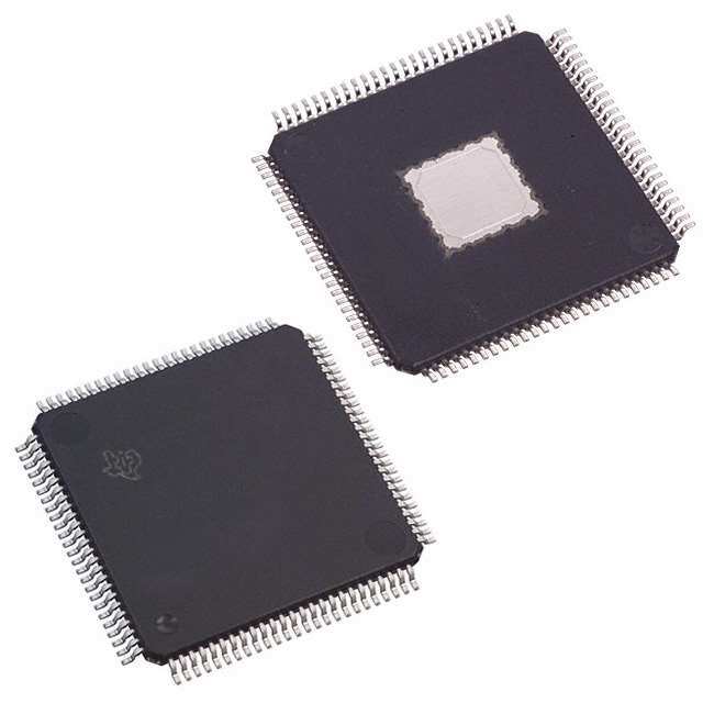
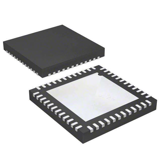
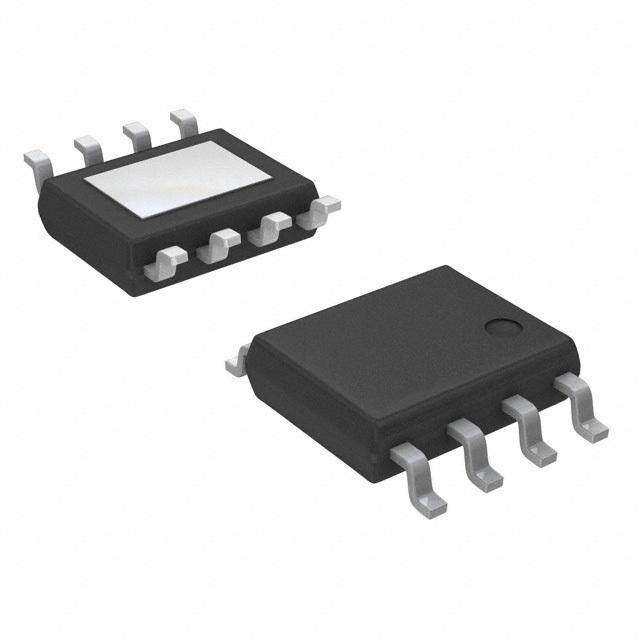
| 描述 | IC LED DRIVER LINEAR 100-TQFPLED照明驱动器 LED DRIVER |
| 产品分类 | |
| 品牌 | Texas Instruments |
| 产品手册 | |
| 产品图片 |
|
| rohs | 符合RoHS无铅 / 符合限制有害物质指令(RoHS)规范要求 |
| 产品系列 | LED照明电子器件,LED照明驱动器,Texas Instruments TLC5904PZP- |
| 数据手册 | |
| 产品型号 | TLC5904PZP |
| PCN组件/产地 | |
| 产品目录页面 | |
| 产品种类 | LED照明驱动器 |
| 低电平输出电流 | 1 mA |
| 供应商器件封装 | 100-HTQFP(14x14) |
| 其它名称 | 296-2378 |
| 内部驱动器 | 是 |
| 功率耗散 | 4.7 W |
| 包装 | 托盘 |
| 单位重量 | 505.400 mg |
| 商标 | Texas Instruments |
| 安装类型 | 表面贴装 |
| 安装风格 | SMD/SMT |
| 封装 | Tube |
| 封装/外壳 | 100-TQFP 裸露焊盘 |
| 封装/箱体 | HTQFP-100 |
| 工作温度 | -20°C ~ 85°C |
| 工作频率 | 15 MHz |
| 工厂包装数量 | 90 |
| 恒压 | - |
| 恒流 | 是 |
| 拓扑 | 线性 |
| 拓扑结构 | Boost |
| 最大工作温度 | + 85 C |
| 最大电源电流 | 70 mA |
| 最小工作温度 | - 20 C |
| 标准包装 | 90 |
| 电压-电源 | 4.5 V ~ 5.5 V |
| 电压-输出 | 17V |
| 类型 | Linear |
| 类型-初级 | 通用 |
| 类型-次级 | - |
| 系列 | TLC5904 |
| 输入电压 | 4.5 V to 5.5 V |
| 输出数 | 16 |
| 输出电流 | 80 mA |
| 输出端数量 | 16 Output |
| 输出类型 | Constant Current |
| 频率 | 15MHz |
| 高电平输出电流 | - 1 mA |

.jpg)


- 商务部:美国ITC正式对集成电路等产品启动337调查
- 曝三星4nm工艺存在良率问题 高通将骁龙8 Gen1或转产台积电
- 太阳诱电将投资9.5亿元在常州建新厂生产MLCC 预计2023年完工
- 英特尔发布欧洲新工厂建设计划 深化IDM 2.0 战略
- 台积电先进制程称霸业界 有大客户加持明年业绩稳了
- 达到5530亿美元!SIA预计今年全球半导体销售额将创下新高
- 英特尔拟将自动驾驶子公司Mobileye上市 估值或超500亿美元
- 三星加码芯片和SET,合并消费电子和移动部门,撤换高东真等 CEO
- 三星电子宣布重大人事变动 还合并消费电子和移动部门
- 海关总署:前11个月进口集成电路产品价值2.52万亿元 增长14.8%


PDF Datasheet 数据手册内容提取
TLC5904 LED DRIVER SLLS391 – NOVEMBER 1999 (cid:0) (cid:0) Drive Capability and Output Counts Data Output Timing Selectable – 80 mA (Current Sink) x 16 Bits – Select Data Output Timing for Shift – 120 mA (Current Sink) x 8 Bits Register Relative to Clock (cid:0) (cid:0) Constant Current Output Range OVM (Output Voltage Monitor) – 5 to 80 mA/10 to 120mA (Selectable by – Monitor Voltage on Constant Current MODE Terminal) (Current Value Setting for Output Terminals (Detect LED All Output Terminals Using External Disconnection and Short Circuit) Resistor and Internal Brightness Control (cid:0) WDT (Watchdog Timer) Register) – Turn Output Off When Scan Signal (cid:0) Constant Current Accuracy Stopped – ±4% (Maximum Error Between Bits) (cid:0) TSD (Thermal ShutDown) (cid:0) Voltage Applied to Constant Current Output – Turn Output Off When Junction Terminals Temperature Exceeds Limit – Minimum 0.4 V (Output Current 5 mA to (cid:0) Data Input 40 mA) – Clock Synchronized 8 Bit Parallel Input – Minimum 0.7 V (Output Current 40 to (Schmitt-Triggered Input) 80 mA) (cid:0) Data Output (cid:0) 256 Gray Scale Display – Clock Synchronized 8 Bit Parallel Output – Pulse Width Control 256 Steps (3-State Output) (cid:0) Brightness Adjustment (cid:0) Input Signal Level...CMOS Level – Output Current Adjustment for 32 Steps (cid:0) Power Supply Voltage...4.5 V to 5.5 V (Adjustment for Brightness Deviation (cid:0) Maximum Output Voltage...17 V (Max) Between LED Modules) (cid:0) – 8 Steps Brightness Control by 8 Times Data Transfer Rate...15 MHz (Max) Speed Gray Scale Control Clock (cid:0) Gray Scale Clock Frequency (Brightness Adjustment for Panel) 8 MHz (Max) (cid:0) Error Output Signal Check (cid:0) Operating Free-Air Temperature Range – Check Error Output Signal Line Such as –20(cid:1)C to 85(cid:1)C Protection Circuit When Operating (cid:0) 100-Pin HTQFP Package (P =4.7 W, D TA = 25°C) description The TLC5904 is a constant current driver incorporating shift register, data latch, and constant current circuitry with current value adjustable and a 256 gray scale display using pulse width control. The output current can be selected as maximum 80 mA with 16 bits or 120 mA with 8 bits, and the current value of constant current output can be set by one external resistor. After this device is mounted on a PCB, the brightness deviation between LED modules (ICs) can be adjusted by external data input, and the brightness control for the panel can be accomplished by the brightness adjustment circuitry. Also, the device incorporates the output voltage monitor (OVM) used for LED open detection (LOD) by monitoring the constant current output. Moreover, the device incorporates watchdog time (WDT) circuitry, which turns the constant current output off when a scan signal is stopped at the dynamic scanning operation, and thermal shutdown (TSD) circuitry, which turns the constant current output off when the junction temperature exceeds the limit. Please be aware that an important notice concerning availability, standard warranty, and use in critical applications of TexasInstruments semiconductor products and disclaimers thereto appears at the end of this data sheet. PRODUCTION DATA information is current as of publication date. Copyright 1998, Texas Instruments Incorporated Products conform to specifications per the terms of Texas Instruments standard warranty. Production processing does not necessarily include testing of all parameters. POST OFFICE BOX 655303 • DALLAS, TEXAS 75265 1
TLC5904 LED DRIVER SLLS391 – NOVEMBER 1999 PZP PACKAGE (TOP VIEW) D D G G E E AO OA 3 L 21 L 0 NLE LN OUTNCNCNCGNDNCOUTOUTNCNCGNDNCNCOUTNCBCEGNDMODNCVCCTSEDIN7DIN6DIN5DIN4 0987654321098765432109876 0999999999988888888887777 NC 1 1 75 TEST2 NC 2 74 DOMODE OUT4 3 73 DIN3 NC 4 72 DIN2 GNDLED 5 71 DIN1 NC 6 70 DIN0 OUT5 7 69 GSCLK OUT6 8 68 BLANK NC 9 67 RSEL1 GNDLED 10 66 RSEL0 NC 11 65 DCLK OUT7 12 64 XENABLE OUT8 13 63 XOE NC 14 62 WDTRG GNDLED 15 61 XLATCH NC 16 60 XDOWN1 OUT9 17 59 XDOWN2 OUT10 18 58 TEST1 NC 19 57 BOUT GNDLED 20 56 GSOUT NC 21 55 DOUT0 OUT11 22 54 DOUT1 NC 23 53 DOUT2 NC 24 52 DOUT3 NC 25 51 DOUT4 6789012345678901234567890 2222333333333344444444445 2CCDCC34CCDCC5FDPACAA765C 1NNENN11NNENN1EEANNNNTTTN UT DL UTUT DL UTIRCLDCDA CACEOUOUOU O N OO N O CWN CMDDD G G V G V 2 POST OFFICE BOX 655303 • DALLAS, TEXAS 75265
TLC5904 LED DRIVER SLLS391 – NOVEMBER 1999 functional block diagram Shift Register and Data Latch MCENA OVM Shift Register BCENA Data Latch RSEL0 8 DOUT<0:7> RSEL1 8 DIN<0:7> Brightness Control Shift Register XENABLE DCLK Data Latch Controller DCLK DOMODE XOE Gray Scale Control Shift Register XLATCH Data Latch MODE GSCLK 8 bits DELEY GSOUT Gray Scale BLANK Counter DELEY BOUT 16 x 8 bits Comparator XDOWN1 TSENA TSD WDTRG WDT XDOWN2 WDCAP 16 bits 16 bits LATCH Current Reference Constant Current Driver OVM Comp IREF Circuit OUT0 OUT15 NOTE: All the input terminals are with Schmitt-triggered inverter except IREF and WDCAP. POST OFFICE BOX 655303 • DALLAS, TEXAS 75265 3
TLC5904 LED DRIVER SLLS391 – NOVEMBER 1999 functional block diagram for shift register and data latch MCENA OVM Data Latch 16 bit OVM Comparator (1 x 8 bit) XDOWN1, 2 Output Driver OVM Shift Register 8 (1 x 8 bit) 8 DIN<0:7> BCENA Brightness Control Data Latch Constant Current Driver Control (1 x 8 bit) Gray Scale Clock Counter Brightness Control Shift Register XLATCH 8 (1 x 8 bit) Gray Scale Control Data Latch 16 x 8 bit Data Comparator (16 x 8 bit) XENABLE DCLK Controller DCLK Gray Scale Control Shift Register 8 (16 x 8 bit / 8 x 8 bit) 8 Note: Enclosed in () is dependent MODE on MODE pin selection. 1 bit S/R RSEL<0:1> DOMODE 8 8 DOUT<0:7> XOE 4 POST OFFICE BOX 655303 • DALLAS, TEXAS 75265
TLC5904 LED DRIVER SLLS391 – NOVEMBER 1999 equivalent input and output schematic diagrams Input VCCLOG INPUT GNDLOG DOUT0–7, GSOUT, BOUT VCCLOG OUTPUT GNDLOG XDOWN1, XDOWN2 XDOWN1, XDOWN2 GNDLOG OUTn OUTn GNDLED POST OFFICE BOX 655303 • DALLAS, TEXAS 75265 5
TLC5904 LED DRIVER SLLS391 – NOVEMBER 1999 Terminal Functions TERMINAL ÁÁÁÁÁÁÁÁÁÁÁÁÁÁII//OOÁÁÁÁÁÁÁÁÁÁÁDDEEÁSSCCRRÁIIPPTTÁIIOONNÁÁÁÁÁÁÁÁÁ NAME NO. ÁÁÁÁÁÁÁÁÁÁÁÁÁÁÁÁÁBrigÁhtneÁss cÁontroÁl enÁableÁ. WhÁen BÁCENÁA isÁ lowÁ, theÁ brigÁhtneÁss coÁntroÁl latcÁh is Áset tÁo thÁe default value. The output current value in this status is 100% of the setting value by an ÁÁBCÁENAÁÁÁÁÁÁÁ85 ÁÁÁÁÁIÁÁÁÁÁÁÁÁÁÁÁÁÁÁÁÁÁÁÁÁÁÁ external resistor. The frequency division ratio of GSCLK is1/1. When BCENA is high, ÁÁÁÁÁÁÁÁÁÁÁÁÁÁÁÁÁÁÁÁÁÁÁÁÁÁÁÁÁÁÁÁÁÁwriÁtÁing tÁÁo brÁiÁghtnÁÁess ÁcÁontÁrÁol laÁÁtch ÁiÁs enÁaÁbleÁdÁ. ÁÁÁÁÁÁÁÁÁÁÁÁÁÁÁÁÁÁÁÁ ÁÁÁÁÁÁÁÁÁÁÁÁÁÁÁÁÁBlanÁk(ligÁht oÁff). WÁhenÁ BLAÁNK Áis higÁh, aÁll theÁ outpÁut oÁf the ÁconsÁtantÁ currÁent dÁriverÁ is tuÁrneÁd off. The constant current output, which the gray scale data is not zero, is turned on (LED ÁÁBLÁANKÁÁÁÁÁÁÁ68 ÁÁÁÁÁIÁÁÁÁÁÁÁÁÁÁÁÁÁÁÁÁÁÁÁÁÁÁ on) synchronizing to the falling edge of GSCLK after the next rising edge of GSCLK when ÁÁÁÁÁÁÁÁÁÁÁÁÁÁÁÁÁÁÁÁÁÁÁÁÁÁÁÁÁÁÁÁÁÁBLAÁÁNKÁ ÁgoeÁsÁ froÁmÁ hiÁgÁh toÁÁ lowÁ.ÁÁÁÁÁÁÁÁÁÁÁÁÁÁÁÁÁÁÁÁÁÁÁÁÁÁÁ BOUT 57 O Blank signal delay. BOUT is the output with addition of delay time to BLANK. ÁÁÁÁÁÁÁÁÁÁÁÁÁÁÁÁÁÁÁÁÁÁÁÁÁÁÁÁÁÁÁÁÁÁÁÁÁÁÁÁÁÁÁÁÁÁÁÁÁÁÁÁÁÁÁÁÁÁÁÁÁÁÁÁÁÁÁÁÁÁÁÁÁÁ Clock input for data transfer. The input data is from DIN. All data on the shift register is ÁÁÁÁÁÁÁÁÁÁÁÁÁÁÁÁÁÁÁÁÁÁÁÁÁÁÁÁÁÁÁÁÁÁÁÁÁ selected by RSEL0 and RSEL1, and output data at DOUT is shifted by 1 bit synchronizing DCLK 65 I ÁÁÁÁÁÁÁÁÁÁÁÁÁÁÁÁÁto DÁCLKÁ. ThÁe daÁta exÁcepÁt for ÁDOUÁT is ÁsyncÁhronÁizedÁ to thÁe risÁing ÁedgeÁ, anÁd theÁ edgÁe foÁr data from DOUT is determined by the level of DOMODE. ÁÁÁÁÁÁÁÁÁÁÁÁÁÁÁÁÁÁÁÁÁÁÁÁÁÁÁÁÁÁÁÁÁÁÁÁÁÁÁÁÁÁÁÁÁÁÁÁÁÁÁÁÁÁÁÁÁÁÁÁÁÁÁÁÁÁÁÁÁÁÁÁÁÁ 70,71,72,73, Input for 8 bit parallel data. These terminals are inputs to the shift register for gray scale DIN0 – DIN7 I ÁÁÁÁÁÁÁÁÁÁÁÁÁÁÁÁÁÁ76,7ÁÁ7,78ÁÁ,79ÁÁÁÁÁÁÁÁÁÁÁÁdataÁÁ, briÁÁghtnÁÁess ÁÁcontÁÁrol, aÁÁnd OÁÁVMÁÁ. TheÁÁ regÁÁisterÁÁ seleÁÁctedÁÁ is dÁÁeterÁÁmineÁÁd byÁÁ RSEÁÁL0,ÁÁ 1. ÁÁ ÁÁÁÁÁÁÁÁÁÁÁÁÁÁÁÁÁTimÁing sÁelecÁt for ÁdataÁ outpÁut. WÁhenÁ DOMÁODÁE isÁ low, ÁDOUÁT0–Á7 is cÁhanÁged ÁsyncÁhronÁizinÁg DOMODE 74 I to the rising edge of DCLK. When DOMODE is high, DOUT0–7 is changed synchronizing ÁÁÁÁÁÁÁÁÁÁÁÁÁÁÁÁÁÁÁÁÁÁÁÁÁÁÁÁÁÁÁÁÁÁÁÁÁÁÁÁÁÁÁÁÁÁÁÁÁÁÁÁÁÁÁÁÁÁÁÁÁÁÁÁÁÁÁÁÁÁÁÁÁÁ to the falling edge of DCLK. ÁÁÁÁÁÁÁÁÁÁÁÁÁÁÁÁÁOutÁput fÁor 8 Ábit pÁaralleÁl daÁta wÁith 3-ÁstatÁe. ThÁeseÁ termÁinalsÁ areÁ outpÁuts Áto thÁe shiÁft regÁisteÁr 55,54,53,52, ÁÁDOÁUT0Á – DÁOUTÁÁ7 ÁÁ51,4Á9,48Á,47ÁÁÁOÁÁÁfor gÁray ÁscalÁe daÁta, bÁrightÁnessÁ conÁtrol, Áand ÁOVMÁ. ThÁe regÁisteÁr selÁecteÁd is dÁeterÁmineÁd bÁy RSEL0, 1. ÁÁÁÁÁÁÁÁÁÁÁÁÁÁÁÁÁÁÁÁÁÁÁÁÁÁÁÁÁÁÁÁÁÁÁÁÁÁÁÁÁÁÁÁÁÁÁÁÁÁÁÁÁÁÁÁÁÁÁÁÁÁÁÁÁÁÁÁÁÁÁÁÁÁ GNDANA 43 Analog ground (internally connected to GNDLOG and GNDLED) ÁÁÁÁÁÁÁÁÁÁÁÁÁÁÁÁÁÁÁÁÁÁÁÁÁÁÁÁÁÁÁÁÁÁÁÁÁÁÁÁÁÁÁÁÁÁÁÁÁÁÁÁÁÁÁÁÁÁÁÁÁÁÁÁÁÁÁÁÁÁÁÁÁÁÁÁÁÁÁÁÁÁÁÁÁÁÁÁÁÁÁÁÁÁÁÁÁÁÁÁÁÁÁÁÁÁÁÁÁÁÁ GNDLOG 84 Logic ground (internally connected to GNDANA and GNDLED) ÁÁÁÁÁÁÁÁÁ5,10Á,15,Á20, ÁÁÁÁÁÁÁÁÁÁÁÁÁÁÁÁÁÁÁÁÁÁÁÁÁÁ GNDLED LED driver ground (internally connected to GNDANA and GNDLOG) ÁÁÁÁÁÁÁÁÁÁÁÁÁÁÁÁÁÁ29,3ÁÁ6,90ÁÁ,96ÁÁÁÁÁÁÁÁÁÁÁÁÁÁÁÁÁÁÁÁÁÁÁÁÁÁÁÁÁÁÁÁÁÁÁÁÁÁÁÁÁÁÁÁÁÁÁÁÁÁÁÁ ÁÁGSÁCLKÁÁÁÁÁÁÁ69 ÁÁÁÁIÁÁÁCloÁck inÁput fÁor grÁay sÁcaleÁ. TheÁ graÁy scÁale dÁisplaÁy is ÁaccoÁmplÁishedÁ by ÁlightÁing LÁEDsÁ untÁil the number of GSCLK counted is equal to data latched. ÁÁÁÁÁÁÁÁÁÁÁÁÁÁÁÁÁÁÁÁÁÁÁÁÁÁÁÁÁÁÁÁÁÁÁÁÁÁÁÁÁÁÁÁÁÁÁÁÁÁÁÁÁÁÁÁÁÁÁÁÁÁÁÁÁÁÁÁÁÁÁÁÁÁ GSOUT 56 O Clock delay for gray scale. GSOUT is the output with the addition of delay time to GSCLK. ÁÁÁÁÁÁÁÁÁÁÁÁÁÁÁÁÁÁÁÁÁÁÁÁÁÁÁÁÁÁÁÁÁÁÁÁÁÁÁÁÁÁÁÁÁÁÁÁÁÁÁÁÁÁÁÁÁÁÁÁÁÁÁÁÁÁÁÁÁÁÁÁÁÁ Constant current value setting. LED current is set to the desired value by connecting an ÁÁIREÁF ÁÁÁÁÁÁÁ40 ÁÁÁÁI/OÁÁÁexteÁrnalÁ resiÁstor ÁbetwÁeen ÁIREFÁ andÁ GNÁD. TÁhe 3Á7 timÁes cÁurreÁnt coÁmpaÁres cÁurreÁnt acÁrosÁs the external resistor sink on the output terminal. ÁÁÁÁÁÁÁÁÁÁÁÁÁÁÁÁÁÁÁÁÁÁÁÁÁÁÁÁÁÁÁÁÁÁÁÁÁÁÁÁÁÁÁÁÁÁÁÁÁÁÁÁÁÁÁÁÁÁÁÁÁÁÁÁÁÁÁÁÁÁÁÁÁÁ OVM enable. When MCENA is low, the OVM latch is set to the default value. The ÁÁMCÁENAÁÁÁÁÁÁÁ46 ÁÁÁÁIÁÁÁcomÁpariÁson ÁvoltaÁge inÁ thisÁ statÁus isÁ 0.3ÁV. WÁhen ÁMCEÁNA Áis higÁh, wÁritinÁg to tÁhe OÁVM ÁlatcÁh is enabled. ÁÁÁÁÁÁÁÁÁÁÁÁÁÁÁÁÁÁÁÁÁÁÁÁÁÁÁÁÁÁÁÁÁÁÁÁÁÁÁÁÁÁÁÁÁÁÁÁÁÁÁÁÁÁÁÁÁÁÁÁÁÁÁÁÁÁÁÁÁÁÁÁÁÁ 8/16 bits select. When MODE is high, 16 bits output is selected. When MODE is low, 8 bits ÁÁÁÁMOÁÁDEÁÁÁÁÁÁÁÁÁÁÁÁÁÁ83 ÁÁÁÁÁÁÁÁIÁÁÁÁÁÁÁÁÁÁÁÁÁÁÁÁÁÁÁÁÁÁÁÁÁÁÁÁÁÁÁÁÁÁÁÁÁÁÁÁÁÁÁÁÁÁ output is selected. ÁÁÁÁÁÁÁÁÁÁÁÁÁÁÁÁÁÁÁÁÁÁÁÁÁÁÁÁÁÁÁÁÁÁÁÁÁ 1,2,4,6,9,11,14,16, ÁÁÁÁÁÁÁÁ19,Á21,2Á3,24Á,25,2Á7, ÁÁÁÁÁÁÁÁÁÁÁÁÁÁÁÁÁÁÁÁÁÁÁÁÁ 28,30,31,34,35,37, ÁÁNCÁÁÁÁÁÁ38,Á44,5Á0,82Á,86,8Á8, ÁÁÁÁÁNo ÁinterÁnal cÁonneÁctioÁn ÁÁÁÁÁÁÁÁÁÁÁÁÁÁÁ ÁÁÁÁÁÁÁÁ89,Á91,9Á2,95Á,97,9Á8, ÁÁÁÁÁÁÁÁÁÁÁÁÁÁÁÁÁÁÁÁÁÁÁÁÁ 99 ÁÁÁÁÁÁÁÁÁÁÁÁÁÁÁÁÁÁÁÁÁÁÁÁÁÁÁÁÁÁÁÁÁÁÁÁÁÁÁÁÁÁÁÁÁÁÁÁÁÁÁÁÁÁÁÁÁÁÁÁÁÁÁÁÁÁÁÁÁÁÁÁÁÁ 87,93,94,100, ÁÁÁÁÁÁÁÁÁ3,7,8Á,12,Á13,ÁÁÁÁÁÁÁÁÁÁÁÁÁÁÁÁÁÁÁÁÁÁÁÁÁÁ OUT0 – OUT15 O Constant current output 17,18,22,26, ÁÁÁÁÁÁÁÁÁÁÁÁÁÁÁÁÁÁÁÁÁÁÁÁÁÁÁÁÁÁÁÁÁÁÁÁÁÁÁÁÁÁÁÁÁÁÁÁÁÁÁÁÁÁÁÁÁÁÁÁÁÁÁÁÁÁÁÁÁÁÁÁÁÁ 32,33,39 ÁÁÁÁÁÁÁÁÁÁÁÁÁÁÁÁÁShifÁt regÁisterÁ dataÁ latcÁh swÁitchiÁng. WÁheÁn RSÁEL1Á is loÁw, grÁay sÁcale ÁdataÁ shifÁt regÁisterÁ latcÁh ÁÁRSÁEL0ÁÁÁÁÁÁÁ66 ÁÁÁÁÁIÁÁis sÁelectÁed aÁt RSÁEL0Á low,Á andÁ the ÁbrighÁtnesÁs coÁntroÁl regÁisterÁ latchÁ is sÁelecÁted aÁt RSÁELÁ0 RSEL1 67 high. When RSEL1 is high, the OVM register latch is selected at RSEL0 low, and no ÁÁÁÁÁÁÁÁÁÁÁÁÁÁÁÁÁregÁisterÁ latcÁh is sÁelecÁted Áat RSÁEL0Á higÁh. ÁÁÁÁÁÁÁÁÁÁÁ 6 POST OFFICE BOX 655303 • DALLAS, TEXAS 75265
TLC5904 LED DRIVER SLLS391 – NOVEMBER 1999 Terminal Functions (Continued) TERMINAL ÁÁÁÁÁÁÁÁÁÁÁÁÁÁII//OO ÁÁÁÁÁÁÁÁÁÁDDÁEESSCCÁRRIIPPÁTTIIOONNÁÁÁÁÁÁÁÁÁ NAME NO. ÁÁÁÁÁÁÁÁÁÁÁÁÁÁÁÁTSÁD(thÁermÁal shÁutdoÁwn)Á enaÁble. WÁheÁn TSÁENAÁ is hÁigh, ÁTSDÁ is eÁnablÁed. WÁhenÁ TSÁENAÁ is TSENA 80 I low, TSD is disabled. ÁÁÁÁÁÁÁÁÁÁÁÁÁÁÁÁÁÁÁÁÁÁÁÁÁÁÁÁÁÁÁÁÁÁÁÁÁÁÁÁÁÁÁÁÁÁÁÁÁÁÁÁÁÁÁÁÁÁÁÁÁÁÁÁÁÁÁÁÁÁÁÁ TEST1 58 TEST. Factory test terminal. TEST1 and TEST2 should be connected to GND for normal ÁÁÁÁÁÁÁÁÁÁÁÁÁÁÁÁÁÁÁÁÁÁÁÁÁÁÁÁI ÁÁÁÁÁÁÁÁÁÁÁÁÁÁÁÁÁÁÁÁÁÁÁÁÁÁÁÁÁÁÁÁÁÁÁÁÁÁÁÁÁÁÁÁ TEST2 75 operation. ÁÁÁÁÁÁÁÁÁÁÁÁÁÁÁÁÁÁÁÁÁÁÁÁÁÁÁÁÁÁÁÁÁÁÁÁÁÁÁÁÁÁÁÁÁÁÁÁÁÁÁÁÁÁÁÁÁÁÁÁÁÁÁÁÁÁÁÁÁÁÁÁ THERMAL PAD package bottom Heat sink pad. This pad is connected to the lowest potential IC or thermal layer. ÁÁVÁÁCCAÁÁNAÁÁÁÁÁÁÁÁÁÁÁÁ45ÁÁÁÁÁÁÁÁÁÁÁÁÁÁAnÁÁalogÁÁ powÁÁer sÁÁuppÁÁly voÁÁltageÁÁÁÁÁÁÁÁÁÁÁÁÁÁÁÁÁÁÁÁÁÁÁÁÁÁÁÁ ÁÁVÁÁCCLÁÁOGÁÁÁÁÁÁÁÁÁÁÁÁ81ÁÁÁÁÁÁÁÁÁÁÁÁÁÁLoÁÁgic pÁÁoweÁÁr suÁÁpplyÁÁ voltaÁÁgeÁÁÁÁÁÁÁÁÁÁÁÁÁÁÁÁÁÁÁÁÁÁÁÁÁÁÁÁ ÁÁVÁÁCCLÁÁEDÁÁÁÁÁÁÁÁÁÁÁÁ41ÁÁÁÁÁÁÁÁÁÁÁÁÁÁLEÁÁD dÁÁriverÁÁ powÁÁer suÁÁpplyÁÁ volÁÁtageÁÁÁÁÁÁÁÁÁÁÁÁÁÁÁÁÁÁÁÁÁÁÁÁÁÁ WDT (watchdog timer) trigger input. By applying a scan signal to this terminal, the scan ÁÁÁÁÁÁÁÁÁÁÁÁÁÁÁÁÁÁÁÁÁÁÁÁÁÁÁÁÁÁÁÁÁÁÁÁ WDTRG 62 I signal can be monitored by turning the constant current output off to protect the LED from ÁÁÁÁÁÁÁÁÁÁÁÁÁÁÁÁÁÁÁÁÁÁÁÁÁÁÁÁÁÁÁÁdaÁÁmagÁÁe if ÁtÁhe sÁÁcanÁ ÁsignÁÁal stÁoÁps ÁdÁurinÁÁg thÁeÁ coÁnÁstaÁnÁt peÁÁriodÁ ÁdesÁiÁgnedÁÁ. ÁÁÁÁÁÁÁÁ ÁÁÁÁÁÁÁÁÁÁÁÁÁÁÁÁWÁDT (ÁwatcÁhdoÁg timÁer) ÁdeteÁctionÁ timÁe adÁjustmÁentÁ. WDÁT dÁetecÁtion ÁtimeÁ is aÁdjusÁted Áby connecting a capacitor between WDCAP and GND. When WDCAP is directly connected ÁWÁDCAÁP ÁÁÁÁÁÁ42ÁÁÁÁÁI ÁÁÁÁÁÁÁÁÁÁÁÁÁÁÁÁÁÁÁÁÁÁ to GND, WDT function is disabled. In this case, WDTRG should be tied to a high or a low ÁÁÁÁÁÁÁÁÁÁÁÁÁÁÁÁÁÁÁÁÁÁÁÁÁÁÁÁÁÁÁÁleÁvÁel.ÁÁÁÁÁÁÁÁÁÁÁÁÁÁÁÁÁÁÁÁÁÁÁÁÁÁÁÁÁÁÁÁÁÁÁÁÁÁ Shutdown. XDOWN1 is configured as open collector. It goes low when constant current ÁXÁDOWÁN1ÁÁÁÁÁÁ60ÁÁÁÁÁO ÁÁÁÁÁÁÁÁÁÁÁÁÁÁÁÁÁÁÁÁÁÁ output is shut down by WDT or TSD function. ÁÁÁÁÁÁÁÁÁÁÁÁÁÁÁÁÁÁÁÁÁÁÁÁÁÁÁÁÁÁÁÁÁÁÁÁÁÁÁÁÁÁÁÁÁÁÁÁÁÁÁÁÁÁÁÁÁÁÁÁÁÁÁÁÁÁÁÁÁÁÁÁ OVM comparator output. XDOWN2 is configured as an open collector. It monitors terminal ÁÁÁÁÁÁÁÁÁÁÁÁÁÁÁÁvoÁltageÁ whÁen cÁonstaÁnt cÁurreÁnt ouÁtputÁ is tuÁrnedÁ on. ÁXDOÁWNÁ2 goÁes loÁw whÁen tÁhis vÁoltaÁge XDOWN2 59 O is lower than the level selected by OVM latch. When BLANK is set high, the previous level ÁÁÁÁÁÁÁÁÁÁÁÁÁÁÁÁÁÁÁÁÁÁÁÁÁÁÁÁÁÁÁÁÁÁÁÁÁÁÁÁÁÁÁÁÁÁÁÁÁÁÁÁÁÁÁÁÁÁÁÁÁÁÁÁÁÁÁÁÁÁÁÁ is held. ÁÁÁÁÁÁÁÁÁÁÁÁÁÁÁÁDCÁLK ÁenabÁle. WÁhenÁ XEÁNABÁLE isÁ lowÁ, dataÁ tranÁsferÁ is enÁableÁd. DÁata tÁransÁfer sÁtartsÁ on tÁhe ÁXÁENAÁBLEÁÁÁÁÁÁ64ÁÁÁÁÁI ÁÁrisÁing ÁedgeÁ of ÁDCLÁK aÁfter ÁXENÁABLÁE gÁoes Álow.Á DurÁing ÁXENÁABLÁE hÁigh, Áno dÁataÁ is transferred. ÁÁÁÁÁÁÁÁÁÁÁÁÁÁÁÁÁÁÁÁÁÁÁÁÁÁÁÁÁÁÁÁÁÁÁÁÁÁÁÁÁÁÁÁÁÁÁÁÁÁÁÁÁÁÁÁÁÁÁÁÁÁÁÁÁÁÁÁÁÁÁÁ Latch. When XLATCH is high, data on the shift register goes through latch. When XLATCH ÁXÁLATCÁH ÁÁÁÁÁÁ61ÁÁÁÁÁI ÁÁis Álow, ÁdataÁ is laÁtcheÁd. AcÁcordÁinglÁy, if dÁata Áon thÁe shÁift reÁgisteÁr is cÁhanÁged ÁdurinÁg XLÁATCÁH high, this new value is latched (level latch). ÁÁÁÁÁÁÁÁÁÁÁÁÁÁÁÁÁÁÁÁÁÁÁÁÁÁÁÁÁÁÁÁÁÁÁÁÁÁÁÁÁÁÁÁÁÁÁÁÁÁÁÁÁÁÁÁÁÁÁÁÁÁÁÁÁÁÁÁÁÁÁÁ Data output enable. When XOE is low, DOUT0–7 terminals are drived. When XOE is high, ÁXÁOEÁÁÁÁÁÁÁ63ÁÁÁÁÁI ÁÁDOÁUTÁ0–7 ÁtermÁinalsÁ go Áto a Áhigh-ÁimpÁedanÁce sÁtate.ÁÁÁÁÁÁÁÁÁ absolute maximum ratings (see Note 1)† Logic supply voltage, VCC(LOG) . . . . . . . . . . . . . . . . . . . . . . . . . . . . . . . . . . . . . . . . . . . . . . . . . . . . . – 0.3 V to 7 V Supply voltage for constant current circuit, VCC(LED) . . . . . . . . . . . . . . . . . . . . . . . . . . . . . . . . . . – 0.3 V to 7 V Analog supply voltage, VCCANA . . . . . . . . . . . . . . . . . . . . . . . . . . . . . . . . . . . . . . . . . . . . . . . . . . . . . – 0.3 V to 7 V Output current (dc), I . . . . . . . . . . . . . . . . . . . . . . . . . . . . . . . . . . . . . . . . . . . . . . . . . . . . . . . . . . . . . . . . 90 mA O(LC) Input voltage range . . . . . . . . . . . . . . . . . . . . . . . . . . . . . . . . . . . . . . . . . . . . . . . . . . . – 0.3 V to VCCLOG + 0.3 V Output voltage range, VO(DOUTn), VO(BOUT) and VO(GSOUT) . . . . . . . . . . . . . . – 0.3 V to VCCLOG + 0.3 V Output voltage range, V and V . . . . . . . . . . . . . . . . . . . . . . . . . . . . . . . . . . . . . – 0.3 V to 18 V O(OUTn) O(DOWNn) Storage temperature range, T . . . . . . . . . . . . . . . . . . . . . . . . . . . . . . . . . . . . . . . . . . . . . . . . . . . –55°C to 150°C stg Continuous total power dissipation at (or below) T = 25°C . . . . . . . . . . . . . . . . . . . . . . . . . . . . . . . . . . . . . 4.7 W A Power dissipation rating at (or above) T = 25°C . . . . . . . . . . . . . . . . . . . . . . . . . . . . . . . . . . . . . . . 38.2m W/°C A †Stresses beyond those listed under “absolute maximum ratings” may cause permanent damage to the device. These are stress ratings only, and functional operation of the device at these or any other conditions beyond those indicated under “recommended operating conditions” is not implied. Exposure to absolute-maximum-rated conditions for extended periods may affect device reliability. NOTE 1: All voltage values are with respect to the GNDLOG terminal. POST OFFICE BOX 655303 • DALLAS, TEXAS 75265 7
TLC5904 LED DRIVER SLLS391 – NOVEMBER 1999 recommended operating conditions dc characteristics ÁÁÁÁÁÁÁÁÁÁÁÁÁÁÁÁÁÁÁÁÁÁÁÁÁÁÁÁÁÁÁÁÁÁÁÁÁÁÁ PARAMETER TEST CONDITIONS MIN NOM MAX UNIT ÁÁÁÁÁÁÁÁÁÁÁÁÁÁÁÁÁÁÁÁÁÁÁÁÁÁÁÁÁÁÁÁÁÁÁÁÁÁÁÁÁÁÁÁÁÁÁÁÁÁÁÁÁÁÁÁÁÁÁÁÁÁÁÁÁÁÁÁÁÁÁÁÁÁÁÁÁÁ Logic supply voltage, VCCLOG 4.5 5 5.5 V ÁÁÁÁÁÁÁÁÁÁÁÁÁÁÁÁÁÁÁÁÁÁÁÁÁÁÁÁÁÁÁÁÁÁÁÁÁÁÁÁÁÁÁÁÁÁÁÁÁÁÁÁÁÁÁÁÁÁÁÁÁÁÁÁÁÁÁÁÁÁÁÁÁÁÁÁÁÁ Supply voltage for constant current 4.5 5 5.5 V ÁÁÁÁcircuÁÁit, VÁÁCCLÁÁEDÁÁÁÁÁÁÁÁÁÁÁÁÁÁÁÁÁÁÁÁÁÁÁÁÁÁÁÁÁÁÁÁÁÁÁÁÁÁÁÁÁÁÁÁÁÁÁÁÁÁÁÁÁÁÁÁÁÁÁÁÁÁÁÁÁÁÁÁ ÁÁÁÁAnaÁÁlog pÁÁoweÁÁr suÁÁpply,ÁÁ VCCÁÁANÁÁA ÁÁÁÁÁÁÁÁÁÁÁÁÁÁÁÁÁÁÁÁÁÁÁÁÁÁÁÁÁÁÁÁÁÁÁÁ4.ÁÁÁÁ5 ÁÁ5ÁÁÁÁÁÁÁÁÁÁ5.5ÁÁÁÁÁÁV ÁÁ ÁÁVoltÁage ÁbetwÁeenÁ VCCÁ, VDÁIFFÁ1 ÁÁÁÁVVDCICÁFLFO1Á G= –V CÁVCCLCOÁLEGD –Á, VVCCÁCCAANNÁAA – ÁVCCÁLEDÁÁÁÁÁ–0.ÁÁ3 Á0ÁÁÁÁÁ0.3ÁÁÁV Á ÁÁÁÁÁÁÁÁÁÁÁÁÁÁÁÁÁÁÁÁÁÁÁÁÁÁÁÁÁÁÁÁÁÁÁÁÁÁÁÁÁÁÁÁÁÁÁÁÁÁÁÁÁÁÁÁÁÁÁÁÁÁÁÁÁÁÁÁÁÁÁÁÁÁÁÁÁÁ VDIFF2 = GNDLOG – GNDANA ÁÁÁÁVoltÁÁage ÁÁbetwÁÁeen ÁÁGNDÁÁ, VDÁÁIFFÁÁ2 ÁÁÁÁÁÁÁÁGNÁÁDLOÁÁG – ÁÁGNDÁÁLEDÁÁ, GNÁÁDAÁÁNA –ÁÁ GNÁÁDLEÁÁÁÁD ÁÁÁÁÁÁ–0.ÁÁÁÁ3 ÁÁ0ÁÁÁÁÁÁÁÁÁÁ0.3ÁÁÁÁÁÁV ÁÁ ÁÁVoltÁage ÁapplÁied toÁ conÁstanÁt cuÁrrentÁÁÁÁÁÁÁÁÁÁÁÁÁÁÁÁÁÁÁÁÁÁÁÁÁÁÁÁÁÁ OUT0 to OUT15 off 17 V output, VOUTn ÁÁÁÁÁÁÁÁÁÁÁÁÁÁÁÁÁÁÁÁÁÁÁÁÁÁÁÁÁÁÁÁÁÁÁÁÁÁÁÁÁÁÁÁÁÁÁÁÁÁÁÁÁÁÁÁÁÁÁÁÁÁÁÁÁÁÁÁÁÁÁÁÁÁÁÁÁÁ High-level input voltage, VIH 0.8VCCLOG VCCLOG V ÁÁÁÁÁÁÁÁÁÁÁÁÁÁÁÁÁÁÁÁÁÁÁÁÁÁÁÁÁÁÁÁÁÁÁÁÁÁÁÁÁÁÁÁÁÁÁÁÁÁÁÁÁÁÁÁÁÁÁÁÁÁÁÁÁÁÁÁÁÁÁÁÁÁÁÁÁÁ Low-level input voltage, VIL GNDLOG 0.2VCCLOG V ÁÁÁÁÁÁÁÁÁÁÁÁÁÁÁÁÁÁÁÁÁÁÁÁÁÁÁÁÁÁÁÁÁÁÁÁÁÁÁÁÁÁÁÁÁÁÁÁÁÁÁÁÁÁÁÁÁÁÁÁÁÁÁÁÁÁÁÁÁÁÁÁÁÁÁÁÁÁ VCCLOG = 4.5V, DOUT0 to DOUT7, ÁÁÁÁHighÁÁ-levÁÁel ouÁÁtputÁÁ currÁÁent, ÁÁIOHÁÁÁÁÁÁÁÁÁÁBOUÁÁT, GÁÁSOÁÁUT ÁÁÁÁÁÁÁÁÁÁÁÁÁÁÁÁÁÁÁÁÁÁÁÁÁÁÁÁÁÁÁÁÁÁÁÁÁÁ–1ÁÁÁÁÁÁÁÁ mmAA ÁÁÁÁÁÁÁÁÁÁÁÁÁVCCÁLOÁG = Á4.5VÁ, DÁOUTÁ0 toÁ DOUÁT7,ÁÁÁÁÁÁÁÁÁÁÁÁÁÁ1ÁÁÁÁ Low-level output current,, IOOLL BOUT, GSOUT ÁÁÁÁÁÁÁÁÁÁÁÁÁÁÁÁÁÁÁÁÁÁÁÁÁÁÁÁÁÁÁÁÁÁÁÁÁÁÁÁÁÁÁÁÁÁÁÁÁÁÁÁÁÁÁÁÁÁÁÁÁÁÁÁÁÁÁÁÁÁÁÁÁÁÁÁÁÁ VCCLOG = 4.5V, XDOWN1, XDOWN2 5 mA ÁÁÁÁÁÁÁÁÁÁÁÁÁÁÁÁÁÁÁÁÁÁÁÁÁÁÁÁÁÁÁÁÁÁÁÁÁÁÁÁÁÁÁÁÁÁÁÁÁÁÁÁÁÁÁÁÁÁÁÁÁÁÁÁÁÁÁÁÁÁÁÁÁÁÁÁÁÁÁÁÁÁÁÁÁÁÁÁÁÁÁÁÁÁÁÁÁÁÁÁÁÁÁÁÁÁÁÁÁÁÁÁÁÁÁÁÁ Constant output current, IO(LC) OUT0 to OUT15 5 80 mA ÁÁOpeÁratinÁg freÁe-aiÁr temÁperaÁtureÁ ranÁge, TÁÁA ÁÁÁÁÁÁÁÁÁÁÁÁÁÁÁ–2ÁÁ0 ÁÁÁÁÁÁ85ÁÁÁ°C Á ÁaÁc cÁharÁactÁerisÁticÁs, VÁCCÁLOGÁ = ÁVCCÁANÁA =Á VCÁCLÁEDÁ Á= 4Á.5 VÁ to Á5.5 ÁV, ÁTA Á= – Á20 tÁo 8ÁÁ5°CÁ (unÁÁlesÁs oÁÁtherÁwisÁÁe nÁotedÁ) PARAMETER TEST CONDITIONS MIN TYP MAX UNIT ÁÁÁÁÁÁÁÁÁÁÁÁÁÁÁÁÁÁÁÁÁÁÁÁÁÁÁÁÁÁÁÁÁÁÁÁÁÁÁÁÁÁÁÁÁÁÁÁÁÁÁÁÁÁÁÁÁÁÁÁÁÁÁÁÁÁÁÁÁÁÁÁÁÁÁÁÁÁÁ At single operation 15 ÁÁÁÁffDDCCÁÁLLKK ÁÁÁÁDDÁÁCCLLKKÁÁ ccllooÁÁcckk ffrrÁÁeeqquueeÁÁnnccyyÁÁÁÁÁÁÁÁÁÁÁÁÁÁÁÁÁÁÁÁÁÁÁÁÁÁÁÁÁÁÁÁÁÁÁÁÁÁÁÁÁÁÁÁÁÁÁÁÁÁÁÁÁÁÁÁMMÁÁHHzzÁÁ At cascade operation (DOMODE = L) 10 ÁÁÁÁÁÁÁÁÁÁÁÁÁÁÁÁÁÁÁÁÁÁÁÁÁÁÁÁÁÁÁÁÁÁÁÁÁÁÁÁÁÁÁÁÁÁÁÁÁÁÁÁÁÁÁÁÁÁÁÁÁÁÁÁÁÁÁÁÁÁÁÁÁÁÁÁÁÁÁÁÁÁÁÁÁÁÁÁÁÁÁÁÁÁÁÁÁÁÁÁÁÁÁÁÁÁÁÁÁÁÁÁÁÁÁÁÁÁÁÁ twh/twl DCLK pulse duration (high or low level) 20 ns ÁÁÁÁÁÁÁÁÁÁÁÁÁÁÁÁÁÁÁÁÁÁÁÁÁÁÁÁÁÁÁÁÁÁÁÁÁÁÁÁÁÁÁÁÁÁÁÁÁÁÁÁÁÁÁÁÁÁÁÁÁÁÁÁÁÁÁÁÁÁÁÁÁÁÁÁÁÁÁÁ fGSCLK GSCLK clock frequency Frequency division ratio 1/1 8 MHz ÁÁÁÁtwh/ÁÁtwl ÁÁÁÁGÁÁSCÁÁLK pÁÁulseÁÁ duraÁÁtionÁÁ (higÁÁh or ÁÁlow lÁÁevelÁÁ) ÁÁÁÁÁÁÁÁÁÁÁÁÁÁÁÁÁÁÁÁÁÁÁÁÁÁÁÁÁÁ40ÁÁÁÁÁÁÁÁÁÁÁÁÁÁÁÁÁÁns ÁÁ ÁÁÁÁfWDÁÁT ÁÁÁÁWÁÁDTÁÁRG cÁÁlockÁÁ freqÁÁuenÁÁcy ÁÁÁÁÁÁÁÁÁÁÁÁÁÁÁÁÁÁÁÁÁÁÁÁÁÁÁÁÁÁÁÁÁÁÁÁÁÁÁÁÁÁÁÁÁÁÁÁÁÁ8ÁÁÁÁMÁÁHzÁÁ ÁÁÁÁtwh/ÁÁtwl ÁÁÁÁWÁÁDTÁÁRG pÁÁulseÁÁ durÁÁationÁÁ (higÁÁh orÁÁ lowÁÁ leveÁÁl) ÁÁÁÁÁÁÁÁÁÁÁÁÁÁÁÁÁÁÁÁÁÁÁÁÁÁÁÁÁÁ40ÁÁÁÁÁÁÁÁÁÁÁÁÁÁÁÁÁÁns ÁÁ ÁÁÁÁtwhÁÁÁÁÁÁXÁÁLATÁÁCH ÁÁpulseÁÁ durÁÁationÁÁ (higÁÁh) ÁÁÁÁÁÁÁÁÁÁÁÁÁÁÁÁÁÁÁÁÁÁÁÁÁÁÁÁÁÁÁÁÁÁÁÁ50ÁÁÁÁÁÁÁÁÁÁÁÁÁÁÁÁÁÁns ÁÁ tr/tf Rise/fall time 100 ns ÁÁÁÁÁÁÁÁÁÁÁÁÁÁÁÁÁÁÁÁÁÁÁÁÁÁÁÁÁÁÁÁÁÁÁÁÁÁÁÁÁÁÁÁÁÁÁÁÁÁÁÁÁÁÁÁÁÁÁÁÁÁÁÁÁÁÁÁÁÁÁÁÁÁÁÁÁÁÁÁ DINn – DCLK 10 ÁÁÁÁÁÁÁÁÁÁÁÁÁÁÁÁÁÁÁÁÁÁÁÁÁÁÁÁÁÁÁÁÁÁÁÁÁÁÁÁÁÁÁÁÁÁÁÁÁÁÁÁÁÁÁÁÁÁÁÁÁÁÁÁÁÁÁÁÁÁÁÁÁÁÁÁÁÁÁÁ BLANK – GSCLK 20 ÁÁÁÁÁÁÁÁÁÁÁÁÁÁÁÁÁÁÁÁÁÁÁÁÁÁÁÁÁÁÁÁÁÁÁÁÁÁÁÁÁÁÁÁÁÁÁÁÁÁÁÁÁÁÁÁÁÁÁÁÁÁÁÁÁÁÁÁÁÁÁÁÁÁÁÁÁÁÁÁÁÁÁÁÁÁÁÁÁÁÁÁÁÁÁÁÁÁÁÁÁÁÁÁÁÁÁÁÁÁÁÁÁÁÁÁÁÁÁÁ XENABLE – DCLK 15 ÁÁÁÁtsuÁÁÁÁÁÁSÁÁetupÁÁ timÁÁe ÁÁÁÁÁÁÁÁÁÁÁÁÁÁÁÁÁÁÁÁÁÁXLÁÁATCÁÁH –ÁÁDCÁÁLK ÁÁÁÁÁÁÁÁÁÁÁÁÁÁ15ÁÁÁÁÁÁÁÁÁÁÁÁÁÁÁÁÁÁns ÁÁ ÁÁÁÁÁÁÁÁÁÁÁÁÁÁÁÁÁÁÁÁÁÁÁÁÁÁÁÁÁÁÁÁÁÁÁÁÁÁXLÁÁATCÁÁH –ÁÁGSÁÁCLKÁÁÁÁÁÁÁÁÁÁÁÁÁÁ15ÁÁÁÁÁÁÁÁÁÁÁÁÁÁÁÁÁÁÁÁ ÁÁÁÁÁÁÁÁÁÁÁÁÁÁÁÁÁÁÁÁÁÁÁÁÁÁÁÁÁÁÁÁÁÁÁÁÁÁRSÁÁELÁÁ– DÁÁCLKÁÁ↑ ÁÁÁÁÁÁÁÁÁÁÁÁÁÁ10ÁÁÁÁÁÁÁÁÁÁÁÁÁÁÁÁÁÁÁÁ RSEL – XLATCH 20 ÁÁÁÁÁÁÁÁÁÁÁÁÁÁÁÁÁÁÁÁÁÁÁÁÁÁÁÁÁÁÁÁÁÁÁÁÁÁÁÁÁÁÁÁÁÁÁÁÁÁÁÁÁÁÁÁÁÁÁÁÁÁÁÁÁÁÁÁÁÁÁÁÁÁÁÁÁÁÁÁ DINn – DCLK 15 ÁÁÁÁÁÁÁÁÁÁÁÁÁÁÁÁÁÁÁÁÁÁÁÁÁÁÁÁÁÁÁÁÁÁÁÁÁÁÁÁÁÁÁÁÁÁÁÁÁÁÁÁÁÁÁÁÁÁÁÁÁÁÁÁÁÁÁÁÁÁÁÁÁÁÁÁÁÁÁÁ XENABLE – DCLK 20 ÁÁÁÁÁÁÁÁÁÁÁÁÁÁÁÁÁÁÁÁÁÁÁÁÁÁÁÁÁÁÁÁÁÁÁÁÁÁÁÁÁÁÁÁÁÁÁÁÁÁÁÁÁÁÁÁÁÁÁÁÁÁÁÁÁÁÁÁÁÁÁÁÁÁÁÁÁÁÁÁ th Hold time XLATCH – DCLK 30 ns ÁÁÁÁÁÁÁÁÁÁÁÁÁÁÁÁÁÁÁÁÁÁÁÁÁÁÁÁÁÁÁÁÁÁÁÁÁÁÁÁÁÁÁÁÁÁÁÁÁÁÁÁÁÁÁÁÁÁÁÁÁÁÁÁÁÁÁÁÁÁÁÁÁÁÁÁÁÁÁÁ RSEL – DCLK↓ 20 ÁÁÁÁÁÁÁÁÁÁÁÁÁÁÁÁÁÁÁÁÁÁÁÁÁÁÁÁÁÁÁÁÁÁÁÁÁÁÁÁÁÁÁÁÁÁÁÁÁÁÁÁÁÁÁÁÁÁÁÁÁÁÁÁÁÁÁÁÁÁÁÁÁÁÁÁÁÁÁÁ RSEL – XLATCH 20 ÁÁÁÁÁÁÁÁÁÁÁÁÁÁÁÁÁÁÁÁÁÁÁÁÁÁÁÁÁÁÁÁÁÁÁÁÁÁÁÁ 8 POST OFFICE BOX 655303 • DALLAS, TEXAS 75265
TLC5904 LED DRIVER SLLS391 – NOVEMBER 1999 electrical characteristics, MIN/MAX: VCCLOG= VCCANA = VCCLED = 4.5 V to 5.5 V, TA = – 20 to 85°C TYP: VCCLOG = VCCANA = VCCLED = 5 V, TA = 25°C (unless otherwise noted) ÁÁÁÁÁÁÁÁÁÁÁÁÁÁÁÁÁÁÁÁÁÁÁÁÁÁÁÁÁÁÁÁÁÁÁÁÁÁ PARAMETER TEST CONDITIONS MIN TYP MAX UNIT ÁÁÁÁÁÁÁÁÁÁÁÁÁÁÁÁÁÁÁÁÁÁÁÁÁÁÁÁÁÁÁÁÁÁÁÁÁÁÁÁÁÁÁÁÁÁÁÁÁÁÁÁÁÁÁÁÁÁÁÁÁÁÁÁÁÁÁÁÁÁÁÁÁÁÁÁÁ DOUTn, GSOUT, BOUT, VCCLOG ÁÁVOÁÁH ÁÁÁÁÁÁHÁÁigh-leÁÁvel ÁÁoutpÁÁut voÁÁltagÁÁe ÁÁÁÁÁÁÁÁÁÁÁÁIOÁÁH =ÁÁ – 1ÁÁ.0mAÁÁÁÁÁÁÁÁÁÁÁÁÁÁÁÁÁÁ– 0.ÁÁÁÁ5 ÁÁÁÁÁÁÁÁÁÁÁÁÁÁVÁÁ ÁÁÁÁÁÁÁÁÁÁÁÁÁÁÁÁÁDÁOUTÁn, GÁSOUÁT, BÁOUÁT, ÁÁÁÁÁÁÁÁÁÁÁÁÁÁÁÁ 0.5 ÁÁVOOÁÁLL ÁÁÁÁÁÁLoÁÁw-leÁÁvel ÁoÁutpÁuÁt voÁÁltaggeÁÁÁÁÁÁÁÁÁÁÁÁÁÁIOÁÁL =ÁÁ 1.0mÁÁA,ÁÁÁÁÁÁÁÁÁÁÁÁÁÁÁÁÁÁÁÁÁÁÁÁÁÁÁÁÁÁÁÁÁÁÁÁVÁÁ ÁÁÁÁÁÁÁÁÁÁÁÁÁÁÁÁÁÁÁÁÁÁÁÁÁÁÁÁÁÁÁÁÁÁXÁÁDOWÁÁN1,ÁÁ XDOÁÁWNÁÁ2, IOÁÁL = ÁÁ5 mAÁÁÁÁÁÁÁÁÁÁÁÁÁÁÁÁÁÁÁÁÁÁ0.ÁÁÁÁ5 ÁÁÁÁ II Input current VIN = VCCLOG or GNDLOG ±1 m A ÁÁÁÁÁÁÁÁÁÁÁÁÁÁÁÁÁÁÁÁÁÁÁÁÁÁÁÁÁÁÁÁÁÁÁÁÁÁÁÁÁÁÁÁÁÁÁÁÁÁÁÁÁÁÁÁÁÁÁÁÁÁÁÁÁÁÁÁÁÁÁÁÁÁÁÁÁÁ Input signal is static,T SENA = H, ÁÁÁÁÁÁÁÁÁÁÁÁÁÁÁÁÁÁÁÁÁÁÁÁÁÁÁÁÁÁÁÁÁÁWÁÁDCÁÁAP =ÁÁ OPÁÁEN ÁÁÁÁÁÁÁÁÁÁÁÁÁÁÁÁÁÁÁÁÁÁÁÁÁÁÁÁÁÁÁÁ1 ÁÁmAÁÁ IILLOOGG SSuuppppllyy ccuurrrreenntt ((llooggiicc)) ÁÁÁÁÁÁÁÁÁÁÁÁÁÁÁÁÁDÁata ÁtransÁfer,DÁÁCLÁK = Á15 MÁHz,ÁÁÁÁÁÁÁÁÁÁÁÁÁÁ 18 30 mA GSCLK = 8 MHz ÁÁÁÁÁÁÁÁÁÁÁÁÁÁÁÁÁÁÁÁÁÁÁÁÁÁÁÁÁÁÁÁÁÁÁÁÁÁÁÁÁÁÁÁÁÁÁÁÁÁÁÁÁÁÁÁÁÁÁÁÁÁÁÁÁÁÁÁÁÁÁÁÁÁÁÁÁÁ LED turnon, RIREF = 590 W 3 5 ÁÁIIAAÁÁNNAA ÁÁÁÁÁÁSSuuÁÁppppllyyÁÁ ccuurrÁÁrreenntt ÁÁ((aannaaÁÁlloogg))ÁÁÁÁÁÁÁÁÁÁÁÁÁÁÁÁÁÁÁÁÁÁÁÁÁÁÁÁÁÁÁÁÁÁÁÁÁÁÁÁÁÁÁÁÁÁÁÁÁÁÁÁÁÁÁÁmmAAÁÁ LED turnoff RIREF = 590 W 3 5 ÁÁÁÁÁÁÁÁÁÁÁÁÁÁÁÁÁÁÁÁÁÁÁÁÁÁÁÁÁÁÁÁÁÁÁÁÁÁÁÁÁÁÁÁÁÁÁÁÁÁÁÁÁÁÁÁÁÁÁÁÁÁÁÁÁÁÁÁÁÁÁÁÁÁÁÁÁÁÁÁÁÁÁÁÁÁÁÁÁÁÁÁÁÁÁÁÁÁÁÁÁÁÁÁÁÁÁÁÁÁÁÁÁÁÁÁÁ LED turnoff, RIREF = 1180 W 15 20 ÁÁÁÁÁÁÁÁÁÁÁÁÁÁÁÁÁÁÁÁÁÁÁÁÁÁÁÁÁÁÁÁÁÁLÁÁED tÁÁurnoÁÁff, ÁÁÁÁRIRÁÁEF ÁÁ=59ÁÁ0 W ÁÁÁÁÁÁÁÁÁÁÁÁÁÁ3ÁÁÁÁ0 ÁÁ4ÁÁÁÁ0 ÁÁÁÁ ÁILEÁD ÁÁÁSuÁpplyÁ curÁrent Á(conÁstanÁt curÁrent ÁdriveÁr) ÁÁÁVÁOUTÁ = 1Á V. ÁÁRIRÁEFÁ = 11Á80 WÁÁÁÁÁÁÁ2ÁÁ5 Á3ÁÁ5 ÁmAÁ All output bits turn on ÁÁÁÁÁÁÁÁÁÁÁÁÁÁÁÁÁÁÁÁÁÁÁÁÁÁÁÁÁÁÁÁÁÁÁÁÁÁÁÁÁÁÁÁÁÁÁÁÁÁÁÁÁÁÁÁÁÁÁÁÁÁÁÁÁÁÁÁÁÁÁÁÁÁÁÁÁÁ VOUT = 1, RIREF = 590 W ÁÁÁÁÁÁÁÁÁÁÁÁÁÁÁÁÁÁÁÁÁÁÁÁÁÁÁÁÁÁÁÁÁÁÁÁÁÁÁÁÁÁÁÁÁÁÁÁÁÁÁÁÁÁÁÁÁÁÁÁÁÁÁÁ5ÁÁÁÁ0 ÁÁ7ÁÁÁÁ0 ÁÁÁÁ All output bits turn on ÁÁÁÁÁÁÁÁÁÁÁÁÁÁÁÁÁÁÁÁÁÁÁÁÁÁÁÁÁÁÁÁÁÁÁÁÁÁÁ Constant output current (includes error ÁÁIOÁÁLC1ÁÁÁÁÁÁbeÁÁtweÁÁen bÁÁits) ÁÁÁÁÁÁÁÁÁÁÁÁÁÁÁÁÁÁVÁÁOUTÁÁ = 1ÁÁ V, ÁÁÁÁRIÁRÁEFÁ Á= 11ÁÁ80 WÁÁÁÁÁÁÁÁ3ÁÁÁÁ5 ÁÁ4ÁÁÁÁ0 ÁÁ4ÁÁÁÁ5 ÁÁmAÁÁ Constant output current (includes error ÁIOÁLC2ÁÁÁbeÁtweÁen bÁits) ÁÁÁÁÁÁÁÁÁVÁOUTÁ = 1Á V, ÁÁRIRÁEFÁ = 59Á0 W ÁÁÁÁ7ÁÁ0 Á8ÁÁ0 Á9ÁÁ0 ÁmAÁ ÁÁÁÁÁÁÁÁÁÁÁÁÁÁÁÁÁÁÁÁÁÁÁÁÁÁÁÁÁÁÁÁÁÁÁÁÁÁÁÁÁÁÁÁÁÁÁÁÁÁÁÁÁÁÁÁÁÁÁÁÁÁÁÁÁÁÁÁÁÁÁÁÁÁÁÁÁÁÁÁÁÁÁÁÁÁÁÁÁÁÁÁÁÁÁÁÁÁÁÁÁÁÁÁÁÁÁÁÁÁÁÁÁÁÁÁÁ OUT0 to OUT15 (VOUTn = 15 V) 0.1 m A ÁÁÁÁÁÁÁÁÁÁÁÁÁÁÁÁÁÁÁÁÁÁÁÁÁÁÁÁÁÁÁÁÁÁÁÁÁÁÁÁÁÁÁÁÁÁÁÁÁÁÁXÁÁÁDOWÁÁÁN1ÁÁÁ,2 (VÁÁÁXDOÁÁÁWNÁÁÁn = ÁÁÁ15 VÁÁÁ) ÁÁÁÁÁÁÁÁÁÁÁÁÁÁÁÁÁÁÁÁÁÁÁÁÁÁÁÁÁÁÁÁÁÁÁÁ1 ÁÁÁm AÁÁÁ IIOOLLKK CCoonnssttaanntt oouuttpuutt lleeaakkaaggee ccuurrrreenntt ÁÁÁÁÁÁÁÁÁÁÁÁÁÁÁÁÁDÁOUTÁn, ÁÁÁÁÁÁÁÁÁÁÁÁÁÁÁÁÁÁÁÁ 1 m A ÁÁÁÁÁÁÁÁÁÁÁÁÁÁÁÁÁÁÁÁÁÁÁÁÁÁÁÁÁÁÁÁÁÁ(ÁVÁOUÁÁTn =ÁÁ VCÁÁCLOÁÁG orÁÁ GNÁDÁ) ÁÁÁÁÁÁÁÁÁÁÁÁÁÁÁÁÁÁÁÁÁÁÁÁÁÁÁÁÁÁ VCCLOG=VCCANA=VCCLED=5 V, ÁÁÁÁÁÁÁÁÁÁÁÁÁÁÁÁÁÁÁÁÁÁÁÁÁÁÁÁÁÁÁÁÁÁÁÁÁÁÁ D IOLC Constant output current error between bit VOUT = 1 V, RIREF = 590 W ±1% ±4% ÁÁÁÁÁÁÁÁÁÁÁÁÁÁÁÁÁÁÁÁÁÁÁÁÁÁÁÁÁÁÁÁÁÁAÁÁll ouÁÁtput ÁÁbits ÁÁturn ÁÁon ÁÁÁÁÁÁÁÁÁÁÁÁÁÁÁÁÁÁÁÁÁÁÁÁÁÁÁÁÁÁÁÁÁÁ ÁID OÁLCÁ1 ÁÁConÁh asnugpÁepsly i nvÁo clotanÁgsetanÁt ouÁtput ÁcurreÁnt dÁepenÁd ÁÁVVÁOIRUETÁF == 11Á V.2,4 ÁV, Á 1R bIiRÁt oEuFtÁ p=u 1t 1tÁu8r0n W oÁÁ,n ÁÁÁÁÁ±ÁÁ1 Á±ÁÁ4 Á%/VÁ ÁÁÁÁÁÁÁÁÁÁÁÁÁÁÁÁÁÁÁÁÁÁÁÁÁÁÁÁÁÁÁÁÁÁÁÁÁÁÁÁÁÁÁÁÁÁÁÁÁÁÁÁÁÁÁÁÁÁÁÁÁÁÁÁÁÁÁÁÁÁÁÁÁÁÁÁÁÁ ÁÁID OÁÁLCÁÁ2 ÁÁÁÁConÁÁh aonugtÁÁpeust ivnÁÁo cltoanÁÁgsetanÁÁt ouÁÁtput ÁÁcurreÁÁnt dÁÁepenÁÁd ÁÁÁÁVVÁÁIORUETÁÁF == 11ÁÁ .V2 4to ÁÁV 3, V ÁÁ, 1 R bIiRÁÁt oEuFtÁÁ p=u 1t 1tÁÁu8r0n WoÁÁÁÁn, ÁÁÁÁÁÁÁÁÁÁ±ÁÁÁÁ1 ÁÁ±ÁÁÁÁ2 ÁÁ%/VÁÁ ÁÁTtsÁÁd ÁÁÁÁÁÁTSÁÁD dÁÁetecÁÁtion ÁÁtempÁÁeratÁÁureÁÁÁÁÁÁÁÁÁÁÁÁJÁÁunctÁÁion teÁÁmpÁÁeratuÁÁre ÁÁÁÁÁÁÁÁÁÁÁÁÁÁ15ÁÁÁÁ0 ÁÁ16ÁÁÁÁ0 ÁÁ17ÁÁÁÁ0 ÁÁ°CÁÁ ÁÁTwÁÁdt ÁÁÁÁÁÁWÁÁDT dÁÁetecÁÁtionÁÁ temÁÁperaÁÁtureÁÁÁÁÁÁÁÁÁÁÁÁNÁÁo exÁÁternÁÁal caÁÁpaciÁÁtor ÁÁÁÁÁÁÁÁÁÁÁÁÁÁÁÁÁÁ5 ÁÁ1ÁÁÁÁ0 ÁÁ1ÁÁÁÁ5 ÁÁmsÁÁ ÁVIÁREFÁÁÁVoÁltagÁe refÁerenÁce ÁÁÁÁÁÁÁÁBÁCENÁA =Á L, ÁÁRIRÁEF Á= 59Á0 W ÁÁÁÁÁÁÁ1.2ÁÁ4 ÁÁÁÁVÁ POST OFFICE BOX 655303 • DALLAS, TEXAS 75265 9
TLC5904 LED DRIVER SLLS391 – NOVEMBER 1999 switching characteristics, C = 15pF, L MIN/MAX: VCCLOG= VCCANA = VCCLED = 4.5 V to 5.5, TA = –20 to 85°C ÁTÁYPÁ: VÁCCÁLOÁG =Á VÁCCÁANÁA =Á VCÁCLÁEDÁ = Á5 VÁ, TAÁÁ = Á25°ÁC (ÁunlÁessÁ oÁtheÁrwiÁse ÁÁnoÁtedÁÁ) ÁÁÁÁÁÁÁÁ ÁÁÁÁÁÁÁÁÁÁÁÁÁÁÁPÁÁARAÁÁMEÁÁTERÁÁÁÁÁÁÁÁÁÁÁÁÁÁÁÁÁÁÁÁTESÁÁT CÁÁONDÁÁITIOÁÁNSÁÁÁÁÁÁÁÁMÁÁINÁÁÁÁTÁÁYPÁÁÁÁMÁÁAXÁÁÁÁUÁÁNITÁÁ ÁÁÁÁÁÁÁÁÁÁÁÁÁÁÁÁÁÁÁÁÁÁÁÁÁÁÁÁÁÁÁÁÁÁÁÁÁÁDOÁÁUTnÁÁÁÁÁÁÁÁÁÁÁÁÁÁÁÁÁÁÁÁÁÁÁÁÁÁ12ÁÁÁÁÁÁ30ÁÁÁÁÁÁÁÁ ÁÁÁÁtr ÁÁÁÁÁÁRiseÁÁ timeÁÁÁÁÁÁÁÁÁÁÁÁÁÁÁÁÁÁÁÁÁÁÁÁÁÁGSÁÁOUÁÁT, BOÁÁUTÁÁÁÁÁÁÁÁÁÁÁÁÁÁÁÁÁÁÁÁÁÁ13ÁÁÁÁÁÁ30ÁÁÁÁÁÁns ÁÁ OUTn (see Figure 1) 250 ÁÁÁÁÁÁÁÁÁÁÁÁÁÁÁÁÁÁÁÁÁÁÁÁÁÁÁÁÁÁÁÁÁÁÁÁÁÁÁÁÁÁÁÁÁÁÁÁÁÁÁÁÁÁÁÁÁÁÁÁÁÁÁÁÁÁÁÁÁÁÁÁÁÁÁÁÁÁÁÁ DOUTn 8 20 ÁÁÁÁÁÁÁÁÁÁÁÁÁÁÁÁÁÁÁÁÁÁÁÁÁÁÁÁÁÁÁÁÁÁÁÁÁÁÁÁÁÁÁÁÁÁÁÁÁÁÁÁÁÁÁÁÁÁÁÁÁÁÁÁÁÁÁÁÁÁÁÁÁÁÁÁÁÁÁÁ tf Fall time GSOUT, BOUT 10 25 ns ÁÁÁÁÁÁÁÁÁÁÁÁÁÁÁÁÁÁÁÁÁÁÁÁÁÁÁÁÁÁÁÁÁÁÁÁÁÁÁÁÁÁÁÁÁÁÁÁÁÁÁÁÁÁÁÁÁÁÁÁÁÁÁÁÁÁÁÁÁÁÁÁÁÁÁÁÁÁÁÁÁÁÁÁÁÁÁÁÁÁÁÁÁÁÁÁÁÁÁÁÁÁÁÁÁÁÁÁÁÁÁÁÁÁÁÁÁÁÁÁ OUTn (see Figure 1) 200 ÁÁÁÁÁÁÁÁÁÁÁÁÁÁÁÁÁÁÁÁÁÁÁÁÁÁÁÁÁÁÁÁÁÁÁÁÁÁÁÁÁÁÁÁÁÁÁÁÁÁÁÁÁÁÁÁÁÁÁÁÁÁÁÁÁÁÁÁÁÁÁÁÁÁÁÁÁÁÁÁ OUTn+1 – OUTn 35 60 ÁÁÁÁÁÁÁÁÁÁÁÁÁÁÁÁÁÁÁÁÁÁÁÁÁÁÁÁÁÁÁÁÁÁÁÁÁÁBLÁÁANKÁÁ↑ –ÁÁOUÁÁT0 ÁÁÁÁÁÁÁÁÁÁÁÁÁÁÁÁÁÁÁÁ350ÁÁÁÁÁÁ500ÁÁÁÁÁÁÁÁ ÁÁÁÁÁÁÁÁÁÁÁÁÁÁÁÁÁÁÁÁÁÁÁÁÁÁÁÁÁÁÁÁÁÁÁÁÁÁBLÁÁANKÁÁ– BÁÁOUÁÁT ÁÁÁÁÁÁÁÁÁÁÁÁÁÁ20ÁÁÁÁÁÁ40ÁÁÁÁÁÁ70ÁÁÁÁÁÁÁÁ ÁÁÁÁÁÁÁÁÁÁÁÁÁÁÁÁÁÁÁÁÁÁÁÁÁÁÁÁÁÁÁÁÁÁÁÁÁÁGSÁÁCLKÁÁ↓ –ÁÁOUÁÁT0 ÁÁÁÁÁÁÁÁÁÁÁÁÁÁÁÁÁÁÁÁ350ÁÁÁÁÁÁ500ÁÁÁÁÁÁÁÁ ÁÁÁÁtdÁÁÁÁÁÁPropÁÁagaÁÁtion ÁÁdelaÁÁy timÁÁe ÁÁÁÁÁÁÁÁÁÁÁÁÁÁÁÁÁÁGSÁÁCLKÁÁ– ÁÁGSOÁÁUTÁÁÁÁÁÁÁÁÁÁÁÁÁÁ20ÁÁÁÁÁÁ40ÁÁÁÁÁÁ70ÁÁÁÁÁÁns ÁÁ DCLK – DOUTn 15 30 50 ÁÁÁÁÁÁÁÁÁÁÁÁÁÁÁÁÁÁÁÁÁÁÁÁÁÁÁÁÁÁÁÁÁÁÁÁÁÁÁÁÁÁÁÁÁÁÁÁÁÁÁÁÁÁÁÁÁÁÁÁÁÁÁÁÁÁÁÁÁÁÁÁÁÁÁÁÁÁÁÁ XOE↓ – DOUTn (see Note 2) 10 20 35 ÁÁÁÁÁÁÁÁÁÁÁÁÁÁÁÁÁÁÁÁÁÁÁÁÁÁÁÁÁÁÁÁÁÁÁÁÁÁÁÁÁÁÁÁÁÁÁÁÁÁÁÁÁÁÁÁÁÁÁÁÁÁÁÁÁÁÁÁÁÁÁÁÁÁÁÁÁÁÁÁÁÁÁÁÁÁÁÁÁÁÁÁÁÁÁÁÁÁÁÁÁÁÁÁÁÁÁÁÁÁÁÁÁÁÁÁÁÁÁÁ XOE↑ – DOUTn (see Note 2) 10 15 25 ÁÁÁÁÁÁÁÁÁÁÁÁÁÁÁÁÁÁÁGSÁCLKÁ– ÁXDOÁWNÁ2 (D 0Á.1 VÁ) ÁÁÁÁÁÁÁÁÁ5Á000ÁÁÁÁ NOTE 2: Until DOUT will be turned on (drive) or turned off (Hi-Z). 10 POST OFFICE BOX 655303 • DALLAS, TEXAS 75265
TLC5904 LED DRIVER SLLS391 – NOVEMBER 1999 PARAMETER MEASUREMENT INFORMATION VCC 51 W VCC IREF OUTn 590 W GND 15 pF Figure 1. Rise Time and Fall Time Test Circuit for OUTn VIH 100% VIH or VOH 90% 50% 10% VIL 0% VIL or VOL tr tf td 100% VIH 100% VIH or VOH 50% 50% 0% VIL 0% VIL or VOL twh twl Figure 2. Timing Requirements POST OFFICE BOX 655303 • DALLAS, TEXAS 75265 11
TLC5904 LED DRIVER SLLS391 – NOVEMBER 1999 PRINCIPLES OF OPERATION constant current output selection by user (80 mA × 16 bits or 120 mA ×8 bits) When the MODE terminal is set to high, output is selected as 80 mA × 16 bits. When the MODE terminal is set to low, output is selected as 120 mA × 8 bits. By this setting, the shift register latch for gray scale data is changed to the configuration corresponding to the bit selected. Note that two constant output terminals should be tied to an LED such as OUT0-to-OUT1 and OUT2-to-OUT3 because they operate in a pair when the 8 bits output mode is selected. Also, in this case, the current value of the constant current output is the same as the 16 bits output mode. Therefore, when an output current of 120 mA is desired, the resister connected to the IREF terminal should be selected to the same value as the output current of 60 mA. Table 1. Operation Mode Selection ÁÁÁÁÁÁÁÁÁÁÁÁÁÁÁÁÁ ÁÁÁÁMOÁÁDEÁÁÁÁÁÁÁÁÁÁÁÁÁÁOÁÁUTPÁÁUTÁÁÁÁÁÁÁÁÁÁ H 80 mA × 16 bits ÁÁÁÁÁÁÁÁÁÁÁÁÁÁÁÁÁÁÁÁÁÁÁÁÁÁÁÁÁÁÁÁÁÁ L 120 mA × 8 bits ÁÁÁÁÁÁÁÁÁÁÁÁÁÁÁÁÁ On the constant current output terminals (OUT0–15), approximately 37 times the current which flows through external resistor, RIREF (connected between IREF and GND), can flow. The external resistor value is calculated using the following equation: R (W ) @ 37 × 1.24 (V)/I (A) where BCENA is low. IREF O(LC) Note that more current flows if IREF is connect to GND directly. constant output current operation The constant current output turns on the sink constant current if all the gray scale data in the gray scale latch is not zero on the falling edge of the gray scale clock after the next rising edge of the gray scale clock when BLANK goes from high to low. After that, the number of the falling edge is counted by the 8-bit gray scale counter. Then, the output counted corresponding to gray scale data is turned off (stop to sink constant current). If the shift register for gray scale is updated during XLATCH high, data on the gray scale data latch is also updated affecting the constant current output number of the gray scale. Accordingly, during the on-state of constant current output, the XLATCH should be kept to a low level and the gray scale data latch should be held. If there are constant current output terminals unconnected (includes LED disconnection), the LED should be turned on after writing zero to the gray scale data latch corresponding to output unconnected. Unless this action is taken, the supply current on the constant current driver will increase resulting in the influence of the current value for the constant current output light on. shift register latch The device provides three kinds of shift register latchs including the gray scale data, brightness control, and OVM. To write data into a shift register, DCLK and DIN are utilized. The selection of a shift register will be done by RSEL0 and RSEL1 as shown in below table. Note that RSEL0 and RSEL1 should be changed when both DCLK and XLATCH are low. Table 2. Shift Register Latch Selection ÁÁÁÁÁÁÁÁÁÁÁÁÁÁÁÁÁÁÁÁÁÁÁ RSEL0 RSEL1 SHIFT REGISTER LATCH SELECTED ÁÁÁÁÁÁÁÁÁÁÁÁÁÁÁÁÁÁÁÁÁÁÁÁÁÁÁÁÁÁÁÁÁÁÁÁÁÁÁÁÁÁÁÁÁÁ L L Shift register latch for gray scale data ÁÁÁÁÁÁÁÁÁÁÁÁÁÁÁÁÁÁÁÁÁÁÁÁÁÁÁÁÁÁÁÁÁÁÁÁÁÁÁÁÁÁÁÁÁÁ L H Shift register latch for brightness control ÁÁÁÁÁÁÁÁÁÁÁÁÁÁÁÁÁÁÁÁÁÁÁÁÁÁÁÁÁÁÁÁÁÁÁÁÁÁÁÁÁÁÁÁÁÁÁÁÁÁÁÁÁÁÁÁÁÁÁÁÁÁÁÁÁÁÁÁÁ H L Shift register latch for OVM ÁÁÁHÁÁÁÁÁHÁÁÁÁNÁ/A (DÁOUÁTn isÁ tiedÁ to loÁw leÁvel)ÁÁÁÁ 12 POST OFFICE BOX 655303 • DALLAS, TEXAS 75265
TLC5904 LED DRIVER SLLS391 – NOVEMBER 1999 PRINCIPLES OF OPERATION shift register latch for gray scale data The shift register latch for the gray scale data is set as an 8 × 1 byte configuration at the 8 bit mode, and as a 16 × 1 byte configuration at the 16 bit mode. The gray scale data, configured as 8 bits, represents the time when constant current output is being turned on, and the data range is 0 to 255 (00h to FFh). When the gray scale data is 0, the time is shortest, and the output is not turned on(light off). On the other hand, when the gray scale data is 255, the time is longest, and it turns on during the time of the 255 clocks from GSCLK. The configuration of the shift register and latch for gray scale data is shown below. Latch for Gray Scale Data OUT15 OUT14 OUT1 OUT0 XLATCH Data Data Data Data (8 bits) (8 bits) (8 bits) (8 bits) Shift Register for Gray Scale Data 16th byte 15th byte 2nd byte 1st byte DCLK DOUT0 to 7 DIN7 MSB DIN7 MSB DIN7 MSB DIN7 MSB DIN0 LSB DIN0 LSB DIN0 LSB DIN0 LSB DIN0 to 7 16 Bit Mode (MODE=H, RSEL0 and RSEL1=L) Latch for Gray Scale Data OUT15, 14 OUT13, 12 OUT3, 2 OUT1, 0 XLATCH Data Data Data Data (8 bits) (8 bits) (8 bits) (8 bits) Shift Register for Gray Scale Data 8th byte 7th byte 2nd byte 1st byte DCLK DOUT0 to 7 DIN7 MSB DIN7 MSB DIN7 MSB DIN7 MSB DIN0 LSB DIN0 LSB DIN0 LSB DIN0 LSB DIN0 to 7 8 Bit Mode (MODE=L, RSEL0 and RSEL1=L) Figure 3. Relationship Between Shift Register and Latch for Gray Scale Data POST OFFICE BOX 655303 • DALLAS, TEXAS 75265 13
TLC5904 LED DRIVER SLLS391 – NOVEMBER 1999 PRINCIPLES OF OPERATION shift register latch for brightness control and OVM The shift register latch for both brightness control and OVM (Output Voltage Monitor) is configured with a 1 x 1 byte. In the shift register latch for brightness control, the division ratio of GSCLK can be set and the output current value on the constant current output can be adjusted. In the shift register latch for OVM, the comparison voltage at OVM comparator on the constant current output terminals (OUT0 to OUT15) can be set and the output signal for both XDOWN1 and XDOWN2 can be forced to low level. When power up, the latch data is indeterminate and the shift register is not initialized. Data should be written to the shift register latch prior to turning the constant current output on (BLANK=L) when these functions are used. Also, it is inhibited to rewrite the latch value for brightness control when the constant current output is turned on. When these functions are not used, the latch value can be set to the default value setting BCENA or MCENA to low level (tied to GND). The configuration of the shift register and the latch for brightness control and monitor control is shown in below. Latch for Brightness Control GGSSCCLLKK DDiivviissiioonn RRaattiioo DDaattaa SSeett Current Data Adjusted On Constant Current Output XLATCH 0 0 0 1 1 1 1 1 (Note A) MSB LSB MSB LSB Shift Register for Brightness Control DCLK DIN7 DIN6 DIN5 DIN4 DIN3 DIN2 DIN1 DIN0 DOUT0 to 7 DATA DATA DATA DATA DATA DATA DATA DATA DIN0 to 7 Latch for OVM Monitor Control Data XLATCH 0 0 0 1 (Note B) N/A MSB LSB Shift Register for OVM DCLK DIN7 DIN6 DIN5 DIN4 DIN3 DIN2 DIN1 DIN0 DOUT0 to 7 DATA DATA DATA DATA DATA DATA DATA DATA DIN0 to 7 Note A: Indicates default value at the BCENA terminal = 0 if the brightness control latch = 1 Note B: Indicates default value at the MCENA terminal = 0 if the OVM latch =1 Figure 4. Relationship Between Shift Register and Latch for Brightness Control and OVM write data to shift register latch The shift register latch written to is selected using the RSEL0 and RSEL1 terminals. The data is applied to the DIN data input terminal and is clocked into the shift register synchronizing to the rising edge of DCLK after XENABLE is pulled low. The shift register for the gray scale data is 8 bits length at 8 bit mode resulting in eight times DCLK, and 16 bit length at 16 bit mode resulting in sixteen times DCLK, and as for the brigtness control and monitor control resulting one times DCLK input. At the number of DCLK input for each case, data can be written into the shift register. In this condition, when XLATCH is pulled high, data in the shift register is clocked into the latch (data through), and when XLATCH is pulled low, the data is held (latch). 14 POST OFFICE BOX 655303 • DALLAS, TEXAS 75265
TLC5904 LED DRIVER SLLS391 – NOVEMBER 1999 PRINCIPLES OF OPERATION brightness control function By writting data into the brightness control latch, the current on all constant current outputs can be adjusted to control the variation of brightness between ICs and the division ratio for the gray scale clock can be set to control the variation of brigtness for the total panel system. output current adjustment on all constant current outputs – brightness adjustment between ICs By using the lower 5 bits of the brightness control latch, the output current can be adjusted to 32 steps. 1 step is 1.6% of the current ratio between 100% and 51.6% when the set output current is 100% by an external resistor. By using this function, the brightness control between modules (ICs) can be adjusted sending desired data externally even if ICs are mounted on print-circuit board. When BCENA is pulled low, output current is set to 100%. ÁÁTaÁbleÁ 3. ÁRelÁativÁÁe CÁurrÁentÁ RaÁtio ÁForÁÁ ToÁtal ÁConÁÁstaÁnt ÁCurÁÁrenÁt OÁutpÁut Á ÁÁÁÁÁÁCÁÁODEÁÁÁÁÁÁÁÁCÁÁURRÁÁENTÁÁ RAÁÁTIO ÁÁ(%)ÁÁÁÁ2ÁÁ0 (mÁÁA)ÁÁÁÁÁÁ80 (mÁÁA)ÁÁÁÁÁÁVIREÁÁF (TÁÁYP)ÁÁ ÁÁÁÁMSÁÁB 0ÁÁ0000ÁÁLSÁÁB ÁÁÁÁÁÁÁÁ5ÁÁ1.6 ÁÁÁÁÁÁÁÁÁÁ10ÁÁ.3 ÁÁÁÁÁÁ41ÁÁ.3 ÁÁÁÁÁÁÁÁ0.63ÁÁÁÁ ÁÁÁÁ. ÁÁÁÁÁÁÁ. ÁÁÁÁÁ.ÁÁÁÁ.ÁÁÁÁÁ. ÁÁ . . . . . ÁÁÁÁÁÁÁÁÁÁÁÁÁÁÁÁÁÁÁÁÁÁÁÁÁÁÁ . . . . . ÁÁÁÁÁÁÁÁ. ÁÁÁÁÁÁÁÁÁÁÁÁÁÁ. ÁÁÁÁÁÁÁÁÁÁ.ÁÁÁÁÁÁÁÁ.ÁÁÁÁÁÁÁÁÁÁ. ÁÁÁÁ 11110 98.4 19.7 78.7 1.22 ÁÁÁÁÁÁÁÁÁÁÁÁÁÁÁÁÁÁÁÁÁÁÁÁÁÁÁÁÁÁÁÁÁÁÁÁÁÁÁÁÁÁÁÁÁÁÁÁÁÁÁÁÁÁ 11111† 100 20.0 80.0 1.24 ÁÁÁÁÁÁÁÁÁÁÁÁÁÁÁÁÁÁÁÁÁÁÁÁÁÁÁ †BCENA is low. frequency division ratio setting for gray scale clock – panel brightness adjustment By using the upper 3 bits of the brightness control latch, the gray scale clock can be divided into a frequency division ratio of 1/1 to 1/8. If the gray scale clock is set to 8 times the speed (256x8=2048) of frequency during horizontal scanning time, the brightness can be adjusted to 8 steps selecting the frequency division ratio. By using this function, the total panel brightness can be adjusted at once, and it applies to the brightness of day or night circumstances. When BCENA is pulled low, the gray scale clock is not divided. When BCENA is pulled high, the brightness can be adjusted (see Table 4). TÁabÁle 4Á. RÁelatÁiveÁÁ BriÁghtÁnesÁs RÁatiÁo FÁoÁr TÁotaÁl CoÁnsÁtanÁt CuÁrreÁnt ÁOutÁput ÁÁÁÁÁÁÁÁFÁREQÁUENÁCYÁÁÁRÁELAÁTIVÁE BRÁIGHÁTNEÁSS ÁRATÁIO Á CODE DIVISION RATIO (%) ÁÁÁÁÁÁÁÁÁÁÁÁÁÁÁÁÁÁÁÁÁÁÁÁÁÁÁÁÁÁÁÁÁÁÁÁÁÁÁÁÁÁÁÁÁÁ MSB 000 LSB† 1/1 12.5 ÁÁÁÁÁÁÁÁÁÁÁÁÁÁÁÁÁÁÁÁÁÁÁÁÁÁÁÁÁÁÁÁÁÁÁÁÁÁÁÁÁÁÁÁÁÁ . . . ÁÁÁÁÁÁÁÁÁÁÁÁÁÁÁÁÁÁÁÁÁÁÁ . . . ÁÁÁÁ. ÁÁÁÁÁÁ. ÁÁÁÁÁÁÁÁ. ÁÁÁÁÁ . . . ÁÁÁÁÁÁÁÁÁÁÁÁÁÁÁÁÁÁÁÁÁÁÁÁÁÁÁÁÁÁÁÁÁÁÁÁÁÁÁÁÁÁÁÁÁÁ 110 1/7 87.5 ÁÁÁÁÁÁÁÁÁÁÁÁÁÁÁÁÁÁÁÁÁÁÁÁÁÁÁÁÁÁÁÁÁÁÁÁÁÁÁÁÁÁÁÁÁÁ 111 1/8 100 †BCENA is low. OVM (output voltage monitor) function By writing data into the OVM latch, the comparison voltage for the voltage comparator of OUT0 to OUT15 can be set, and the output signal for XDOWN1 and XDOWN2 can be checked. POST OFFICE BOX 655303 • DALLAS, TEXAS 75265 15
TLC5904 LED DRIVER SLLS391 – NOVEMBER 1999 PRINCIPLES OF OPERATION OVM comparator The OVM comparator compares the voltage on the constant current output terminal during turnon with comparison voltage set by the OVM latch. When the voltage on the constant current output terminal is lower, XDOWN2 goes low. As shown in Figure 5, the comparator is provided in every output portion, and the comparison result corresponding to the output to be turned on appears in the XDOWN2 terminal. Since the XDOWN2 terminal is an open-collector output, outputs of multiple ICs are brought together. The output terminal for comparison result is only XDOWN2. The voltage on all the constant current output can be checked to monitor XDOWN2 turning output on in turn. The voltage on the constant current output, when turned on, can be also measured changing the comparison voltage set by the OVM latch. Using this function, sensing (LOD function) an LED disconnection (output voltage is below 0.3 V) and short circuit (output voltage is extremely high) can be detected and specifies which LED encountered this failure. Also, by monitoring the output voltage and controlling the voltage across anode of the LED to minimize the voltage on the constant current output (approximately 0.7 V at IO = 80 mA), the temperature rising of the chip can be minimized. Furthermore, by setting BLANK to low during LED on, the comparison result immediately before can be held. Thus, synchronizing timing to check XDOWN2 from the system to the LED lighting timing is not required. Note that the gray scale data being turned on should be a minimum of 5 m s since XDOWN2 output is required approximately 5 m s after the constant current output is turned on. The comparison result is also required approximately 5 m s after the changed latch data. OUT0 – + Internal OUT0 Turn ON Signal OUT1 – + Internal OUT1 XDOWN2 Turn ON Signal D Q OUT14 – LATCH + Internal OUT014 Turn ON Signal OUT15 – + Internal OUT015 Turn ON Signal BLANK Comparison Voltage When BLANK is high, hold the data When BLANK is low, data is out. Figure 5. OVM functional diagram 16 POST OFFICE BOX 655303 • DALLAS, TEXAS 75265
TLC5904 LED DRIVER SLLS391 – NOVEMBER 1999 PRINCIPLES OF OPERATION output signal check for XDOWN1, XDOWN2 XDOWN1 or XDOWN2 can be forced to low level by setting the appropriate latch value for OVM. This allows the investigation of the correct connection of XDOWN1 or XDOWN2 to the external system. OVM comparator setting Setting the OVM latch is shown in Table 5. Note that the comparison voltage is set to the default value of 0.3 V when MCENA is tied to the low level. ÁÁÁÁÁÁÁÁÁÁÁÁÁTaÁÁbleÁ 5. OÁVMÁ SÁettinÁg ÁÁÁÁÁÁÁÁÁÁÁÁ ÁÁÁÁÁÁÁÁÁÁÁÁÁÁÁÁÁÁÁÁÁÁÁÁÁÁÁÁÁÁÁÁ MONITOR CONTROL COMPARISON ÁÁÁÁÁÁÁÁÁDATÁÁA ÁÁÁÁÁÁÁÁÁÁÁÁÁÁÁÁÁÁÁÁÁÁÁÁXÁÁDOWÁÁN1ÁÁÁÁÁÁÁÁÁÁÁÁÁÁXDÁÁOWÁÁN2ÁÁÁÁÁÁÁÁ VVOOLLTTAAGGEE MSB LSB ÁÁÁÁÁÁÁÁÁÁÁÁÁÁÁÁÁÁÁÁÁÁÁÁÁÁÁÁÁÁÁÁÁÁÁÁÁÁÁÁÁÁÁÁÁÁÁÁÁÁÁÁÁÁÁÁÁÁÁÁÁÁÁÁÁ 0000 NO COMPARISON DEPEND ON TSD/WDT HI–Z ÁÁÁÁÁÁÁÁÁÁÁÁÁÁÁÁÁÁÁÁÁÁÁÁÁÁÁÁÁÁÁÁÁÁÁÁÁÁÁÁÁÁÁÁÁÁÁÁÁÁÁÁÁÁÁÁÁÁÁÁÁÁÁÁ 0001† 0.3 V DEPEND ON TSD/WDT DEPEND ON OVM COMPARATOR ÁÁÁÁÁÁÁÁÁÁÁÁÁÁÁÁÁÁÁÁÁÁÁÁÁÁÁÁÁÁÁÁÁÁÁÁÁÁÁÁÁÁÁÁÁÁÁÁÁÁÁÁÁÁÁÁÁÁÁÁÁÁÁÁ 0010 0.4 V DEPEND ON TSD/WDT DEPEND ON OVM COMPARATOR ÁÁÁÁÁÁÁÁÁÁÁÁÁÁÁÁÁÁÁÁÁÁÁÁÁÁÁÁÁÁÁÁÁÁÁÁÁÁÁÁÁÁÁÁÁÁÁÁÁÁÁÁÁÁÁÁÁÁÁÁÁÁÁÁÁÁÁÁÁÁÁÁÁÁÁÁÁÁÁÁÁÁÁÁÁÁÁÁÁÁÁÁÁÁÁÁ 0011 0.5 V DEPEND ON TSD/WDT DEPEND ON OVM COMPARATOR ÁÁÁÁÁÁÁÁ010ÁÁ0 ÁÁÁÁÁÁÁÁÁÁÁÁ0.6ÁÁ V ÁÁÁÁÁÁÁÁDEPÁÁENDÁÁ ONÁÁ TSÁÁD/WÁÁDT ÁÁÁÁDÁÁEPEÁÁND OÁÁN OÁÁVMÁÁ COMÁÁPAÁÁRATÁÁORÁÁ ÁÁÁÁÁÁÁÁ010ÁÁ1 ÁÁÁÁÁÁÁÁÁÁÁÁ0.7ÁÁ V ÁÁÁÁÁÁÁÁDEPÁÁENDÁÁ ONÁÁ TSÁÁD/WÁÁDT ÁÁÁÁDÁÁEPEÁÁND OÁÁN OÁÁVMÁÁ COMÁÁPAÁÁRATÁÁORÁÁ ÁÁÁÁÁÁÁÁ011ÁÁ0 ÁÁÁÁÁÁÁÁÁÁÁÁ0.8ÁÁ V ÁÁÁÁÁÁÁÁDEPÁÁENDÁÁ ONÁÁ TSÁÁD/WÁÁDT ÁÁÁÁDÁÁEPEÁÁND OÁÁN OÁÁVMÁÁ COMÁÁPAÁÁRATÁÁORÁÁ ÁÁÁÁÁÁÁÁ011ÁÁ1 ÁÁÁÁÁÁÁÁÁÁÁÁ0.9ÁÁ V ÁÁÁÁÁÁÁÁDEPÁÁENDÁÁ ONÁÁ TSÁÁD/WÁÁDT ÁÁÁÁDÁÁEPEÁÁND OÁÁN OÁÁVMÁÁ COMÁÁPAÁÁRATÁÁORÁÁ ÁÁÁÁÁÁÁÁ100ÁÁ0 ÁÁÁÁÁÁÁÁÁÁÁÁ1.0ÁÁ V ÁÁÁÁÁÁÁÁDEPÁÁENDÁÁ ONÁÁ TSÁÁD/WÁÁDT ÁÁÁÁDÁÁEPEÁÁND OÁÁN OÁÁVMÁÁ COMÁÁPAÁÁRATÁÁORÁÁ 1001 1.1 V DEPEND ON TSD/WDT DEPEND ON OVM COMPARATOR ÁÁÁÁÁÁÁÁÁÁÁÁÁÁÁÁÁÁÁÁÁÁÁÁÁÁÁÁÁÁÁÁÁÁÁÁÁÁÁÁÁÁÁÁÁÁÁÁÁÁÁÁÁÁÁÁÁÁÁÁÁÁÁÁ 1010 1.2 V DEPEND ON TSD/WDT DEPEND ON OVM COMPARATOR ÁÁÁÁÁÁÁÁÁÁÁÁÁÁÁÁÁÁÁÁÁÁÁÁÁÁÁÁÁÁÁÁÁÁÁÁÁÁÁÁÁÁÁÁÁÁÁÁÁÁÁÁÁÁÁÁÁÁÁÁÁÁÁÁ 1011 1/3 × VCCANA DEPEND ON TSD/WDT DEPEND ON OVM COMPARATOR ÁÁÁÁÁÁÁÁÁÁÁÁÁÁÁÁÁÁÁÁÁÁÁÁÁÁÁÁÁÁÁÁÁÁÁÁÁÁÁÁÁÁÁÁÁÁÁÁÁÁÁÁÁÁÁÁÁÁÁÁÁÁÁÁÁÁÁÁÁÁÁÁÁÁÁÁÁÁÁÁÁÁÁÁÁÁÁÁÁÁÁÁÁÁÁÁ 1100 1/2 × VCCANA DEPEND ON TSD/WDT DEPEND ON OVM COMPARATOR ÁÁÁÁÁÁÁÁ110ÁÁ1 ÁÁÁÁÁÁÁÁÁÁ2/3 ÁÁ× VCÁÁCANÁÁA ÁÁÁÁÁÁDEPÁÁENDÁÁ ONÁÁ TSÁÁD/WÁÁDT ÁÁÁÁDÁÁEPEÁÁND OÁÁN OÁÁVMÁÁ COMÁÁPAÁÁRATÁÁORÁÁ ÁÁÁÁÁÁÁÁ111ÁÁ0 ÁÁÁÁÁÁÁÁÁÁÁÁ0.3ÁÁ V ÁÁÁÁÁÁÁÁÁÁÁÁLÁÁÁÁÁÁÁÁÁÁDÁÁEPEÁÁND OÁÁN OÁÁVMÁÁ COMÁÁPAÁÁRATÁÁORÁÁ ÁÁÁÁ111Á1 ÁÁÁÁÁÁ0.3Á V ÁÁÁÁDEPÁENDÁ ONÁ TSÁD/WÁDT ÁÁÁÁÁÁLÁÁÁÁÁ †MCENA is low. DOUT output timing selection The timing for the DOUT output change can be switched by selecting the DOMODE level. When DOMODE is low, the DOUT is changed synchronizing to the rising edge of DCLK. When DOMODE is high, the DOUT is changed synchronizing to the falling edge of DCLK. When the shift operation with DOMODE is high, data can be protected from a shift error even if the DCLK signal is buffered externally in serial. In this case, when ICs are connected in cascade, the maximum data transfer speed at will be slower than the case of DOMODE low. POST OFFICE BOX 655303 • DALLAS, TEXAS 75265 17
TLC5904 LED DRIVER SLLS391 – NOVEMBER 1999 PRINCIPLES OF OPERATION protection This device incorporates WDT and TSD functions. If WDT or TSD functions, constant current output is stopped and XDOWN1 goes low. Therefore, by monitoring the XDOWN1 terminal, these failures can be detected immediately. Since the XDOWN1 output is configured as an open collector, outputs of multiple ICs are brought together. WDT (watchdog timer) The constant current output is forced to turn off and XDOWN1 goes low when the fixed period elapsed after the signal applied to WDTRG has not been changed. Therefore, by connecting a scan signal (signal to control line displayed) to WDTRG, the stop of the scan signal can be detected and the constant current output is turned off. This prevents the LED from burning and damage caused by continuous LED turnon at the dynamic scanning operation. The detection time can be set using an external capacitor, Cext. The typical value is approximately 10 ms without a capacitor, 160 ms with a 1000 pF capacitor and 1500 ms with a 0.01 m F capacitor. During static operation, the WDT function is disabled connecting WDCAP to GND (high or low level should be applied to WDTRG). Note that normal operations will resume changing the WDTRG level when WDT functions. WDT operational time: T (ms) @ 10 + 0.15 × Cext (pF) ms 1500 TLC5904 – e Scan Signal WDTRG m Ti – WDCAP t 160 Cext 10 0 0.001 0.01 Cext – External Capacitor – m F Figure 6. WDT Operational Time and Usage Example TSD (thermal shutdown) When the junction temperature exceeds the limit, TSD starts to function and turns the constant current output off, and XDOWN1 goes low. When TSD is used, TSENA should be pulled high. When TSD is not used, TSENA should be pulled low. To recover from the constant current output off-state to normal operations, the power supply should be turned off or TSENA should be pulled low once. 18 POST OFFICE BOX 655303 • DALLAS, TEXAS 75265
TLC5904 LED DRIVER SLLS391 – NOVEMBER 1999 PRINCIPLES OF OPERATION noise reduction concurrent switching noise reduction The concurrent switching noise has a potential to occur when multiple outputs turn on or off at the same time. To prevent this noise, the device has delay output terminals such as XGSOUT and BOUT for GSCLK (gray scale clock) and BLANK (blanking signal) respectively. By connecting these outputs to the GSCLK and BLANK terminals of next stage IC, it allows differences in the switching time between ICs. When GSCLK is output to GSOUT through the device, duty will be changed between input and output, and the number of stages to be connected will be limited depending on frequency. output slope When the output current is 80 mA, the time to change constant current output to turnon and turnoff is approximately 150 ns and 250 ns respectively. This allows reduced concurrent switching noise when multiple outputs turn on or off at the same time. delay between constant current output The constant current output has a delay time of approximately 30 ns between outputs. This means approximately 450 ns delay time exists between OUT0 and OUT15. This time differences by delay allows reduced concurrent switching noise as well as the output slope previously described. This delay time has the same value at the 8 bits or 16 bits operation mode. power supply The followings should be taken into consideration: 1) VCCLOG, VCCANA, and VCCLED should be supplied by a single power supply to minimize voltage differences between these terminals. 2) The bypass capacitor should be located between the power supply and GND to eliminate the variation of power supply voltage. GND Although GNDLOG, GNDANA, and GNDLED are internally tied together, these terminals should be externally connected to reduce noise influence. thermal pad The thermal pad should be connected to GND to eliminate the noise influence when it is connected to the bottom side of IC chip. Also, the desired thermal effect will be obtained by connecting this pad to the PCB pattern with better thermal conductivity. POST OFFICE BOX 655303 • DALLAS, TEXAS 75265 19
TLC5904 LED DRIVER SLLS391 – NOVEMBER 1999 PRINCIPLES OF OPERATION power rating – free-air temperature † V – – W nt) n re atio 4.7 3.2 Cur sip ant Dis nst r o e C ow 2.4 1.48 e ( P g – Total ut Volta D p P ut O 0 0 –20 0 25 85 TA – Free–Air Temperature – °C †VCCLOG=VCCANA=VCCLED=5.0V, IOLC = 80 mA, ICC is typical value. NOTES: A. IC is mounted on PCB. PCB size: 102 x 76 × 1.6 [mm3], four layers with the internal two layer being plane. The thermal pad is soldered to the PCB pattern of 10 × 10 [mm2]. For operation above 25°C free-air temperature, derate linearly at the rate of 38.2 mW/°C. B. The thermal impedance will be varied depending on mounting conditions. Since the PZP package established low thermal impedance by radiating heat from the thermal pad, the thermal pad should be soldered to the pattern with low a thermal impedance. C. Consider thermal characteristics when selecting the material for the PCB, since the temperature will rise around the thermal pad. Figure 7. Power Rating 20 POST OFFICE BOX 655303 • DALLAS, TEXAS 75265
TLC5904 LED DRIVER SLLS391 – NOVEMBER 1999 PRINCIPLES OF OPERATION constant output current 90 80 70 60 A m 50 – C L O 40 I 30 20 10 0 0.1 1.0 10.0 RIREF – kW NOTE: Conditions: VOUT = 1.0V, VIREF = 1.24V V (V) I (mA) @ IREF (cid:0)37 OLC R (k(cid:0)) IREF R (k(cid:0))@ 47 IREF I (mA) OLC NOTE: Shows the output current at the 16 bit mode. and at the 8 bit mode (MODE=L). Output current is the sum of both outputs. This sum current should be set from 10 mA to 120 mA. The resistor, RIREF, should be located as close to the IREF terminal as possible to avoid the noise influence. Figure 8. Current on Constant Current Output vs External Resistor POST OFFICE BOX 655303 • DALLAS, TEXAS 75265 21
2 S LT 2 LL EL RSEL0 S3 DC T 91 – D59 em N R0 p OV IV4 la RSEL1 EMBE ER te R R 1 e 99 le 9 a s XOE e D a t e : 7 XENABLE – 1 1 – P tsu (XENABLE–DCLK) 1/fDCLK th (XENABLE–DCLK) 9 OS 4 T O DCLK F F IC E BO tsu (DIN–DCLK) twl (DCLK) twh (DCLK) X 6 5 53 DIN0 D00_A D01_A D02_A D0E_A D0F_A D00_B D0D_B D0E_B D0F_B D00_C D01_C 0 3 D• A L L A S , T DIN7 D70_A D71_A D72_A D7E_A D7F_A D70_B D7D_B D7E_B D7F_B D70_C D71_C E X A S 752 th (DIN–DCLK) th (XLATCH–DCLK) tsu (XLATCH–DCLK) 6 5 XLATCH twh (XLATCH) DOUT0 HI–Z D00_A D01_A D0E_A D0F_A D00_B DOUT7 HI–Z D70_A D71_A D7E_A D7F_A D70_B td (XOE↓–DOUT) td (DCLK–DOUT) td (XOE↑–DOUT) NOTE: MODE = H Figure 9. Timing Diagram (Shift Register for Gray Scale Data)
MCENA RSEL0 RSEL1 tsu (RSEL–XLATCH) th (RSEL–XLATCH) XOE XENABLE tsu (RSEL–DCLK) tsu (RSEL–DCLK) P O DCLK S T O F F IC E B DIN0 D0_A D0_B D0_C D0_J D0_K D0_L D0_M D0_N D0_O O X 6 5 5 3 0 3 D• DIN7 D7_A D7_B D7_C D7_J D7_K D7_L D7_M D7_N D7_O A L L A S, T th (XLATCH–DCLK) E X AS XLATCH 7 5 2 6 5 twh (XLATCH) MCL_0 Default Value “1” D<0>_A Default Value “1” (Monitor Control Latch Internal Signal) MCL_1–3 D<1:3>_A Default Value “0” Default Value “0” td (XOE↓–DOUT) td (DCLK–DOUT) td (XOE↑–DOUT) S DOUT0 HI–Z D0_A D0_C D0_E D0_F D0_G D0_H D0_I LL S 3 9 L 1 – E N D OVE DTL DOUT7 HI–Z D7_A D7_C D7_E D7_F D7_G D7_H D7_I MB RC Figure 10. Timing Diagram (Shift Register for Monitor Control) ER 19 IVE590 23 99 R4
2 S LT 4 LL EL BCENA S3 DC T 91 – D59 em N R0 p RSEL0 OV IV4 la tsu (RSEL–XLATCH) th (RSEL–XLATCH) EM E te BE R R R RSEL1 1 e 99 le 9 a s e XOE D a t e XENABLE : 7 – tsu (RSEL–DCLK) tsu (RSEL–DCLK) 11 – POS DCLK 94 T O F F IC E DIN0 D0_A D0_B D0_C D0_J D0_K D0_L D0_M D0_N D0_O B O X 6 5 5 3 0 3 D• DIN7 D7_A D7_B D7_C D7_J D7_K D7_L D7_M D7_N D7_O A L L AS th (XLATCH–DCLK) , T E XA XLATCH S 7 5 2 65 twh (XLATCH) BCL_0–4 Default Value “1” D<0:4>_A Default Value “1” (Brightness Control Latch Internal Signal) BCL_5–7 D<5:7>_A Default Value “0” Default Value “0” td (XOE↓–DOUT) td (DCLK–DOUT) td (XOE↑–DOUT) DOUT0 HI–Z D0_A D0_C D0_E D0_F D0_G D0_H D0_I DOUT7 HI–Z D7_A D7_C D7_E D7_F D7_G D7_H D7_I Figure 11. Timing Diagram (Shift Register for Brightness Control)
XLATCH tsu (XLATCH–GSCLK) BLANK 1/fGSCLK tsu (BLANK–GSCLK) td (BLANK–OUT0) GSCLK twl (GSCLK) twh (GSCLK) 1/fWDT WDTRG P O ST twl (WDTRG) twh (WDTRG) O FF td (GSCLK–OUT0) ICE B td (BLANK–OUT0) td (GSCLK–OUT0) twdt O X 65 OUT0 OFF ON(Note A) OFF (Note A) OFF (Note A) 5 3 0 3 D• td (OUTn+1–OUTn) td (OUTn+1–OUTn) A L L AS OUT1 OFF ON(Note A) OFF (Note A) OFF (Note A) , T E X A S 752 OUT15 OFF ON(Note A) O...F..F. (Note A) OFF (Note A) 6 5 NOTE A: ON or OFF, or ON time is varied dpend on the gray scale data and BLANK. XDOWN1 HI–Z XDOWN2 (Note B) (Note B) td (GSCLK–XDOWN2) NOTE B: LED disconnection S td (BLANK–BOUT) LL BOUT S 3 9 L 1 – E td (GSCLK–GSOUT) NOVE D DTL GSOUT M RC B Figure 12. Timing Diagram (Constant Current Output) ER 19 IVE590 25 99 R4
TLC5904 LED DRIVER SLLS391 – NOVEMBER 1999 MECHANICAL DATA PZP (S-PQFP-G100) PowerPADPLASTIC QUAD FLATPACK 0,27 0,50 0,08 M 0,17 75 51 76 50 Thermal Pad (see Note D) 100 26 0,13 NOM 1 25 12,00 TYP 14,20 Gage Plane SQ 13,80 16,20 0,25 SQ 15,80 0,15 0°–7° 0,05 1,05 0,95 0,75 0,45 Seating Plane 0,08 1,20 MAX 4146929/A 04/99 NOTES: A. All linear dimensions are in millimeters. B. This drawing is subject to change without notice. C. Body dimensions do not include mold flash or protrusion. D. The package thermal performance may be enhanced by bonding the thermal pad to an external thermal plane. This pad is electrically and thermally connected to the backside of the die and possibly selected leads. The demensions of the thermal pad are 5 mm x 5 mm. The pad is centered on the bottom of the package. E. Falls within JEDEC MS-026 PowerPAD is a trademark of Texas Instruments Incorporated. 26 POST OFFICE BOX 655303 • DALLAS, TEXAS 75265
PACKAGE OPTION ADDENDUM www.ti.com 6-Dec-2006 PACKAGING INFORMATION OrderableDevice Status(1) Package Package Pins Package EcoPlan(2) Lead/BallFinish MSLPeakTemp(3) Type Drawing Qty TLC5904PZP ACTIVE HTQFP PZP 100 90 Green(RoHS& CUNIPDAU Level-3-260C-168HR noSb/Br) TLC5904PZPG4 ACTIVE HTQFP PZP 100 90 Green(RoHS& CUNIPDAU Level-3-260C-168HR noSb/Br) (1)Themarketingstatusvaluesaredefinedasfollows: ACTIVE:Productdevicerecommendedfornewdesigns. LIFEBUY:TIhasannouncedthatthedevicewillbediscontinued,andalifetime-buyperiodisineffect. NRND:Notrecommendedfornewdesigns.Deviceisinproductiontosupportexistingcustomers,butTIdoesnotrecommendusingthispartin anewdesign. PREVIEW:Devicehasbeenannouncedbutisnotinproduction.Samplesmayormaynotbeavailable. OBSOLETE:TIhasdiscontinuedtheproductionofthedevice. (2)EcoPlan-Theplannedeco-friendlyclassification:Pb-Free(RoHS),Pb-Free(RoHSExempt),orGreen(RoHS&noSb/Br)-pleasecheck http://www.ti.com/productcontentforthelatestavailabilityinformationandadditionalproductcontentdetails. TBD:ThePb-Free/Greenconversionplanhasnotbeendefined. Pb-Free(RoHS):TI'sterms"Lead-Free"or"Pb-Free"meansemiconductorproductsthatarecompatiblewiththecurrentRoHSrequirements forall6substances,includingtherequirementthatleadnotexceed0.1%byweightinhomogeneousmaterials.Wheredesignedtobesoldered athightemperatures,TIPb-Freeproductsaresuitableforuseinspecifiedlead-freeprocesses. Pb-Free(RoHSExempt):ThiscomponenthasaRoHSexemptionforeither1)lead-basedflip-chipsolderbumpsusedbetweenthedieand package, or 2) lead-based die adhesive used between the die and leadframe. The component is otherwise considered Pb-Free (RoHS compatible)asdefinedabove. Green(RoHS&noSb/Br):TIdefines"Green"tomeanPb-Free(RoHScompatible),andfreeofBromine(Br)andAntimony(Sb)basedflame retardants(BrorSbdonotexceed0.1%byweightinhomogeneousmaterial) (3) MSL, Peak Temp. -- The Moisture Sensitivity Level rating according to the JEDEC industry standard classifications, and peak solder temperature. Important Information and Disclaimer:The information provided on this page represents TI's knowledge and belief as of the date that it is provided. TI bases its knowledge and belief on information provided by third parties, and makes no representation or warranty as to the accuracy of such information. Efforts are underway to better integrate information from third parties. TI has taken and continues to take reasonable steps to provide representative and accurate information but may not have conducted destructive testing or chemical analysis on incomingmaterialsandchemicals.TIandTIsuppliersconsidercertaininformationtobeproprietary,andthusCASnumbersandotherlimited informationmaynotbeavailableforrelease. InnoeventshallTI'sliabilityarisingoutofsuchinformationexceedthetotalpurchasepriceoftheTIpart(s)atissueinthisdocumentsoldbyTI toCustomeronanannualbasis. Addendum-Page1
IMPORTANT NOTICE Texas Instruments Incorporated and its subsidiaries (TI) reserve the right to make corrections, modifications, enhancements, improvements, and other changes to its products and services at any time and to discontinue any product or service without notice. Customers should obtain the latest relevant information before placing orders and should verify that such information is current and complete. All products are sold subject to TI’s terms and conditions of sale supplied at the time of order acknowledgment. TI warrants performance of its hardware products to the specifications applicable at the time of sale in accordance with TI’s standard warranty. Testing and other quality control techniques are used to the extent TI deems necessary to support this warranty. Except where mandated by government requirements, testing of all parameters of each product is not necessarily performed. TI assumes no liability for applications assistance or customer product design. Customers are responsible for their products and applications using TI components. To minimize the risks associated with customer products and applications, customers should provide adequate design and operating safeguards. TI does not warrant or represent that any license, either express or implied, is granted under any TI patent right, copyright, mask work right, or other TI intellectual property right relating to any combination, machine, or process in which TI products or services are used. Information published by TI regarding third-party products or services does not constitute a license from TI to use such products or services or a warranty or endorsement thereof. Use of such information may require a license from a third party under the patents or other intellectual property of the third party, or a license from TI under the patents or other intellectual property of TI. Reproduction of information in TI data books or data sheets is permissible only if reproduction is without alteration and is accompanied by all associated warranties, conditions, limitations, and notices. Reproduction of this information with alteration is an unfair and deceptive business practice. TI is not responsible or liable for such altered documentation. Resale of TI products or services with statements different from or beyond the parameters stated by TI for that product or service voids all express and any implied warranties for the associated TI product or service and is an unfair and deceptive business practice. TI is not responsible or liable for any such statements. Following are URLs where you can obtain information on other Texas Instruments products and application solutions: Products Applications Amplifiers amplifier.ti.com Audio www.ti.com/audio Data Converters dataconverter.ti.com Automotive www.ti.com/automotive DSP dsp.ti.com Broadband www.ti.com/broadband Interface interface.ti.com Digital Control www.ti.com/digitalcontrol Logic logic.ti.com Military www.ti.com/military Power Mgmt power.ti.com Optical Networking www.ti.com/opticalnetwork Microcontrollers microcontroller.ti.com Security www.ti.com/security Low Power Wireless www.ti.com/lpw Telephony www.ti.com/telephony Video & Imaging www.ti.com/video Wireless www.ti.com/wireless Mailing Address: Texas Instruments Post Office Box 655303 Dallas, Texas 75265 Copyright 2006, Texas Instruments Incorporated