ICGOO在线商城 > 集成电路(IC) > PMIC - 稳压器 - 线性 > TL750M05CKCSE3
 Datasheet下载
- 型号: TL750M05CKCSE3
- 制造商: Texas Instruments
- 库位|库存: xxxx|xxxx
- 要求:
| 数量阶梯 | 香港交货 | 国内含税 |
| +xxxx | $xxxx | ¥xxxx |
查看当月历史价格
查看今年历史价格
TL750M05CKCSE3产品简介:
ICGOO电子元器件商城为您提供TL750M05CKCSE3由Texas Instruments设计生产,在icgoo商城现货销售,并且可以通过原厂、代理商等渠道进行代购。 TL750M05CKCSE3价格参考¥4.30-¥10.30。Texas InstrumentsTL750M05CKCSE3封装/规格:PMIC - 稳压器 - 线性, Linear Voltage Regulator IC Positive Fixed 1 Output 5V 750mA TO-220-3。您可以下载TL750M05CKCSE3参考资料、Datasheet数据手册功能说明书,资料中有TL750M05CKCSE3 详细功能的应用电路图电压和使用方法及教程。
| 参数 | 数值 |
| 产品目录 | 集成电路 (IC)半导体 |
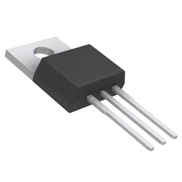
| 描述 | IC REG LDO 5V 0.75A TO220-3低压差稳压器 Single Output LDO 750mA |
| 产品分类 | |
| 品牌 | Texas Instruments |
| 产品手册 | |
| 产品图片 |
|
| rohs | 符合RoHS无铅 / 符合限制有害物质指令(RoHS)规范要求 |
| 产品系列 | 电源管理 IC,低压差稳压器,Texas Instruments TL750M05CKCSE3- |
| 数据手册 | |
| 产品型号 | TL750M05CKCSE3 |
| PCN设计/规格 | |
| 产品目录页面 | |
| 产品种类 | 低压差稳压器 |
| 供应商器件封装 | TO-220-3 |
| 其它名称 | 296-21594-5 |
| 包装 | 管件 |
| 单位重量 | 2 g |
| 商标 | Texas Instruments |
| 回动电压—最大值 | 500 mV at 500 mA |
| 安装类型 | 通孔 |
| 安装风格 | Through Hole |
| 封装 | Tube |
| 封装/外壳 | TO-220-3 |
| 封装/箱体 | TO-220-3 |
| 工作温度 | 0°C ~ 125°C |
| 工厂包装数量 | 50 |
| 最大工作温度 | + 125 C |
| 最大输入电压 | 26 V |
| 最小工作温度 | 0 C |
| 最小输入电压 | + 6 V |
| 标准包装 | 50 |
| 电压-跌落(典型值) | - |
| 电压-输入 | 6 V ~ 26 V |
| 电压-输出 | 5V |
| 电流-输出 | 750mA |
| 电流-限制(最小值) | - |
| 稳压器拓扑 | 正,固定式 |
| 稳压器数 | 1 |
| 系列 | TL750M05 |
| 线路调整率 | 50 mV |
| 负载调节 | 50 mV |
| 输入偏压电流—最大 | 60 mA |
| 输出电压 | 5 V |
| 输出电流 | 750 mA |
| 输出端数量 | 1 Output |
| 输出类型 | Fixed |


- 商务部:美国ITC正式对集成电路等产品启动337调查
- 曝三星4nm工艺存在良率问题 高通将骁龙8 Gen1或转产台积电
- 太阳诱电将投资9.5亿元在常州建新厂生产MLCC 预计2023年完工
- 英特尔发布欧洲新工厂建设计划 深化IDM 2.0 战略
- 台积电先进制程称霸业界 有大客户加持明年业绩稳了
- 达到5530亿美元!SIA预计今年全球半导体销售额将创下新高
- 英特尔拟将自动驾驶子公司Mobileye上市 估值或超500亿美元
- 三星加码芯片和SET,合并消费电子和移动部门,撤换高东真等 CEO
- 三星电子宣布重大人事变动 还合并消费电子和移动部门
- 海关总署:前11个月进口集成电路产品价值2.52万亿元 增长14.8%


PDF Datasheet 数据手册内容提取
TL750M SERIES www.ti.com SLVS021N–JANUARY1988–REVISEDAUGUST2010 LOW-DROPOUT VOLTAGE REGULATORS CheckforSamples:TL750MSERIES FEATURES 1 • LowDropoutVoltage,LessThan0.6Vat750 • OvervoltageProtection mA • InternalThermal-OverloadProtection • LowQuiescentCurrent • InternalOvercurrent-LimitingCircuitry • 60-VLoad-DumpProtection KCS PACKAGE(1) KVU PACKAGE(1) (TOPVIEW) (TOPVIEW) OUTPUT N OUTPUT COMMON O INPUT M COMMON M O INPUT C KTT PACKAGE(1) (TOPVIEW) N OUTPUT O M COMMON M O INPUT C (1)The common terminal is in electrical contact with the mounting base. DESCRIPTION/ORDERING INFORMATION The TL750M series devices are low-dropout positive voltage regulators specifically designed for battery-powered systems. The TL750M devices incorporate onboard overvoltage and current-limiting protection circuitry to protect the devices and the regulated system. The devices are fully protected against 60-V load-dump and reverse-battery conditions. Extremely low quiescent current, even during full-load conditions, makes the TL750M seriesidealforstandbypowersystems. The TL750M offers 5-V, 8-V, 10-V, and 12-V options. The devices are characterized for operation over the virtual junctiontemperaturerange0°Cto125°C. 1 Pleasebeawarethatanimportantnoticeconcerningavailability,standardwarranty,anduseincriticalapplicationsofTexas Instrumentssemiconductorproductsanddisclaimerstheretoappearsattheendofthisdatasheet. PRODUCTIONDATAinformationiscurrentasofpublicationdate. Copyright©1988–2010,TexasInstrumentsIncorporated Products conform to specifications per the terms of the Texas Instruments standard warranty. Production processing does not necessarilyincludetestingofallparameters.
TL750M SERIES SLVS021N–JANUARY1988–REVISEDAUGUST2010 www.ti.com Thesedeviceshavelimitedbuilt-inESDprotection.Theleadsshouldbeshortedtogetherorthedeviceplacedinconductivefoam duringstorageorhandlingtopreventelectrostaticdamagetotheMOSgates. ORDERINGINFORMATION(1) T V TYP PACKAGE(2) ORDERABLE TOP-SIDEMARKING J O PARTNUMBER PowerFLEX™–KVU Reelof3000 TL750M05CKVUR 750M05C 5V TO-220–KCS Tubeof50 TL750M05CKCS TL750M05C TO-263–KTT Reelof500 TL750M05CKTTR TL750M05C TO-220–KCS Tubeof50 TL750M08CKCS TL750M08C 8V 0°Cto125°C PowerFLEX–KVU Reelof3000 TL750M08CKVUR 750M08C TO-220–KCS Tubeof50 TL750M10CKCS TL750M10C 10V PowerFLEX–KVU Reelof3000 TL750M10CKVUR 750M10C TO-220–KCS Tubeof50 TL750M12CKCS TL750M12C 12V PowerFLEX–KVU Reelof3000 TL750M12CKVUR 750M12C (1) Forthemostcurrentpackageandorderinginformation,seethePackageOptionAddendumattheendofthisdocument,orseetheTI websiteatwww.ti.com. (2) Packagedrawings,thermaldata,andsymbolizationareavailableatwww.ti.com/packaging. FUNCTIONALBLOCKDIAGRAM INPUT Current Limiting 28V _ OUTPUT + Bandgap Overvoltage/ Thermal Shutdown COMMON 2 SubmitDocumentationFeedback Copyright©1988–2010,TexasInstrumentsIncorporated
TL750M SERIES www.ti.com SLVS021N–JANUARY1988–REVISEDAUGUST2010 ABSOLUTE MAXIMUM RATINGS(1) overvirtualjunctiontemperaturerange(unlessotherwisenoted) MIN MAX UNIT Continuousinputvoltage 26 V Transientinputvoltage(seeFigure3) 60 V Continuousreverseinputvoltage –15 V Transientreverseinputvoltage t=100ms –50 V KCSpackage 22 q Packagethermalimpedance(2) (3) KTTpackage 25.3 °C/W JA KVUpackage 28 T Virtual-junctiontemperaturerange 0 150 °C J T Storagetemperaturerange –65 150 °C stg (1) Stressesbeyondthoselistedunder"absolutemaximumratings"maycausepermanentdamagetothedevice.Thesearestressratings only,andfunctionaloperationofthedeviceattheseoranyotherconditionsbeyondthoseindicatedunder"recommendedoperating conditions"isnotimplied.Exposuretoabsolute-maximum-ratedconditionsforextendedperiodsmayaffectdevicereliability. (2) MaximumpowerdissipationisafunctionofT(max),q ,andT .Themaximumallowablepowerdissipationatanyallowableambient J JA A temperatureisP =(T(max)–T )/q .OperatingattheabsolutemaximumT of150°Ccanaffectreliability.Duetovariationin D J A JA J individualdeviceelectricalcharacteristicsandthermalresistance,thebuilt-inthermal-overloadprotectionmaybeactivatedatpower levelsslightlyaboveorbelowtherateddissipation. (3) ThepackagethermalimpedanceiscalculatedinaccordancewithJESD51. THERMAL INFORMATION TL750M THERMALMETRIC(1)(2) UNITS KCS(3PINS) KVU(3PINS) KTT(3PINS) q Junction-to-ambientthermalresistance 28.7 50.9 27.5 JA q Junction-to-case(top)thermalresistance 59.8 57.9 43.2 JCtop q Junction-to-boardthermalresistance 0.5 34.8 17.3 JB °C/W y Junction-to-topcharacterizationparameter 5.3 6 2.8 JT y Junction-to-boardcharacterizationparameter 0.4 23.7 9.3 JB q Junction-to-case(bottom)thermalresistance 0.1 0.4 0.3 JCbot (1) Formoreinformationabouttraditionalandnewthermalmetrics,seetheICPackageThermalMetricsapplicationreport,SPRA953. (2) ForthermalestimatesofthisdevicebasedonPCBcopperarea,seetheTIPCBThermalCalculator. RECOMMENDED OPERATING CONDITIONS MIN MAX UNIT TL750M05 6 26 TL750M08 9 26 V Inputvoltage V I TL750M10 11 26 TL750M12 13 26 I Outputcurrent 750 mA O T Operatingvirtual-junctiontemperature 0 125 °C J Copyright©1988–2010,TexasInstrumentsIncorporated SubmitDocumentationFeedback 3
TL750M SERIES SLVS021N–JANUARY1988–REVISEDAUGUST2010 www.ti.com TL750M05 ELECTRICAL CHARACTERISTICS(1) V =14V,I =300mA,T =25°C(unlessotherwisenoted) I O J TL750M05 PARAMETER TESTCONDITIONS UNIT MIN TYP MAX 4.95 5 5.05 Outputvoltage V T =0°Cto125°C 4.9 5.1 J V =9Vto16V,I =250mA 10 25 I O Inputvoltageregulation mV V =6Vto26V,I =250mA 12 50 I O Ripplerejection V =8Vto18V,f=120Hz 50 55 dB I Outputregulationvoltage I =5mAto750mA 20 50 mV O I =500mA 0.5 O Dropoutvoltage V I =750mA 0.6 O Outputnoisevoltage f=10Hzto100kHz 500 mV I =750mA 60 75 O Biascurrent mA I =10mA 5 O (1) Pulse-testingtechniquesmaintainthejunctiontemperatureasclosetotheambienttemperatureaspossible.Thermaleffectsmustbe takenintoaccountseparately.Allcharacteristicsaremeasuredwitha0.1-mFcapacitoracrosstheinputanda10-mFtantalumcapacitor ontheoutput,withequivalentseriesresistancewithintheguidelinesshowninFigure1. TL750M08 ELECTRICAL CHARACTERISTICS(1) V =14V,I =300mA,T =25°C(unlessotherwisenoted) I O J TL750M08 PARAMETER TESTCONDITIONS UNIT MIN TYP MAX 7.92 8 8.08 Outputvoltage V T =0°Cto125°C 7.84 8.16 J V =10Vto17V,I =250mA 12 40 I O Inputvoltageregulation mV V =9Vto26V,I =250mA 15 68 I O Ripplerejection V =11Vto21V,f=120Hz 50 55 dB I Outputregulationvoltage I =5mAto750mA 24 80 mV O I =500mA 0.5 O Dropoutvoltage V I =750mA 0.6 O Outputnoisevoltage f=10Hzto100kHz 500 mV I =750mA 60 75 O Biascurrent mA I =10mA 5 O (1) Pulse-testingtechniquesmaintainthejunctiontemperatureasclosetotheambienttemperatureaspossible.Thermaleffectsmustbe takenintoaccountseparately.Allcharacteristicsaremeasuredwitha0.1-mFcapacitoracrosstheinputanda10-mFtantalumcapacitor ontheoutput,withequivalentseriesresistancewithintheguidelinesshowninFigure1. 4 SubmitDocumentationFeedback Copyright©1988–2010,TexasInstrumentsIncorporated
TL750M SERIES www.ti.com SLVS021N–JANUARY1988–REVISEDAUGUST2010 TL750M10 ELECTRICAL CHARACTERISTICS(1) V =14V,I =300mA,T =25°C(unlessotherwisenoted) I O J TL750M10 PARAMETER TESTCONDITIONS UNIT MIN TYP MAX 9.9 10 10.1 Outputvoltage V T =0°Cto125°C 9.8 10.2 J V =12Vto18V,I =250mA 15 43 I O Inputvoltageregulation mV V =11Vto26V,I =250mA 20 75 I O Ripplerejection V =13Vto23V,f=120Hz 50 55 dB I Outputregulationvoltage I =5mAto750mA 30 100 mV O I =500mA 0.5 O Dropoutvoltage V I =750mA 0.6 O Outputnoisevoltage f=10Hzto100kHz 1000 mV I =750mA 60 75 O Biascurrent mA I =10mA 5 O (1) Pulse-testingtechniquesmaintainthejunctiontemperatureasclosetotheambienttemperatureaspossible.Thermaleffectsmustbe takenintoaccountseparately.Allcharacteristicsaremeasuredwitha0.1-mFcapacitoracrosstheinputanda10-mFtantalumcapacitor ontheoutput,withequivalentseriesresistancewithintheguidelinesshowninFigure1. TL750M12 ELECTRICAL CHARACTERISTICS(1) V =14V,I =300mA,T =25°C(unlessotherwisenoted) I O J TL750M12 PARAMETER TESTCONDITIONS UNIT MIN TYP MAX 11.88 12 12.12 Outputvoltage V T =0°Cto125°C 11.76 12.24 J V =14Vto19V,I =250mA 15 43 I O Inputvoltageregulation mV V =13Vto26V,I =250mA 20 78 I O Ripplerejection V =13Vto23V,f=120Hz 50 55 dB I Outputregulationvoltage I =5mAto750mA 30 120 mV O I =500mA 0.5 O Dropoutvoltage V I =750mA 0.6 O Outputnoisevoltage f=10Hzto100kHz 1000 mV I =750mA 60 75 O Biascurrent mA I =10mA 5 O (1) Pulse-testingtechniquesmaintainthejunctiontemperatureasclosetotheambienttemperatureaspossible.Thermaleffectsmustbe takenintoaccountseparately.Allcharacteristicsaremeasuredwitha0.1-mFcapacitoracrosstheinputanda10-mFtantalumcapacitor ontheoutput,withequivalentseriesresistancewithintheguidelinesshowninFigure1. Copyright©1988–2010,TexasInstrumentsIncorporated SubmitDocumentationFeedback 5
TL750M SERIES SLVS021N–JANUARY1988–REVISEDAUGUST2010 www.ti.com PARAMETER MEASUREMENT INFORMATION The TL750Mxx is a low-dropout regulator. This means that the capacitance loading is important to the performance of the regulator because it is a vital part of the control loop. The capacitor value and the equivalent series resistance (ESR) both affect the control loop and must be defined for the load range and the temperature range. Figure 1 and Figure 2 can establish the capacitance value and ESR range for the best regulator performance. Figure 1 shows the recommended range of ESR for a given load with a 10-mF capacitor on the output. This figurealsoshowsamaximumESRlimitof2Ωandaload-dependentminimumESRlimit. For applications with varying loads, the lightest load condition should be chosen because it is the worst case. Figure 2 shows the relationship of the reciprocal of ESR to the square root of the capacitance with a minimum capacitancelimitof10mFandamaximumESRlimitof2Ω.Thisfigureestablishestheamountthattheminimum ESRlimitshowninFigure1canbeadjustedfordifferentcapacitorvalues. For example, where the minimum load needed is 200 mA, Figure 1 suggests an ESR range of 0.8 Ω to 2 Ω for 10 mF. Figure 2 shows that changing the capacitor from 10 mF to 400 mF can change the ESR minimum by greaterthan3/0.5(or6).Therefore,thenewminimumESRvalueis0.8/6(or0.13Ω ).ThisallowsanESRrange of0.13Ωto2Ω ,achievinganexpandedESRrangebyusingalargercapacitorattheoutput.Forbetterstability in low-current applications, a small resistance placed in series with the capacitor (see Table 1) is recommended, sothatESRsbetterapproximatethoseshowninFigure1andFigure2. Table1.CompensationforIncreasedStabilityatLowCurrents MANUFACTUR ESR PART ADDITIONAL ER CAPACITANCE TYP NUMBER RESISTANCE Applied Load D IL <br/> Current AVX 15mF 0.9Ω TAJB156M010S 1Ω <br/> Load Voltage <br/> KEMET 33mF 0.6Ω T491DA33S6M010 0.5Ω D VL D VL = D IL × ESR <br/> OUTPUTCAPACITOR <br/> EQUIVALENTSERIESRESISTANCE(ESR) STABILITY vs vs LOADCURRENTRANGE EQUIVALENTSERIESRESISTANCE(ESR) 3 0.04 ÎÎ 2.8 CL = 10 m F Not Recommended WR) − 22..64 Cf =I =1 200.1 H m zF TROhepicesor Ramteimognieonnd Nedo tfor 0.035 ÎÎÎÎÎÎÎÎÎÎRPÎÎoecteonmÎÎtimal eÎÎInnsdteaÎÎdb iMlitiÎÎny ESÎÎR ÎÎÏÏ100ÎÎÏÏ0 m FÎÎÏÏ S 2.Î2 ÎÎÎÎÎÎÎÏÎÏÎÏÎÏÎÏÎÏÎÏ 0.03 ÎÎÎÎÎÎÎÎÎÎÏÎÏÎÏ E Region of nce ( Î2 ÎÎÎÎÎÎÎÏÎÏÎÏÎÏÎÏÎÏÎÏ CL 0.025 ÎÎBÎest ÎStabÎilityÎÏÎÏÎÏÎÎÎÎ sta 1.Î8 ÎÎÎÎÎÏÎÏÎÏÏMÎÏÏax EÎÏÏSRÎÏÏ BouÎÏÏndaÎÏry ÎÏ ÎÎÎÎÎÎÏ400ÎÏ m FÎÏÎÎÎÎ esi 1.Î6 ÎÎÎÎÎÏÎÏÎÏÏÎÏÏÎÏÏÎÏÏÎÏÏÎÏÎÏ y − 0.02 ÎÎÎÎÏÎÏÎÏÏÎÏÎÏÎÎÎÎ eries R 11..Î42 ÎÎÎÎÎÏReÎÏgionÎÏ of BÎÏest ÎÏStabÎÏilityÎÏÎÎ Stabilit 0.015 ÎÎÏÎÏÎÏÏ200ÎÏ m FÎÏÎÎÎÎÎÎ nt S Î1 ÎÎÎÎÎÏÎÏÎÏÎÏÎÏÏÏÎÏÏÏÎÏÏÏÎÏÏÎ ÎÎÏ10ÎÏ0 m FÎÏÏÎÏÎÏÎÎÎÎÎÎ ale 0.Î8 ÎÎÎÎÎÎÎÎÎÏÏÎÏÏMin ÎÏÏESRÎÏÏÎ 0.01 ÎÎÏÏÎÏÏÎÏÏÎÎÎÎÎÎÎÎ uiv 0.Î6 ÏÎÏÎÏÎÏÎÏÎÏÎÎÏÎÏÎÏÏÏÎÏÏBouÎÏÏndaÎÏÏry Î ÎÏÎÏÏÏÎÏÏÏÎÏÏÎÎÎÎÎÎÎÎ q E 0.Î4 ÏÎÏÎÏÎÏÎÏÎÏÎÎÏÎÏÎÏÏÎÏÎÏÎÏÎ 0.005 ÎÏÎÏÏÎÏÏ22 mÎÏF ÎÎÎÎÎÎÎÎ Potential Instability Region 0.2 10 m F ÎÏÎÏÎÏÎÏÎÏÎÏÎÎÏÎÏÎÏÎÎÎÎ ÎÏÎÏÏÎÏÏÎÏÎÎÎÎÎÎÎÎ 0 0 0 0.5 1 1.5 2 2.5 3 3.5 4 4.5 5 Î0ÎÎ0Î.1 ÎÎ0.2ÎÎÎ0.3 ÎÎ0.Î4 ÎÎ0.5 ÏÏÏ IL − Load Current Range − A 1/ESR Figure1. Figure2. 6 SubmitDocumentationFeedback Copyright©1988–2010,TexasInstrumentsIncorporated
TL750M SERIES www.ti.com SLVS021N–JANUARY1988–REVISEDAUGUST2010 TYPICAL CHARACTERISTICS Table2.TableofGraphs FIGURE TransientinputvoltagevsTime 3 OutputvoltagevsInputvoltage 4 I =10mA 5 O InputcurrentvsInputvoltage I =100mA 6 O DropoutvoltagevsOutputcurrent 7 QuiescentvoltagevsOutputcurrent 8 Loadtransientresponse 9 Linetransientresponse 10 TRANSIENTINPUTVOLTAGE OUTPUTVOLTAGE vs vs TIME INPUTVOLTAGE 60 14 50 TVfoJI r == t 12≥45 5 °V Cm +s 46e(−t/0.230) 12 ITOJ == 1205 °mCA TL750M12 V − oltage 40 ge − V 10 TL750M10 V a put Volt 8 TL750M08 sient In 30 tr = 1 ms Output 6 an 20 − − Tr VO 4 TL750M05 V I 10 2 0 0 0 100 200 300 400 500 600 0 2 4 6 8 10 12 14 t − Time − ms VI − Input Voltage − V Figure3. Figure4. Copyright©1988–2010,TexasInstrumentsIncorporated SubmitDocumentationFeedback 7
TL750M SERIES SLVS021N–JANUARY1988–REVISEDAUGUST2010 www.ti.com INPUTCURRENT INPUTCURRENT vs vs INPUTVOLTAGE INPUTVOLTAGE 200 350 IO = 10 mA IO = 100 mA 180 TJ = 25°C 300 TJ = 25°C 160 A m 140 A 250 put Current − 112000 ut Current − m 210500 L750M05 L750M08 L750M10 L750M12 n 80 p T T T T − III 60 50M05 50M08 50M10 50M12 − InII 100 40 L7 L7 L7 L7 T T T T 50 20 0 0 0 2 4 6 8 10 12 14 0 2 4 6 8 10 12 14 VI − Input Voltage − V VI − Input Voltage − V Figure5. Figure6. DROPOUTVOLTAGE QUIESCENTCURRENT vs vs OUTPUTCURRENT OUTPUTCURRENT 250 12 TJ = 25°C TJ = 25°C 225 VI = 14 V 10 200 A m V m − − 175 nt 8 e e ag urr Volt 150 nt C 6 ut ce po 125 es Dro Qui 4 100 − Q I 2 75 50 0 0 50 100 150 200 250 300 0 20 40 60 80 100 150 250 350 IO − Output Current − mA IO − Output Current − mA Figure7. Figure8. 8 SubmitDocumentationFeedback Copyright©1988–2010,TexasInstrumentsIncorporated
TL750M SERIES www.ti.com SLVS021N–JANUARY1988–REVISEDAUGUST2010 LOADTRANSIENTRESPONSE LINETRANSIENTRESPONSE mV 200 mV − − VI(NOM) = VO + 1 V ge 100 ge ESR = 2 ut Volta 0 ut VoltamV/DIV ICTLJL = == 2 21050 m° mCAF Outp − 100 Outp20 − VI(NOM) = VO + 1 V − O − 200 ESR = 2 O V V CL = 10 m F nt − mA 115000 TJ = 25°C age − V urre VoltDIV ut C 50 put 1 V/ p n ut 0 − I O − VIN O I 0 50 100 150 200 250 300 350 0 20 40 60 80 100 150 250 350 t − Time − m s t − Time − m s Figure9. Figure10. Copyright©1988–2010,TexasInstrumentsIncorporated SubmitDocumentationFeedback 9
PACKAGE OPTION ADDENDUM www.ti.com 6-Feb-2020 PACKAGING INFORMATION Orderable Device Status Package Type Package Pins Package Eco Plan Lead/Ball Finish MSL Peak Temp Op Temp (°C) Device Marking Samples (1) Drawing Qty (2) (6) (3) (4/5) TL750M05CKCSE3 ACTIVE TO-220 KCS 3 50 Pb-Free SN N / A for Pkg Type 0 to 125 TL750M05C (RoHS) TL750M05CKTTR ACTIVE DDPAK/ KTT 3 500 Green (RoHS SN Level-3-245C-168 HR 0 to 125 TL750M05C TO-263 & no Sb/Br) TL750M05CKVURG3 ACTIVE TO-252 KVU 3 2500 Green (RoHS SN Level-3-260C-168 HR 0 to 125 50M05C & no Sb/Br) TL750M08CKCSE3 ACTIVE TO-220 KCS 3 50 Pb-Free SN N / A for Pkg Type 0 to 125 TL750M08C (RoHS) TL750M08CKVURG3 ACTIVE TO-252 KVU 3 2500 Green (RoHS SN Level-3-260C-168 HR 0 to 125 50M08C & no Sb/Br) TL750M10CKCSE3 ACTIVE TO-220 KCS 3 50 Pb-Free SN N / A for Pkg Type 0 to 125 TL750M10C (RoHS) TL750M10CKVURG3 ACTIVE TO-252 KVU 3 2500 Green (RoHS SN Level-3-260C-168 HR 0 to 125 50M10C & no Sb/Br) TL750M12CKCSE3 ACTIVE TO-220 KCS 3 50 Pb-Free SN N / A for Pkg Type 0 to 125 TL750M12C (RoHS) TL750M12CKVURG3 ACTIVE TO-252 KVU 3 2500 Green (RoHS SN Level-3-260C-168 HR 0 to 125 50M12C & no Sb/Br) (1) The marketing status values are defined as follows: ACTIVE: Product device recommended for new designs. LIFEBUY: TI has announced that the device will be discontinued, and a lifetime-buy period is in effect. NRND: Not recommended for new designs. Device is in production to support existing customers, but TI does not recommend using this part in a new design. PREVIEW: Device has been announced but is not in production. Samples may or may not be available. OBSOLETE: TI has discontinued the production of the device. (2) RoHS: TI defines "RoHS" to mean semiconductor products that are compliant with the current EU RoHS requirements for all 10 RoHS substances, including the requirement that RoHS substance do not exceed 0.1% by weight in homogeneous materials. Where designed to be soldered at high temperatures, "RoHS" products are suitable for use in specified lead-free processes. TI may reference these types of products as "Pb-Free". RoHS Exempt: TI defines "RoHS Exempt" to mean products that contain lead but are compliant with EU RoHS pursuant to a specific EU RoHS exemption. Green: TI defines "Green" to mean the content of Chlorine (Cl) and Bromine (Br) based flame retardants meet JS709B low halogen requirements of <=1000ppm threshold. Antimony trioxide based flame retardants must also meet the <=1000ppm threshold requirement. (3) MSL, Peak Temp. - The Moisture Sensitivity Level rating according to the JEDEC industry standard classifications, and peak solder temperature. Addendum-Page 1
PACKAGE OPTION ADDENDUM www.ti.com 6-Feb-2020 (4) There may be additional marking, which relates to the logo, the lot trace code information, or the environmental category on the device. (5) Multiple Device Markings will be inside parentheses. Only one Device Marking contained in parentheses and separated by a "~" will appear on a device. If a line is indented then it is a continuation of the previous line and the two combined represent the entire Device Marking for that device. (6) Lead/Ball Finish - Orderable Devices may have multiple material finish options. Finish options are separated by a vertical ruled line. Lead/Ball Finish values may wrap to two lines if the finish value exceeds the maximum column width. Important Information and Disclaimer:The information provided on this page represents TI's knowledge and belief as of the date that it is provided. TI bases its knowledge and belief on information provided by third parties, and makes no representation or warranty as to the accuracy of such information. Efforts are underway to better integrate information from third parties. TI has taken and continues to take reasonable steps to provide representative and accurate information but may not have conducted destructive testing or chemical analysis on incoming materials and chemicals. TI and TI suppliers consider certain information to be proprietary, and thus CAS numbers and other limited information may not be available for release. In no event shall TI's liability arising out of such information exceed the total purchase price of the TI part(s) at issue in this document sold by TI to Customer on an annual basis. OTHER QUALIFIED VERSIONS OF TL750M : •Automotive: TL750M-Q1 NOTE: Qualified Version Definitions: •Automotive - Q100 devices qualified for high-reliability automotive applications targeting zero defects Addendum-Page 2
PACKAGE MATERIALS INFORMATION www.ti.com 5-Sep-2014 TAPE AND REEL INFORMATION *Alldimensionsarenominal Device Package Package Pins SPQ Reel Reel A0 B0 K0 P1 W Pin1 Type Drawing Diameter Width (mm) (mm) (mm) (mm) (mm) Quadrant (mm) W1(mm) TL750M05CKTTR DDPAK/ KTT 3 500 330.0 24.4 10.8 16.3 5.11 16.0 24.0 Q2 TO-263 TL750M05CKVURG3 TO-252 KVU 3 2500 330.0 16.4 6.9 10.5 2.7 8.0 16.0 Q2 TL750M08CKVURG3 TO-252 KVU 3 2500 330.0 16.4 6.9 10.5 2.7 8.0 16.0 Q2 TL750M10CKVURG3 TO-252 KVU 3 2500 330.0 16.4 6.9 10.5 2.7 8.0 16.0 Q2 TL750M12CKVURG3 TO-252 KVU 3 2500 330.0 16.4 6.9 10.5 2.7 8.0 16.0 Q2 PackMaterials-Page1
PACKAGE MATERIALS INFORMATION www.ti.com 5-Sep-2014 *Alldimensionsarenominal Device PackageType PackageDrawing Pins SPQ Length(mm) Width(mm) Height(mm) TL750M05CKTTR DDPAK/TO-263 KTT 3 500 340.0 340.0 38.0 TL750M05CKVURG3 TO-252 KVU 3 2500 340.0 340.0 38.0 TL750M08CKVURG3 TO-252 KVU 3 2500 340.0 340.0 38.0 TL750M10CKVURG3 TO-252 KVU 3 2500 340.0 340.0 38.0 TL750M12CKVURG3 TO-252 KVU 3 2500 340.0 340.0 38.0 PackMaterials-Page2
None
PACKAGE OUTLINE KVU0003A TO-252 - 2.52 mm max height SCALE 1.500 TO-252 10.41 9.40 6.22 1.27 B A 5.97 0.89 1 2.29 6.70 2 5.460 6.35 4.58 4.953 3 0.890 3X 1.02 0.635 OPTIONAL NOTE 3 0.61 0.25 C A B 0.61 2.52 MAX C 0.46 0.61 0.46 SEE DETAIL A 5.21 MIN 3 4.32 2 4 MIN 1 EXPOSED 0.51 THERMAL PAD GAGE PLANE NOTE 3 0.13 0 -8 1.78 0.00 1.40 DETA 7.000AIL A TYPICAL 4218915/A 02/2017 NOTES: 1. All linear dimensions are in millimeters. Any dimensions in parenthesis are for reference only. Dimensioning and tolerancing per ASME Y14.5M. 2. This drawing is subject to change without notice. 3. Shape may vary per different assembly sites. 4. Reference JEDEC registration TO-252. www.ti.com
EXAMPLE BOARD LAYOUT KVU0003A TO-252 - 2.52 mm max height TO-252 2X (2.75) (6.15) 2X (1) 1 4 SYMM (4.58) (5.55) 3 (R0.05) TYP (4.2) (2.5) PKG LAND PATTERN EXAMPLE EXPOSED METAL SHOWN SCALE:6X 0.07 MAX 0.07 MIN ALL AROUND ALL AROUND EXPOSED METAL EXPOSED METAL SOLDER MASK METAL METAL UNDER SOLDER MASK OPENING SOLDER MASK OPENING NON SOLDER MASK SOLDER MASK DEFINED DEFINED SOLDER MASK DETAILS NOT TO SCALE 4218915/A 02/2017 NOTES: (continued) 5. This package is designed to be soldered to a thermal pad on the board. For more information, see Texas Instruments literature numbers SLMA002(www.ti.com/lit/slm002) and SLMA004 (www.ti.com/lit/slma004). 6. Vias are optional depending on application, refer to device data sheet. It is recommended that vias under paste be filled, plugged or tented. www.ti.com
EXAMPLE STENCIL DESIGN KVU0003A TO-252 - 2.52 mm max height TO-252 (1.18) TYP 2X (2.75) 2X (1) (0.14) 1 (R0.05) (1.33) TYP SYMM (4.58) 4 3 20X (1.13) (4.2) 20X (0.98) PKG SOLDER PASTE EXAMPLE BASED ON 0.125 mm THICK STENCIL EXPOSED PAD 65% PRINTED SOLDER COVERAGE BY AREA SCALE:8X 4218915/A 02/2017 NOTES: (continued) 7. Laser cutting apertures with trapezoidal walls and rounded corners may offer better paste release. IPC-7525 may have alternate design recommendations. 8. Board assembly site may have different recommendations for stencil design. www.ti.com
None
None
PACKAGE OUTLINE KCS0003B TO-220 - 19.65 mm max height SCALE 0.850 TO-220 4.7 4.4 10.36 1.32 2.9 8.55 9.96 1.22 2.6 8.15 6.5 (6.3) 6.1 ( 3.84) 12.5 12.1 19.65 MAX 9.25 9.05 3X 3.9 MAX 13.12 12.70 1 3 0.90 0.47 3X 0.77 0.34 2.79 2X 2.54 2.59 1.36 3X 1.23 5.08 4222214/B 08/2018 NOTES: 1. Dimensions are in millimeters. Any dimension in brackets or parenthesis are for reference only. Dimensioning and tolerancing per ASME Y14.5M. 2. This drawing is subject to change without notice. 3. Reference JEDEC registration TO-220. www.ti.com
EXAMPLE BOARD LAYOUT KCS0003B TO-220 - 19.65 mm max height TO-220 0.07 MAX 2X (1.7) ALL AROUND 3X (1.2) METAL 2X SOLDER MASK OPENING (1.7) 1 2 3 0.07 MAX R (0.05) ALL AROUND (2.54) SOLDER MASK (5.08) OPENING LAND PATTERN EXAMPLE NON-SOLDER MASK DEFINED SCALE:15X 4222214/B 08/2018 www.ti.com
IMPORTANTNOTICEANDDISCLAIMER TI PROVIDES TECHNICAL AND RELIABILITY DATA (INCLUDING DATASHEETS), DESIGN RESOURCES (INCLUDING REFERENCE DESIGNS), APPLICATION OR OTHER DESIGN ADVICE, WEB TOOLS, SAFETY INFORMATION, AND OTHER RESOURCES “AS IS” AND WITH ALL FAULTS, AND DISCLAIMS ALL WARRANTIES, EXPRESS AND IMPLIED, INCLUDING WITHOUT LIMITATION ANY IMPLIED WARRANTIES OF MERCHANTABILITY, FITNESS FOR A PARTICULAR PURPOSE OR NON-INFRINGEMENT OF THIRD PARTY INTELLECTUAL PROPERTY RIGHTS. These resources are intended for skilled developers designing with TI products. You are solely responsible for (1) selecting the appropriate TI products for your application, (2) designing, validating and testing your application, and (3) ensuring your application meets applicable standards, and any other safety, security, or other requirements. These resources are subject to change without notice. TI grants you permission to use these resources only for development of an application that uses the TI products described in the resource. Other reproduction and display of these resources is prohibited. No license is granted to any other TI intellectual property right or to any third party intellectual property right. TI disclaims responsibility for, and you will fully indemnify TI and its representatives against, any claims, damages, costs, losses, and liabilities arising out of your use of these resources. TI’s products are provided subject to TI’s Terms of Sale (www.ti.com/legal/termsofsale.html) or other applicable terms available either on ti.com or provided in conjunction with such TI products. TI’s provision of these resources does not expand or otherwise alter TI’s applicable warranties or warranty disclaimers for TI products. Mailing Address: Texas Instruments, Post Office Box 655303, Dallas, Texas 75265 Copyright © 2020, Texas Instruments Incorporated