ICGOO在线商城 > 集成电路(IC) > PMIC - 稳压器 - DC DC 切换控制器 > TL5001CD
 Datasheet下载
- 型号: TL5001CD
- 制造商: Texas Instruments
- 库位|库存: xxxx|xxxx
- 要求:
| 数量阶梯 | 香港交货 | 国内含税 |
| +xxxx | $xxxx | ¥xxxx |
查看当月历史价格
查看今年历史价格
TL5001CD产品简介:
ICGOO电子元器件商城为您提供TL5001CD由Texas Instruments设计生产,在icgoo商城现货销售,并且可以通过原厂、代理商等渠道进行代购。 TL5001CD价格参考。Texas InstrumentsTL5001CD封装/规格:PMIC - 稳压器 - DC DC 切换控制器, 降压,升压,反激 稳压器 正 输出 升压,降压,升压/降压 DC-DC 控制器 IC 8-SOIC。您可以下载TL5001CD参考资料、Datasheet数据手册功能说明书,资料中有TL5001CD 详细功能的应用电路图电压和使用方法及教程。
TL5001CD是德州仪器(Texas Instruments)生产的一款PMIC(电源管理集成电路),具体分类为DC-DC切换控制器。这款芯片广泛应用于需要高效、稳定电源转换的场景中,主要用于将输入电压转换为稳定的输出电压,适用于各种工业和消费电子设备。

 应用场景

1. 工业控制系统:
   TL5001CD常用于工业自动化设备中的电源管理系统。例如,在PLC(可编程逻辑控制器)、传感器接口、马达驱动器等设备中,它能够提供稳定的电源输出,确保系统在不同负载条件下正常工作。

2. 通信设备:
   在通信基站、路由器、交换机等网络设备中,TL5001CD可以作为电源管理的核心部件,提供高效的电压转换,保证设备长时间稳定运行。其低功耗和高效率特性有助于减少热量生成,延长设备寿命。

3. 汽车电子:
   汽车电子系统对电源的要求非常严格,TL5001CD可以在车载信息系统、导航系统、娱乐系统等中发挥重要作用。它可以应对车辆启动时的电压波动,确保电子设备的正常工作。

4. 消费电子产品:
   在便携式电子设备如平板电脑、智能手机、智能手表等中,TL5001CD可以用于电池管理和充电电路中,确保电池充电的安全性和稳定性,同时提高电池的使用寿命。

5. 医疗设备:
   医疗设备如监护仪、超声波设备、心电图机等对电源的稳定性和可靠性要求极高。TL5001CD可以为这些设备提供稳定的电源输出,确保设备在关键时刻不会出现故障。

6. 电力供应系统:
   在不间断电源(UPS)和其他电力供应系统中,TL5001CD可以用于主电源和备用电源之间的切换控制,确保在主电源失效时能够迅速切换到备用电源,保障系统的连续运行。

总之,TL5001CD凭借其高效、稳定、低功耗的特点,广泛应用于各类需要可靠电源管理的场景中,特别是在工业、通信、汽车、消费电子和医疗等领域。
| 参数 | 数值 |
| 产品目录 | 集成电路 (IC)半导体 |
| Cuk | 无 |
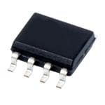
| 描述 | IC REG CTRLR PWM 8SOIC开关控制器 PWM w/wide range |
| 产品分类 | |
| 品牌 | Texas Instruments |
| 产品手册 | |
| 产品图片 |
|
| rohs | 符合RoHS无铅 / 符合限制有害物质指令(RoHS)规范要求 |
| 产品系列 | 电源管理 IC,开关控制器 ,Texas Instruments TL5001CD- |
| 数据手册 | |
| 产品型号 | TL5001CD |
| PWM类型 | 控制器 |
| 产品种类 | 开关控制器 |
| 倍增器 | 无 |
| 其它名称 | 296-26723-5 |
| 分频器 | 无 |
| 包装 | 管件 |
| 升压 | 是 |
| 单位重量 | 72.600 mg |
| 占空比 | 100% |
| 反向 | 无 |
| 反激式 | 是 |
| 商标 | Texas Instruments |
| 安装风格 | SMD/SMT |
| 封装 | Tube |
| 封装/外壳 | 8-SOIC(0.154",3.90mm 宽) |
| 封装/箱体 | SOIC-8 |
| 工作温度 | -20°C ~ 85°C |
| 工厂包装数量 | 75 |
| 最大工作温度 | + 85 C |
| 最小工作温度 | - 20 C |
| 标准包装 | 75 |
| 电压-电源 | 3.6 V ~ 40 V |
| 类型 | Converter |
| 系列 | TL5001 |
| 输入电压 | 3.6 V to 40 V |
| 输出数 | 1 |
| 输出电压 | 51 V |
| 输出电流 | 3 A |
| 输出端数量 | 1 Output |
| 配用 | /product-detail/zh/TL5001EVM-088/296-10208-ND/380455/product-detail/zh/TL5001EVM-089/296-10209-ND/380465/product-detail/zh/TL5001EVM-097/296-10210-ND/380478 |
| 降压 | 是 |
| 隔离式 | 无 |
| 频率-最大值 | 500kHz |


- 商务部:美国ITC正式对集成电路等产品启动337调查
- 曝三星4nm工艺存在良率问题 高通将骁龙8 Gen1或转产台积电
- 太阳诱电将投资9.5亿元在常州建新厂生产MLCC 预计2023年完工
- 英特尔发布欧洲新工厂建设计划 深化IDM 2.0 战略
- 台积电先进制程称霸业界 有大客户加持明年业绩稳了
- 达到5530亿美元!SIA预计今年全球半导体销售额将创下新高
- 英特尔拟将自动驾驶子公司Mobileye上市 估值或超500亿美元
- 三星加码芯片和SET,合并消费电子和移动部门,撤换高东真等 CEO
- 三星电子宣布重大人事变动 还合并消费电子和移动部门
- 海关总署:前11个月进口集成电路产品价值2.52万亿元 增长14.8%


PDF Datasheet 数据手册内容提取
TL5001, TL5001A PULSE-WIDTH-MODULATION CONTROL CIRCUITS SLVS084F – APRIL 1994 – REVISED JANUARY 2002 (cid:0) Complete PWM Power Control D, JG OR P PACKAGE (cid:0) (TOP VIEW) 3.6-V to 40-V Operation (cid:0) Internal Undervoltage-Lockout Circuit OUT 1 8 GND (cid:0) Internal Short-Circuit Protection VCC 2 7 RT (cid:0) Oscillator Frequency...20 kHz to 500 kHz COMP 3 6 DTC (cid:0) FB 4 5 SCP Variable Dead Time Provides Control Over Total Range FK PACKAGE (cid:0) ±3% Tolerance on Reference Voltage (TOP VIEW) (TL5001A) T D C U C N C (cid:0) Available in Q-Temp Automotive N O N G N HighRel Automotive Applications 3 2 1 20 19 Configuration Control / Print Support NC 4 18 NC Qualification to Automotive Standards VCC 5 17 RT description NC 6 16 NC COMP 7 15 DTC The TL5001 and TL5001A incorporate on a single NC 8 14 NC monolithic chip all the functions required for a 9 10 11 12 13 pulse-width-modulation (PWM) control circuit. De- signed primarily for power-supply control, the C B C P C N F N C N TL5001/A contains an error amplifier, a regulator, an S oscillator, a PWM comparator with a dead-time-con- trol input, undervoltage lockout (UVLO), short-circuit protection (SCP), and an open-collector output transistor. The TL5001A has a typical reference voltage tolerance of ±3% compared to ±5% for the TL5001. The error-amplifier common-mode voltage ranges from 0 V to 1.5 V. The noninverting input of the error amplifier is connected to a 1-V reference. Dead-time control (DTC) can be set to provide 0% to 100% dead time by connecting an external resistor between DTC and GND. The oscillator frequency is set by terminating RT with an external resistor to GND. During low V conditions, the UVLO circuit turns the output off until V recovers to its normal CC CC operating range. The TL5001C and TL5001AC are characterized for operation from –20°C to 85°C. The TL5001I and TL5001AI are characterized for operation from –40°C to 85°C. The TL5001Q and TL5001AQ are characterized for operation from –40°C to 125°C. The TL5001M and TL5001AM are characterized for operation from –55°C to 125°C. AVAILABLE OPTIONS PACKAGED DEVICES TA SMALL OUTLINE PLASTIC DIP CERAMIC DIP CHIP CARRIER (D) (P) (JG) (FK) TL5001CD TL5001CP — — –2200°°CC ttoo 8855°°CC TL5001ACD TL5001ACP — — TL5001ID TL5001IP — — –4400°°CC ttoo 8855°°CC TL5001AID TL5001AIP — — TL5001QD — — — –4400°°CC ttoo 112255°°CC TL5001AQD — — — — — TL5001MJG TL5001MFK –5555°°CC ttoo 112255°°CC — — TL5001AMJG TL5001AMFK The D package is available taped and reeled. Add the suffix R to the device type (e.g., TL5001CDR). Please be aware that an important notice concerning availability, standard warranty, and use in critical applications of TexasInstruments semiconductor products and disclaimers thereto appears at the end of this data sheet. PRODUCTION DATA information is current as of publication date. Copyright 2002, Texas Instruments Incorporated Products conform to specifications per the terms of Texas Instruments On products compliant to MIL-PRF-38535, all parameters are tested standard warranty. Production processing does not necessarily include unless otherwise noted. On all other products, production testing of all parameters. processing does not necessarily include testing of all parameters. POST OFFICE BOX 655303 • DALLAS, TEXAS 75265 1
TL5001, TL5001A PULSE-WIDTH-MODULATION CONTROL CIRCUITS SLVS084F – APRIL 1994 – REVISED JANUARY 2002 schematic for typical application VI + TPS1101 VO 2 + VCC 5 1 SCP VO 3 COMP TL5001/A 6 DTC 4 FB 7 RT GND 8 functional block diagram VCC RT DTC OUT 2 7 6 1 UVLO IDT 1 V 2.5 V Reference 1.5 V Voltage 1 V Error SCP OSC PWM/DTC Comparator Amplifier Comparator 1 + 4 FB – 3 COMP SCP Comparator 2 5 SCP 8 GND 2 POST OFFICE BOX 655303 • DALLAS, TEXAS 75265
TL5001, TL5001A PULSE-WIDTH-MODULATION CONTROL CIRCUITS SLVS084F – APRIL 1994 – REVISED JANUARY 2002 detailed description voltage reference A 2.5-V regulator operating from V is used to power the internal circuitry of the TL5001 and TL5001A and as a CC reference for the error amplifier and SCP circuits. A resistive divider provides a 1-V reference for the error amplifier noninverting input which typically is within 2% of nominal over the operating temperature range. error amplifier The error amplifier compares a sample of the dc-to-dc converter output voltage to the 1-V reference and generates an error signal for the PWM comparator. The dc-to-dc converter output voltage is set by selecting the error-amplifier gain (see Figure 1), using the following expression: V = (1 + R1/R2) (1 V) O TL5001/A 3 COMP Compensation Network R1 4 FB VI(FB) – To PWM Comparator R2 + 8 GND Vref = 1 V Figure 1. Error-Amplifier Gain Setting The error-amplifier output is brought out as COMP for use in compensating the dc-to-dc converter control loop for stability. Because the amplifier can only source 45 µA, the total dc load resistance should be 100 kΩ or more. oscillator/PWM The oscillator frequency (f ) can be set between 20 kHz and 500 kHz by connecting a resistor between RT and osc GND. Acceptable resistor values range from 15 kΩ to 250 kΩ. The oscillator frequency can be determined by using the graph shown in Figure 5. The oscillator output is a triangular wave with a minimum value of approximately 0.7 V and a maximum value of approximately 1.3 V. The PWM comparator compares the error-amplifier output voltage and the DTC input voltage to the triangular wave and turns the output transistor off whenever the triangular wave is greater than the lesser of the two inputs. dead-time control (DTC) DTC provides a means of limiting the output-switch duty cycle to a value less than 100%, which is critical for boost and flyback converters. A current source generates a reference current (I ) at DTC that is nominally equal to the DT current at the oscillator timing terminal, RT. Connecting a resistor between DTC and GND generates a dead-time reference voltage (V ), which the PWM/DTC comparator compares to the oscillator triangle wave as described DT in the previous section. Nominally, the maximum duty cycle is 0% when V is 0.7 V or less and 100% when V DT DT is 1.3 V or greater. Because the triangle wave amplitude is a function of frequency and the source impedance of RT is relatively high (1250 Ω), choosing R for a specific maximum duty cycle, D, is accomplished using the DT following equation and the voltage limits for the frequency in question as found in Figure11 (V max and V min osc osc are the maximum and minimum oscillator levels): POST OFFICE BOX 655303 • DALLAS, TEXAS 75265 3
TL5001, TL5001A PULSE-WIDTH-MODULATION CONTROL CIRCUITS SLVS084F – APRIL 1994 – REVISED JANUARY 2002 dead-time control (DTC) (continued) RDT(cid:1)(cid:6)Rt(cid:0)1250(cid:7) (cid:4)D(cid:6)Voscmax – Voscmin(cid:7)(cid:0)Voscmin(cid:5) Where R and R are in ohms, D in decimal DT t Soft start can be implemented by paralleling the DTC resistor with a capacitor (C ) as shown in Figure 2. During DT soft start, the voltage at DTC is derived by the following equation: VDT(cid:2)IDTRDT (cid:6)1–e (cid:6)–t(cid:3)RDTCDT(cid:7)(cid:7) 6 DTC TL5001/A CDT RDT Figure 2. Soft-Start Circuit If the dc-to-dc converter must be in regulation within a specified period of time, the time constant, R C , should DT DT be t /3 to t /5. The TL5001/A remains off until V ≈ 0.7 V, the minimum ramp value. C is discharged every time 0 0 DT DT UVLO or SCP becomes active. undervoltage-lockout (UVLO) protection The undervoltage-lockout circuit turns the output transistor off and resets the SCP latch whenever the supply voltage drops too low (approximately 3 V at 25°C) for proper operation. A hysteresis voltage of 200 mV eliminates false triggering on noise and chattering. short-circuit protection (SCP) The TL5001/A includes short-circuit protection (see Figure 3), which turns the power switch off to prevent damage when the converter output is shorted. When activated, the SCP prevents the switch from being turned on until the internal latching circuit is reset. The circuit is reset by reducing the input voltage until UVLO becomes active or until the SCP terminal is pulled to ground externally. When a short circuit occurs, the error-amplifier output at COMP rises to increase the power-switch duty cycle in an attempt to maintain the output voltage. SCP comparator 1 starts an RC timing circuit when COMP exceeds 1.5 V. If the short is removed and the error-amplifier output drops below 1.5 V before time out, normal converter operation continues. If the fault is still present at the end of the time-out period, the timer sets the latching circuit and turns off the TL5001/A output transistor. 4 POST OFFICE BOX 655303 • DALLAS, TEXAS 75265
TL5001, TL5001A PULSE-WIDTH-MODULATION CONTROL CIRCUITS SLVS084F – APRIL 1994 – REVISED JANUARY 2002 short-circuit protection (SCP) (continued) 2.5 V RSCP 185 kΩ 12 kΩ SCP CSCP Comparator 2 SCP 5 To Output From Error Drive Logic Amp Q1 SCP Vref = 1 V 1.5 V Comparator 1 Q2 Figure 3. SCP Circuit The timer operates by charging an external capacitor (C ), connected between the SCP terminal and ground, SCP towards 2.5 V through a 185-kΩ resistor (R ). The circuit begins charging from an initial voltage of approximately SCP 185mV and times out when the capacitor voltage reaches 1 V. The output of SCP comparator 2 then goes high, turns on Q2, and latches the timer circuit. The expression for setting the SCP time period is derived from the following equation: VSCP(cid:3)(2.5(cid:2)0.185)(cid:5)1(cid:2)e–t(cid:4)(cid:0)(cid:6)(cid:1)0.185 Where τ = R C SCP SCP The end of the time-out period, t , occurs when V = 1 V. Solving for C yields: SCP SCP SCP CSCP(cid:3)12.46(cid:0)tSCP Where t is in seconds, C in µF. t must be much longer (generally 10 to 15 times) than the converter start-up period or the converter will not start. SCP output transistor The output of the TL5001/A is an open-collector transistor with a maximum collector current rating of 21 mA and a voltage rating of 51 V. The output is turned on under the following conditions: the oscillator triangle wave is lower than both the DTC voltage and the error-amplifier output voltage, the UVLO circuit is inactive, and the short-circuit protection circuit is inactive. POST OFFICE BOX 655303 • DALLAS, TEXAS 75265 5
TL5001, TL5001A PULSE-WIDTH-MODULATION CONTROL CIRCUITS SLVS084F – APRIL 1994 – REVISED JANUARY 2002 absolute maximum ratings over operating free-air temperature range (unless otherwise noted)† Supply voltage, V (see Note 1) . . . . . . . . . . . . . . . . . . . . . . . . . . . . . . . . . . . . . . . . . . . . . . . . . . . . . . . . . . . . 41 V CC Amplifier input voltage, V . . . . . . . . . . . . . . . . . . . . . . . . . . . . . . . . . . . . . . . . . . . . . . . . . . . . . . . . . . . . . . . 20 V I(FB) Output voltage, V , OUT . . . . . . . . . . . . . . . . . . . . . . . . . . . . . . . . . . . . . . . . . . . . . . . . . . . . . . . . . . . . . . . . . . . 51 V O Output current, I , OUT . . . . . . . . . . . . . . . . . . . . . . . . . . . . . . . . . . . . . . . . . . . . . . . . . . . . . . . . . . . . . . . . . . 21 mA O Output peak current, I , OUT . . . . . . . . . . . . . . . . . . . . . . . . . . . . . . . . . . . . . . . . . . . . . . . . . . . . . . . 100 mA O(peak) Continuous total power dissipation . . . . . . . . . . . . . . . . . . . . . . . . . . . . . . . . . . . . . . See Dissipation Rating Table Operating ambient temperature range, T : TL5001C, TL5001AC . . . . . . . . . . . . . . . . . . . . . . –20°C to 85°C A TL5001I, TL5001AI . . . . . . . . . . . . . . . . . . . . . . . . –40°C to 85°C TL5001Q, TL5001AQ . . . . . . . . . . . . . . . . . . . . . –40°C to 125°C TL5001M, TL5001AM . . . . . . . . . . . . . . . . . . . . . –55°C to 125°C Storage temperature range, T . . . . . . . . . . . . . . . . . . . . . . . . . . . . . . . . . . . . . . . . . . . . . . . . . . . –65°C to 150°C stg Lead temperature 1,6 mm (1/16 inch) from case for 10 seconds . . . . . . . . . . . . . . . . . . . . . . . . . . . . . . . . 260°C †Stresses beyond those listed under “absolute maximum ratings” may cause permanent damage to the device. These are stress ratings only, and functional operation of the device at these or any other conditions beyond those indicated under “recommended operating conditions” is not implied. Exposure to absolute-maximum-rated conditions for extended periods may affect device reliability. NOTE 1: All voltage values are with respect to network ground terminal. DISSIPATION RATING TABLE TA ≤ 25°C DERATING FACTOR TA = 70°C TA = 85°C TA = 125°C PACKAGE POWER RATING ABOVE TA = 25°C POWER RATING POWER RATING POWER RATING D 725 mW 5.8 mW/°C 464 mW 377 mW 145 mW FK 1375 mW 11.0 mW/°C 880 mW 715 mW 275 mW JG 1050 mW 8.4 mW/°C 672 mW 546 mW 210 mW P 1000 mW 8.0 mW/°C 640 mW 520 mW 200 mW recommended operating conditions MIN MAX UNIT Supply voltage, VCC 3.6 40 V Amplifier input voltage, VI(FB) 0 1.5 V Output voltage, VO, OUT 50 V Output current, IO, OUT 20 mA COMP source current 45 µA COMP dc load resistance 100 kΩ Oscillator timing resistor, Rt 15 250 kΩ Oscillator frequency, fosc 20 500 kHz TL5001C, TL5001AC –20 85 TL5001I, TL5001AI –40 85 OOppeerraattiinngg aammbbiieenntt tteemmppeerraattuurree, TTAA °°CC TL5001Q, TL5001AQ –40 125 TL5001M, TL5001AM –55 125 6 POST OFFICE BOX 655303 • DALLAS, TEXAS 75265
TL5001, TL5001A PULSE-WIDTH-MODULATION CONTROL CIRCUITS SLVS084F – APRIL 1994 – REVISED JANUARY 2002 electrical characteristics over recommended operating free-air temperature range, V = 6 V, CC f = 100 kHz (unless otherwise noted) osc reference TL5001C, TL5001I TL5001AC, TL5001AI PPAARRAAMMEETTEERR TTEESSTT CCOONNDDIITTIIOONNSS UUNNIITT MIN TYP† MAX MIN TYP† MAX Output voltage COMP connected to FB 0.95 1 1.05 0.97 1 1.03 V Input regulation VCC = 3.6 V to 40 V 2 12.5 2 12.5 mV TA = –20°C to 25°C (C suffix) –10 –1 10 –10 –1 10 Output voltage change with temperature TA = –40°C to 25°C (I suffix) –10 –1 10 –10 –1 10 mV/V TA = 25°C to 85°C –10 –2 10 –10 –2 10 †All typical values are at TA = 25°C. undervoltage lockout TL5001C, TL5001I TL5001AC, TL5001AI PPAARRAAMMEETTEERR TTEESSTT CCOONNDDIITTIIOONNSS UUNNIITT MIN TYP† MAX MIN TYP† MAX Upper threshold voltage TA = 25°C 3 3 V Lower threshold voltage TA = 25°C 2.8 2.8 V Hysteresis TA = 25°C 100 200 100 200 mV Reset threshold voltage TA = 25°C 2.1 2.55 2.1 2.55 V †All typical values are at TA = 25°C. short-circuit protection TL5001C, TL5001I TL5001AC, TL5001AI PPAARRAAMMEETTEERR TTEESSTT CCOONNDDIITTIIOONNSS UUNNIITT MIN TYP† MAX MIN TYP† MAX SCP threshold voltage TA = 25°C 0.95 1.00 1.05 0.97 1.00 1.03 V SCP voltage, latched No pullup 140 185 230 140 185 230 mV SCP voltage, UVLO standby No pullup 60 120 60 120 mV Input source current TA = 25°C –10 –15 –20 –10 –15 –20 µA SCP comparator 1 threshold voltage 1.5 1.5 V †All typical values are at TA = 25°C. oscillator TL5001C, TL5001I TL5001AC, TL5001AI PPAARRAAMMEETTEERR TTEESSTT CCOONNDDIITTIIOONNSS UUNNIITT MIN TYP† MAX MIN TYP† MAX Frequency Rt = 100 kΩ 100 100 kHz Standard deviation of frequency 15 15 kHz Frequency change with voltage VCC = 3.6 V to 40 V 1 1 kHz TA = –40°C to 25°C –4 –0.4 4 –4 –0.4 4 kHz Frequency change with temperature TA = –20°C to 25°C –4 –0.4 4 –4 –0.4 4 kHz TA = 25°C to 85°C –4 –0.2 4 –4 –0.2 4 kHz Voltage at RT 1 1 V †All typical values are at TA = 25°C. POST OFFICE BOX 655303 • DALLAS, TEXAS 75265 7
TL5001, TL5001A PULSE-WIDTH-MODULATION CONTROL CIRCUITS SLVS084F – APRIL 1994 – REVISED JANUARY 2002 electrical characteristics over recommended operating free-air temperature range, V = 6 V, CC f = 100 kHz (unless otherwise noted) (continued) osc dead-time control TL5001C, TL5001I TL5001AC, TL5001AI PPAARRAAMMEETTEERR TTEESSTT CCOONNDDIITTIIOONNSS UUNNIITT MIN TYP† MAX MIN TYP† MAX TL5001C V(DT) = 1.5 V 0.9 × IRT‡ 1.1 × IRT 0.9 × IRT‡ 1.1 × IRT OOuuttppuutt ((ssoouurrccee)) ccuurrrreenntt µµAA TL5001I V(DT) = 1.5 V 0.9 × IRT‡ 1.2 × IRT 0.9 × IRT‡ 1.2 × IRT Duty cycle = 0% 0.5 0.7 0.5 0.7 IInnppuutt tthhrreesshhoolldd vvoollttaaggee VV Duty cycle = 100% 1.3 1.5 1.3 1.5 †All typical values are at TA = 25°C. ‡Output source current at RT error amplifier TL5001C, TL5001I TL5001AC, TL5001AI PPAARRAAMMEETTEERR TTEESSTT CCOONNDDIITTIIOONNSS UUNNIITT MIN TYP† MAX MIN TYP† MAX Input voltage VCC = 3.6 V to 40 V 0 1.5 0 1.5 V Input bias current –160 –500 –160 –500 nA Positive 1.5 2.3 1.5 2.3 V OOuuttppuutt vvoollttaaggee sswwiinngg Negative 0.3 0.4 0.3 0.4 V Open-loop voltage amplification 80 80 dB Unity-gain bandwidth 1.5 1.5 MHz Output (sink) current VI(FB) = 1.2 V, COMP = 1 V 100 600 100 600 µA Output (source) current VI(FB) = 0.8 V, COMP = 1 V –45 –70 –45 –70 µA †All typical values are at TA = 25°C. output TL5001C, TL5001I TL5001AC, TL5001AI PPAARRAAMMEETTEERR TTEESSTT CCOONNDDIITTIIOONNSS UUNNIITT MIN TYP† MAX MIN TYP† MAX Output saturation voltage IO = 10 mA 1.5 2 1.5 2 V VO = 50 V, VCC = 0 10 10 OOffff-ssttaattee ccuurrrreenntt µµAA VO = 50 V 10 10 Short-circuit output current VO = 6 V 40 40 mA †All typical values are at TA = 25°C. total device TL5001C, TL5001I TL5001AC, TL5001AI PPAARRAAMMEETTEERR TTEESSTT CCOONNDDIITTIIOONNSS UUNNIITT MIN TYP† MAX MIN TYP† MAX Standby supply current Off state 1 1.5 1 1.5 mA Average supply current Rt = 100 kΩ 1.4 2.1 1.4 2.1 mA †All typical values are at TA = 25°C. 8 POST OFFICE BOX 655303 • DALLAS, TEXAS 75265
TL5001, TL5001A PULSE-WIDTH-MODULATION CONTROL CIRCUITS SLVS084F – APRIL 1994 – REVISED JANUARY 2002 electrical characteristics over recommended operating free-air temperature range, V = 6 V, CC f = 100 kHz (unless otherwise noted) osc reference TL5001Q, TL5001AQ, PARAMETER TEST CONDITIONS TL5001M TL5001AM UNIT MIN TYP† MAX MIN TYP† MAX TA = 25°C 0.95 1.00 1.05 0.97 1.00 1.03 OOuuttppuutt vvoollttaaggee CCOOMMPP ccoonnnneecctteedd ttoo FFBB VV TA = MIN to MAX 0.93 0.98 1.07 0.94 0.98 1.06 Input regulation TA = MIN to MAX VCC = 3.6 V to 40 V 2 12.5 2 12.5 mV Output voltage change with temper- TA = MIN to MAX *–6 2 *6 *–6 2 *6 % ature †All typical values are at TA = 25°C. *Not production tested. undervoltage lockout TL5001Q, TL5001AQ, TL5001M TL5001AM PPAARRAAMMEETTEERR TTEESSTT CCOONNDDIITTIIOONNSS UUNNIITT MIN TYP† MAX MIN TYP† MAX TA = MIN, 25°C 3.00 3.00 UUppppeerr tthhrreesshhoolldd vvoollttaaggee VV TA = MAX 2.55 2.55 TA = MIN, 25°C 2.8 2.8 LLoowweerr tthhrreesshhoolldd vvoollttaaggee VV TA = MAX 2.0 2.0 Hysteresis TA = MIN to MAX 100 200 100 200 mV TA = MIN, 25°C 2.10 2.55 2.10 2.55 RReesseett tthhrreesshhoolldd vvoollttaaggee VV TA = MAX 0.35 0.63 0.35 0.63 †All typical values are at TA = 25°C. short-circuit protection TL5001Q, TL5001AQ, PARAMETER TEST CONDITIONS TL5001M TL5001AM UNIT MIN TYP† MAX MIN TYP† MAX TA = MIN, 25°C 0.95 1.00 1.05 0.97 1.00 1.03 SSCCPP tthhrreesshhoolldd vvoollttaaggee VV TA = MAX 0.93 0.98 1.07 0.94 0.98 1.06 SCP voltage, latched TA = MIN to MAX No pullup 140 185 230 140 185 230 mV SCP voltage, UVLO standby TA = MIN to MAX No pullup 60 120 60 120 mV Equivalent timing resistance TA = MIN to MAX 185 185 kΩ SCP comparator 1 threshold voltage TA = MIN to MAX 1.5 1.5 V †All typical values are at TA = 25°C. POST OFFICE BOX 655303 • DALLAS, TEXAS 75265 9
TL5001, TL5001A PULSE-WIDTH-MODULATION CONTROL CIRCUITS SLVS084F – APRIL 1994 – REVISED JANUARY 2002 electrical characteristics over recommended operating free-air temperature range, V = 6 V, CC f = 100 kHz (unless otherwise noted) (continued) osc oscillator TL5001Q, TL5001AQ, PARAMETER TEST CONDITIONS TL5001M TL5001AM UNIT MIN TYP† MAX MIN TYP† MAX Frequency TA = MIN to MAX Rt = 100 kΩ 100 100 kHz Standard deviation of frequency TA = MIN to MAX 2 2 kHz Frequency change with voltage TA = MIN to MAX VCC = 3.6 V to 40 V 1 1 kHz FFrreeqquueennccyy cchhaannggee wwiitthh Q suffix *–6 3 *6 *–6 3 *6 temperature TTAA == MMIINN ttoo MMAAXX M suffix *–9 5 *9 *–9 5 *9 kkHHzz Voltage at RT TA = MIN to MAX 1 1 V †All typical values are at TA = 25°C. *Not production tested. dead-time control TL5001Q, TL5001M TL5001AQ, TL5001AM PPAARRAAMMEETTEERR TTEESSTT CCOONNDDIITTIIOONNSS UUNNIITT MIN TYP† MAX MIN TYP† MAX Ocuurtrpeuntt (source) TA = MIN to MAX V(DT) = 1.5 V 0.9 × IRT‡ 1.1 × IRT 0.9 × IRT‡ 1.1 × IRT µA Duty cycle = 0% 0.5 0.7 0.5 0.7 TTAA == 2255°°CC Input threshold Duty cycle = 100% 1.3 1.5 1.3 1.5 VV voltage Duty cycle = 0% 0.4 0.7 0.4 0.7 TTAA == MMIINN ttoo MMAAXX Duty cycle = 100% 1.3 1.7 1.3 1.7 †All typical values are at TA = 25°C. ‡Output source current at RT error amplifier TL5001Q, TL5001AQ, TL5001M TL5001AM PPAARRAAMMEETTEERR TTEESSTT CCOONNDDIITTIIOONNSS UUNNIITT MIN TYP† MAX MIN TYP† MAX Input bias current TA = MIN to MAX –160 –500 –160 –500 nA OOuuttpuutt vvoollttaaggee Positive 1.5 2.3 1.5 2.3 V swing Negative TTAA == MMIINN ttoo MMAAXX 0.3 0.4 0.3 0.4 V Open-loop voltage amplification TA = MIN to MAX 80 80 dB Unity-gain bandwidth TA = MIN to MAX 1.5 1.5 MHz Output (sink) current TA = MIN to MAX VI(FB) = 1.2 V, COMP = 1 V 100 600 100 600 µA TA = MIN, 25°C –45 –70 –45 –70 OOuuttppuutt ((ssoouurrccee)) ccuurrrreenntt VVII((FFBB)) == 00.88 VV, CCOOMMPP == 11 VV µµAA TA = MAX –30 –45 –30 –45 †All typical values are at TA = 25°C. 10 POST OFFICE BOX 655303 • DALLAS, TEXAS 75265
TL5001, TL5001A PULSE-WIDTH-MODULATION CONTROL CIRCUITS SLVS084F – APRIL 1994 – REVISED JANUARY 2002 electrical characteristics over recommended operating free-air temperature range, V = 6 V, CC f = 100 kHz (unless otherwise noted) (continued) osc output TL5001Q, TL5001AQ, PARAMETER TEST CONDITIONS TL5001M TL5001AM UNIT MIN TYP† MAX MIN TYP† MAX Output saturation voltage TA = MIN to MAX IO = 10 mA 1.5 2 1.5 2 V VO = 50 V, VCC = 0 10 10 OOffff-ssttaattee ccuurrrreenntt TTAA == MMIINN ttoo MMAAXX µµAA VO = 50 V 10 10 Short-circuit output current TA = MIN to MAX VO = 6 V 40 40 mA †All typical values are at TA = 25°C. total device TL5001Q, TL5001AQ, TL5001M TL5001AM PPAARRAAMMEETTEERR TTEESSTT CCOONNDDIITTIIOONNSS UUNNIITT MIN TYP† MAX MIN TYP† MAX Standby supply current Off state TA = MIN to MAX 1 1.5 1 1.5 mA Average supply current TA = MIN to MAX Rt = 100 kΩ 1.4 2.1 1.4 2.1 mA †All typical values are at TA = 25°C. POST OFFICE BOX 655303 • DALLAS, TEXAS 75265 11
TL5001, TL5001A PULSE-WIDTH-MODULATION CONTROL CIRCUITS SLVS084F – APRIL 1994 – REVISED JANUARY 2002 PARAMETER MEASUREMENT INFORMATION 2.3 V COMP 1.5 V DTC OSC PWM/DTC Comparator OUT SCP Comparator 1 1 V SCP SCP Timing Period SCP 0 V Comparator 2 VCC 3 V NOTE A: The waveforms show timing characteristics for an intermittent short circuit and a longer short circuit that is sufficient to activate SCP. Figure 4. PWM Timing Diagram 12 POST OFFICE BOX 655303 • DALLAS, TEXAS 75265
TL5001, TL5001A PULSE-WIDTH-MODULATION CONTROL CIRCUITS SLVS084F – APRIL 1994 – REVISED JANUARY 2002 TYPICAL CHARACTERISTICS OSCILLATOR FREQUENCY OSCILLATION FREQUENCY vs vs TIMING RESISTANCE AMBIENT TEMPERATURE 1 M 100 VCC = 6 V VCC = 6 V DT Resistance = Rt Rt = 100 kΩ TA = 25°C 98 DT Resistance = 100 kΩ z z H H k ncy – ncy – 96 ue ue q q r Fre 100 k n Fre 94 o o Oscillat Oscillati 92 – f osc f – osc 90 10 k 88 10 k 100 k 1 M – 50 – 25 0 25 50 75 100 Rt – Timing Resistance – Ω TA – Ambient Temperature – °C Figure 5 Figure 6 REFERENCE OUTPUT VOLTAGE REFERENCE OUTPUT VOLTAGE FLUCTUATION vs vs POWER-SUPPLY VOLTAGE AMBIENT TEMPERATURE 2 0.6 1.8 TFAB =a n2d5 °CCOMP n – % ÏVFBCÏ Ca n=Ïd 6 C VOÏMPÏ ÏÏÏÏÏÏÏ – V 1.6 Connected Together atio 0.4 ÏCoÏnneÏctedÏ ToÏgethÏer ÏÏÏÏÏÏ ge ctu Volta 1.4 e Flu 0.2 ÏÏÏÏÏÏÏÏÏÏÏÏÏÏÏÏÏÏÏÏÏÏÏÏ ut 1.2 ag ence Outp 0.18 Output Volt – 0.20 ÏÏÏÏÏÏÏÏÏÏÏÏÏÏÏÏÏÏÏÏÏÏÏÏÏÏÏÏÏÏÏÏÏÏÏÏ er e ef 0.6 c ÏÏÏÏÏÏÏÏÏÏÏÏ R n – 0.4 – ere ÏÏÏÏÏÏÏÏÏÏÏÏ ef 0.4 ef Vr 0.2 – R – 0.6 ÏÏÏÏÏÏÏÏÏÏÏÏ ef ÏÏÏÏÏÏÏÏÏÏÏÏ r V 0 ∆ – 0.8 0 1 2 3 4 5 6 7 8 9 10 – 50 – 25 0 25 50 75 100 VCC – Power-Supply Voltage – V TA – Ambient Temperature – °C Figure 7 Figure 8 POST OFFICE BOX 655303 • DALLAS, TEXAS 75265 13
TL5001, TL5001A PULSE-WIDTH-MODULATION CONTROL CIRCUITS SLVS084F – APRIL 1994 – REVISED JANUARY 2002 TYPICAL CHARACTERISTICS AVERAGE SUPPLY CURRENT AVERAGE SUPPLY CURRENT vs vs POWER-SUPPLY VOLTAGE AMBIENT TEMPERATURE 2 1.3 Rt = 100 kΩ VCC = 6 V TA = 25 °C Rt = 100 kΩ A 1.2 DT Resistance = 100 kΩ m A m ent – 1.5 nt – 1.1 r e ur rr C u pply 1 ply C 1 u p S u ge e S a g 0.9 r a e r v e A 0.5 v – CC – AC 0.8 I C I 0 0 0 10 20 30 40 – 50 – 25 0 25 50 75 100 VCC – Power-Supply Voltage – V TA – Ambient Temperature – °C Figure 9 Figure 10 ERROR AMPLIFIER OUTPUT VOLTAGE PWM TRIANGLE WAVE AMPLITUDE VOLTAGE vs vs OUTPUT (SINK) CURRENT OSCILLATOR FREQUENCY 3 1.8 VCC = 6 V ge – V 1.5 VTAC C= =25 6 ° VC – V 2.5 VTAI( F=B 2) 5= ° 1C.2 V e Volta Voscmax (100% duty cycle) oltage 2 d 1.2 V mplitu utput A O 1.5 Wave 0.9 Voscmin (zero duty cycle) plifier e m 1 gl 0.6 A n r a o Tri Err WM 0.3 – O 0.5 P V 0 0 10 k 100 k 1 M 10 M 0 0.2 0.4 0.6 fosc – Oscillator Frequency – Hz IO – Output (Sink) Current – mA Figure 11 Figure 12 14 POST OFFICE BOX 655303 • DALLAS, TEXAS 75265
TL5001, TL5001A PULSE-WIDTH-MODULATION CONTROL CIRCUITS SLVS084F – APRIL 1994 – REVISED JANUARY 2002 TYPICAL CHARACTERISTICS ERROR AMPLIFIER OUTPUT VOLTAGE ERROR AMPLIFIER OUTPUT VOLTAGE vs vs OUTPUT (SOURCE) CURRENT AMBIENT TEMPERATURE 3 2.46 VCC = 6 V VCC = 6 V VI(FB) = 0.8 V VI(FB) = 0.8 V Voltage – V 2.25 TA = 25 °C Voltage – V 22..4445 No Load Output 1.5 Output 2.43 mplifier 1 mplifier 2.42 A A – Error 0.5 – Error 2.41 O O V V 0 2.40 0 20 40 60 80 100 120 – 50 – 25 0 25 50 75 100 IO – Output (Source) Current – µA TA – Ambient Temperature – °C Figure 13 Figure 14 ERROR AMPLIFIER OPEN-LOOP GAIN AND ERROR AMPLIFIER OUTPUT VOLTAGE PHASE SHIFT vs vs AMBIENT TEMPERATURE FREQUENCY 240 40 –180° VCC = 6 V VCC = 6 V – Error Amplifier Output Voltage – mVO 111228640200000 VNIo(F LBo)a =d 1.2 V – Error Amplifier Open-Loop Gain – dB – 113200000 AφTVA = 25 °C –––––222331470300000°°°°° Error Amplifier Open-Loop Phase Shift V V A 120 – 20 –360° – 50 – 25 0 25 50 75 100 10 k 100 k 1 M 10 M TA – Ambient Temperature – °C f – Frequency – Hz Figure 15 Figure 16 POST OFFICE BOX 655303 • DALLAS, TEXAS 75265 15
TL5001, TL5001A PULSE-WIDTH-MODULATION CONTROL CIRCUITS SLVS084F – APRIL 1994 – REVISED JANUARY 2002 TYPICAL CHARACTERISTICS OUTPUT DUTY CYCLE SCP TIME-OUT PERIOD vs vs DTC VOLTAGE SCP CAPACITANCE 120 12 VCC = 6 V VCC = 6 V Rt = 100 kΩ Rt = 100 kΩ 100 TA = 25 °C s 10 DT Resistance = 200 kΩ m TA = 25 °C % – cle – 80 eriod 8 y P y C Out ut Dut 60 Time- 6 utp 40 CP 4 O S – 20 SCP 2 t 0 0 0 0.5 1 1.5 2 0 20 40 60 80 100 120 DTC Voltage – V CSCP – SCP Capacitance – nF Figure 17 Figure 18 DTC OUTPUT CURRENT OUTPUT SATURATION VOLTAGE vs vs RT OUTPUT CURRENT OUTPUT (SINK) CURRENT – 60 2 DT Voltage = 1.3 V VCC = 6 V TA = 25 °C TA = 25 °C A – 50 µ V nt – ge – 1.5 urre – 40 olta C V ut on Outp – 30 urati 1 C at T S – D – 20 put DT) Out 0.5 IO( – 10 – E C V 0 0 0 – 10 – 20 – 30 – 40 – 50 – 60 0 5 10 15 20 IO – RT Output Current – µA IO – Output (Sink) Current – mA Figure 19 Figure 20 16 POST OFFICE BOX 655303 • DALLAS, TEXAS 75265
TL5001, TL5001A PULSE-WIDTH-MODULATION CONTROL CIRCUITS SLVS084F – APRIL 1994 – REVISED JANUARY 2002 APPLICATION INFORMATION VI 5 V C1 + R1 100 µF 470 Ω 10 V Q1 GND TPS1101 L1 20 µH 3.3 V C3 CR1 0.1 µF MBRS140T3 + 2 C2 100 µF C4 VCC 10 V 1 µF 5 1 + SCP VO GND C5 0.1 µF 3 COMP R7 U1 R5 2.0 kΩ R2 C6 7.50 kΩ 56 kΩ TL5001/A 0.012 µF 1% 6 DTC R4 C7 5.1 kΩ 0.0047 µF R3 4 43 kΩ FB 7 RT GND R6 3.24 kΩ 8 1% Partial Bill of Materials: U1 TL5001/A Texas Instruments Q1 TPS1101 Texas Instruments LI CTX20-1 or Coiltronics 23 turns of #28 wire on Micrometals No. T50-26B core C1 TPSD107M010R0100 AVX C2 TPSD107M010R0100 AVX CR1 MBRS140T3 Motorola NOTES: A. Frequency = 200 kHz B. Duty cycle = 90% max C. Soft-start time constant (TC) = 5.6 ms D. SCP TC = 70 msA Figure 21. Step-Down Converter POST OFFICE BOX 655303 • DALLAS, TEXAS 75265 17
TL5001, TL5001A PULSE-WIDTH-MODULATION CONTROL CIRCUITS SLVS084F – APRIL 1994 – REVISED JANUARY 2002 MECHANICAL DATA D (R-PDSO-G**) PLASTIC SMALL-OUTLINE PACKAGE 14 PIN SHOWN 0.050 (1,27) 0.020 (0,51) 0.010 (0,25) M 0.014 (0,35) 14 8 0.008 (0,20) NOM 0.244 (6,20) 0.228 (5,80) 0.157 (4,00) 0.150 (3,81) Gage Plane 0.010 (0,25) 1 7 0°–8° 0.044 (1,12) A 0.016 (0,40) Seating Plane 0.010 (0,25) 0.004 (0,10) 0.069 (1,75) MAX 0.004 (0,10) PINS ** 8 14 16 DIM 0.197 0.344 0.394 A MAX (5,00) (8,75) (10,00) 0.189 0.337 0.386 A MIN (4,80) (8,55) (9,80) 4040047/D 10/96 NOTES: B. All linear dimensions are in inches (millimeters). C. This drawing is subject to change without notice. D. Body dimensions do not include mold flash or protrusion, not to exceed 0.006 (0,15). E. Falls within JEDEC MS-012 18 POST OFFICE BOX 655303 • DALLAS, TEXAS 75265
TL5001, TL5001A PULSE-WIDTH-MODULATION CONTROL CIRCUITS SLVS084F – APRIL 1994 – REVISED JANUARY 2002 MECHANICAL DATA FK (S-CQCC-N**) LEADLESS CERAMIC CHIP CARRIER 28 TERMINALS SHOWN NO. OF A B 18 17 16 15 14 13 12 TERMINALS MIN MAX MIN MAX ** 0.342 0.358 0.307 0.358 19 11 20 (8,69) (9,09) (7,80) (9,09) 20 10 0.442 0.458 0.406 0.458 28 (11,23) (11,63) (10,31) (11,63) 21 9 B SQ 0.640 0.660 0.495 0.560 44 22 8 (16,26) (16,76) (12,58) (14,22) A SQ 23 7 0.740 0.761 0.495 0.560 52 (18,78) (19,32) (12,58) (14,22) 24 6 0.938 0.962 0.850 0.858 68 (23,83) (24,43) (21,6) (21,8) 25 5 1.141 1.165 1.047 1.063 84 (28,99) (29,59) (26,6) (27,0) 26 27 28 1 2 3 4 0.020 (0,51) 0.080 (2,03) 0.010 (0,25) 0.064 (1,63) 0.020 (0,51) 0.010 (0,25) 0.055 (1,40) 0.045 (1,14) 0.045 (1,14) 0.035 (0,89) 0.028 (0,71) 0.045 (1,14) 0.022 (0,54) 0.035 (0,89) 0.050 (1,27) 4040140/C 11/95 NOTES: A. All linear dimensions are in inches (millimeters). B. This drawing is subject to change without notice. C. This package can be hermetically sealed with a metal lid. D. The terminals are gold-plated. E. Falls within JEDEC MS-004 POST OFFICE BOX 655303 • DALLAS, TEXAS 75265 19
PACKAGE OPTION ADDENDUM www.ti.com 6-Feb-2020 PACKAGING INFORMATION Orderable Device Status Package Type Package Pins Package Eco Plan Lead/Ball Finish MSL Peak Temp Op Temp (°C) Device Marking Samples (1) Drawing Qty (2) (6) (3) (4/5) 5962-9958301QPA ACTIVE CDIP JG 8 1 TBD Call TI N / A for Pkg Type -55 to 125 9958301QPA TL5001M 5962-9958302Q2A ACTIVE LCCC FK 20 1 TBD POST-PLATE N / A for Pkg Type -55 to 125 5962- 9958302Q2A TL5001 AMFKB 5962-9958302QPA ACTIVE CDIP JG 8 1 TBD Call TI N / A for Pkg Type -55 to 125 9958302QPA TL5001AM TL5001ACD ACTIVE SOIC D 8 75 Green (RoHS NIPDAU Level-1-260C-UNLIM -20 to 85 5001AC & no Sb/Br) TL5001ACDR ACTIVE SOIC D 8 2500 Green (RoHS NIPDAU Level-1-260C-UNLIM -20 to 85 5001AC & no Sb/Br) TL5001AID ACTIVE SOIC D 8 75 Green (RoHS NIPDAU Level-1-260C-UNLIM -40 to 85 5001AI & no Sb/Br) TL5001AIDG4 ACTIVE SOIC D 8 75 Green (RoHS NIPDAU Level-1-260C-UNLIM -40 to 85 5001AI & no Sb/Br) TL5001AIDR ACTIVE SOIC D 8 2500 Green (RoHS NIPDAU Level-1-260C-UNLIM -40 to 85 5001AI & no Sb/Br) TL5001AIDRG4 ACTIVE SOIC D 8 2500 Green (RoHS NIPDAU Level-1-260C-UNLIM -40 to 85 5001AI & no Sb/Br) TL5001AIP ACTIVE PDIP P 8 50 Pb-Free NIPDAU N / A for Pkg Type -40 to 85 TL5001AIP (RoHS) TL5001AMFKB ACTIVE LCCC FK 20 1 TBD POST-PLATE N / A for Pkg Type -55 to 125 5962- 9958302Q2A TL5001 AMFKB TL5001AMJGB ACTIVE CDIP JG 8 1 TBD Call TI N / A for Pkg Type -55 to 125 9958302QPA TL5001AM TL5001AQD ACTIVE SOIC D 8 75 Green (RoHS NIPDAU Level-1-260C-UNLIM -40 to 125 5001AQ & no Sb/Br) TL5001AQDG4 ACTIVE SOIC D 8 75 Green (RoHS NIPDAU Level-1-260C-UNLIM 5001AQ & no Sb/Br) TL5001AQDR ACTIVE SOIC D 8 2500 Green (RoHS NIPDAU Level-1-260C-UNLIM -40 to 125 5001AQ & no Sb/Br) Addendum-Page 1
PACKAGE OPTION ADDENDUM www.ti.com 6-Feb-2020 Orderable Device Status Package Type Package Pins Package Eco Plan Lead/Ball Finish MSL Peak Temp Op Temp (°C) Device Marking Samples (1) Drawing Qty (2) (6) (3) (4/5) TL5001AQDRG4 ACTIVE SOIC D 8 2500 Green (RoHS NIPDAU Level-1-260C-UNLIM 5001AQ & no Sb/Br) TL5001CD ACTIVE SOIC D 8 75 Green (RoHS NIPDAU Level-1-260C-UNLIM -25 to 85 5001C & no Sb/Br) TL5001CDG4 ACTIVE SOIC D 8 75 Green (RoHS NIPDAU Level-1-260C-UNLIM -25 to 85 5001C & no Sb/Br) TL5001CDR ACTIVE SOIC D 8 2500 Green (RoHS NIPDAU Level-1-260C-UNLIM -25 to 85 5001C & no Sb/Br) TL5001CDRG4 ACTIVE SOIC D 8 2500 Green (RoHS NIPDAU Level-1-260C-UNLIM -25 to 85 5001C & no Sb/Br) TL5001CP ACTIVE PDIP P 8 50 Pb-Free NIPDAU N / A for Pkg Type -25 to 85 TL5001CP (RoHS) TL5001CPS ACTIVE SO PS 8 80 Green (RoHS NIPDAU Level-1-260C-UNLIM T5001 & no Sb/Br) TL5001CPSR ACTIVE SO PS 8 2000 Green (RoHS NIPDAU Level-1-260C-UNLIM -25 to 85 T5001 & no Sb/Br) TL5001ID ACTIVE SOIC D 8 75 Green (RoHS NIPDAU Level-1-260C-UNLIM -40 to 85 5001I & no Sb/Br) TL5001IDR ACTIVE SOIC D 8 2500 Green (RoHS NIPDAU Level-1-260C-UNLIM -40 to 85 5001I & no Sb/Br) TL5001IDRG4 ACTIVE SOIC D 8 2500 Green (RoHS NIPDAU Level-1-260C-UNLIM -40 to 85 5001I & no Sb/Br) TL5001IP ACTIVE PDIP P 8 50 Pb-Free NIPDAU N / A for Pkg Type -40 to 85 TL5001IP (RoHS) TL5001IPE4 ACTIVE PDIP P 8 50 Pb-Free NIPDAU N / A for Pkg Type -40 to 85 TL5001IP (RoHS) TL5001IPSR ACTIVE SO PS 8 2000 Green (RoHS NIPDAU Level-1-260C-UNLIM Z5001 & no Sb/Br) TL5001MJG ACTIVE CDIP JG 8 1 TBD Call TI N / A for Pkg Type -55 to 125 TL5001MJG TL5001MJGB ACTIVE CDIP JG 8 1 TBD Call TI N / A for Pkg Type -55 to 125 9958301QPA TL5001M TL5001QD ACTIVE SOIC D 8 75 Green (RoHS NIPDAU Level-1-260C-UNLIM -40 to 125 5001Q & no Sb/Br) TL5001QDG4 ACTIVE SOIC D 8 75 Green (RoHS NIPDAU Level-1-260C-UNLIM 5001Q & no Sb/Br) Addendum-Page 2
PACKAGE OPTION ADDENDUM www.ti.com 6-Feb-2020 Orderable Device Status Package Type Package Pins Package Eco Plan Lead/Ball Finish MSL Peak Temp Op Temp (°C) Device Marking Samples (1) Drawing Qty (2) (6) (3) (4/5) TL5001QDR ACTIVE SOIC D 8 2500 Green (RoHS NIPDAU Level-1-260C-UNLIM -40 to 125 5001Q & no Sb/Br) TL5001QDRG4 ACTIVE SOIC D 8 2500 Green (RoHS NIPDAU Level-1-260C-UNLIM 5001Q & no Sb/Br) (1) The marketing status values are defined as follows: ACTIVE: Product device recommended for new designs. LIFEBUY: TI has announced that the device will be discontinued, and a lifetime-buy period is in effect. NRND: Not recommended for new designs. Device is in production to support existing customers, but TI does not recommend using this part in a new design. PREVIEW: Device has been announced but is not in production. Samples may or may not be available. OBSOLETE: TI has discontinued the production of the device. (2) RoHS: TI defines "RoHS" to mean semiconductor products that are compliant with the current EU RoHS requirements for all 10 RoHS substances, including the requirement that RoHS substance do not exceed 0.1% by weight in homogeneous materials. Where designed to be soldered at high temperatures, "RoHS" products are suitable for use in specified lead-free processes. TI may reference these types of products as "Pb-Free". RoHS Exempt: TI defines "RoHS Exempt" to mean products that contain lead but are compliant with EU RoHS pursuant to a specific EU RoHS exemption. Green: TI defines "Green" to mean the content of Chlorine (Cl) and Bromine (Br) based flame retardants meet JS709B low halogen requirements of <=1000ppm threshold. Antimony trioxide based flame retardants must also meet the <=1000ppm threshold requirement. (3) MSL, Peak Temp. - The Moisture Sensitivity Level rating according to the JEDEC industry standard classifications, and peak solder temperature. (4) There may be additional marking, which relates to the logo, the lot trace code information, or the environmental category on the device. (5) Multiple Device Markings will be inside parentheses. Only one Device Marking contained in parentheses and separated by a "~" will appear on a device. If a line is indented then it is a continuation of the previous line and the two combined represent the entire Device Marking for that device. (6) Lead/Ball Finish - Orderable Devices may have multiple material finish options. Finish options are separated by a vertical ruled line. Lead/Ball Finish values may wrap to two lines if the finish value exceeds the maximum column width. Important Information and Disclaimer:The information provided on this page represents TI's knowledge and belief as of the date that it is provided. TI bases its knowledge and belief on information provided by third parties, and makes no representation or warranty as to the accuracy of such information. Efforts are underway to better integrate information from third parties. TI has taken and continues to take reasonable steps to provide representative and accurate information but may not have conducted destructive testing or chemical analysis on incoming materials and chemicals. TI and TI suppliers consider certain information to be proprietary, and thus CAS numbers and other limited information may not be available for release. In no event shall TI's liability arising out of such information exceed the total purchase price of the TI part(s) at issue in this document sold by TI to Customer on an annual basis. OTHER QUALIFIED VERSIONS OF TL5001, TL5001A, TL5001AM, TL5001M : Addendum-Page 3
PACKAGE OPTION ADDENDUM www.ti.com 6-Feb-2020 •Catalog: TL5001A, TL5001 •Automotive: TL5001A-Q1, TL5001A-Q1 •Military: TL5001M, TL5001AM NOTE: Qualified Version Definitions: •Catalog - TI's standard catalog product •Automotive - Q100 devices qualified for high-reliability automotive applications targeting zero defects •Military - QML certified for Military and Defense Applications Addendum-Page 4
PACKAGE MATERIALS INFORMATION www.ti.com 12-Feb-2019 TAPE AND REEL INFORMATION *Alldimensionsarenominal Device Package Package Pins SPQ Reel Reel A0 B0 K0 P1 W Pin1 Type Drawing Diameter Width (mm) (mm) (mm) (mm) (mm) Quadrant (mm) W1(mm) TL5001ACDR SOIC D 8 2500 330.0 12.4 6.4 5.2 2.1 8.0 12.0 Q1 TL5001AIDR SOIC D 8 2500 330.0 12.4 6.4 5.2 2.1 8.0 12.0 Q1 TL5001AQDR SOIC D 8 2500 330.0 12.4 6.4 5.2 2.1 8.0 12.0 Q1 TL5001AQDRG4 SOIC D 8 2500 330.0 12.4 6.4 5.2 2.1 8.0 12.0 Q1 TL5001CDR SOIC D 8 2500 330.0 12.4 6.4 5.2 2.1 8.0 12.0 Q1 TL5001CPSR SO PS 8 2000 330.0 16.4 8.35 6.6 2.5 12.0 16.0 Q1 TL5001IDR SOIC D 8 2500 330.0 12.4 6.4 5.2 2.1 8.0 12.0 Q1 TL5001IPSR SO PS 8 2000 330.0 16.4 8.35 6.6 2.5 12.0 16.0 Q1 TL5001QDR SOIC D 8 2500 330.0 12.4 6.4 5.2 2.1 8.0 12.0 Q1 TL5001QDRG4 SOIC D 8 2500 330.0 12.4 6.4 5.2 2.1 8.0 12.0 Q1 PackMaterials-Page1
PACKAGE MATERIALS INFORMATION www.ti.com 12-Feb-2019 *Alldimensionsarenominal Device PackageType PackageDrawing Pins SPQ Length(mm) Width(mm) Height(mm) TL5001ACDR SOIC D 8 2500 340.5 338.1 20.6 TL5001AIDR SOIC D 8 2500 340.5 338.1 20.6 TL5001AQDR SOIC D 8 2500 350.0 350.0 43.0 TL5001AQDRG4 SOIC D 8 2500 350.0 350.0 43.0 TL5001CDR SOIC D 8 2500 340.5 338.1 20.6 TL5001CPSR SO PS 8 2000 367.0 367.0 38.0 TL5001IDR SOIC D 8 2500 340.5 338.1 20.6 TL5001IPSR SO PS 8 2000 367.0 367.0 38.0 TL5001QDR SOIC D 8 2500 350.0 350.0 43.0 TL5001QDRG4 SOIC D 8 2500 350.0 350.0 43.0 PackMaterials-Page2
None
PACKAGE OUTLINE D0008A SOIC - 1.75 mm max height SCALE 2.800 SMALL OUTLINE INTEGRATED CIRCUIT C SEATING PLANE .228-.244 TYP [5.80-6.19] .004 [0.1] C A PIN 1 ID AREA 6X .050 [1.27] 8 1 2X .189-.197 [4.81-5.00] .150 NOTE 3 [3.81] 4X (0 -15 ) 4 5 8X .012-.020 B .150-.157 [0.31-0.51] .069 MAX [3.81-3.98] .010 [0.25] C A B [1.75] NOTE 4 .005-.010 TYP [0.13-0.25] 4X (0 -15 ) SEE DETAIL A .010 [0.25] .004-.010 0 - 8 [0.11-0.25] .016-.050 [0.41-1.27] DETAIL A (.041) TYPICAL [1.04] 4214825/C 02/2019 NOTES: 1. Linear dimensions are in inches [millimeters]. Dimensions in parenthesis are for reference only. Controlling dimensions are in inches. Dimensioning and tolerancing per ASME Y14.5M. 2. This drawing is subject to change without notice. 3. This dimension does not include mold flash, protrusions, or gate burrs. Mold flash, protrusions, or gate burrs shall not exceed .006 [0.15] per side. 4. This dimension does not include interlead flash. 5. Reference JEDEC registration MS-012, variation AA. www.ti.com
EXAMPLE BOARD LAYOUT D0008A SOIC - 1.75 mm max height SMALL OUTLINE INTEGRATED CIRCUIT 8X (.061 ) [1.55] SYMM SEE DETAILS 1 8 8X (.024) [0.6] SYMM (R.002 ) TYP [0.05] 5 4 6X (.050 ) [1.27] (.213) [5.4] LAND PATTERN EXAMPLE EXPOSED METAL SHOWN SCALE:8X SOLDER MASK SOLDER MASK METAL OPENING OPENING METAL UNDER SOLDER MASK EXPOSED METAL EXPOSED METAL .0028 MAX .0028 MIN [0.07] [0.07] ALL AROUND ALL AROUND NON SOLDER MASK SOLDER MASK DEFINED DEFINED SOLDER MASK DETAILS 4214825/C 02/2019 NOTES: (continued) 6. Publication IPC-7351 may have alternate designs. 7. Solder mask tolerances between and around signal pads can vary based on board fabrication site. www.ti.com
EXAMPLE STENCIL DESIGN D0008A SOIC - 1.75 mm max height SMALL OUTLINE INTEGRATED CIRCUIT 8X (.061 ) [1.55] SYMM 1 8 8X (.024) [0.6] SYMM (R.002 ) TYP [0.05] 5 4 6X (.050 ) [1.27] (.213) [5.4] SOLDER PASTE EXAMPLE BASED ON .005 INCH [0.125 MM] THICK STENCIL SCALE:8X 4214825/C 02/2019 NOTES: (continued) 8. Laser cutting apertures with trapezoidal walls and rounded corners may offer better paste release. IPC-7525 may have alternate design recommendations. 9. Board assembly site may have different recommendations for stencil design. www.ti.com
None
MECHANICAL DATA MCER001A – JANUARY 1995 – REVISED JANUARY 1997 JG (R-GDIP-T8) CERAMIC DUAL-IN-LINE 0.400 (10,16) 0.355 (9,00) 8 5 0.280 (7,11) 0.245 (6,22) 1 4 0.065 (1,65) 0.045 (1,14) 0.063 (1,60) 0.020 (0,51) MIN 0.310 (7,87) 0.015 (0,38) 0.290 (7,37) 0.200 (5,08) MAX Seating Plane 0.130 (3,30) MIN 0.023 (0,58) 0°–15° 0.015 (0,38) 0.100 (2,54) 0.014 (0,36) 0.008 (0,20) 4040107/C 08/96 NOTES: A. All linear dimensions are in inches (millimeters). B. This drawing is subject to change without notice. C. This package can be hermetically sealed with a ceramic lid using glass frit. D. Index point is provided on cap for terminal identification. E. Falls within MIL STD 1835 GDIP1-T8 • POST OFFICE BOX 655303 DALLAS, TEXAS 75265
None
IMPORTANTNOTICEANDDISCLAIMER TI PROVIDES TECHNICAL AND RELIABILITY DATA (INCLUDING DATASHEETS), DESIGN RESOURCES (INCLUDING REFERENCE DESIGNS), APPLICATION OR OTHER DESIGN ADVICE, WEB TOOLS, SAFETY INFORMATION, AND OTHER RESOURCES “AS IS” AND WITH ALL FAULTS, AND DISCLAIMS ALL WARRANTIES, EXPRESS AND IMPLIED, INCLUDING WITHOUT LIMITATION ANY IMPLIED WARRANTIES OF MERCHANTABILITY, FITNESS FOR A PARTICULAR PURPOSE OR NON-INFRINGEMENT OF THIRD PARTY INTELLECTUAL PROPERTY RIGHTS. These resources are intended for skilled developers designing with TI products. You are solely responsible for (1) selecting the appropriate TI products for your application, (2) designing, validating and testing your application, and (3) ensuring your application meets applicable standards, and any other safety, security, or other requirements. These resources are subject to change without notice. TI grants you permission to use these resources only for development of an application that uses the TI products described in the resource. Other reproduction and display of these resources is prohibited. No license is granted to any other TI intellectual property right or to any third party intellectual property right. TI disclaims responsibility for, and you will fully indemnify TI and its representatives against, any claims, damages, costs, losses, and liabilities arising out of your use of these resources. TI’s products are provided subject to TI’s Terms of Sale (www.ti.com/legal/termsofsale.html) or other applicable terms available either on ti.com or provided in conjunction with such TI products. TI’s provision of these resources does not expand or otherwise alter TI’s applicable warranties or warranty disclaimers for TI products. Mailing Address: Texas Instruments, Post Office Box 655303, Dallas, Texas 75265 Copyright © 2020, Texas Instruments Incorporated