ICGOO在线商城 > 集成电路(IC) > 线性 - 放大器 - 仪表,运算放大器,缓冲器放大器 > TL3474AIPWR
 Datasheet下载
- 型号: TL3474AIPWR
- 制造商: Texas Instruments
- 库位|库存: xxxx|xxxx
- 要求:
| 数量阶梯 | 香港交货 | 国内含税 |
| +xxxx | $xxxx | ¥xxxx |
查看当月历史价格
查看今年历史价格
TL3474AIPWR产品简介:
ICGOO电子元器件商城为您提供TL3474AIPWR由Texas Instruments设计生产,在icgoo商城现货销售,并且可以通过原厂、代理商等渠道进行代购。 TL3474AIPWR价格参考。Texas InstrumentsTL3474AIPWR封装/规格:线性 - 放大器 - 仪表,运算放大器,缓冲器放大器, 通用 放大器 4 电路 14-TSSOP。您可以下载TL3474AIPWR参考资料、Datasheet数据手册功能说明书,资料中有TL3474AIPWR 详细功能的应用电路图电压和使用方法及教程。
TL3474AIPWR 是 Texas Instruments(德州仪器)生产的一款低功耗、四路运算放大器,属于线性放大器中的运算放大器类别。它常用于需要中等精度和低功耗的模拟信号处理场合。

其主要应用场景包括:

1. 传感器信号调理:用于放大来自温度、压力、光敏等传感器的微弱模拟信号,提高信号精度和稳定性。

2. 便携式电子设备:由于其低功耗特性,广泛应用于电池供电设备,如手持仪表、数据采集系统和便携式医疗设备。

3. 工业控制系统:用于工业自动化系统中对模拟信号进行放大、滤波和缓冲,提高系统稳定性。

4. 音频处理电路:适用于对音质要求不极端但需多通道放大的音频前置放大电路。

5. 运算与比较电路:可用于构建积分器、微分器、比较器等基础模拟电路,适用于教学实验和通用电子设计。

TL3474AIPWR 采用 14 引脚 TSSOP 封装,具有宽电源电压范围(4V 至 36V),适合多种应用场景,性价比较高,适合中低端模拟电路设计使用。
| 参数 | 数值 |
| -3db带宽 | - |
| 产品目录 | 集成电路 (IC)半导体 |
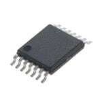
| 描述 | IC OPAMP GP 4MHZ 14TSSOP运算放大器 - 运放 High-Slew-Rate Sngl-Sply Oper Amp |
| 产品分类 | Linear - Amplifiers - Instrumentation, OP Amps, Buffer Amps集成电路 - IC |
| 品牌 | Texas Instruments |
| 产品手册 | http://www.ti.com/litv/slvs461b |
| 产品图片 |
|
| rohs | 符合RoHS无铅 / 符合限制有害物质指令(RoHS)规范要求 |
| 产品系列 | 放大器 IC,运算放大器 - 运放,Texas Instruments TL3474AIPWR- |
| 数据手册 | |
| 产品型号 | TL3474AIPWR |
| 产品种类 | 运算放大器 - 运放 |
| 供应商器件封装 | 14-TSSOP |
| 共模抑制比—最小值 | 80 dB |
| 关闭 | No Shutdown |
| 其它名称 | 296-15117-6 |
| 包装 | Digi-Reel® |
| 单位重量 | 57.200 mg |
| 单电源电压 | 4 V to 36 V |
| 压摆率 | 13 V/µs |
| 双重电源电压 | +/- 3 V, +/- 5 V, +/- 9 V |
| 商标 | Texas Instruments |
| 增益带宽生成 | 4 MHz |
| 增益带宽积 | 4MHz |
| 安装类型 | 表面贴装 |
| 安装风格 | SMD/SMT |
| 封装 | Reel |
| 封装/外壳 | 14-TSSOP(0.173",4.40mm 宽) |
| 封装/箱体 | TSSOP-14 |
| 工作温度 | -40°C ~ 105°C |
| 工作电源电压 | 4 V to 36 V, +/- 2 V to +/- 18 V |
| 工厂包装数量 | 2000 |
| 技术 | Bipolar |
| 放大器类型 | 通用 |
| 最大双重电源电压 | +/- 18 V |
| 最大工作温度 | + 105 C |
| 最小双重电源电压 | +/- 2 V |
| 最小工作温度 | - 40 C |
| 标准包装 | 1 |
| 电压-电源,单/双 (±) | 4 V ~ 36 V, ±2 V ~ 18 V |
| 电压-输入失调 | 1mV |
| 电流-电源 | 3.5mA |
| 电流-输入偏置 | 100nA |
| 电流-输出/通道 | 34mA |
| 电源电流 | 18 mA |
| 电路数 | 4 |
| 系列 | TL3474A |
| 转换速度 | 13 V/us |
| 输入偏压电流—最大 | 500 nA |
| 输入参考电压噪声 | 49 nV |
| 输入补偿电压 | 3 mV |
| 输出类型 | - |
| 通道数量 | 4 Channel |


PDF Datasheet 数据手册内容提取
(cid:1)(cid:2)(cid:3)(cid:4)(cid:5)(cid:4)(cid:6) (cid:1)(cid:2)(cid:3)(cid:4)(cid:5)(cid:4)(cid:7) (cid:8)(cid:9)(cid:10)(cid:8)(cid:11)(cid:12)(cid:2)(cid:13)(cid:14)(cid:11)(cid:15)(cid:7)(cid:1)(cid:13)(cid:6) (cid:12)(cid:9)(cid:16)(cid:10)(cid:2)(cid:13)(cid:11)(cid:12)(cid:17)(cid:18)(cid:18)(cid:2)(cid:19) (cid:20)(cid:18)(cid:13)(cid:15)(cid:7)(cid:1)(cid:9)(cid:20)(cid:16)(cid:7)(cid:2) (cid:7)(cid:21)(cid:18)(cid:2)(cid:9)(cid:22)(cid:9)(cid:13)(cid:15)(cid:12) SLVS461B − JANUARY 2003 − REVISED JULY 2003 (cid:1) Low Offset...3 mV (Max) for A-Grade D, N, OR PW PACKAGE (cid:1) (TOP VIEW) Wide Gain-Bandwidth Product...4 MHz (cid:1) High Slew Rate...13 V/µs 1OUT 1 14 4OUT (cid:1) Fast Settling Time...1.1 µs to 0.1% 1IN− 2 13 4IN− (cid:1) Wide-Range Single-Supply Operation 1IN+ 3 12 4IN+ ...4 V to 36 V VCC+ 4 11 VCC−/GND (cid:1) Wide Input Common-Mode Range Includes 2IN+ 5 10 3IN+ Ground (V ) 2IN− 6 9 3IN− CC− (cid:1) 2OUT 7 8 3OUT Low Total Harmonic Distortion...0.02% (cid:1) Large-Capacitance Drive Capability ...10,000 pF (cid:1) Output Short-Circuit Protection (cid:1) Alternative to MC33074/A and MC34074/A description/ordering information ORDERING INFORMATION TA AVTIO 2m5a°Cx PACKAGE† POARRDT ENRUAMBBLEER MTOAPR-KSIINDGE PDIP (N) Tube of 25 TL3474ACN TL3474ACN Tube of 50 TL3474ACD AA--ggrraaddee:: SSOOIICC ((DD)) TTLL33447744AA Reel of 2500 TL3474ACDR 33 mmVV Tube of 90 TL3474ACPW TTSSSSOOPP ((PPWW)) TT33447744AA Reel of 2000 TL3474ACPWR 00°°CC ttoo 7700°°CC PDIP (N) Tube of 25 TL3474CN TL3474CN Tube of 50 TL3474CD SSttaannddaarrdd ggrraaddee:: SSOOIICC ((DD)) TTLL33447744CC Reel of 2500 TL3474CDR 1100 mmVV Tube of 90 TL3474CPW TTSSSSOOPP ((PPWW)) TTLL33447744 Reel of 2000 TL3474CPWR PDIP (N) Tube of 25 TL3474AIN Z3474A Tube of 50 TL3474AID AA--ggrraaddee:: SSOOIICC ((DD)) TTLL33447744AAII Reel of 2500 TL3474AIDR 33 mmVV Tube of 90 TL3474AIPW TTSSSSOOPP ((PPWW)) ZZ33447744AA Reel of 2000 TL3474AIPWR −−4400°°CC ttoo 110055°°CC PDIP (N) Tube of 25 TL3474IN TL3474IN Tube of 50 TL3474ID SSttaannddaarrdd ggrraaddee:: SSOOIICC ((DD)) TTLL33447744II Reel of 2500 TL3474IDR 1100 mmVV Tube of 90 TL3474IPW TTSSSSOOPP ((PPWW)) ZZ33447744 Reel of 2000 TL3474IPWR †Package drawings, standard packing quantities, thermal data, symbolization, and PCB design guidelines are available at www.ti.com/sc/package. Please be aware that an important notice concerning availability, standard warranty, and use in critical applications of TexasInstruments semiconductor products and disclaimers thereto appears at the end of this data sheet. (cid:18)(cid:15)(cid:20)(cid:23)(cid:17)(cid:24)(cid:1)(cid:9)(cid:20)(cid:16) (cid:23)(cid:7)(cid:1)(cid:7) (cid:25)(cid:26)(cid:27)(cid:28)(cid:29)(cid:30)(cid:31)!(cid:25)(cid:28)(cid:26) (cid:25)" #$(cid:29)(cid:29)%(cid:26)! (cid:31)" (cid:28)(cid:27) &$’((cid:25)#(cid:31)!(cid:25)(cid:28)(cid:26) )(cid:31)!%* Copyright 2003, Texas Instruments Incorporated (cid:18)(cid:29)(cid:28))$#!" #(cid:28)(cid:26)(cid:27)(cid:28)(cid:29)(cid:30) !(cid:28) "&%#(cid:25)(cid:27)(cid:25)#(cid:31)!(cid:25)(cid:28)(cid:26)" &%(cid:29) !+% !%(cid:29)(cid:30)" (cid:28)(cid:27) (cid:1)%,(cid:31)" (cid:9)(cid:26)"!(cid:29)$(cid:30)%(cid:26)!" "!(cid:31)(cid:26))(cid:31)(cid:29)) -(cid:31)(cid:29)(cid:29)(cid:31)(cid:26)!.* (cid:18)(cid:29)(cid:28))$#!(cid:25)(cid:28)(cid:26) &(cid:29)(cid:28)#%""(cid:25)(cid:26)/ )(cid:28)%" (cid:26)(cid:28)! (cid:26)%#%""(cid:31)(cid:29)(cid:25)(. (cid:25)(cid:26)#($)% !%"!(cid:25)(cid:26)/ (cid:28)(cid:27) (cid:31)(( &(cid:31)(cid:29)(cid:31)(cid:30)%!%(cid:29)"* POST OFFICE BOX 655303 • DALLAS, TEXAS 75265 1
(cid:1)(cid:2)(cid:3)(cid:4)(cid:5)(cid:4)(cid:6) (cid:1)(cid:2)(cid:3)(cid:4)(cid:5)(cid:4)(cid:7) (cid:8)(cid:9)(cid:10)(cid:8)(cid:11)(cid:12)(cid:2)(cid:13)(cid:14)(cid:11)(cid:15)(cid:7)(cid:1)(cid:13)(cid:6) (cid:12)(cid:9)(cid:16)(cid:10)(cid:2)(cid:13)(cid:11)(cid:12)(cid:17)(cid:18)(cid:18)(cid:2)(cid:19) (cid:20)(cid:18)(cid:13)(cid:15)(cid:7)(cid:1)(cid:9)(cid:20)(cid:16)(cid:7)(cid:2) (cid:7)(cid:21)(cid:18)(cid:2)(cid:9)(cid:22)(cid:9)(cid:13)(cid:15)(cid:12) SLVS461B − JANUARY 2003 − REVISED JULY 2003 description/ordering information (continued) Quality, low-cost, bipolar fabrication with innovative design concepts is employed for the TL3474, TL3474A operational amplifiers. These devices offer 4 MHz of gain-bandwidth product, 13-V/µs slew rate, and fast settling time without the use of JFET device technology. Although the TL3474 and TL3474A can be operated from split supplies, they are particularly suited for single-supply operation because the common-mode input voltage range includes ground potential (V ). With a Darlington transistor input stage, these devices exhibit high input CC− resistance, low input offset voltage, and high gain. The all-npn output stage, characterized by no dead-band crossover distortion and large output voltage swing, provides high-capacitance drive capability, excellent phase and gain margins, low open-loop high-frequency output impedance, and symmetrical source/sink ac frequency response. These low-cost amplifiers are an alternative to the MC34074/A and MC33074/A operational amplifiers. schematic (each amplifier) VCC+ OUT IN− IN+ VCC−/GND 2 POST OFFICE BOX 655303 • DALLAS, TEXAS 75265
(cid:1)(cid:2)(cid:3)(cid:4)(cid:5)(cid:4)(cid:6) (cid:1)(cid:2)(cid:3)(cid:4)(cid:5)(cid:4)(cid:7) (cid:8)(cid:9)(cid:10)(cid:8)(cid:11)(cid:12)(cid:2)(cid:13)(cid:14)(cid:11)(cid:15)(cid:7)(cid:1)(cid:13)(cid:6) (cid:12)(cid:9)(cid:16)(cid:10)(cid:2)(cid:13)(cid:11)(cid:12)(cid:17)(cid:18)(cid:18)(cid:2)(cid:19) (cid:20)(cid:18)(cid:13)(cid:15)(cid:7)(cid:1)(cid:9)(cid:20)(cid:16)(cid:7)(cid:2) (cid:7)(cid:21)(cid:18)(cid:2)(cid:9)(cid:22)(cid:9)(cid:13)(cid:15)(cid:12) SLVS461B − JANUARY 2003 − REVISED JULY 2003 absolute maximum ratings over operating free-air temperature range (unless otherwise noted)† Supply voltage: V (see Note 1) . . . . . . . . . . . . . . . . . . . . . . . . . . . . . . . . . . . . . . . . . . . . . . . . . . . . . . . . . . . 18 V CC+ V . . . . . . . . . . . . . . . . . . . . . . . . . . . . . . . . . . . . . . . . . . . . . . . . . . . . . . . . . . . . . . . . . . . . . −18 V CC− Differential input voltage, V (see Note 2) . . . . . . . . . . . . . . . . . . . . . . . . . . . . . . . . . . . . . . . . . . . . . . . . . . . ±36 V ID Input voltage, VI (any input) . . . . . . . . . . . . . . . . . . . . . . . . . . . . . . . . . . . . . . . . . . . . . . . . . . . . . . . . . . . . . . . . VCC± Input current, I (each input) . . . . . . . . . . . . . . . . . . . . . . . . . . . . . . . . . . . . . . . . . . . . . . . . . . . . . . . . . . . . . . . ±1 mA I Output current, I . . . . . . . . . . . . . . . . . . . . . . . . . . . . . . . . . . . . . . . . . . . . . . . . . . . . . . . . . . . . . . . . . . . . . . . ±80 mA O Total current into V . . . . . . . . . . . . . . . . . . . . . . . . . . . . . . . . . . . . . . . . . . . . . . . . . . . . . . . . . . . . . . . . . . . 80 mA CC+ Total current out of V . . . . . . . . . . . . . . . . . . . . . . . . . . . . . . . . . . . . . . . . . . . . . . . . . . . . . . . . . . . . . . . . . . 80 mA CC− Duration of short-circuit current at (or below) 25°C (see Note 3) . . . . . . . . . . . . . . . . . . . . . . . . . . . . . . Unlimited Package thermal impedance, θ (see Notes 4 and 5): D package . . . . . . . . . . . . . . . . . . . . . . . . . . . . 86°C/W JA N package . . . . . . . . . . . . . . . . . . . . . . . . . . . . 80°C/W PW package . . . . . . . . . . . . . . . . . . . . . . . . . 113°C/W Operating virtual junction temperature, T . . . . . . . . . . . . . . . . . . . . . . . . . . . . . . . . . . . . . . . . . . . . . . . . . . . 150°C J Lead temperature 1.6 mm (1/16 inch) from case for 10 seconds . . . . . . . . . . . . . . . . . . . . . . . . . . . . . . . 260°C Storage temperature range, T . . . . . . . . . . . . . . . . . . . . . . . . . . . . . . . . . . . . . . . . . . . . . . . . . . . −65°C to 150°C stg †Stresses beyond those listed under “absolute maximum ratings” may cause permanent damage to the device. These are stress ratings only, and functional operation of the device at these or any other conditions beyond those indicated under “recommended operating conditions” is not implied. Exposure to absolute-maximum-rated conditions for extended periods may affect device reliability. NOTES: 1. All voltage values, except differential voltages, are with respect to the midpoint between VCC+ and VCC−/GND. 2. Differential voltages are at the noninverting input with respect to the inverting input. Excessive input current can flow when the input is less than VCC− − 0.3 V. 3. The output can be shorted to either supply. Temperature and/or supply voltages must be limited to ensure that the maximum dissipation rating is not exceeded. θ 4. Maximum power dissipation is a function of TJ(max), JA, and TA. The maximum allowable power dissipation at any allowable ambient temperature is PD = (TJ(max) − TA)/θJA. Operating at the absolute maximum TJ of 150°C can affect reliability. 5. The package thermal impedance is calculated in accordance with JESD 51-7. recommended operating conditions MIN MAX UNIT VCC± Supply voltage 4 36 V VCC = 5 V 0 2.8 VVIICC CCoommmmoonn--mmooddee iinnppuutt vvoollttaaggee VCC± = ±15 V −15 12.8 VV TL3474C, TL3474AC 0 70 TTAA OOppeerraattiinngg ffrreeee--aaiirr tteemmppeerraattuurree °°CC TL3474I, TL3474AI −40 105 POST OFFICE BOX 655303 • DALLAS, TEXAS 75265 3
(cid:1)(cid:2)(cid:3)(cid:4)(cid:5)(cid:4)(cid:6) (cid:1)(cid:2)(cid:3)(cid:4)(cid:5)(cid:4)(cid:7) (cid:8)(cid:9)(cid:10)(cid:8)(cid:11)(cid:12)(cid:2)(cid:13)(cid:14)(cid:11)(cid:15)(cid:7)(cid:1)(cid:13)(cid:6) (cid:12)(cid:9)(cid:16)(cid:10)(cid:2)(cid:13)(cid:11)(cid:12)(cid:17)(cid:18)(cid:18)(cid:2)(cid:19) (cid:20)(cid:18)(cid:13)(cid:15)(cid:7)(cid:1)(cid:9)(cid:20)(cid:16)(cid:7)(cid:2) (cid:7)(cid:21)(cid:18)(cid:2)(cid:9)(cid:22)(cid:9)(cid:13)(cid:15)(cid:12) SLVS461B − JANUARY 2003 − REVISED JULY 2003 electrical characteristics at specified free-air temperature, VCC± = ±15 V (unless otherwise noted) TL3474 TL3474A PPAARRAAMMEETTEERR TTEESSTT CCOONNDDIITTIIOONNSS TTAA MIN TYP† MAX MIN TYP† MAX UUNNIITT VCC = 5 V 25°C 1.5 10 1.5 3 IInnppuutt ooffffsseett VVIIOO vvoollttaaggee VVCCCC == ±±1155 VV Ful2l r5a°nCge‡ 1.0 1102 1.0 35 mmVV Temperature αVIO coefficient of input VIC = 0, VCC = ±15 V Full range‡ 10 10 µV/°C offset voltage VOO = 0, IInnppuutt ooffffsseett RRSS == 5500 ΩΩ 25°C 6 75 6 75 IIIIOO current VVCCCC == ±±1155 VV Full range‡ 300 300 nnAA 25°C 100 500 100 500 IIIIBB IInnppuutt bbiiaass ccuurrrreenntt VVCCCC == ±±1155 VV Full range‡ 700 700 nnAA −15 −15 25°C to to Common-mode 12.8 12.8 VVIICCRR iinnppuutt vvoollttaaggee RRSS == 5500 ΩΩ VV −15 −15 range Full range‡ to to 12.8 12.8 VCC+ = 5 V, VCC− = 0, 25°C 3.7 4 3.7 4 HHiigghh--lleevveell RL = 2 kΩ VVOOHH oouuttppuutt vvoollttaaggee RL = 10 kΩ 25°C 13.6 14 13.6 14 VV RL = 2 kΩ Full range‡ 13.4 13.4 VCC+ = 5 V, VCC− = 0, 25°C 0.1 0.3 0.1 0.3 LLooww--lleevveell RL = 2 kΩ VVOOLL oouuttppuutt vvoollttaaggee RL = 10 kΩ 25°C −14.7 −14.3 −14.7 −14.3 VV RL = 2 kΩ Full range‡ −13.5 −13.5 Large-signal 25°C 25 100 25 100 ddiiffffeerreennttiiaall AAVVDD voltage VVOO == ±±1100 VV,, RRLL == 22 kkΩΩ VV//mmVV Full range‡ 20 20 amplification SShhoorrtt--cciirrccuuiitt Source: VID = 1 V, VO = 0 −10 −34 −10 −34 IIOOSS output current Sink: VID = −1 V, VO = 0 2255°°CC 20 27 20 27 mmAA CCoommmmoonn--mmooddee CCMMRRRR rejection ratio VVIICC == VVIICCRR((mmiinn)),, RRSS == 5500 ΩΩ 2255°°CC 6655 9977 8800 9977 ddBB Supply-voltage kSVR r(e∆jVeCctCio±n/ ∆raVtIioO) VRCSC =± 1 =0 0± 1Ω3.5 V to ±16.5 V, 25°C 70 97 70 97 dB 25°C 3.5 4.5 3.5 4.5 SSuuppppllyy ccuurrrreenntt VVOO == 00,, NNoo llooaadd Full range‡ 4.5 5.5 4.5 5.5 IICCCC ((ppeerr cchhaannnneell)) mmAA VCC+ = 5 V, VO = 2.5 V, 25°C 3.5 4.5 3.5 4.5 VCC− = 0, No load †All typical values are at TA = 25°C. ‡Full range is 0°C to 70°C for the TL3474C, TL3474AC devices and −40°C to 105°C for the TL3474I, TL3474AI devices. 4 POST OFFICE BOX 655303 • DALLAS, TEXAS 75265
(cid:1)(cid:2)(cid:3)(cid:4)(cid:5)(cid:4)(cid:6) (cid:1)(cid:2)(cid:3)(cid:4)(cid:5)(cid:4)(cid:7) (cid:8)(cid:9)(cid:10)(cid:8)(cid:11)(cid:12)(cid:2)(cid:13)(cid:14)(cid:11)(cid:15)(cid:7)(cid:1)(cid:13)(cid:6) (cid:12)(cid:9)(cid:16)(cid:10)(cid:2)(cid:13)(cid:11)(cid:12)(cid:17)(cid:18)(cid:18)(cid:2)(cid:19) (cid:20)(cid:18)(cid:13)(cid:15)(cid:7)(cid:1)(cid:9)(cid:20)(cid:16)(cid:7)(cid:2) (cid:7)(cid:21)(cid:18)(cid:2)(cid:9)(cid:22)(cid:9)(cid:13)(cid:15)(cid:12) SLVS461B − JANUARY 2003 − REVISED JULY 2003 operating characteristics, VCC± = ±15 V, TA = 25°C TL3474 TL3474A PPAARRAAMMEETTEERR TTEESSTT CCOONNDDIITTIIOONNSS UUNNIITT MIN TYP MAX MIN TYP MAX SR+ Positive slew rate VII = −10 V to 10 V, AV = 1 8 10 8 10 RRLL == 22 kkΩΩ,, VV//µss SR− Negative slew rate CL = 300 pF AV = −1 13 13 To 0.1% 1.1 1.1 ttss SSeettttlliinngg ttiimmee AAVVDD == −−11,, 1100--VV sstteepp µss To 0.01% 2.2 2.2 Equivalent input noise Vn voltage f = 1 kHz, RS = 100 Ω 49 49 nV/√Hz Equivalent input noise In current f = 1 kHz 0.22 0.22 pA/√Hz VO(PP) = 2 V to 20 V, RL = 2 kΩ, THD Total harmonic distortion 0.02 0.02 % AVD = 10, f = 10 kHz GBW Gain-bandwidth product f =100 kHz 3 4 3 4 MHz VVOO((PPPP)) == 2200 VV,, RRLL == 22 kkΩΩ,, BBWW PPoowweerr bbaannddwwiiddtthh 116600 116600 kkHHzz AVD = 1, THD = 5.0% RL = 2 kΩ, CL = 0 70 70 φφmm PPhhaassee mmaarrggiinn RL = 2 kΩ, CL = 300 pF 50 50 ddeegg RL = 2 kΩ, CL = 0 12 12 GGaaiinn mmaarrggiinn ddBB RL = 2 kΩ, CL = 300 pF 4 4 Differential input ri resistance VIC = 0 150 150 MΩ Ci Input capacitance VIC = 0 2.5 2.5 pF Channel separation f = 10 kHz 101 101 dB Open-loop output zo impedance f = 1 MHz, AV = 1 20 20 Ω POST OFFICE BOX 655303 • DALLAS, TEXAS 75265 5
(cid:1)(cid:2)(cid:3)(cid:4)(cid:5)(cid:4)(cid:6) (cid:1)(cid:2)(cid:3)(cid:4)(cid:5)(cid:4)(cid:7) (cid:8)(cid:9)(cid:10)(cid:8)(cid:11)(cid:12)(cid:2)(cid:13)(cid:14)(cid:11)(cid:15)(cid:7)(cid:1)(cid:13)(cid:6) (cid:12)(cid:9)(cid:16)(cid:10)(cid:2)(cid:13)(cid:11)(cid:12)(cid:17)(cid:18)(cid:18)(cid:2)(cid:19) (cid:20)(cid:18)(cid:13)(cid:15)(cid:7)(cid:1)(cid:9)(cid:20)(cid:16)(cid:7)(cid:2) (cid:7)(cid:21)(cid:18)(cid:2)(cid:9)(cid:22)(cid:9)(cid:13)(cid:15)(cid:12) SLVS461B − JANUARY 2003 − REVISED JULY 2003 TYPICAL CHARACTERISTICS (TA = 25°C UNLESS OTHERWISE NOTED) OUTPUT IMPEDANCE TOTAL HARMONIC DISTORTION vs vs FREQUENCY FREQUENCY 80 0.6 VCC± = ±15 V VCC± = ±15 V 70 VCM = 0 V VO = 2 Vpp ∆VIOO == 0± 0V.5 mA 0.5 RL = 2 k 60 AV = 1000 0.4 Ω 50 % − − e D nc 40 TH 0.3 a d pe 30 AV = 1000 m I 0.2 20 AV = 100 AV = 100 10 AV = 10 AV = 1 0.1 AV = 10 AV = 1 0 0 1 k 10 k 100 k 1 M 10 M 10 100 1 k 10 k 100 k Frequency − Hz Frequency − Hz Figure 1 Figure 2 GAIN AND PHASE NORMALIZED INPUT BIAS CURRENT vs vs FREQUENCY TEMPERATURE 35 0 1.6 VCC± = ±15 V 30 Phase 0 pF VCM = 0 Phase 300 pF −50 d) 1.4 25 e z ali 20 m −100 r 1.2 n − dB 1105 VCC± = ±15 V −150 se − Deg rrent (No 1 Gai 5 VRoL == 02 Vk Pha s Cu a −200 Bi 0.8 0 ut p −5 Gain 0 pF −250 In 0.6 −10 Gain 300 pF −15 −300 0.4 100 K 1 M 10 M −55 −40 0 25 70 85 125 Frequency − Hz TA − Temperature − °C Figure 3 Figure 4 6 POST OFFICE BOX 655303 • DALLAS, TEXAS 75265
(cid:1)(cid:2)(cid:3)(cid:4)(cid:5)(cid:4)(cid:6) (cid:1)(cid:2)(cid:3)(cid:4)(cid:5)(cid:4)(cid:7) (cid:8)(cid:9)(cid:10)(cid:8)(cid:11)(cid:12)(cid:2)(cid:13)(cid:14)(cid:11)(cid:15)(cid:7)(cid:1)(cid:13)(cid:6) (cid:12)(cid:9)(cid:16)(cid:10)(cid:2)(cid:13)(cid:11)(cid:12)(cid:17)(cid:18)(cid:18)(cid:2)(cid:19) (cid:20)(cid:18)(cid:13)(cid:15)(cid:7)(cid:1)(cid:9)(cid:20)(cid:16)(cid:7)(cid:2) (cid:7)(cid:21)(cid:18)(cid:2)(cid:9)(cid:22)(cid:9)(cid:13)(cid:15)(cid:12) SLVS461B − JANUARY 2003 − REVISED JULY 2003 TYPICAL CHARACTERISTICS (TA = 25°C UNLESS OTHERWISE NOTED) OFFSET VOLTAGE DRIFT SUPPLY CURRENT vs vs TEMPERATURE SUPPLY VOLTAGE 20 2.0 1.9 VCC± = ±15 V 18 TA = −55°C 1.8 VCM = 0 V 1.7 16 1.6 1.5 A m 14 V 1.4 − m 1.3 rrent 12 set − 11..12 Cu 10 Off 1.0 upply 8 TA = 25°C V − IO 000...789 S − 6 TA = 125°C 0.6 C 0.5 C 4 0.4 I 0.3 2 0.2 0.1 0 0.0 4 9 14 19 24 29 34 −55 −25 0 25 50 75 100 125 VCC − Supply Voltage − V TA − Temperature − °C Figure 5 Figure 6 NORMALIZED INPUT BIAS CURRENT NORMALIZED SLEW RATE vs vs INPUT COMMON-MODE VOLTAGE TEMPERATURE 1.4 1.5 VCC± = ±15 V VCC± = ±15 V d) 1.4 AV = 1 e RL = 2 k z mali 1.2 d) 1.3 CL = 500 pF ent (Nor ormalize 11..12 Curr 1 e (N s at 1 a R Bi w nput 0.8 Sle 0.9 − I 0.8 B I I 0.7 0.6 0.6 −14 −10 −6 −2 2 6 10 14 −55 −25 0 25 50 75 100 125 VIC − Input Common-Mode Voltage − V TA − Temperature − °C Figure 7 Figure 8 POST OFFICE BOX 655303 • DALLAS, TEXAS 75265 7
(cid:1)(cid:2)(cid:3)(cid:4)(cid:5)(cid:4)(cid:6) (cid:1)(cid:2)(cid:3)(cid:4)(cid:5)(cid:4)(cid:7) (cid:8)(cid:9)(cid:10)(cid:8)(cid:11)(cid:12)(cid:2)(cid:13)(cid:14)(cid:11)(cid:15)(cid:7)(cid:1)(cid:13)(cid:6) (cid:12)(cid:9)(cid:16)(cid:10)(cid:2)(cid:13)(cid:11)(cid:12)(cid:17)(cid:18)(cid:18)(cid:2)(cid:19) (cid:20)(cid:18)(cid:13)(cid:15)(cid:7)(cid:1)(cid:9)(cid:20)(cid:16)(cid:7)(cid:2) (cid:7)(cid:21)(cid:18)(cid:2)(cid:9)(cid:22)(cid:9)(cid:13)(cid:15)(cid:12) SLVS461B − JANUARY 2003 − REVISED JULY 2003 TYPICAL CHARACTERISTICS (TA = 25°C UNLESS OTHERWISE NOTED) COMMON-MODE REJECTION vs FREQUENCY 120 25°C VCC± = ±15 V VCM = 0 V ∆VCM = ±15 V 100 125°C −55°C 80 B d − R 60 R M C 40 20 55°C 25°C 125°C 0 10 100 1 k 10 k 100 k 1 M 10 M Frequency − Hz Figure 9 8 POST OFFICE BOX 655303 • DALLAS, TEXAS 75265
PACKAGE OPTION ADDENDUM www.ti.com 6-Feb-2020 PACKAGING INFORMATION Orderable Device Status Package Type Package Pins Package Eco Plan Lead/Ball Finish MSL Peak Temp Op Temp (°C) Device Marking Samples (1) Drawing Qty (2) (6) (3) (4/5) TL3474ACD ACTIVE SOIC D 14 50 Green (RoHS NIPDAU Level-1-260C-UNLIM 0 to 70 TL3474A & no Sb/Br) TL3474ACDR ACTIVE SOIC D 14 2500 Green (RoHS NIPDAU Level-1-260C-UNLIM 0 to 70 TL3474A & no Sb/Br) TL3474ACN ACTIVE PDIP N 14 25 Green (RoHS NIPDAU N / A for Pkg Type 0 to 70 TL3474ACN & no Sb/Br) TL3474ACPW ACTIVE TSSOP PW 14 90 Green (RoHS NIPDAU Level-1-260C-UNLIM 0 to 70 T3474A & no Sb/Br) TL3474ACPWR ACTIVE TSSOP PW 14 2000 Green (RoHS NIPDAU Level-1-260C-UNLIM 0 to 70 T3474A & no Sb/Br) TL3474AID ACTIVE SOIC D 14 50 Green (RoHS NIPDAU Level-1-260C-UNLIM -40 to 105 TL3474AI & no Sb/Br) TL3474AIDR ACTIVE SOIC D 14 2500 Green (RoHS NIPDAU Level-1-260C-UNLIM -40 to 105 TL3474AI & no Sb/Br) TL3474AIDRE4 ACTIVE SOIC D 14 2500 Green (RoHS NIPDAU Level-1-260C-UNLIM -40 to 105 TL3474AI & no Sb/Br) TL3474AIN ACTIVE PDIP N 14 25 Green (RoHS NIPDAU N / A for Pkg Type -40 to 105 TL3474AIN & no Sb/Br) TL3474AIPW ACTIVE TSSOP PW 14 90 Green (RoHS NIPDAU Level-1-260C-UNLIM -40 to 105 Z3474A & no Sb/Br) TL3474AIPWE4 ACTIVE TSSOP PW 14 90 Green (RoHS NIPDAU Level-1-260C-UNLIM -40 to 105 Z3474A & no Sb/Br) TL3474AIPWR ACTIVE TSSOP PW 14 2000 Green (RoHS NIPDAU Level-1-260C-UNLIM -40 to 105 Z3474A & no Sb/Br) TL3474CD ACTIVE SOIC D 14 50 Green (RoHS NIPDAU Level-1-260C-UNLIM 0 to 70 TL3474C & no Sb/Br) TL3474CDR ACTIVE SOIC D 14 2500 Green (RoHS NIPDAU Level-1-260C-UNLIM 0 to 70 TL3474C & no Sb/Br) TL3474CN ACTIVE PDIP N 14 25 Green (RoHS NIPDAU N / A for Pkg Type 0 to 70 TL3474CN & no Sb/Br) TL3474CPW ACTIVE TSSOP PW 14 90 Green (RoHS NIPDAU Level-1-260C-UNLIM 0 to 70 T3474 & no Sb/Br) TL3474CPWR ACTIVE TSSOP PW 14 2000 Green (RoHS NIPDAU Level-1-260C-UNLIM 0 to 70 T3474 & no Sb/Br) Addendum-Page 1
PACKAGE OPTION ADDENDUM www.ti.com 6-Feb-2020 Orderable Device Status Package Type Package Pins Package Eco Plan Lead/Ball Finish MSL Peak Temp Op Temp (°C) Device Marking Samples (1) Drawing Qty (2) (6) (3) (4/5) TL3474ID ACTIVE SOIC D 14 50 Green (RoHS NIPDAU Level-1-260C-UNLIM -40 to 105 TL3474I & no Sb/Br) TL3474IDR ACTIVE SOIC D 14 2500 Green (RoHS NIPDAU Level-1-260C-UNLIM -40 to 105 TL3474I & no Sb/Br) TL3474IN ACTIVE PDIP N 14 25 Green (RoHS NIPDAU N / A for Pkg Type -40 to 105 TL3474IN & no Sb/Br) TL3474IPW ACTIVE TSSOP PW 14 90 Green (RoHS NIPDAU Level-1-260C-UNLIM -40 to 105 Z3474 & no Sb/Br) TL3474IPWR ACTIVE TSSOP PW 14 2000 Green (RoHS NIPDAU Level-1-260C-UNLIM -40 to 105 Z3474 & no Sb/Br) (1) The marketing status values are defined as follows: ACTIVE: Product device recommended for new designs. LIFEBUY: TI has announced that the device will be discontinued, and a lifetime-buy period is in effect. NRND: Not recommended for new designs. Device is in production to support existing customers, but TI does not recommend using this part in a new design. PREVIEW: Device has been announced but is not in production. Samples may or may not be available. OBSOLETE: TI has discontinued the production of the device. (2) RoHS: TI defines "RoHS" to mean semiconductor products that are compliant with the current EU RoHS requirements for all 10 RoHS substances, including the requirement that RoHS substance do not exceed 0.1% by weight in homogeneous materials. Where designed to be soldered at high temperatures, "RoHS" products are suitable for use in specified lead-free processes. TI may reference these types of products as "Pb-Free". RoHS Exempt: TI defines "RoHS Exempt" to mean products that contain lead but are compliant with EU RoHS pursuant to a specific EU RoHS exemption. Green: TI defines "Green" to mean the content of Chlorine (Cl) and Bromine (Br) based flame retardants meet JS709B low halogen requirements of <=1000ppm threshold. Antimony trioxide based flame retardants must also meet the <=1000ppm threshold requirement. (3) MSL, Peak Temp. - The Moisture Sensitivity Level rating according to the JEDEC industry standard classifications, and peak solder temperature. (4) There may be additional marking, which relates to the logo, the lot trace code information, or the environmental category on the device. (5) Multiple Device Markings will be inside parentheses. Only one Device Marking contained in parentheses and separated by a "~" will appear on a device. If a line is indented then it is a continuation of the previous line and the two combined represent the entire Device Marking for that device. (6) Lead/Ball Finish - Orderable Devices may have multiple material finish options. Finish options are separated by a vertical ruled line. Lead/Ball Finish values may wrap to two lines if the finish value exceeds the maximum column width. Important Information and Disclaimer:The information provided on this page represents TI's knowledge and belief as of the date that it is provided. TI bases its knowledge and belief on information provided by third parties, and makes no representation or warranty as to the accuracy of such information. Efforts are underway to better integrate information from third parties. TI has taken and Addendum-Page 2
PACKAGE OPTION ADDENDUM www.ti.com 6-Feb-2020 continues to take reasonable steps to provide representative and accurate information but may not have conducted destructive testing or chemical analysis on incoming materials and chemicals. TI and TI suppliers consider certain information to be proprietary, and thus CAS numbers and other limited information may not be available for release. In no event shall TI's liability arising out of such information exceed the total purchase price of the TI part(s) at issue in this document sold by TI to Customer on an annual basis. Addendum-Page 3
PACKAGE MATERIALS INFORMATION www.ti.com 14-Jul-2012 TAPE AND REEL INFORMATION *Alldimensionsarenominal Device Package Package Pins SPQ Reel Reel A0 B0 K0 P1 W Pin1 Type Drawing Diameter Width (mm) (mm) (mm) (mm) (mm) Quadrant (mm) W1(mm) TL3474ACDR SOIC D 14 2500 330.0 16.4 6.5 9.0 2.1 8.0 16.0 Q1 TL3474ACPWR TSSOP PW 14 2000 330.0 12.4 6.9 5.6 1.6 8.0 12.0 Q1 TL3474AIDR SOIC D 14 2500 330.0 16.4 6.5 9.0 2.1 8.0 16.0 Q1 TL3474AIPWR TSSOP PW 14 2000 330.0 12.4 6.9 5.6 1.6 8.0 12.0 Q1 TL3474CDR SOIC D 14 2500 330.0 16.4 6.5 9.0 2.1 8.0 16.0 Q1 TL3474CPWR TSSOP PW 14 2000 330.0 12.4 6.9 5.6 1.6 8.0 12.0 Q1 TL3474IDR SOIC D 14 2500 330.0 16.4 6.5 9.0 2.1 8.0 16.0 Q1 TL3474IPWR TSSOP PW 14 2000 330.0 12.4 6.9 5.6 1.6 8.0 12.0 Q1 PackMaterials-Page1
PACKAGE MATERIALS INFORMATION www.ti.com 14-Jul-2012 *Alldimensionsarenominal Device PackageType PackageDrawing Pins SPQ Length(mm) Width(mm) Height(mm) TL3474ACDR SOIC D 14 2500 333.2 345.9 28.6 TL3474ACPWR TSSOP PW 14 2000 367.0 367.0 35.0 TL3474AIDR SOIC D 14 2500 333.2 345.9 28.6 TL3474AIPWR TSSOP PW 14 2000 367.0 367.0 35.0 TL3474CDR SOIC D 14 2500 333.2 345.9 28.6 TL3474CPWR TSSOP PW 14 2000 367.0 367.0 35.0 TL3474IDR SOIC D 14 2500 333.2 345.9 28.6 TL3474IPWR TSSOP PW 14 2000 367.0 367.0 35.0 PackMaterials-Page2
None
None
None
None
None
IMPORTANTNOTICEANDDISCLAIMER TI PROVIDES TECHNICAL AND RELIABILITY DATA (INCLUDING DATASHEETS), DESIGN RESOURCES (INCLUDING REFERENCE DESIGNS), APPLICATION OR OTHER DESIGN ADVICE, WEB TOOLS, SAFETY INFORMATION, AND OTHER RESOURCES “AS IS” AND WITH ALL FAULTS, AND DISCLAIMS ALL WARRANTIES, EXPRESS AND IMPLIED, INCLUDING WITHOUT LIMITATION ANY IMPLIED WARRANTIES OF MERCHANTABILITY, FITNESS FOR A PARTICULAR PURPOSE OR NON-INFRINGEMENT OF THIRD PARTY INTELLECTUAL PROPERTY RIGHTS. These resources are intended for skilled developers designing with TI products. You are solely responsible for (1) selecting the appropriate TI products for your application, (2) designing, validating and testing your application, and (3) ensuring your application meets applicable standards, and any other safety, security, or other requirements. These resources are subject to change without notice. TI grants you permission to use these resources only for development of an application that uses the TI products described in the resource. Other reproduction and display of these resources is prohibited. No license is granted to any other TI intellectual property right or to any third party intellectual property right. TI disclaims responsibility for, and you will fully indemnify TI and its representatives against, any claims, damages, costs, losses, and liabilities arising out of your use of these resources. TI’s products are provided subject to TI’s Terms of Sale (www.ti.com/legal/termsofsale.html) or other applicable terms available either on ti.com or provided in conjunction with such TI products. TI’s provision of these resources does not expand or otherwise alter TI’s applicable warranties or warranty disclaimers for TI products. Mailing Address: Texas Instruments, Post Office Box 655303, Dallas, Texas 75265 Copyright © 2020, Texas Instruments Incorporated