ICGOO在线商城 > 集成电路(IC) > 线性 - 放大器 - 仪表,运算放大器,缓冲器放大器 > TL3414AIPWR
 Datasheet下载
- 型号: TL3414AIPWR
- 制造商: Texas Instruments
- 库位|库存: xxxx|xxxx
- 要求:
| 数量阶梯 | 香港交货 | 国内含税 |
| +xxxx | $xxxx | ¥xxxx |
查看当月历史价格
查看今年历史价格
TL3414AIPWR产品简介:
ICGOO电子元器件商城为您提供TL3414AIPWR由Texas Instruments设计生产,在icgoo商城现货销售,并且可以通过原厂、代理商等渠道进行代购。 TL3414AIPWR价格参考¥0.54-¥1.02。Texas InstrumentsTL3414AIPWR封装/规格:线性 - 放大器 - 仪表,运算放大器,缓冲器放大器, 通用 放大器 2 电路 8-TSSOP。您可以下载TL3414AIPWR参考资料、Datasheet数据手册功能说明书,资料中有TL3414AIPWR 详细功能的应用电路图电压和使用方法及教程。
TL3414AIPWR 是由 Texas Instruments(德州仪器)生产的一款线性放大器,属于仪表、运算放大器和缓冲器放大器类别。该型号具有高精度、低功耗和宽工作电压范围的特点,适用于多种工业和消费类应用场景。以下是其主要应用场景:

 1. 工业自动化与控制
   - TL3414AIPWR 可用于工业控制系统中的信号调理电路。例如,在传感器信号的放大和转换中,它能够提供高精度和稳定的输出。
   - 在数据采集系统中,作为前置放大器,用于放大微弱的模拟信号,同时减少噪声干扰。

 2. 医疗设备
   - 在医疗电子领域,如心电图(ECG)、血压监测仪等设备中,TL3414AIPWR 可以用作信号放大器,确保生物电信号的准确采集和处理。
   - 其低功耗特性适合便携式医疗设备,延长电池使用寿命。

 3. 音频处理
   - 该放大器可用于音频信号的预处理阶段,例如麦克风信号的放大或滤波。
   - 在低功耗音频设备中,如便携式音响或耳机放大器,TL3414AIPWR 能够提供高质量的音频信号输出。

 4. 汽车电子
   - 在汽车传感器系统中,如温度、压力或加速度传感器,TL3414AIPWR 可以对传感器输出的微弱信号进行放大和处理。
   - 其宽工作电压范围(±5V 至 ±18V)使其适应汽车环境中的电源波动。

 5. 通信设备
   - 在通信领域,该放大器可用于信号调节和放大,特别是在低噪声要求的应用中。
   - 例如,无线模块中的信号链路部分,需要高增益和低失真的放大功能。

 6. 消费电子产品
   - TL3414AIPWR 可用于家用电器中的控制电路,如洗衣机、空调的传感器信号处理。
   - 在智能家居设备中,作为信号放大器,支持精确的环境监测(如温湿度传感器)。

 总结
TL3414AIPWR 凭借其高精度、低功耗和稳定性,广泛应用于工业、医疗、汽车、通信和消费电子等领域。其具体应用场景取决于系统的信号处理需求,特别适合需要高精度放大和低噪声性能的场合。
| 参数 | 数值 |
| -3db带宽 | - |
| 产品目录 | 集成电路 (IC)半导体 |
| 描述 | IC OPAMP GP 2MHZ 8TSSOP运算放大器 - 运放 Dual Hi Output Current Op Amp |
| 产品分类 | Linear - Amplifiers - Instrumentation, OP Amps, Buffer Amps集成电路 - IC |
| 品牌 | Texas Instruments |
| 产品手册 | |
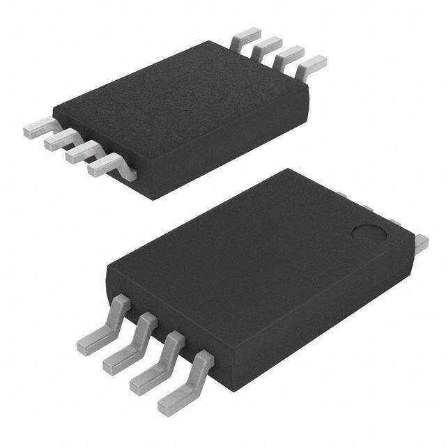
| 产品图片 |
|
| rohs | 符合RoHS无铅 / 符合限制有害物质指令(RoHS)规范要求 |
| 产品系列 | 放大器 IC,运算放大器 - 运放,Texas Instruments TL3414AIPWR- |
| 数据手册 | |
| 产品型号 | TL3414AIPWR |
| 产品种类 | 运算放大器 - 运放 |
| 供应商器件封装 | 8-TSSOP |
| 共模抑制比—最小值 | 70 dB |
| 关闭 | No Shutdown |
| 其它名称 | 296-17543-6 |
| 包装 | Digi-Reel® |
| 单位重量 | 39 mg |
| 单电源电压 | 3 V to 15 V |
| 压摆率 | 1.3 V/µs |
| 双重电源电压 | +/- 3 V, +/- 5 V |
| 商标 | Texas Instruments |
| 增益带宽生成 | 1.1 MHz |
| 增益带宽积 | 2MHz |
| 安装类型 | 表面贴装 |
| 安装风格 | SMD/SMT |
| 封装 | Reel |
| 封装/外壳 | 8-TSSOP(0.173",4.40mm 宽) |
| 封装/箱体 | TSSOP-8 |
| 工作温度 | -40°C ~ 85°C |
| 工作电源电压 | 3 V to 15 V, +/- 1.5 V to +/- 7.5 V |
| 工厂包装数量 | 2000 |
| 技术 | Bipolar |
| 放大器类型 | 通用 |
| 最大双重电源电压 | +/- 7.5 V |
| 最大工作温度 | + 85 C |
| 最小双重电源电压 | +/- 1.5 V |
| 最小工作温度 | - 40 C |
| 标准包装 | 1 |
| 电压-电源,单/双 (±) | 3 V ~ 15 V, ±1.5 V ~ 7.5 V |
| 电压-输入失调 | 2mV |
| 电流-电源 | 4mA |
| 电流-输入偏置 | 300nA |
| 电流-输出/通道 | - |
| 电源电流 | 6 mA |
| 电路数 | 2 |
| 系列 | TL3414A |
| 转换速度 | 0.83 V/us |
| 输入偏压电流—最大 | 600 nA |
| 输入参考电压噪声 | 18 nV |
| 输入补偿电压 | 5 mV |
| 输出类型 | - |
| 通道数量 | 2 Channel |


- 商务部:美国ITC正式对集成电路等产品启动337调查
- 曝三星4nm工艺存在良率问题 高通将骁龙8 Gen1或转产台积电
- 太阳诱电将投资9.5亿元在常州建新厂生产MLCC 预计2023年完工
- 英特尔发布欧洲新工厂建设计划 深化IDM 2.0 战略
- 台积电先进制程称霸业界 有大客户加持明年业绩稳了
- 达到5530亿美元!SIA预计今年全球半导体销售额将创下新高
- 英特尔拟将自动驾驶子公司Mobileye上市 估值或超500亿美元
- 三星加码芯片和SET,合并消费电子和移动部门,撤换高东真等 CEO
- 三星电子宣布重大人事变动 还合并消费电子和移动部门
- 海关总署:前11个月进口集成电路产品价值2.52万亿元 增长14.8%


PDF Datasheet 数据手册内容提取
(cid:1)(cid:2)(cid:3)(cid:4)(cid:5)(cid:4)(cid:6) (cid:7)(cid:8)(cid:6)(cid:2) (cid:9)(cid:10)(cid:11)(cid:9)(cid:12)(cid:13)(cid:8)(cid:1)(cid:14)(cid:8)(cid:1)(cid:12)(cid:15)(cid:8)(cid:16)(cid:16)(cid:17)(cid:18)(cid:1) (cid:13)(cid:14)(cid:17)(cid:16)(cid:6)(cid:1)(cid:10)(cid:13)(cid:18)(cid:6)(cid:2) (cid:6)(cid:19)(cid:14)(cid:2)(cid:10)(cid:20)(cid:10)(cid:17)(cid:16) SLOS453A − DECEMBER 2004 − REVISED JANUARY 2005 (cid:1) Single/Dual Power-Supply Operation D (SOIC), P (PDIP), OR PW (TSSOP) PACKAGE (cid:1) (TOP VIEW) High Output Current...70 mA, V = 5 V CC+ (cid:1) Wide Operating Voltage... 3 V to 15 V OUT1 1 8 VCC+ (Single Supply) IN1− 2 7 OUT2 (cid:1) Ideal for Headphone Drivers IN1+ 3 6 IN2− VCC− 4 5 IN2+ description/ordering information The TL3414A device is a dual operational amplifier that can be operated with single or dual power supplies. In addition to high gain and high output voltage swing, it is capable of driving a 70-mA load, making it ideally suited for simple, low-cost audio-amplifier applications, such as headphone amplifiers in DVD and CDRW applications. ORDERING INFORMATION ORDERABLE TOP-SIDE TA PACKAGE† PART NUMBER MARKING PDIP (P) Tube of 50 TL3414AIP TL3414AIP Tube of 75 TL3414AID SSOOIICC ((DD)) ZZ33441144AA −−4400°CC ttoo 8855°CC Reel of 2500 TL3414AIDR Tube of 150 TL3414AIPW TTSSSSOOPP ((PPWW)) ZZ33441144AA Reel of 2000 TL3414AIPWR †Package drawings, standard packing quantities, thermal data, symbolization, and PCB design guidelines are available at www.ti.com/sc/package. symbol (each amplifier) IN+ + OUT IN− − Please be aware that an important notice concerning availability, standard warranty, and use in critical applications of TexasInstruments semiconductor products and disclaimers thereto appears at the end of this data sheet. (cid:14)(cid:16)(cid:13)(cid:7)(cid:8)(cid:15)(cid:1)(cid:10)(cid:13)(cid:18) (cid:7)(cid:6)(cid:1)(cid:6) (cid:21)(cid:22)(cid:23)(cid:24)(cid:25)(cid:26)(cid:27)(cid:28)(cid:21)(cid:24)(cid:22) (cid:21)(cid:29) (cid:30)(cid:31)(cid:25)(cid:25)!(cid:22)(cid:28) (cid:27)(cid:29) (cid:24)(cid:23) "(cid:31)#$(cid:21)(cid:30)(cid:27)(cid:28)(cid:21)(cid:24)(cid:22) %(cid:27)(cid:28)!& Copyright 2005, Texas Instruments Incorporated (cid:14)(cid:25)(cid:24)%(cid:31)(cid:30)(cid:28)(cid:29) (cid:30)(cid:24)(cid:22)(cid:23)(cid:24)(cid:25)(cid:26) (cid:28)(cid:24) (cid:29)"!(cid:30)(cid:21)(cid:23)(cid:21)(cid:30)(cid:27)(cid:28)(cid:21)(cid:24)(cid:22)(cid:29) "!(cid:25) (cid:28)’! (cid:28)!(cid:25)(cid:26)(cid:29) (cid:24)(cid:23) (cid:1)!((cid:27)(cid:29) (cid:10)(cid:22)(cid:29)(cid:28)(cid:25)(cid:31)(cid:26)!(cid:22)(cid:28)(cid:29) (cid:29)(cid:28)(cid:27)(cid:22)%(cid:27)(cid:25)% )(cid:27)(cid:25)(cid:25)(cid:27)(cid:22)(cid:28)*& (cid:14)(cid:25)(cid:24)%(cid:31)(cid:30)(cid:28)(cid:21)(cid:24)(cid:22) "(cid:25)(cid:24)(cid:30)!(cid:29)(cid:29)(cid:21)(cid:22)+ %(cid:24)!(cid:29) (cid:22)(cid:24)(cid:28) (cid:22)!(cid:30)!(cid:29)(cid:29)(cid:27)(cid:25)(cid:21)$* (cid:21)(cid:22)(cid:30)$(cid:31)%! (cid:28)!(cid:29)(cid:28)(cid:21)(cid:22)+ (cid:24)(cid:23) (cid:27)$$ "(cid:27)(cid:25)(cid:27)(cid:26)!(cid:28)!(cid:25)(cid:29)& POST OFFICE BOX 655303 • DALLAS, TEXAS 75265 1
(cid:1)(cid:2)(cid:3)(cid:4)(cid:5)(cid:4)(cid:6) (cid:7)(cid:8)(cid:6)(cid:2) (cid:9)(cid:10)(cid:11)(cid:9)(cid:12)(cid:13)(cid:8)(cid:1)(cid:14)(cid:8)(cid:1)(cid:12)(cid:15)(cid:8)(cid:16)(cid:16)(cid:17)(cid:18)(cid:1) (cid:13)(cid:14)(cid:17)(cid:16)(cid:6)(cid:1)(cid:10)(cid:13)(cid:18)(cid:6)(cid:2) (cid:6)(cid:19)(cid:14)(cid:2)(cid:10)(cid:20)(cid:10)(cid:17)(cid:16) SLOS453A − DECEMBER 2004 − REVISED JANUARY 2005 simplified schematic V+ R Input− R Input+ V− Output absolute maximum ratings over operating free-air temperature range (unless otherwise noted)† Supply voltage, V (single supply) . . . . . . . . . . . . . . . . . . . . . . . . . . . . . . . . . . . . . . . . . . . . . . . . . . . . . . . . . 15 V CC+ Supply voltage, V (single supply) . . . . . . . . . . . . . . . . . . . . . . . . . . . . . . . . . . . . . . . . . . . . . . . . . . . . . . . . . . 0 V CC− Supply voltage, V (dual supply) . . . . . . . . . . . . . . . . . . . . . . . . . . . . . . . . . . . . . . . . . . . . . . . . . . . . . . . . . 7.5 V CC+ Supply voltage, V (dual supply) . . . . . . . . . . . . . . . . . . . . . . . . . . . . . . . . . . . . . . . . . . . . . . . . . . . . . . . . −7.5 V CC− Supply voltage, (V to V ) . . . . . . . . . . . . . . . . . . . . . . . . . . . . . . . . . . . . . . . . . . . . . . . . . . . . . . . . . . . . . 15 V CC− CC+ Input voltage, either input (see Note 1) . . . . . . . . . . . . . . . . . . . . . . . . . . . . . . . . . . . . . . . . . . . . . . . V or V CC− CC+ Input current (see Note 2) . . . . . . . . . . . . . . . . . . . . . . . . . . . . . . . . . . . . . . . . . . . . . . . . . . . . . . . . . . . . . . . . ±10 mA Duration of output short circuit (see Note 3) . . . . . . . . . . . . . . . . . . . . . . . . . . . . . . . . . . . . . . . . . . . . . . . Unlimited Package thermal impedance, θ (see Notes 4 and 5): D package . . . . . . . . . . . . . . . . . . . . . . . . . . . . 97°C/W JA P package . . . . . . . . . . . . . . . . . . . . . . . . . . . . 85°C/W PW package . . . . . . . . . . . . . . . . . . . . . . . . . 149°C/W Operating virtual junction temperature, T . . . . . . . . . . . . . . . . . . . . . . . . . . . . . . . . . . . . . . . . . . . . . . . . . . . 150°C J Storage temperature range, T . . . . . . . . . . . . . . . . . . . . . . . . . . . . . . . . . . . . . . . . . . . . . . . . . . . −40°C to 125°C stg †Stresses beyond those listed under “absolute maximum ratings” may cause permanent damage to the device. These are stress ratings only, and functional operation of the device at these or any other conditions beyond those indicated under “recommended operating conditions” is not implied. Exposure to absolute-maximum-rated conditions for extended periods may affect device reliability. NOTES: 1. The magnitude of the input voltage must never exceed the magnitude of the supply voltage. 2. Excessive input current will flow if a differential input voltage in excess of approximately 0.6 V is applied between the inputs, unless some limiting resistance is used. 3. The output may be shorted to ground or either power supply. Temperature and/or supply voltages must be limited to ensure the maximum dissipation rating is not exceeded. 4. Maximum power dissipation is a function of TJ(max), (cid:1)JA, and TA. The maximum allowable power dissipation at any allowable ambient temperature is PD = (TJ(max) − TA)/(cid:1)JA. Operating at the absolute maximum TJ of 150°C can impact reliability. 5. The package thermal impedance is calculated in accordance with JESD 51-7. 2 POST OFFICE BOX 655303 • DALLAS, TEXAS 75265
(cid:1)(cid:2)(cid:3)(cid:4)(cid:5)(cid:4)(cid:6) (cid:7)(cid:8)(cid:6)(cid:2) (cid:9)(cid:10)(cid:11)(cid:9)(cid:12)(cid:13)(cid:8)(cid:1)(cid:14)(cid:8)(cid:1)(cid:12)(cid:15)(cid:8)(cid:16)(cid:16)(cid:17)(cid:18)(cid:1) (cid:13)(cid:14)(cid:17)(cid:16)(cid:6)(cid:1)(cid:10)(cid:13)(cid:18)(cid:6)(cid:2) (cid:6)(cid:19)(cid:14)(cid:2)(cid:10)(cid:20)(cid:10)(cid:17)(cid:16) SLOS453A − DECEMBER 2004 − REVISED JANUARY 2005 recommended operating conditions MIN MAX UNIT VCC Supply voltage (single supply) 3 15 V VCC+ Supply voltage (dual supply) 1.5 7.5 V VCC− Supply voltage (dual supply) −1.5 −7.5 V VID Differential input voltage 15 V VI Input voltage −0.3 15 V TA Operating free-air temperature range −40 85 °C DC electrical characteristics, V = 5 V, V = 0 V, T = 25°C (unless otherwise noted) CC+ CC− A PARAMETER TEST CONDITIONS MIN TYP MAX UNIT VIO Input offset voltage RS = 0 Ω 2 5 mV IIO Input offset current 15 100 nA IIB Input bias current 300 600 nA AVD Large-signal differential voltage amplification RL = 2 kΩ 77 100 dB VICR Common-mode input voltage range VCC+ − 2 V V RL > 2 kΩ, VCC+ = 5 V 3.5 VVOOMM OOuuttppuutt vvoollttaaggee sswwiinngg VV IO = 70 mA, VCC+ = 5 V 3.2 CMRR Common-mode rejection ratio 70 79 dB kSVR† Supply-voltage rejection ratio 80 90 dB ICC Supply current (all amplifiers) RL = open circuit (full temperature range) 3 4 6 mA †Measured with VCC± differentially and simultaneously varied from 5 V to 8.6 V AC electrical characteristics, V = 5 V, V = 0 V, T = 25°C (unless otherwise noted) CC+ CC− A PARAMETER TEST CONDITIONS TYP UNIT SR Slew rate at unity gain 0.83 V/µs GBW Gain bandwidth product 1.1 MHz Vn Equivalent input noise voltage f = 1 kHz 18 nV/√Hz DC electrical characteristics, V = 8.6 V, V = 0 V, T = 25°C (unless otherwise noted) CC+ CC− A PARAMETER TEST CONDITIONS MIN TYP MAX UNIT VIO Input offset voltage RS = 0 Ω 2 5 mV IIO Input offset current 15 100 nA IIB Input bias current 300 600 nA Large-signal differential voltage AVD amplification RL = 2 kΩ 88 105 dB VICR Common-mode input voltage range VCC+ − 2 V V RL > 2 kΩ, VCC+ = 8.6 V 7 VVOOMM OOuuttppuutt vvoollttaaggee sswwiinngg VV IO = 70 mA, VCC+ = 8.6 V 6.7 CMRR Common-mode rejection ratio 80 90 dB kSVR† Supply-voltage rejection ratio 80 90 dB ICC Supply current (all amplifiers) RL = open circuit (full temperature range) 3 4 6 mA †Measured with VCC± differentially and simultaneously varied from 5 V to 8.6 V POST OFFICE BOX 655303 • DALLAS, TEXAS 75265 3
(cid:1)(cid:2)(cid:3)(cid:4)(cid:5)(cid:4)(cid:6) (cid:7)(cid:8)(cid:6)(cid:2) (cid:9)(cid:10)(cid:11)(cid:9)(cid:12)(cid:13)(cid:8)(cid:1)(cid:14)(cid:8)(cid:1)(cid:12)(cid:15)(cid:8)(cid:16)(cid:16)(cid:17)(cid:18)(cid:1) (cid:13)(cid:14)(cid:17)(cid:16)(cid:6)(cid:1)(cid:10)(cid:13)(cid:18)(cid:6)(cid:2) (cid:6)(cid:19)(cid:14)(cid:2)(cid:10)(cid:20)(cid:10)(cid:17)(cid:16) SLOS453A − DECEMBER 2004 − REVISED JANUARY 2005 AC electrical characteristics, V = 8.6 V, V = 0 V, T = 25°C (unless otherwise noted) CC+ CC− A PARAMETER TEST CONDITIONS TYP UNIT SR Slew rate at unity gain 1.3 V/µs GBW Gain bandwidth product 2 MHz Vn Equivalent input noise voltage f = 1 kHz 18 nV/√Hz 4 POST OFFICE BOX 655303 • DALLAS, TEXAS 75265
PACKAGE OPTION ADDENDUM www.ti.com 10-Jun-2014 PACKAGING INFORMATION Orderable Device Status Package Type Package Pins Package Eco Plan Lead/Ball Finish MSL Peak Temp Op Temp (°C) Device Marking Samples (1) Drawing Qty (2) (6) (3) (4/5) TL3414AID ACTIVE SOIC D 8 75 Green (RoHS CU NIPDAU Level-1-260C-UNLIM -40 to 85 Z3414A & no Sb/Br) TL3414AIDR ACTIVE SOIC D 8 2500 Green (RoHS CU NIPDAU Level-1-260C-UNLIM -40 to 85 Z3414A & no Sb/Br) TL3414AIDRE4 ACTIVE SOIC D 8 2500 Green (RoHS CU NIPDAU Level-1-260C-UNLIM -40 to 85 Z3414A & no Sb/Br) TL3414AIPW ACTIVE TSSOP PW 8 150 Green (RoHS CU NIPDAU Level-1-260C-UNLIM -40 to 85 Z3414A & no Sb/Br) TL3414AIPWR ACTIVE TSSOP PW 8 2000 Green (RoHS CU NIPDAU Level-1-260C-UNLIM -40 to 85 Z3414A & no Sb/Br) (1) The marketing status values are defined as follows: ACTIVE: Product device recommended for new designs. LIFEBUY: TI has announced that the device will be discontinued, and a lifetime-buy period is in effect. NRND: Not recommended for new designs. Device is in production to support existing customers, but TI does not recommend using this part in a new design. PREVIEW: Device has been announced but is not in production. Samples may or may not be available. OBSOLETE: TI has discontinued the production of the device. (2) Eco Plan - The planned eco-friendly classification: Pb-Free (RoHS), Pb-Free (RoHS Exempt), or Green (RoHS & no Sb/Br) - please check http://www.ti.com/productcontent for the latest availability information and additional product content details. TBD: The Pb-Free/Green conversion plan has not been defined. Pb-Free (RoHS): TI's terms "Lead-Free" or "Pb-Free" mean semiconductor products that are compatible with the current RoHS requirements for all 6 substances, including the requirement that lead not exceed 0.1% by weight in homogeneous materials. Where designed to be soldered at high temperatures, TI Pb-Free products are suitable for use in specified lead-free processes. Pb-Free (RoHS Exempt): This component has a RoHS exemption for either 1) lead-based flip-chip solder bumps used between the die and package, or 2) lead-based die adhesive used between the die and leadframe. The component is otherwise considered Pb-Free (RoHS compatible) as defined above. Green (RoHS & no Sb/Br): TI defines "Green" to mean Pb-Free (RoHS compatible), and free of Bromine (Br) and Antimony (Sb) based flame retardants (Br or Sb do not exceed 0.1% by weight in homogeneous material) (3) MSL, Peak Temp. - The Moisture Sensitivity Level rating according to the JEDEC industry standard classifications, and peak solder temperature. (4) There may be additional marking, which relates to the logo, the lot trace code information, or the environmental category on the device. (5) Multiple Device Markings will be inside parentheses. Only one Device Marking contained in parentheses and separated by a "~" will appear on a device. If a line is indented then it is a continuation of the previous line and the two combined represent the entire Device Marking for that device. Addendum-Page 1
PACKAGE OPTION ADDENDUM www.ti.com 10-Jun-2014 (6) Lead/Ball Finish - Orderable Devices may have multiple material finish options. Finish options are separated by a vertical ruled line. Lead/Ball Finish values may wrap to two lines if the finish value exceeds the maximum column width. Important Information and Disclaimer:The information provided on this page represents TI's knowledge and belief as of the date that it is provided. TI bases its knowledge and belief on information provided by third parties, and makes no representation or warranty as to the accuracy of such information. Efforts are underway to better integrate information from third parties. TI has taken and continues to take reasonable steps to provide representative and accurate information but may not have conducted destructive testing or chemical analysis on incoming materials and chemicals. TI and TI suppliers consider certain information to be proprietary, and thus CAS numbers and other limited information may not be available for release. In no event shall TI's liability arising out of such information exceed the total purchase price of the TI part(s) at issue in this document sold by TI to Customer on an annual basis. Addendum-Page 2
PACKAGE MATERIALS INFORMATION www.ti.com 24-Apr-2013 TAPE AND REEL INFORMATION *Alldimensionsarenominal Device Package Package Pins SPQ Reel Reel A0 B0 K0 P1 W Pin1 Type Drawing Diameter Width (mm) (mm) (mm) (mm) (mm) Quadrant (mm) W1(mm) TL3414AIDR SOIC D 8 2500 330.0 12.4 6.4 5.2 2.1 8.0 12.0 Q1 TL3414AIPWR TSSOP PW 8 2000 330.0 12.4 7.0 3.6 1.6 8.0 12.0 Q1 PackMaterials-Page1
PACKAGE MATERIALS INFORMATION www.ti.com 24-Apr-2013 *Alldimensionsarenominal Device PackageType PackageDrawing Pins SPQ Length(mm) Width(mm) Height(mm) TL3414AIDR SOIC D 8 2500 340.5 338.1 20.6 TL3414AIPWR TSSOP PW 8 2000 367.0 367.0 35.0 PackMaterials-Page2
PACKAGE OUTLINE D0008A SOIC - 1.75 mm max height SCALE 2.800 SMALL OUTLINE INTEGRATED CIRCUIT C SEATING PLANE .228-.244 TYP [5.80-6.19] .004 [0.1] C A PIN 1 ID AREA 6X .050 [1.27] 8 1 2X .189-.197 [4.81-5.00] .150 NOTE 3 [3.81] 4X (0 -15 ) 4 5 8X .012-.020 B .150-.157 [0.31-0.51] .069 MAX [3.81-3.98] .010 [0.25] C A B [1.75] NOTE 4 .005-.010 TYP [0.13-0.25] 4X (0 -15 ) SEE DETAIL A .010 [0.25] .004-.010 0 - 8 [0.11-0.25] .016-.050 [0.41-1.27] DETAIL A (.041) TYPICAL [1.04] 4214825/C 02/2019 NOTES: 1. Linear dimensions are in inches [millimeters]. Dimensions in parenthesis are for reference only. Controlling dimensions are in inches. Dimensioning and tolerancing per ASME Y14.5M. 2. This drawing is subject to change without notice. 3. This dimension does not include mold flash, protrusions, or gate burrs. Mold flash, protrusions, or gate burrs shall not exceed .006 [0.15] per side. 4. This dimension does not include interlead flash. 5. Reference JEDEC registration MS-012, variation AA. www.ti.com
EXAMPLE BOARD LAYOUT D0008A SOIC - 1.75 mm max height SMALL OUTLINE INTEGRATED CIRCUIT 8X (.061 ) [1.55] SYMM SEE DETAILS 1 8 8X (.024) [0.6] SYMM (R.002 ) TYP [0.05] 5 4 6X (.050 ) [1.27] (.213) [5.4] LAND PATTERN EXAMPLE EXPOSED METAL SHOWN SCALE:8X SOLDER MASK SOLDER MASK METAL OPENING OPENING METAL UNDER SOLDER MASK EXPOSED METAL EXPOSED METAL .0028 MAX .0028 MIN [0.07] [0.07] ALL AROUND ALL AROUND NON SOLDER MASK SOLDER MASK DEFINED DEFINED SOLDER MASK DETAILS 4214825/C 02/2019 NOTES: (continued) 6. Publication IPC-7351 may have alternate designs. 7. Solder mask tolerances between and around signal pads can vary based on board fabrication site. www.ti.com
EXAMPLE STENCIL DESIGN D0008A SOIC - 1.75 mm max height SMALL OUTLINE INTEGRATED CIRCUIT 8X (.061 ) [1.55] SYMM 1 8 8X (.024) [0.6] SYMM (R.002 ) TYP [0.05] 5 4 6X (.050 ) [1.27] (.213) [5.4] SOLDER PASTE EXAMPLE BASED ON .005 INCH [0.125 MM] THICK STENCIL SCALE:8X 4214825/C 02/2019 NOTES: (continued) 8. Laser cutting apertures with trapezoidal walls and rounded corners may offer better paste release. IPC-7525 may have alternate design recommendations. 9. Board assembly site may have different recommendations for stencil design. www.ti.com
PACKAGE OUTLINE PW0008A TSSOP - 1.2 mm max height SCALE 2.800 SMALL OUTLINE PACKAGE C 6.6 TYP SEATING PLANE 6.2 PIN 1 ID A 0.1 C AREA 6X 0.65 8 1 3.1 2X 2.9 NOTE 3 1.95 4 5 0.30 8X 0.19 4.5 1.2 MAX B 0.1 C A B 4.3 NOTE 4 (0.15) TYP SEE DETAIL A 0.25 GAGE PLANE 0.15 0.75 0 - 8 0.05 0.50 DETAIL A TYPICAL 4221848/A 02/2015 NOTES: 1. All linear dimensions are in millimeters. Any dimensions in parenthesis are for reference only. Dimensioning and tolerancing per ASME Y14.5M. 2. This drawing is subject to change without notice. 3. This dimension does not include mold flash, protrusions, or gate burrs. Mold flash, protrusions, or gate burrs shall not exceed 0.15 mm per side. 4. This dimension does not include interlead flash. Interlead flash shall not exceed 0.25 mm per side. 5. Reference JEDEC registration MO-153, variation AA. www.ti.com
EXAMPLE BOARD LAYOUT PW0008A TSSOP - 1.2 mm max height SMALL OUTLINE PACKAGE 8X (1.5) 8X (0.45) SYMM (R0.05) 1 TYP 8 SYMM 6X (0.65) 5 4 (5.8) LAND PATTERN EXAMPLE SCALE:10X SOOPLEDNEINRG MASK METAL MSOELTDAEL RU NMDAESRK SOOPLEDNEINRG MASK 0.05 MAX 0.05 MIN ALL AROUND ALL AROUND NON SOLDER MASK SOLDER MASK DEFINED DEFINED SOLDER MASK DETAILS NOT TO SCALE 4221848/A 02/2015 NOTES: (continued) 6. Publication IPC-7351 may have alternate designs. 7. Solder mask tolerances between and around signal pads can vary based on board fabrication site. www.ti.com
EXAMPLE STENCIL DESIGN PW0008A TSSOP - 1.2 mm max height SMALL OUTLINE PACKAGE 8X (1.5) SYMM (R0.05) TYP 8X (0.45) 1 8 SYMM 6X (0.65) 5 4 (5.8) SOLDER PASTE EXAMPLE BASED ON 0.125 mm THICK STENCIL SCALE:10X 4221848/A 02/2015 NOTES: (continued) 8. Laser cutting apertures with trapezoidal walls and rounded corners may offer better paste release. IPC-7525 may have alternate design recommendations. 9. Board assembly site may have different recommendations for stencil design. www.ti.com
IMPORTANTNOTICEANDDISCLAIMER TIPROVIDESTECHNICALANDRELIABILITYDATA(INCLUDINGDATASHEETS),DESIGNRESOURCES(INCLUDINGREFERENCE DESIGNS),APPLICATIONOROTHERDESIGNADVICE,WEBTOOLS,SAFETYINFORMATION,ANDOTHERRESOURCES“ASIS” ANDWITHALLFAULTS,ANDDISCLAIMSALLWARRANTIES,EXPRESSANDIMPLIED,INCLUDINGWITHOUTLIMITATIONANY IMPLIEDWARRANTIESOFMERCHANTABILITY,FITNESSFORAPARTICULARPURPOSEORNON-INFRINGEMENTOFTHIRD PARTYINTELLECTUALPROPERTYRIGHTS. TheseresourcesareintendedforskilleddevelopersdesigningwithTIproducts.Youaresolelyresponsiblefor(1)selectingtheappropriate TIproductsforyourapplication,(2)designing,validatingandtestingyourapplication,and(3)ensuringyourapplicationmeetsapplicable standards,andanyothersafety,security,orotherrequirements.Theseresourcesaresubjecttochangewithoutnotice.TIgrantsyou permissiontousetheseresourcesonlyfordevelopmentofanapplicationthatusestheTIproductsdescribedintheresource.Other reproductionanddisplayoftheseresourcesisprohibited.NolicenseisgrantedtoanyotherTIintellectualpropertyrightortoanythird partyintellectualpropertyright.TIdisclaimsresponsibilityfor,andyouwillfullyindemnifyTIanditsrepresentativesagainst,anyclaims, damages,costs,losses,andliabilitiesarisingoutofyouruseoftheseresources. TI’sproductsareprovidedsubjecttoTI’sTermsofSale(www.ti.com/legal/termsofsale.html)orotherapplicabletermsavailableeitheron ti.comorprovidedinconjunctionwithsuchTIproducts.TI’sprovisionoftheseresourcesdoesnotexpandorotherwisealterTI’sapplicable warrantiesorwarrantydisclaimersforTIproducts. MailingAddress:TexasInstruments,PostOfficeBox655303,Dallas,Texas75265 Copyright©2019,TexasInstrumentsIncorporated