ICGOO在线商城 > 集成电路(IC) > PMIC - 稳压器 - 线性 > TL1963ADCQT

 Datasheet下载
- 型号: TL1963ADCQT
- 制造商: Texas Instruments
- 库位|库存: xxxx|xxxx
- 要求:
| 数量阶梯 | 香港交货 | 国内含税 |
| +xxxx | $xxxx | ¥xxxx |
查看当月历史价格
查看今年历史价格
TL1963ADCQT产品简介:
ICGOO电子元器件商城为您提供TL1963ADCQT由Texas Instruments设计生产,在icgoo商城现货销售,并且可以通过原厂、代理商等渠道进行代购。 TL1963ADCQT价格参考。Texas InstrumentsTL1963ADCQT封装/规格:PMIC - 稳压器 - 线性, Linear Voltage Regulator IC Positive Adjustable 1 Output 1.21 V ~ 20 V 1.5A SOT-223-6。您可以下载TL1963ADCQT参考资料、Datasheet数据手册功能说明书,资料中有TL1963ADCQT 详细功能的应用电路图电压和使用方法及教程。
| 参数 | 数值 |
| 产品目录 | 集成电路 (IC)半导体 |
| 描述 | IC REG LDO ADJ 1.5A SOT223-6低压差稳压器 Sgl Output LDO 1.5A Adj Fast Trans Resp |
| DevelopmentKit | TL1963AEVM |
| 产品分类 | |
| 品牌 | Texas Instruments |
| 产品手册 | |
| 产品图片 |
|
| rohs | 符合RoHS无铅 / 符合限制有害物质指令(RoHS)规范要求 |
| 产品系列 | 电源管理 IC,低压差稳压器,Texas Instruments TL1963ADCQT- |
| 数据手册 | |
| 产品型号 | TL1963ADCQT |
| 产品种类 | 低压差稳压器 |
| 供应商器件封装 | SOT-223-6 |
| 其它名称 | 296-32343-1 |
| 包装 | 剪切带 (CT) |
| 参考电压 | 1.21 V |
| 商标 | Texas Instruments |
| 回动电压—最大值 | 450 mV |
| 安装类型 | 表面贴装 |
| 安装风格 | SMD/SMT |
| 封装 | Reel |
| 封装/外壳 | SOT-223-6 |
| 封装/箱体 | SOT-223-6 |
| 工作温度 | -40°C ~ 125°C |
| 工厂包装数量 | 250 |
| 最大工作温度 | + 125 C |
| 最大输入电压 | 20 V |
| 最小工作温度 | - 40 C |
| 最小输入电压 | 2.5 V |
| 标准包装 | 1 |
| 电压-跌落(典型值) | 0.34V @ 1.5A |
| 电压-输入 | 2.1 V ~ 20 V |
| 电压-输出 | 1.21 V ~ 20 V |
| 电流-输出 | 1.5A |
| 电流-限制(最小值) | 1.6A |
| 稳压器拓扑 | 正,可调式 |
| 稳压器数 | 1 |
| 系列 | TL1963A |
| 线路调整率 | 1.5 mV |
| 负载调节 | 2 mV |
| 输出电压 | 1.21 V to 20 V |
| 输出电流 | 1.5 A |
| 输出端数量 | 1 Output |
| 输出类型 | Adjustable |


- 商务部:美国ITC正式对集成电路等产品启动337调查
- 曝三星4nm工艺存在良率问题 高通将骁龙8 Gen1或转产台积电
- 太阳诱电将投资9.5亿元在常州建新厂生产MLCC 预计2023年完工
- 英特尔发布欧洲新工厂建设计划 深化IDM 2.0 战略
- 台积电先进制程称霸业界 有大客户加持明年业绩稳了
- 达到5530亿美元!SIA预计今年全球半导体销售额将创下新高
- 英特尔拟将自动驾驶子公司Mobileye上市 估值或超500亿美元
- 三星加码芯片和SET,合并消费电子和移动部门,撤换高东真等 CEO
- 三星电子宣布重大人事变动 还合并消费电子和移动部门
- 海关总署:前11个月进口集成电路产品价值2.52万亿元 增长14.8%


PDF Datasheet 数据手册内容提取
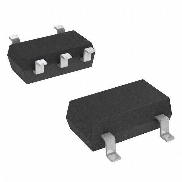
Product Sample & Technical Tools & Support & Folder Buy Documents Software Community TL1963A,TL1963A-15,TL1963A-18,TL1963A-25,TL1963A-33 SLVS719G–JUNE2008–REVISEDJANUARY2015 TL1963A-xx 1.5-A Low-Noise Fast-Transient-Response Low-Dropout Regulator 1 Features 3 Description • OptimizedforFastTransientResponse The TL1963A-xx devices are low-dropout (LDO) 1 regulators optimized for fast transient response. The • OutputCurrent:1.5A device can supply 1.5 A of output current with a • DropoutVoltage:340mV dropout voltage of 340 mV. Operating quiescent • LowNoise:40 μV (10Hzto100kHz) current is 1 mA, dropping to less than 1 μA in RMS shutdown.Quiescentcurrentiswellcontrolled;itdoes • 1-mAQuiescentCurrent not rise in dropout as with many other regulators. In • NoProtectionDiodesNeeded addition to fast transient response, the TL1963A-xx • ControlledQuiescentCurrentinDropout regulators have very low output noise, which makes themidealforsensitiveRFsupplyapplications. • FixedOutputVoltages:1.5V,1.8V,2.5V,3.3V • AdjustableOutputfrom1.21Vto20V(TL1963A DeviceInformation(1) Only) PARTNUMBER PACKAGE BODYSIZE(NOM) • LessThan1-μAQuiescentCurrentinShutdown SOT(6) 6.50mm×3.50mm • StableWith10-μFCeramicOutputCapacitor TL1963A TO-263(5) 10.16mm×8.42mm • Reverse-BatteryProtection SOT(6) 6.50mm×3.50mm • Reverse-CurrentProtection TL1963A-15 SOT(4) TO-263(5) 10.16mm×8.42mm 2 Applications SOT(6) 6.50mm×3.50mm • Industrial TL1963A-18 SOT(4) • WirelessInfrastructure TO-263(5) 10.16mm×8.42mm • Radio-FrequencySystems SOT(6) 6.50mm×3.50mm • 3.3-Vto2.5-VLogicPowerSupplies TL1963A-25 SOT(4) • PostRegulatorforSwitchingSupplies TO-263(5) 10.16mm×8.42mm SOT(6) 6.50mm×3.50mm TL1963A-33 SOT(4) TO-263(5) 10.16mm×8.42mm (1) For all available packages, see the orderable addendum at theendofthedatasheet. SimplifiedSchematic DropoutVoltagevsOutputCurrent 500 450 400 V 350 T =125°C m A – e 300 g a olt 250 V ut o 200 p o Dr 150 TA=25°C 100 50 0 0 0.2 0.4 0.6 0.8 1 1.2 1.4 1.6 OutputCurrent–A 1 An IMPORTANT NOTICE at the end of this data sheet addresses availability, warranty, changes, use in safety-critical applications, intellectualpropertymattersandotherimportantdisclaimers.PRODUCTIONDATA.
TL1963A,TL1963A-15,TL1963A-18,TL1963A-25,TL1963A-33 SLVS719G–JUNE2008–REVISEDJANUARY2015 www.ti.com Table of Contents 1 Features.................................................................. 1 9.3 FeatureDescription.................................................13 2 Applications........................................................... 1 9.4 DeviceFunctionalModes........................................15 3 Description............................................................. 1 10 ApplicationandImplementation........................ 16 4 RevisionHistory..................................................... 2 10.1 ApplicationInformation..........................................16 10.2 TypicalApplications..............................................16 5 Description(continued)......................................... 3 11 PowerSupplyRecommendations..................... 21 6 DeviceComparisonTable..................................... 3 12 Layout................................................................... 21 7 PinConfigurationandFunctions......................... 3 12.1 LayoutGuidelines.................................................21 8 Specifications......................................................... 5 12.2 LayoutExample....................................................22 8.1 AbsoluteMaximumRatings .....................................5 12.3 ThermalConsiderations........................................24 8.2 ESDRatings..............................................................5 13 DeviceandDocumentationSupport................. 26 8.3 RecommendedOperatingConditions.......................5 13.1 RelatedLinks........................................................26 8.4 ThermalInformation..................................................5 13.2 Trademarks...........................................................26 8.5 ElectricalCharacteristics...........................................6 13.3 ElectrostaticDischargeCaution............................26 8.6 TypicalCharacteristics..............................................8 13.4 Glossary................................................................26 9 DetailedDescription............................................ 13 14 Mechanical,Packaging,andOrderable 9.1 Overview.................................................................13 Information........................................................... 26 9.2 FunctionalBlockDiagram.......................................13 4 Revision History ChangesfromRevisionF(January2014)toRevisionG Page • AddedESDRatingstable,FeatureDescriptionsection,DeviceFunctionalModes,ApplicationandImplementation section,PowerSupplyRecommendationssection,Layoutsection,DeviceandDocumentationSupportsection,and Mechanical,Packaging,andOrderableInformationsection ................................................................................................. 1 2 SubmitDocumentationFeedback Copyright©2008–2015,TexasInstrumentsIncorporated ProductFolderLinks:TL1963A TL1963A-15 TL1963A-18 TL1963A-25 TL1963A-33
TL1963A,TL1963A-15,TL1963A-18,TL1963A-25,TL1963A-33 www.ti.com SLVS719G–JUNE2008–REVISEDJANUARY2015 5 Description (continued) Output voltage range is from 1.21 V to 20 V. The TL1963A-xx regulators are stable with output capacitance as low as 10 μF. Small ceramic capacitors can be used without the necessary addition of ESR as is common with other regulators. Internal protection circuitry includes reverse-battery protection, current limiting, thermal limiting, and reverse-current protection. The devices are available in fixed output voltages of 1.5 V, 1.8 V, 2.5 V, 3.3 V, andasanadjustabledevicewitha1.21-Vreferencevoltage. 6 Device Comparison Table DEVICE OUTPUTVOLTAGE PIN5(DCQANDKTTONLY) TL1963A Adjustable ADJ TL1963A-15 1.5V SENSE TL1963A-18 1.8V SENSE TL1963A-25 2.5V SENSE TL1963A-33 3.3V SENSE 7 Pin Configuration and Functions DCQ PACKAGE (TOPVIEW) 5 SENSE/ADJ 4 OUT D N 6 3 GND G 2 IN 1 SHDN DCY PACKAGE (TOPVIEW) 3 OUT D N 4 2 GND G 1 IN KTT PACKAGE (TOPVIEW) 5 SENSE/ADJ 4 OUT 3 GND IN 2 1 SHDN Copyright©2008–2015,TexasInstrumentsIncorporated SubmitDocumentationFeedback 3 ProductFolderLinks:TL1963A TL1963A-15 TL1963A-18 TL1963A-25 TL1963A-33
TL1963A,TL1963A-15,TL1963A-18,TL1963A-25,TL1963A-33 SLVS719G–JUNE2008–REVISEDJANUARY2015 www.ti.com PinFunctions PIN I/O DESCRIPTION NAME DCQ DCY KTT Adjust.FortheadjustableTL1963A,thisistheinputtotheerroramplifier.Thispinisclamped ADJ 5 — 5 I internallyto±7V.Ithasabiascurrentof3μAthatflowsintothepin.TheADJpinvoltageis 1.21Vreferencedtoground,andtheoutputvoltagerangeis1.21Vto20V. GND 3,6 2,4 3 — Ground Input.PowerissuppliedtothedevicethroughtheINpin.Abypasscapacitorisrequiredon thispinifthedeviceismorethansixinchesawayfromthemaininputfiltercapacitor.In general,theoutputimpedanceofabatteryriseswithfrequency,soitisadvisabletoincludea bypasscapacitorinbattery-poweredcircuits.Abypasscapacitor(ceramic)intherangeof IN 2 1 2 I 1μFto10μFissufficient.TheTL1963A-xxregulatorsaredesignedtowithstandreverse voltagesontheINpinwithrespecttogroundandtheOUTpin.Inthecaseofareverseinput, whichcanhappenifabatteryispluggedinbackwards,thedeviceactsasifthereisadiodein serieswithitsinput.Thereisnoreverse-currentflowintotheregulator,andnoreverse voltageappearsattheload.Thedeviceprotectsbothitselfandtheload. Output.Theoutputsuppliespowertotheload.Aminimumoutputcapacitor(ceramic)of OUT 4 3 4 O 10μFisrequiredtopreventoscillations.Largeroutputcapacitorsarerequiredforapplications withlargetransientloadstolimitpeakvoltagetransients. Sense.ForfixedvoltageversionsoftheTL1963A-xx(TL1963A-1.5,TL1963A-1.8,TL1963A- 2.5,andTL1963A-3.3),theSENSEpinistheinputtotheerroramplifier.Optimumregulation isobtainedatthepointwheretheSENSEpinisconnectedtotheOUTpinoftheregulator.In criticalapplications,smallvoltagedropsarecausedbytheresistance(R )ofPCtraces P betweentheregulatorandtheload.ThesemaybeeliminatedbyconnectingtheSENSEpin SENSE 5 — 5 I totheoutputattheloadasshowninFigure32.Notethatthevoltagedropacrosstheexternal PCBtracesaddstothedropoutvoltageoftheregulator.TheSENSEpinbiascurrentis600 μAattheratedoutputvoltage.TheSENSEpincanbepulledbelowground(asinadual supplysysteminwhichtheregulatorloadisreturnedtoanegativesupply)andstillallowthe devicetostartandoperate. Shutdown.TheSHDNpinisusedtoputtheTL1963A-xxregulatorsintoalow-power shutdownstate.TheoutputisoffwhentheSHDNpinispulledlow.TheSHDNpincanbe driveneitherby5-Vlogicoropen-collectorlogicwithapullupresistor.Thepullupresistoris SHDN 1 — 1 I requiredtosupplythepullupcurrentoftheopen-collectorgate,normallyseveral microamperes,andtheSHDNpincurrent,typically3μA.Ifunused,theSHDNpinmustbe connectedtoV .Thedeviceisinthelow-powershutdownstateiftheSHDNpinisnot IN connected. Thermal FortheKTTpackage,theexposedthermalpadisconnectedtogroundandmustbesoldered — — — — Pad tothePCBforratedthermalperformance. 4 SubmitDocumentationFeedback Copyright©2008–2015,TexasInstrumentsIncorporated ProductFolderLinks:TL1963A TL1963A-15 TL1963A-18 TL1963A-25 TL1963A-33
TL1963A,TL1963A-15,TL1963A-18,TL1963A-25,TL1963A-33 www.ti.com SLVS719G–JUNE2008–REVISEDJANUARY2015 8 Specifications 8.1 Absolute Maximum Ratings overoperatingvirtual-junctiontemperaturerange(unlessotherwisenoted) (1) MIN MAX UNIT IN –20 20 OUT –20 20 Input-to-outputdifferential(2) –20 20 Inputvoltage,V V IN SENSE –20 20 ADJ –7 7 SHDN –20 20 Outputshort-circuitduration,t Indefinite short Maximumleadtemperature(10-ssolderingtime),T 300 °C lead Maximumjunctiontemperature,T 125 °C JMAX Storagetemperature,T –65 150 °C stg (1) StressesbeyondthoselistedunderAbsoluteMaximumRatingsmaycausepermanentdamagetothedevice.Thesearestressratings only,andfunctionaloperationofthedeviceattheseoranyotherconditionsbeyondthoseindicatedunderRecommendedOperating Conditionsisnotimplied.Exposuretoconditionsbeyondtherecommendedoperatingmaximumforextendedperiodsmayaffectdevice reliability. (2) Absolutemaximuminput-to-outputdifferentialvoltagecannotbeachievedwithallcombinationsofratedINpinandOUTpinvoltages. WiththeINpinat20V,theOUTpinmaynotbepulledbelow0V.ThetotalmeasuredvoltagefromINtoOUTcannotexceed±20V. 8.2 ESD Ratings VALUE UNIT Humanbodymodel(HBM),perANSI/ESDA/JEDECJS-001(1) ±2000 V(ESD) Electrostaticdischarge Charged-devicemodel(CDM),perJEDECspecificationJESD22- ±1000 V C101(2) (1) JEDECdocumentJEP155statesthat500-VHBMallowssafemanufacturingwithastandardESDcontrolprocess. (2) JEDECdocumentJEP157statesthat250-VCDMallowssafemanufacturingwithastandardESDcontrolprocess. 8.3 Recommended Operating Conditions overoperatingfree-airtemperaturerange(unlessotherwisenoted) MIN MAX UNIT V Inputvoltagerange(1) V +V 20 V IN OUT DO V SHDNHigh-LevelInputVoltage 2 20 V IH V SHDNLow-LevelInputVoltage 0.25 V IL T Recommendedoperatingjunctiontemperaturerange –40 125 °C J (1) TL1963A,TL1963A-15,andTL1963A-18mayrequireahigherminimuminputvoltageundersomeoutputvoltage/loadconditionsas indicatedunderElectricalCharacteristics. 8.4 Thermal Information TL1963A-xx THERMALMETRIC(1)(2) KTT DCQ DCY UNIT 5PINS 6PINS 4PINS R Junction-to-ambientthermalresistance 32.9 50.5 57.9 θJA R Junction-to-case(top)thermalresistance 37.6 31.1 38.6 θJC(top) R Junction-to-boardthermalresistance 18.9 5.1 7.1 θJB °C/W ψ Junction-to-topcharacterizationparameter 5.7 1.0 1.7 JT ψ Junction-to-boardcharacterizationparameter 17.3 5.0 7.0 JB R Junction-to-case(bottom)thermalresistance 1.0 — — θJC(bot) (1) Formoreinformationabouttraditionalandnewthermalmetrics,seetheICPackageThermalMetricsapplicationreport,SPRA953. (2) ForthermalestimatesofthisdevicebasedonPCBcopperarea,seetheTIPCBThermalCalculator. Copyright©2008–2015,TexasInstrumentsIncorporated SubmitDocumentationFeedback 5 ProductFolderLinks:TL1963A TL1963A-15 TL1963A-18 TL1963A-25 TL1963A-33
TL1963A,TL1963A-15,TL1963A-18,TL1963A-25,TL1963A-33 SLVS719G–JUNE2008–REVISEDJANUARY2015 www.ti.com 8.5 Electrical Characteristics OverrecommendedoperatingtemperaturerangeT =–40to125°C(unlessotherwisenoted)(1) J PARAMETER TESTCONDITIONS T MIN TYP(2) MAX UNIT J I =0.5A 25°C 1.9 V Minimuminputvoltage(3)(4) LOAD V IN I =1.5A Fullrange 2.1 2.5 LOAD V =2.21V,I =1mA 25°C 1.477 1.5 1.523 IN LOAD TL1963A-15 V =2.5Vto20V, IN Fullrange 1.447 1.5 1.545 I =1mAto1.5A LOAD V =2.3V,I =1mA 25°C 1.773 1.8 1.827 IN LOAD TL1963A-18 V =2.8Vto20V, IN Fullrange 1.737 1.8 1.854 I =1mAto1.5A V Regulatedoutputvoltage(5) LOAD V OUT V =3V,I =1mA 25°C 2.462 2.5 2.538 IN LOAD TL1963A-25 V =3.5Vto20V, IN Fullrange 2.412 2.5 2.575 I =1mAto1.5A LOAD V =3.8V,I =1mA 25°C 3.25 3.3 3.35 IN LOAD TL1963A-33 V =4.3Vto20V, IN Fullrange 3.2 3.3 3.4 I =1mAto1.5A LOAD V =2.21V,I =1mA 25°C 1.192 1.21 1.228 IN LOAD VADJ ADJpinvoltage(3)(5) TL1963A VIN=2.5Vto20V, Fullrange 1.174 1.21 1.246 V I =1mAto1.5A LOAD ΔV =2.21Vto20V, TL1963A-15 IN Fullrange 2 6 I =1mA LOAD ΔV =2.3Vto20V, TL1963A-18 IN Fullrange 2.5 7 I =1mA LOAD ΔV =3Vto20V, Lineregulation TL1963A-25 IN Fullrange 3 10 mV I =1mA LOAD ΔV =3.8Vto20V, TL1963A-33 IN Fullrange 3.5 10 I =1mA LOAD TL1963A(3) ΔVIN=2.21Vto20V, Fullrange 1.5 5 I =1mA LOAD V =2.5V, 25°C 2 9 TL1963A-15 IN ΔILOAD=1mAto1.5A Fullrange 18 V =2.8V, 25°C 2 10 TL1963A-18 IN ΔILOAD=1mAto1.5A Fullrange 20 V =3.5V, 25°C 2.5 15 Loadregulation TL1963A-25 IN mV ΔILOAD=1mAto1.5A Fullrange 30 V =4.3V, 25°C 3 20 TL1963A-33 IN ΔILOAD=1mAto1.5A Fullrange 70 TL1963A(3) VIN=2.5V, 25°C 2 8 ΔILOAD=1mAto1.5A Fullrange 18 (1) TheTL1963A-xxregulatorsaretestedandspecifiedunderpulseloadconditionssuchthatT ≉T .TheyarefullytestedatT =25°C. J A A Performanceat–40and125°Cisspecifiedbydesign,characterization,andcorrelationwithstatisticalprocesscontrols. (2) Typicalvaluesrepresentthelikelyparametricnominalvaluesdeterminedatthetimeofcharacterization.Typicalvaluesdependonthe applicationandconfigurationandmayvaryovertime.Typicalvaluesarenotensuredonproductionmaterial. (3) TheTL1963AistestedandspecifiedfortheseconditionswiththeADJpinconnectedtotheOUTpin. (4) FortheTL1963A,TL1963A-15andTL1963A-18,dropoutvoltagesarelimitedbytheminimuminputvoltagespecificationundersome outputvoltage/loadconditions. (5) Operatingconditionsarelimitedbymaximumjunctiontemperature.Theregulatedoutputvoltagespecificationdoesnotapplyforall possiblecombinationsofinputvoltageandoutputcurrent.Whenoperatingatmaximuminputvoltage,theoutputcurrentrangemustbe limited.Whenoperatingatmaximumoutputcurrent,theinputvoltagerangemustbelimited. 6 SubmitDocumentationFeedback Copyright©2008–2015,TexasInstrumentsIncorporated ProductFolderLinks:TL1963A TL1963A-15 TL1963A-18 TL1963A-25 TL1963A-33
TL1963A,TL1963A-15,TL1963A-18,TL1963A-25,TL1963A-33 www.ti.com SLVS719G–JUNE2008–REVISEDJANUARY2015 Electrical Characteristics (continued) OverrecommendedoperatingtemperaturerangeT =–40to125°C(unlessotherwisenoted)(1) J PARAMETER TESTCONDITIONS T MIN TYP(2) MAX UNIT J 25°C 0.02 0.06 I =1mA LOAD Fullrange 0.1 25°C 0.1 0.17 I =100mA LOAD Dropoutvoltage(4)(6)(7) Fullrange 0.22 V V DO VIN=VOUT(NOMINAL) 25°C 0.19 0.27 I =500mA LOAD Fullrange 0.35 25°C 0.34 0.45 I =1.5A LOAD Fullrange 0.55 I =0mA Fullrange 1 1.5 LOAD I =1mA Fullrange 1.1 1.6 LOAD GNDpincurrent(7)(8) I I =100mA Fullrange 3.8 5.5 mA GND V =V +1 LOAD IN OUT(NOMINAL) I =500mA Fullrange 15 25 LOAD I =1.5A Fullrange 80 120 LOAD C =10μF,I =1.5A, e Outputvoltagenoise OUT LOAD 25°C 40 μV N B =10Hzto100kHz RMS W I ADJpinbiascurrent(3)(9) 25°C 3 10 μA ADJ V =OFFtoON Fullrange 0.9 2 OUT Shutdownthreshold V V =ONtoOFF Fullrange 0.25 0.75 OUT V =0V 25°C 0.01 1 SHDN I SHDNpincurrent μA SHDN V =20V 25°C 3 30 SHDN Quiescentcurrentinshutdown V =6V,V =0V 25°C 0.01 1 μA IN SHDN V –V =1.5V(avg),V =0.5V , Ripplerejection IN OUT RIPPLE P-P 25°C 55 63 dB f =120Hz,I =0.75A RIPPLE LOAD V =7V,V =0V 25°C 2 IN OUT I Currentlimit A LIMIT V =V +1 Fullrange 1.6 IN OUT(NOMINAL) I Inputreverseleakagecurrent V =–20V,V =0V Fullrange 1 μA IL IN OUT TL1963A-15 V =1.5V,V <1.5V 25°C 600 1200 OUT IN TL1963A-18 V =1.8V,V <1.8V 25°C 600 1200 OUT IN I Reverseoutputcurrent(10) TL1963A-25 V =2.5V,V <2.5V 25°C 600 1200 μA RO OUT IN TL1963A-33 V =3.3V,V <3.3V 25°C 600 1200 OUT IN TL1963A V =1.21V,V <1.21V 25°C 300 600 OUT IN (6) Dropoutvoltageistheminimuminputtooutputvoltagedifferentialneededtomaintainregulationataspecifiedoutputcurrent.In dropout,theoutputvoltageisequalto:V –V . IN DROPOUT (7) Tosatisfyrequirementsforminimuminputvoltage,theTL1963Aistestedandspecifiedfortheseconditionswithanexternalresistor divider(two4.12-kΩresistors)foranoutputvoltageof2.4V.Theexternalresistordivideraddsa300-µADCloadontheoutput. (8) GNDpincurrentistestedwithV =(V +1V)andacurrentsourceload.TheGNDpincurrentdecreasesathigherinput IN OUT(NOMINAL) voltages. (9) ADJpinbiascurrentflowsintotheADJpin. (10) ReverseoutputcurrentistestedwiththeINpingroundedandtheOUTpinforcedtotheratedoutputvoltage.Thiscurrentflowsintothe OUTpinandouttheGNDpin. Copyright©2008–2015,TexasInstrumentsIncorporated SubmitDocumentationFeedback 7 ProductFolderLinks:TL1963A TL1963A-15 TL1963A-18 TL1963A-25 TL1963A-33
TL1963A,TL1963A-15,TL1963A-18,TL1963A-25,TL1963A-33 SLVS719G–JUNE2008–REVISEDJANUARY2015 www.ti.com 8.6 Typical Characteristics TypicalcharacteristicsapplytoallTL1963A-xxdevicesunlessotherwisenoted. 500 480 450 IOUT=1.5A 400 360 mV350 TA=125°C mV DropoutVoltage–122350500000 TA=25°C DropoutVoltage–240 IOUT=0.5A 120 IOUT=100mA 100 50 IOUT=1mA 0 0 0 0.2 0.4 0.6 0.8 1 1.2 1.4 1.6 -50 -25 0 25 50 75 100 125 OutputCurrent–A TA–Free-AirTemperature–°C Figure1.DropoutVoltagevsOutputCurrent Figure2.DropoutVoltagevsTemperature 1.5 1.4 VIN=6V IOUT=0A 1.3 VSHDN=VIN mA1.2 – Current1.11 VOTULT1F9i6x3eAd-33..33V nt ce0.9 s e Qui0.8 TVLO1U9T6A3dAju(Astdajbusletable) 0.7 0.6 0.5 -50 -25 0 25 50 75 100 125 TA–Free-AirTemperature–°C VIN=6V IOUT=0A VSHDN=VIN IOUT=1mA TL1963A-18 Figure3.QuiescentCurrentvsTemperature Figure4.TL1963A-18OutputVoltagevsTemperature I =1mA TL1963A-25 I =1mA TL1963A-33 OUT OUT Figure5.TL1963A-25OutputVoltagevsTemperature Figure6.TL1963A-33OutputVoltagevsTemperature 8 SubmitDocumentationFeedback Copyright©2008–2015,TexasInstrumentsIncorporated ProductFolderLinks:TL1963A TL1963A-15 TL1963A-18 TL1963A-25 TL1963A-33
TL1963A,TL1963A-15,TL1963A-18,TL1963A-25,TL1963A-33 www.ti.com SLVS719G–JUNE2008–REVISEDJANUARY2015 Typical Characteristics (continued) TypicalcharacteristicsapplytoallTL1963A-xxdevicesunlessotherwisenoted. 1.23 1.2 1.225 1 1.22 A) Output Voltage (V) 111..22.201155 uiescent Current (m 000...468 1.2 Q 0.2 1.195 1.19 0 -50 -25 0 25 50 75 100 125 0 2 4 6 8 10 12 14 16 18 20 Free-Air Temperature (qC) D020 Input Voltage (V) D021 IOUT=1mA VIN=6V TJ=25°C ROUT=4.3kΩ VSHDN=VIN Figure7.TL1963AOutputVoltagevsTemperature Figure8.QuiescentCurrentvsInputVoltage 10 9 IIOOUUTT == 1100 0m mAA 8 IOUT = 300 mA A) 7 m nt ( 6 e urr 5 C d 4 n u Gro 3 2 1 0 0 1 2 3 4 5 6 7 8 9 10 Input Voltage (V) D022 TJ=25°C VOUT=1.21V VSHDN=VIN TJ=25°C VOUT=1.21V VSHDN=VIN Figure9.TL1963AGroundCurrentvsInputVoltage Figure10.TL1963AGroundCurrentvsInputVoltage T =25°C V =V J SHDN IN T =25°C V =V J SHDN IN Figure11.TL1963A-33GroundCurrentvsInputVoltage Figure12.TL1963A-33GroundCurrentvsInputVoltage Copyright©2008–2015,TexasInstrumentsIncorporated SubmitDocumentationFeedback 9 ProductFolderLinks:TL1963A TL1963A-15 TL1963A-18 TL1963A-25 TL1963A-33
TL1963A,TL1963A-15,TL1963A-18,TL1963A-25,TL1963A-33 SLVS719G–JUNE2008–REVISEDJANUARY2015 www.ti.com Typical Characteristics (continued) TypicalcharacteristicsapplytoallTL1963A-xxdevicesunlessotherwisenoted. VIN=VOUT(nom)+1 VSHDN=0V Figure13.GroundCurrentvsOutputCurrent Figure14.QuiescentCurrentinShutdownvsInputVoltage 1 2.5 2.25 A) 0.75 2 urrent (P ent–µA11.7.55 ut C 0.5 Curr1.25 np ut DN I NInp 1 H 0.25 D S H0.75 S 0.5 0 0.25 -50 -25 0 25 50 75 100 125 Free-Air Temperature (qC) 0 D011 0 2 4 6 8 10 12 14 16 18 20 V =0V SHON SHDNInputVoltage–V Figure15.SHDNPinCurrent(I )vsTemperature Figure16. SHDNPinCurrent(I )vsSHDNInputVoltage SHDN SHDN I =1mA I =1mA OUT OUT Figure17. SHDNThreshold(OFFtoON)vsTemperature Figure18. SHDNThreshold(ONtoOFF)vsTemperature 10 SubmitDocumentationFeedback Copyright©2008–2015,TexasInstrumentsIncorporated ProductFolderLinks:TL1963A TL1963A-15 TL1963A-18 TL1963A-25 TL1963A-33
TL1963A,TL1963A-15,TL1963A-18,TL1963A-25,TL1963A-33 www.ti.com SLVS719G–JUNE2008–REVISEDJANUARY2015 Typical Characteristics (continued) TypicalcharacteristicsapplytoallTL1963A-xxdevicesunlessotherwisenoted. 5 4.5 4 A3.5 µ – Current2.53 Bias 2 DJ A1.5 1 0.5 0 -50 -25 0 25 50 75 100 125 TA–Free-AirTemperature–°C ΔV =100mV OUT Figure19.ADJBiasCurrentvsTemperature Figure20.CurrentLimitvsInput-to-OutputDifferential Voltage 12 TJ=25°C 10 VIN=0V CurrentflowsintoOUTpin A m – 8 nt e urr 6 TL196V3OAUT(AAddjjuussttaabbllee) utC VOUT=V VOAUDTJ=VADJ p ut 4 O e s ver 2 e R 0 VOTULT1F9ix6e3dA-33..33V VOVUOTU=T=V FVBFB -2 0 2 4 6 8 10 OutputVoltage–V T =25°C V =0V J IN V =7V V =0V CurrentflowsintoOUTpin IN OUT Figure21.CurrentLimitvsTemperature Figure22.ReverseOutputCurrentvsOutputVoltage 1000 VIN=0V 800 A µ – nt e urr 600 C utput VVOOTVUULOTTU1F=T9=i3x6 .e333d.A3V- 33V..33V O 400 e s er v e R 200 VTOLU1T9A63dAju(sAtadbjulestable) VVOOUUTT== 11..2211 VV 0 -50 -25 0 25 50 75 100 125 V =0.05V C =0 T =25°C TA–Free-AirTemperature–°C RIPPLE PP IN A VIN=0V VIN=2.7V COUT=10µF(ceramic) Figure23.ReverseOutputCurrentvsTemperature Figure24.RippleRejectionvsFrequency Copyright©2008–2015,TexasInstrumentsIncorporated SubmitDocumentationFeedback 11 ProductFolderLinks:TL1963A TL1963A-15 TL1963A-18 TL1963A-25 TL1963A-33
TL1963A,TL1963A-15,TL1963A-18,TL1963A-25,TL1963A-33 SLVS719G–JUNE2008–REVISEDJANUARY2015 www.ti.com Typical Characteristics (continued) TypicalcharacteristicsapplytoallTL1963A-xxdevicesunlessotherwisenoted. 20 1 IOUT=1.5A 15 COUTC=O 1UT0 =µF10 (cµeFramic) 10 IOUT=IO U1T.5=A1.5A gulation–mV-1-0505 TL196V3OAUT(AAddjjuussttaabbllee) ÖVoltage–µV/HzVoltage–µVRMS 0.1 VTLOU1T9F6i3xAe-d3.33.3V LoadRe--2105 VOTULT1F9Vix6OTe3ULdAT1F-191i.6x.883eVAd-22..55V utput Noise utputNoise TL1V9O6U3TAAd(Ajudsjutasbtaleble) -25 OO VOTULT1F9i6x3eAd-33..33V -30 -35 -50 -25 0 25 50 75 100 125 0.01 10 100 1k 10k 100k TA–Free-AirTemperature–°C Frequency-Hz IOUT=1mAto1.5A COUT=10µF IOUT=1.5A (ceramic) Figure25.LoadRegulationvsTemperature Figure26.OutputNoiseVoltagevsFrequency V =4.3V C =10µF V =4.3V C =10µF IN IN IN IN C =10µF(ceramic) C =10µF(ceramic) OUT OUT Figure27.LoadTransientResponse Figure28.LoadTransientResponse I =1.5A C =10µF OUT IN C =10µF(ceramic) OUT Figure29.LineTransientresponse 12 SubmitDocumentationFeedback Copyright©2008–2015,TexasInstrumentsIncorporated ProductFolderLinks:TL1963A TL1963A-15 TL1963A-18 TL1963A-25 TL1963A-33
TL1963A,TL1963A-15,TL1963A-18,TL1963A-25,TL1963A-33 www.ti.com SLVS719G–JUNE2008–REVISEDJANUARY2015 9 Detailed Description 9.1 Overview The TL1963A-xx series are 1.5-A low-dropout regulators optimized for fast transient response. The devices can supply1.5Aatadropoutvoltageof340mV.Thelowoperatingquiescentcurrent(1mA)dropstolessthan1 μA in shutdown. In addition to the low quiescent current, the TL1963A-xx regulators incorporate several protection features that make them ideal for use in battery-powered systems. The devices are protected against both reverse input and reverse output voltages. In battery-backup applications where the output can be held up by a backup battery when the input is pulled to ground, the TL1963A-xx acts as if it has a diode in series with its output and prevents reverse-current flow. Additionally, in dual-supply applications where the regulator load is returned to a negative supply, the output can be pulled below ground by as much as (20 V – VIN) and still allow thedevicetostartandoperate. 9.2 Functional Block Diagram 9.3 Feature Description 9.3.1 OverloadRecovery Like many IC power regulators, the TL1963A-xx has safe operating area protection. The safe area protection decreases the current limit as input-to-output voltage increases and keeps the power transistor inside a safe operating region for all values of input-to-output voltage. The protection is designed to provide some output currentatallvaluesofinput-to-outputvoltageuptothedevicebreakdown. When power is first turned on, as the input voltage rises, the output follows the input, allowing the regulator to start up into very heavy loads. During start-up, as the input voltage is rising, the input-to-output voltage differential is small, allowing the regulator to supply large output currents. With a high input voltage, a problem can occur wherein removal of an output short does not allow the output voltage to recover. Other regulators also exhibitthisphenomenon,soitisnotuniquetotheTL1963A-xx. Copyright©2008–2015,TexasInstrumentsIncorporated SubmitDocumentationFeedback 13 ProductFolderLinks:TL1963A TL1963A-15 TL1963A-18 TL1963A-25 TL1963A-33
TL1963A,TL1963A-15,TL1963A-18,TL1963A-25,TL1963A-33 SLVS719G–JUNE2008–REVISEDJANUARY2015 www.ti.com Feature Description (continued) The problem occurs with a heavy output load when the input voltage is high and the output voltage is low. Common situations occur immediately after the removal of a short circuit or when the shutdown pin is pulled high after the input voltage has already been turned on. The load line for such a load may intersect the output current curve at two points. If this happens, there are two stable output operating points for the regulator. With this double intersection, the input power supply may need to be cycled down to zero and brought up again to make theoutputrecover. 9.3.2 OutputVoltageNoise The TL1963A-xx regulators have been designed to provide low output voltage noise over the 10-Hz to 100-kHz bandwidth while operating at full load. Output voltage noise is typically 35 nV/√Hz over this frequency bandwidth for the TL1963A (adjustable version). For higher output voltages (generated by using a resistor divider), the output voltage noise is gained up accordingly. This results in RMS noise over the 10-Hz to 100-kHz bandwidth of 14μV fortheTL1963A,increasingto38 μV fortheTL1963A-33. RMS RMS Higher values of output voltage noise may be measured when care is not exercised with regard to circuit layout and testing. Crosstalk from nearby traces can induce unwanted noise onto the output of the TL1963A-xx. Power- supply ripple rejection must also be considered; the TL1963A-xx regulators do not have unlimited power-supply rejectionandpassasmallportionoftheinputnoisethroughtotheoutput. 9.3.3 ProtectionFeatures The TL1963A-xx regulators incorporate several protection features which make them ideal for use in battery- powered circuits. In addition to the normal protection features associated with monolithic regulators, such as current limiting and thermal limiting, the devices are protected against reverse input voltages, reverse output voltagesandreversevoltagesfromoutputtoinput. Current limit protection and thermal overload protection are intended to protect the device against current overloadconditionsattheoutputofthedevice.Fornormaloperation,thejunctiontemperatureshouldnotexceed 125°C. The input of the device withstands reverse voltages of 20 V. Current flow into the device is limited to less than 1 mA (typically less than 100 μA), and no negative voltage appears at the output. The device protects both itself andtheload.Thisprovidesprotectionagainstbatteriesthatcanbepluggedinbackward. The output of the TL1963A-xx can be pulled below ground without damaging the device. If the input is left open circuit or grounded, the output can be pulled below ground by 20 V. For fixed voltage versions, the output acts like a large resistor, typically 5 kΩ or higher, limiting current flow to typically less than 600 μA. For adjustable versions, the output acts like an open circuit; no current flows out of the pin. If the input is powered by a voltage source, the output sources the short-circuit current of the device and protects itself by thermal limiting. In this case,groundingtheSHDNpinturnsoffthedeviceandstopstheoutputfromsourcingtheshort-circuitcurrent. The ADJ pin of the adjustable device can be pulled above or below ground by as much as 7 V without damaging the device. If the input is left open circuit or grounded, the ADJ pin acts like an open circuit when pulled below groundandlikealargeresistor(typically5kΩ)inserieswithadiodewhenpulledaboveground. In situations where the ADJ pin is connected to a resistor divider that would pull the ADJ pin above its 7-V clamp voltage if the output is pulled high, the ADJ pin input current must be limited to less than 5 mA. For example, a resistordividerisusedtoprovidearegulated1.5-Voutputfromthe1.21-Vreferencewhentheoutputisforcedto 20 V. The top resistor of the resistor divider must be chosen to limit the current into the ADJ pin to less than 5 mA when the ADJ pin is at 7 V. The 13-V difference between OUT and ADJ divided by the 5-mA maximum currentintotheADJpinyieldsaminimumtopresistorvalueof2.6kΩ. In circuits where a backup battery is required, several different input/output conditions can occur. The output voltage may be held up while the input is either pulled to ground, pulled to some intermediate voltage, or is left opencircuit. When the IN pin of the TL1963A-xx is forced below the OUT pin or the OUT pin is pulled above the IN pin, input current typically drops to less than 2 μA. This can happen if the input of the device is connected to a discharged (low voltage) battery and the output is held up by either a backup battery or a second regulator circuit. The state oftheSHDNpinhasnoeffectonthereverseoutputcurrentwhentheoutputispulledabovetheinput. 14 SubmitDocumentationFeedback Copyright©2008–2015,TexasInstrumentsIncorporated ProductFolderLinks:TL1963A TL1963A-15 TL1963A-18 TL1963A-25 TL1963A-33
TL1963A,TL1963A-15,TL1963A-18,TL1963A-25,TL1963A-33 www.ti.com SLVS719G–JUNE2008–REVISEDJANUARY2015 9.4 Device Functional Modes Table1.DeviceStates SHDN DEVICESTATE H RegulatedVoltage L Shutdown Copyright©2008–2015,TexasInstrumentsIncorporated SubmitDocumentationFeedback 15 ProductFolderLinks:TL1963A TL1963A-15 TL1963A-18 TL1963A-25 TL1963A-33
TL1963A,TL1963A-15,TL1963A-18,TL1963A-25,TL1963A-33 SLVS719G–JUNE2008–REVISEDJANUARY2015 www.ti.com 10 Application and Implementation NOTE Information in the following applications sections is not part of the TI component specification, and TI does not warrant its accuracy or completeness. TI’s customers are responsible for determining suitability of components for their purposes. Customers should validateandtesttheirdesignimplementationtoconfirmsystemfunctionality. 10.1 Application Information This section will highlight some of the design considerations when implementing this device in various applications. 10.1.1 OutputCapacitanceandTransientResponse The TL1963A-xx regulators are designed to be stable with a wide range of output capacitors. The ESR of the output capacitor affects stability, most notably with small capacitors. A minimum output capacitor of 10 μF with anESRof3Ω orlessisrecommendedtopreventoscillations.Largervaluesofoutputcapacitancecandecrease the peak deviations and provide improved transient response for larger load current changes. Bypass capacitors, used to decouple individual components powered by the TL1963A-xx, increase the effective output capacitor value. Extra consideration must be given to the use of ceramic capacitors. Ceramic capacitors are manufactured with a variety of dielectrics, each with different behavior over temperature and applied voltage. The most common dielectrics used are Z5U, Y5V, X5R and X7R. The Z5U and Y5V dielectrics are good for providing high capacitances in a small package, but exhibit strong voltage and temperature coefficients. When used with a 5-V regulator, a 10-μF Y5V capacitor can exhibit an effective value as low as 1 μF to 2 μF over the operating temperature range. The X5R and X7R dielectrics result in more stable characteristics and are more suitable for use as the output capacitor. The X7R type has better stability across temperature, while the X5R is less expensiveandisavailableinhighervalues. Voltage and temperature coefficients are not the only sources of problems. Some ceramic capacitors have a piezoelectric response. A piezoelectric device generates voltage across its terminals due to mechanical stress, similar to the way a piezoelectric accelerometer or microphone works. For a ceramic capacitor, the stress can be inducedbyvibrationsinthesystemorthermaltransients. 10.2 Typical Applications 10.2.1 AdjustableOutputOperation NOTE: Allcapacitorsareceramic. Figure30. AdjustableOutputVoltageOperation 16 SubmitDocumentationFeedback Copyright©2008–2015,TexasInstrumentsIncorporated ProductFolderLinks:TL1963A TL1963A-15 TL1963A-18 TL1963A-25 TL1963A-33
TL1963A,TL1963A-15,TL1963A-18,TL1963A-25,TL1963A-33 www.ti.com SLVS719G–JUNE2008–REVISEDJANUARY2015 Typical Applications (continued) 10.2.1.1 DesignRequirements Table2.DesignParameters DESIGNPARAMETER EXAMPLEVALUE InputVoltage(V ) 5.0V IN OutputVoltage(V ) 2.5V OUT OutputCurrent(I ) 0Ato1A OUT LoadRegulation 1% 10.2.1.2 DetailedDesignProcedure The TL1963A has an adjustable output voltage range of 1.21 V to 20 V. The output voltage is set by the ratio of two external resistors R1 and R2 as shown in Figure 30. The device maintains the voltage at the ADJ pin at 1.21 V referenced to ground. The current in R1 is then equal to (1.21 V/R1), and the current in R2 is the current in R1 plus the ADJ pin bias current. The ADJ pin bias current, 3 µA at 25°C, flows through R2 into the ADJ pin. The outputvoltagecanbecalculatedusingEquation1. R2 V =1.21V(1+ )+I ´R2 OUT ADJ R1 (1) The value of R1 should be less than 4.17 kΩ to minimize errors in the output voltage caused by the ADJ pin bias current. Note that in shutdown the output is turned off, and the divider current is zero. For an output voltage of 2.50V,R1willbesetto4.0kΩ.R2isthenfoundtobe4.22kΩ usingtheequationabove. 4.22kW V =1.21V(1+ )+3µA´4.22kW OUT 4.0kW (2) V =2.50V (3) OUT The adjustable device is tested and specified with the ADJ pin tied to the OUT pin for an output voltage of 1.21 V.Specificationsforoutputvoltagesgreaterthan1.21Vareproportionaltotheratioofthedesiredoutputvoltage to1.21V:V /1.21V.Forexample,loadregulationforanoutputcurrentchangeof1mAto1.5Ais –2mV(typ) OUT atV =1.21V.AtV =2.50V,thetypicalloadregulationis: OUT OUT (2.50V/1.21V)(–2mV)=–4.13mV (4) Figure 33 shows the actual change in output is ~3 mV for a 1A load step. The maximum load regulation at 25 °C is–8mV.AtV =2.50V,themaximumloadregulationis: OUT (2.50V/1.21V)(–8mV)=–16.53mV (5) Since16.53mVisonly0.7%ofthe2.5Voutputvoltage,theloadregulationwillmeetthedesignrequirements. 10.2.1.2.1 FixedOperation The TL1963A-xx can be used in a fixed voltage configuration. The SENSE/ADJ pin should be connected to OUT for proper operation. An example of this is shown in Figure 31. The TL1963A can also be used in this configurationforafixedoutputvoltageof1.21V. IN OUT 2.5V at 1.5 A 10 µF 10 µF TL1963A-2.5 VIN> 3V (ceramic) (ceramic) SHDN SENSE GND Figure31. 3.3-Vto2.5-VRegulator During fixed voltage operation, the SENSE/ADJ pin can be used for a Kelvin connection if routed separately to the load. This allows the regulator to compensate for voltage drop across parasitic resistances (RP) between the outputandtheload.Thisbecomesmorecrucialwithhigherloadcurrents. Copyright©2008–2015,TexasInstrumentsIncorporated SubmitDocumentationFeedback 17 ProductFolderLinks:TL1963A TL1963A-15 TL1963A-18 TL1963A-25 TL1963A-33
TL1963A,TL1963A-15,TL1963A-18,TL1963A-25,TL1963A-33 SLVS719G–JUNE2008–REVISEDJANUARY2015 www.ti.com RP IN OUT TL1963A VIN SHDN SENSE Load GND RP Figure32. KelvinSenseConnection 10.2.1.3 ApplicationCurve Figure33. 1-ALoadTransientResponse(C =10uF) OUT 18 SubmitDocumentationFeedback Copyright©2008–2015,TexasInstrumentsIncorporated ProductFolderLinks:TL1963A TL1963A-15 TL1963A-18 TL1963A-25 TL1963A-33
TL1963A,TL1963A-15,TL1963A-18,TL1963A-25,TL1963A-33 www.ti.com SLVS719G–JUNE2008–REVISEDJANUARY2015 10.2.2 ParallelingRegulatorsforHigherOutputCurrent NOTE: Allcapacitorsareceramic. Figure34. ParallelingRegulatorsForHigherOutputCurrent 10.2.2.1 DesignRequirements Table3.DesignParameters DESIGNPARAMETER EXAMPLEVALUE InputVoltage(V ) 6.0V IN OutputVoltage(V ) 3.3V OUT OutputCurrent(I ) 3.0A OUT 10.2.2.2 DetailedDesignProcedure In an application requiring higher output current, an adjustable output regular can be placed in parallel with a fixed output regulator to increase the current capacity. Two sense resistors and a comparator can be used to controlthefeedbackloopoftheadjustableregulatorinordertobalancethecurrentbetweenthetworegulators. In Figure 34 resistors R1 and R2 are used to sense the current flowing into each regulator and should have a very low resistance to avoid unnecessary power loss. R1 and R2 should have the same value and a tolerance of 1% or better so the current is shared equally between the regulators. For this example, a value of 0.01 Ω will be used. Copyright©2008–2015,TexasInstrumentsIncorporated SubmitDocumentationFeedback 19 ProductFolderLinks:TL1963A TL1963A-15 TL1963A-18 TL1963A-25 TL1963A-33
TL1963A,TL1963A-15,TL1963A-18,TL1963A-25,TL1963A-33 SLVS719G–JUNE2008–REVISEDJANUARY2015 www.ti.com The TLV3691 rail-to-rail nanopower comparator output will alternate between VIN and GND depending on the currents flowing into each of the two regulators. To design this control circuit, begin by looking at the case where the two output currents are approximately equal and the comparator output is low. In this case, the output of the TL1963A should be set the same as the fixed voltage regulator. The TL1963A-33 has a 3.3 V fixed output, so this will be the set point for the adjustable regulator. Begin by selecting a R7 value less than 4.17 kΩ. In this example, 3.3 kΩ will be used. R5 will need to have a high resistance to satisfy Equation 10, for this example 100 kΩ was chosen. Then find the parallel resistance of R5 and R7 since they are both connected from the ADJ pin toGNDusingEquation6. R5´R7 (R5||R7)= =3.19kΩ R5+R7 (6) OncetheR5andR7parallelresistanceincalculated,thevalueforR6canbefoundusingEquation7. V R6= OUT (R5||R7)-(R5||R7) 1.22V (7) 3.3V R6= (3.19kW)-(3.19kW) 1.22V (8) R6=5.45kΩ (9) In the case where the TL1963A-33 is sourcing more current than TL1963A, the comparator output will go high. This will lower the voltage at the ADJ pin causing the TL1963A to try and raise the output voltage by sourcing more current. The TL1963A-33 will then react by sourcing less current to try and keep the output from rising. When the current through the TL1963A-33 becomes less than the TL1963A, the comparator output will return to GND.Inorderforthistohappen,Equation10mustbesatisfied: æ R7 ö æ R6 ö VINçèR5+R7÷ø+(VIN-VOUT)çèR5+R6÷ø< Vref (10) æ 3.3kW ö æ 5.45kW ö 6Vç ÷+(2.7V)ç ÷ <1.21V è100kW+3.3kWø è100kW+5.45kWø (11) 0.19V+0.14V<1.21V (12) 0.33V<1.21V (13) 10.2.2.3 ApplicationCurve Figure35. ParallelRegulatorsSharingLoadCurrent 20 SubmitDocumentationFeedback Copyright©2008–2015,TexasInstrumentsIncorporated ProductFolderLinks:TL1963A TL1963A-15 TL1963A-18 TL1963A-25 TL1963A-33
TL1963A,TL1963A-15,TL1963A-18,TL1963A-25,TL1963A-33 www.ti.com SLVS719G–JUNE2008–REVISEDJANUARY2015 11 Power Supply Recommendations The device is designed to operate with an input voltage supply up to 20 V. The minimum input voltage should provideadequateheadroomgreaterthanthedropoutvoltageinorderforthedevicetohavearegulatedoutput.If the input supply is noisy, additional input capacitors with low ESR can help improve the output noise performance. 12 Layout 12.1 Layout Guidelines • Forbestperformance,alltracesshouldbeasshortaspossible. • UsewidetracesforIN,OUT,andGNDtominimizetheparasiticelectricaleffects. • Aminimumoutputcapacitorof10μFwithanESRof3Ω orlessisrecommendedtopreventoscillations.X5R andX7Rdielectricsarepreferred. • PlacetheOutputCapacitorascloseaspossibletotheOUTpinofthedevice. • ThetaboftheDCQpackageshouldbeconnectedtoground. • The exposed thermal pad of the KTT package should be connected to a wide ground plane for effective heat dissipation. Copyright©2008–2015,TexasInstrumentsIncorporated SubmitDocumentationFeedback 21 ProductFolderLinks:TL1963A TL1963A-15 TL1963A-18 TL1963A-25 TL1963A-33
TL1963A,TL1963A-15,TL1963A-18,TL1963A-25,TL1963A-33 SLVS719G–JUNE2008–REVISEDJANUARY2015 www.ti.com 12.2 Layout Example Figure36. TO-263LayoutExample(KTT) 22 SubmitDocumentationFeedback Copyright©2008–2015,TexasInstrumentsIncorporated ProductFolderLinks:TL1963A TL1963A-15 TL1963A-18 TL1963A-25 TL1963A-33
TL1963A,TL1963A-15,TL1963A-18,TL1963A-25,TL1963A-33 www.ti.com SLVS719G–JUNE2008–REVISEDJANUARY2015 Layout Example (continued) Figure37. 6SOT-223LayoutExample(DCQ) Copyright©2008–2015,TexasInstrumentsIncorporated SubmitDocumentationFeedback 23 ProductFolderLinks:TL1963A TL1963A-15 TL1963A-18 TL1963A-25 TL1963A-33
TL1963A,TL1963A-15,TL1963A-18,TL1963A-25,TL1963A-33 SLVS719G–JUNE2008–REVISEDJANUARY2015 www.ti.com Layout Example (continued) Figure38. 4SOT-223LayoutExample(DCY) 12.3 Thermal Considerations The power handling capability of the device is limited by the recommended maximum operating junction temperature(125°C).Thepowerdissipatedbythedeviceismadeupoftwocomponents: • Outputcurrentmultipliedbytheinput/outputvoltagedifferential:I (V –V ) OUT IN OUT • GNDpincurrentmultipliedbytheinputvoltage:I V GND IN The GND pin current can be found using the GND Pin Current graphs in Typical Characteristics. Power dissipationisequaltothesumofthetwocomponentslistedabove. 24 SubmitDocumentationFeedback Copyright©2008–2015,TexasInstrumentsIncorporated ProductFolderLinks:TL1963A TL1963A-15 TL1963A-18 TL1963A-25 TL1963A-33
TL1963A,TL1963A-15,TL1963A-18,TL1963A-25,TL1963A-33 www.ti.com SLVS719G–JUNE2008–REVISEDJANUARY2015 Thermal Considerations (continued) The TL1963A-xx series regulators have internal thermal limiting designed to protect the device during overload conditions. For continuous normal conditions, the recommended maximum operating junction temperature is 125 °C. It is important to give careful consideration to all sources of thermal resistance from junction to ambient. Additionalheatsourcesmountednearbymustalsobeconsidered. For surface-mount devices, heat sinking is accomplished by using the heat-spreading capabilities of the PC board and its copper traces. Copper board stiffeners and plated through-holes can also be used to spread the heatgeneratedbypowerdevices. Table 4 lists thermal resistance for several different board sizes and copper areas. All measurements were taken instillairon1/16"FR-4boardwith1-ozcopper. Table4.ThermalDataforKTTPackage(5-PinTO-263) COPPERAREA THERMALRESISTANCE BOARDAREA TOPSIDE(1) BACKSIDE (JUNCTIONTOAMBIENT) 2500mm2 2500mm2 2500mm2 23°C/W 1000mm2 2500mm2 2500mm2 25°C/W 125mm2 2500mm2 2500mm2 33°C/W (1) Deviceismountedontopside. 12.3.1 CalculatingJunctionTemperature Example:Givenanoutputvoltageof3.3V,aninputvoltagerangeof4Vto6V,anoutputcurrentrangeof0mA to500mA,andamaximumambienttemperatureof50°C,whatistheoperatingjunctiontemperature? Thepowerdissipatedbythedeviceisequalto: I (V –V )+I (V ) OUT(MAX) IN(MAX) OUT GND IN(MAX) where • I =500mA OUT(MAX) • V =6V IN(MAX) • I at(I =500mA,V =6V)=10mA (14) GND OUT IN So, P=500mA×(6V–3.3V)+10mA×6V=1.41W (15) Using a KTT package, the thermal resistance is in the range of 23°C/W to 33°C/W, depending on the copper area.Sothejunctiontemperatureriseaboveambientisapproximatelyequalto: 1.41W×28°C/W=39.5°C (16) The junction temperature rise can then be added to the maximum ambient temperature to find the operating junctiontemperature(T ): J T =50°C+39.5°C=89.5°C (17) J Copyright©2008–2015,TexasInstrumentsIncorporated SubmitDocumentationFeedback 25 ProductFolderLinks:TL1963A TL1963A-15 TL1963A-18 TL1963A-25 TL1963A-33
TL1963A,TL1963A-15,TL1963A-18,TL1963A-25,TL1963A-33 SLVS719G–JUNE2008–REVISEDJANUARY2015 www.ti.com 13 Device and Documentation Support 13.1 Related Links The table below lists quick access links. Categories include technical documents, support and community resources,toolsandsoftware,andquickaccesstosampleorbuy. Table5.RelatedLinks TECHNICAL TOOLS& SUPPORT& PARTS PRODUCTFOLDER SAMPLE&BUY DOCUMENTS SOFTWARE COMMUNITY TL1963A Clickhere Clickhere Clickhere Clickhere Clickhere TL1963A-15 Clickhere Clickhere Clickhere Clickhere Clickhere TL1963A-18 Clickhere Clickhere Clickhere Clickhere Clickhere TL1963A-25 Clickhere Clickhere Clickhere Clickhere Clickhere TL1963A-33 Clickhere Clickhere Clickhere Clickhere Clickhere 13.2 Trademarks Alltrademarksarethepropertyoftheirrespectiveowners. 13.3 Electrostatic Discharge Caution Thesedeviceshavelimitedbuilt-inESDprotection.Theleadsshouldbeshortedtogetherorthedeviceplacedinconductivefoam duringstorageorhandlingtopreventelectrostaticdamagetotheMOSgates. 13.4 Glossary SLYZ022—TIGlossary. Thisglossarylistsandexplainsterms,acronyms,anddefinitions. 14 Mechanical, Packaging, and Orderable Information The following pages include mechanical, packaging, and orderable information. This information is the most current data available for the designated devices. This data is subject to change without notice and revision of thisdocument.Forbrowser-basedversionsofthisdatasheet,refertotheleft-handnavigation. 26 SubmitDocumentationFeedback Copyright©2008–2015,TexasInstrumentsIncorporated ProductFolderLinks:TL1963A TL1963A-15 TL1963A-18 TL1963A-25 TL1963A-33
PACKAGE OPTION ADDENDUM www.ti.com 24-Aug-2018 PACKAGING INFORMATION Orderable Device Status Package Type Package Pins Package Eco Plan Lead/Ball Finish MSL Peak Temp Op Temp (°C) Device Marking Samples (1) Drawing Qty (2) (6) (3) (4/5) TL1963A-15DCQR ACTIVE SOT-223 DCQ 6 2500 Green (RoHS CU NIPDAU Level-2-260C-1 YEAR -40 to 125 1963A-15 & no Sb/Br) TL1963A-15DCQT ACTIVE SOT-223 DCQ 6 250 Green (RoHS CU NIPDAU Level-2-260C-1 YEAR -40 to 125 1963A-15 & no Sb/Br) TL1963A-15DCYR ACTIVE SOT-223 DCY 4 2500 Green (RoHS CU SN Level-2-260C-1 YEAR -40 to 125 TF & no Sb/Br) TL1963A-15DCYT ACTIVE SOT-223 DCY 4 250 Green (RoHS CU SN Level-2-260C-1 YEAR -40 to 125 TF & no Sb/Br) TL1963A-15KTTR ACTIVE DDPAK/ KTT 5 500 Green (RoHS CU SN Level-3-245C-168 HR -40 to 125 TL1963A-15 TO-263 & no Sb/Br) TL1963A-18DCQR ACTIVE SOT-223 DCQ 6 2500 Green (RoHS CU NIPDAU Level-2-260C-1 YEAR -40 to 125 1963A-18 & no Sb/Br) TL1963A-18DCQT ACTIVE SOT-223 DCQ 6 250 Green (RoHS CU NIPDAU Level-2-260C-1 YEAR -40 to 125 1963A-18 & no Sb/Br) TL1963A-18DCYR ACTIVE SOT-223 DCY 4 2500 Green (RoHS CU SN Level-2-260C-1 YEAR -40 to 125 TG & no Sb/Br) TL1963A-18KTTR ACTIVE DDPAK/ KTT 5 500 Green (RoHS CU SN Level-3-245C-168 HR -40 to 125 TL1963A-18 TO-263 & no Sb/Br) TL1963A-25DCQR ACTIVE SOT-223 DCQ 6 2500 Green (RoHS CU NIPDAU Level-2-260C-1 YEAR -40 to 125 1963A-25 & no Sb/Br) TL1963A-25DCQT ACTIVE SOT-223 DCQ 6 250 Green (RoHS CU NIPDAU Level-2-260C-1 YEAR -40 to 125 1963A-25 & no Sb/Br) TL1963A-25DCYR ACTIVE SOT-223 DCY 4 2500 Green (RoHS CU SN Level-2-260C-1 YEAR -40 to 125 TH & no Sb/Br) TL1963A-25DCYT ACTIVE SOT-223 DCY 4 250 Green (RoHS CU SN Level-2-260C-1 YEAR -40 to 125 TH & no Sb/Br) TL1963A-25KTTR ACTIVE DDPAK/ KTT 5 500 Green (RoHS CU SN Level-3-245C-168 HR -40 to 125 TL1963A-25 TO-263 & no Sb/Br) TL1963A-33DCQR ACTIVE SOT-223 DCQ 6 2500 Green (RoHS CU NIPDAU Level-2-260C-1 YEAR -40 to 125 1963A-33 & no Sb/Br) TL1963A-33DCQT ACTIVE SOT-223 DCQ 6 250 Green (RoHS CU NIPDAU Level-2-260C-1 YEAR -40 to 125 1963A-33 & no Sb/Br) TL1963A-33DCYR ACTIVE SOT-223 DCY 4 2500 Green (RoHS CU SN Level-2-260C-1 YEAR -40 to 125 TJ & no Sb/Br) Addendum-Page 1
PACKAGE OPTION ADDENDUM www.ti.com 24-Aug-2018 Orderable Device Status Package Type Package Pins Package Eco Plan Lead/Ball Finish MSL Peak Temp Op Temp (°C) Device Marking Samples (1) Drawing Qty (2) (6) (3) (4/5) TL1963A-33KTTR ACTIVE DDPAK/ KTT 5 500 Green (RoHS CU SN Level-3-245C-168 HR -40 to 125 TL1963A-33 TO-263 & no Sb/Br) TL1963ADCQR ACTIVE SOT-223 DCQ 6 2500 Green (RoHS CU NIPDAU Level-2-260C-1 YEAR -40 to 125 TL1963A & no Sb/Br) TL1963ADCQT ACTIVE SOT-223 DCQ 6 250 Green (RoHS CU NIPDAU Level-2-260C-1 YEAR -40 to 125 TL1963A & no Sb/Br) TL1963AKTTR ACTIVE DDPAK/ KTT 5 500 Green (RoHS CU SN Level-3-245C-168 HR -40 to 125 TL1963A TO-263 & no Sb/Br) TL1963AKTTRG3 ACTIVE DDPAK/ KTT 5 500 Green (RoHS CU SN Level-3-245C-168 HR -40 to 125 TL1963A TO-263 & no Sb/Br) (1) The marketing status values are defined as follows: ACTIVE: Product device recommended for new designs. LIFEBUY: TI has announced that the device will be discontinued, and a lifetime-buy period is in effect. NRND: Not recommended for new designs. Device is in production to support existing customers, but TI does not recommend using this part in a new design. PREVIEW: Device has been announced but is not in production. Samples may or may not be available. OBSOLETE: TI has discontinued the production of the device. (2) RoHS: TI defines "RoHS" to mean semiconductor products that are compliant with the current EU RoHS requirements for all 10 RoHS substances, including the requirement that RoHS substance do not exceed 0.1% by weight in homogeneous materials. Where designed to be soldered at high temperatures, "RoHS" products are suitable for use in specified lead-free processes. TI may reference these types of products as "Pb-Free". RoHS Exempt: TI defines "RoHS Exempt" to mean products that contain lead but are compliant with EU RoHS pursuant to a specific EU RoHS exemption. Green: TI defines "Green" to mean the content of Chlorine (Cl) and Bromine (Br) based flame retardants meet JS709B low halogen requirements of <=1000ppm threshold. Antimony trioxide based flame retardants must also meet the <=1000ppm threshold requirement. (3) MSL, Peak Temp. - The Moisture Sensitivity Level rating according to the JEDEC industry standard classifications, and peak solder temperature. (4) There may be additional marking, which relates to the logo, the lot trace code information, or the environmental category on the device. (5) Multiple Device Markings will be inside parentheses. Only one Device Marking contained in parentheses and separated by a "~" will appear on a device. If a line is indented then it is a continuation of the previous line and the two combined represent the entire Device Marking for that device. (6) Lead/Ball Finish - Orderable Devices may have multiple material finish options. Finish options are separated by a vertical ruled line. Lead/Ball Finish values may wrap to two lines if the finish value exceeds the maximum column width. Important Information and Disclaimer:The information provided on this page represents TI's knowledge and belief as of the date that it is provided. TI bases its knowledge and belief on information provided by third parties, and makes no representation or warranty as to the accuracy of such information. Efforts are underway to better integrate information from third parties. TI has taken and Addendum-Page 2
PACKAGE OPTION ADDENDUM www.ti.com 24-Aug-2018 continues to take reasonable steps to provide representative and accurate information but may not have conducted destructive testing or chemical analysis on incoming materials and chemicals. TI and TI suppliers consider certain information to be proprietary, and thus CAS numbers and other limited information may not be available for release. In no event shall TI's liability arising out of such information exceed the total purchase price of the TI part(s) at issue in this document sold by TI to Customer on an annual basis. OTHER QUALIFIED VERSIONS OF TL1963A : •Automotive: TL1963A-Q1 NOTE: Qualified Version Definitions: •Automotive - Q100 devices qualified for high-reliability automotive applications targeting zero defects Addendum-Page 3
PACKAGE MATERIALS INFORMATION www.ti.com 3-Aug-2017 TAPE AND REEL INFORMATION *Alldimensionsarenominal Device Package Package Pins SPQ Reel Reel A0 B0 K0 P1 W Pin1 Type Drawing Diameter Width (mm) (mm) (mm) (mm) (mm) Quadrant (mm) W1(mm) TL1963A-15DCQR SOT-223 DCQ 6 2500 330.0 12.4 7.1 7.45 1.88 8.0 12.0 Q3 TL1963A-15DCQT SOT-223 DCQ 6 250 177.8 12.4 7.1 7.45 1.88 8.0 12.0 Q3 TL1963A-15DCYR SOT-223 DCY 4 2500 330.0 12.4 7.05 7.4 1.9 8.0 12.0 Q3 TL1963A-15DCYT SOT-223 DCY 4 250 180.0 12.4 7.05 7.4 1.9 8.0 12.0 Q3 TL1963A-15KTTR DDPAK/ KTT 5 500 330.0 24.4 10.8 16.3 5.11 16.0 24.0 Q2 TO-263 TL1963A-18DCQR SOT-223 DCQ 6 2500 330.0 12.4 7.1 7.45 1.88 8.0 12.0 Q3 TL1963A-18DCQT SOT-223 DCQ 6 250 177.8 12.4 7.1 7.45 1.88 8.0 12.0 Q3 TL1963A-18DCYR SOT-223 DCY 4 2500 330.0 12.4 7.05 7.4 1.9 8.0 12.0 Q3 TL1963A-18KTTR DDPAK/ KTT 5 500 330.0 24.4 10.8 16.3 5.11 16.0 24.0 Q2 TO-263 TL1963A-25DCQR SOT-223 DCQ 6 2500 330.0 12.4 7.1 7.45 1.88 8.0 12.0 Q3 TL1963A-25DCQT SOT-223 DCQ 6 250 177.8 12.4 7.1 7.45 1.88 8.0 12.0 Q3 TL1963A-25DCYR SOT-223 DCY 4 2500 330.0 12.4 7.05 7.4 1.9 8.0 12.0 Q3 TL1963A-25DCYT SOT-223 DCY 4 250 180.0 12.4 7.05 7.4 1.9 8.0 12.0 Q3 TL1963A-25KTTR DDPAK/ KTT 5 500 330.0 24.4 10.8 16.3 5.11 16.0 24.0 Q2 TO-263 TL1963A-33DCQR SOT-223 DCQ 6 2500 330.0 12.4 7.1 7.45 1.88 8.0 12.0 Q3 TL1963A-33DCQT SOT-223 DCQ 6 250 177.8 12.4 7.1 7.45 1.88 8.0 12.0 Q3 PackMaterials-Page1
PACKAGE MATERIALS INFORMATION www.ti.com 3-Aug-2017 Device Package Package Pins SPQ Reel Reel A0 B0 K0 P1 W Pin1 Type Drawing Diameter Width (mm) (mm) (mm) (mm) (mm) Quadrant (mm) W1(mm) TL1963A-33DCYR SOT-223 DCY 4 2500 330.0 12.4 7.05 7.4 1.9 8.0 12.0 Q3 TL1963A-33KTTR DDPAK/ KTT 5 500 330.0 24.4 10.8 16.3 5.11 16.0 24.0 Q2 TO-263 TL1963ADCQR SOT-223 DCQ 6 2500 330.0 12.4 7.1 7.45 1.88 8.0 12.0 Q3 TL1963ADCQT SOT-223 DCQ 6 250 177.8 12.4 7.1 7.45 1.88 8.0 12.0 Q3 TL1963AKTTR DDPAK/ KTT 5 500 330.0 24.4 10.8 16.3 5.11 16.0 24.0 Q2 TO-263 *Alldimensionsarenominal Device PackageType PackageDrawing Pins SPQ Length(mm) Width(mm) Height(mm) TL1963A-15DCQR SOT-223 DCQ 6 2500 346.0 346.0 41.0 TL1963A-15DCQT SOT-223 DCQ 6 250 180.0 180.0 85.0 TL1963A-15DCYR SOT-223 DCY 4 2500 340.0 340.0 38.0 TL1963A-15DCYT SOT-223 DCY 4 250 190.0 190.0 30.0 TL1963A-15KTTR DDPAK/TO-263 KTT 5 500 340.0 340.0 38.0 TL1963A-18DCQR SOT-223 DCQ 6 2500 346.0 346.0 41.0 TL1963A-18DCQT SOT-223 DCQ 6 250 180.0 180.0 85.0 TL1963A-18DCYR SOT-223 DCY 4 2500 340.0 340.0 38.0 TL1963A-18KTTR DDPAK/TO-263 KTT 5 500 340.0 340.0 38.0 TL1963A-25DCQR SOT-223 DCQ 6 2500 346.0 346.0 41.0 PackMaterials-Page2
PACKAGE MATERIALS INFORMATION www.ti.com 3-Aug-2017 Device PackageType PackageDrawing Pins SPQ Length(mm) Width(mm) Height(mm) TL1963A-25DCQT SOT-223 DCQ 6 250 180.0 180.0 85.0 TL1963A-25DCYR SOT-223 DCY 4 2500 340.0 340.0 38.0 TL1963A-25DCYT SOT-223 DCY 4 250 190.0 190.0 30.0 TL1963A-25KTTR DDPAK/TO-263 KTT 5 500 340.0 340.0 38.0 TL1963A-33DCQR SOT-223 DCQ 6 2500 346.0 346.0 41.0 TL1963A-33DCQT SOT-223 DCQ 6 250 180.0 180.0 85.0 TL1963A-33DCYR SOT-223 DCY 4 2500 340.0 340.0 38.0 TL1963A-33KTTR DDPAK/TO-263 KTT 5 500 340.0 340.0 38.0 TL1963ADCQR SOT-223 DCQ 6 2500 346.0 346.0 29.0 TL1963ADCQT SOT-223 DCQ 6 250 180.0 180.0 85.0 TL1963AKTTR DDPAK/TO-263 KTT 5 500 340.0 340.0 38.0 PackMaterials-Page3
MECHANICAL DATA MPDS094A – APRIL 2001 – REVISED JUNE 2002 DCY (R-PDSO-G4) PLASTIC SMALL-OUTLINE 6,70 (0.264) 6,30 (0.248) 3,10 (0.122) 2,90 (0.114) 4 0,10 (0.004) M 7,30 (0.287) 3,70 (0.146) 6,70 (0.264) 3,30 (0.130) Gauge Plane 1 2 3 0,84 (0.033) 0°–10° 0,25 (0.010) 2,30 (0.091) 0,66 (0.026) 0,10 (0.004) M 4,60 (0.181) 0,75 (0.030) MIN 1,70 (0.067) 1,80 (0.071) MAX 1,50 (0.059) 0,35 (0.014) 0,23 (0.009) Seating Plane 0,10 (0.0040) 0,08 (0.003) 0,02 (0.0008) 4202506/B 06/2002 NOTES: A. All linear dimensions are in millimeters (inches). B. This drawing is subject to change without notice. C. Body dimensions do not include mold flash or protrusion. D. Falls within JEDEC TO-261 Variation AA. • POST OFFICE BOX 655303 DALLAS, TEXAS 75265
None
None
None
None
None
IMPORTANTNOTICE TexasInstrumentsIncorporated(TI)reservestherighttomakecorrections,enhancements,improvementsandotherchangestoits semiconductorproductsandservicesperJESD46,latestissue,andtodiscontinueanyproductorserviceperJESD48,latestissue.Buyers shouldobtainthelatestrelevantinformationbeforeplacingordersandshouldverifythatsuchinformationiscurrentandcomplete. TI’spublishedtermsofsaleforsemiconductorproducts(http://www.ti.com/sc/docs/stdterms.htm)applytothesaleofpackagedintegrated circuitproductsthatTIhasqualifiedandreleasedtomarket.AdditionaltermsmayapplytotheuseorsaleofothertypesofTIproductsand services. ReproductionofsignificantportionsofTIinformationinTIdatasheetsispermissibleonlyifreproductioniswithoutalterationandis accompaniedbyallassociatedwarranties,conditions,limitations,andnotices.TIisnotresponsibleorliableforsuchreproduced documentation.Informationofthirdpartiesmaybesubjecttoadditionalrestrictions.ResaleofTIproductsorserviceswithstatements differentfromorbeyondtheparametersstatedbyTIforthatproductorservicevoidsallexpressandanyimpliedwarrantiesforthe associatedTIproductorserviceandisanunfairanddeceptivebusinesspractice.TIisnotresponsibleorliableforanysuchstatements. BuyersandotherswhoaredevelopingsystemsthatincorporateTIproducts(collectively,“Designers”)understandandagreethatDesigners remainresponsibleforusingtheirindependentanalysis,evaluationandjudgmentindesigningtheirapplicationsandthatDesignershave fullandexclusiveresponsibilitytoassurethesafetyofDesigners'applicationsandcomplianceoftheirapplications(andofallTIproducts usedinorforDesigners’applications)withallapplicableregulations,lawsandotherapplicablerequirements.Designerrepresentsthat,with respecttotheirapplications,Designerhasallthenecessaryexpertisetocreateandimplementsafeguardsthat(1)anticipatedangerous consequencesoffailures,(2)monitorfailuresandtheirconsequences,and(3)lessenthelikelihoodoffailuresthatmightcauseharmand takeappropriateactions.DesigneragreesthatpriortousingordistributinganyapplicationsthatincludeTIproducts,Designerwill thoroughlytestsuchapplicationsandthefunctionalityofsuchTIproductsasusedinsuchapplications. TI’sprovisionoftechnical,applicationorotherdesignadvice,qualitycharacterization,reliabilitydataorotherservicesorinformation, including,butnotlimitedto,referencedesignsandmaterialsrelatingtoevaluationmodules,(collectively,“TIResources”)areintendedto assistdesignerswhoaredevelopingapplicationsthatincorporateTIproducts;bydownloading,accessingorusingTIResourcesinany way,Designer(individuallyor,ifDesignerisactingonbehalfofacompany,Designer’scompany)agreestouseanyparticularTIResource solelyforthispurposeandsubjecttothetermsofthisNotice. TI’sprovisionofTIResourcesdoesnotexpandorotherwisealterTI’sapplicablepublishedwarrantiesorwarrantydisclaimersforTI products,andnoadditionalobligationsorliabilitiesarisefromTIprovidingsuchTIResources.TIreservestherighttomakecorrections, enhancements,improvementsandotherchangestoitsTIResources.TIhasnotconductedanytestingotherthanthatspecifically describedinthepublisheddocumentationforaparticularTIResource. Designerisauthorizedtouse,copyandmodifyanyindividualTIResourceonlyinconnectionwiththedevelopmentofapplicationsthat includetheTIproduct(s)identifiedinsuchTIResource.NOOTHERLICENSE,EXPRESSORIMPLIED,BYESTOPPELOROTHERWISE TOANYOTHERTIINTELLECTUALPROPERTYRIGHT,ANDNOLICENSETOANYTECHNOLOGYORINTELLECTUALPROPERTY RIGHTOFTIORANYTHIRDPARTYISGRANTEDHEREIN,includingbutnotlimitedtoanypatentright,copyright,maskworkright,or otherintellectualpropertyrightrelatingtoanycombination,machine,orprocessinwhichTIproductsorservicesareused.Information regardingorreferencingthird-partyproductsorservicesdoesnotconstitutealicensetousesuchproductsorservices,orawarrantyor endorsementthereof.UseofTIResourcesmayrequirealicensefromathirdpartyunderthepatentsorotherintellectualpropertyofthe thirdparty,oralicensefromTIunderthepatentsorotherintellectualpropertyofTI. TIRESOURCESAREPROVIDED“ASIS”ANDWITHALLFAULTS.TIDISCLAIMSALLOTHERWARRANTIESOR REPRESENTATIONS,EXPRESSORIMPLIED,REGARDINGRESOURCESORUSETHEREOF,INCLUDINGBUTNOTLIMITEDTO ACCURACYORCOMPLETENESS,TITLE,ANYEPIDEMICFAILUREWARRANTYANDANYIMPLIEDWARRANTIESOF MERCHANTABILITY,FITNESSFORAPARTICULARPURPOSE,ANDNON-INFRINGEMENTOFANYTHIRDPARTYINTELLECTUAL PROPERTYRIGHTS.TISHALLNOTBELIABLEFORANDSHALLNOTDEFENDORINDEMNIFYDESIGNERAGAINSTANYCLAIM, INCLUDINGBUTNOTLIMITEDTOANYINFRINGEMENTCLAIMTHATRELATESTOORISBASEDONANYCOMBINATIONOF PRODUCTSEVENIFDESCRIBEDINTIRESOURCESOROTHERWISE.INNOEVENTSHALLTIBELIABLEFORANYACTUAL, DIRECT,SPECIAL,COLLATERAL,INDIRECT,PUNITIVE,INCIDENTAL,CONSEQUENTIALOREXEMPLARYDAMAGESIN CONNECTIONWITHORARISINGOUTOFTIRESOURCESORUSETHEREOF,ANDREGARDLESSOFWHETHERTIHASBEEN ADVISEDOFTHEPOSSIBILITYOFSUCHDAMAGES. UnlessTIhasexplicitlydesignatedanindividualproductasmeetingtherequirementsofaparticularindustrystandard(e.g.,ISO/TS16949 andISO26262),TIisnotresponsibleforanyfailuretomeetsuchindustrystandardrequirements. WhereTIspecificallypromotesproductsasfacilitatingfunctionalsafetyorascompliantwithindustryfunctionalsafetystandards,such productsareintendedtohelpenablecustomerstodesignandcreatetheirownapplicationsthatmeetapplicablefunctionalsafetystandards andrequirements.Usingproductsinanapplicationdoesnotbyitselfestablishanysafetyfeaturesintheapplication.Designersmust ensurecompliancewithsafety-relatedrequirementsandstandardsapplicabletotheirapplications.DesignermaynotuseanyTIproductsin life-criticalmedicalequipmentunlessauthorizedofficersofthepartieshaveexecutedaspecialcontractspecificallygoverningsuchuse. Life-criticalmedicalequipmentismedicalequipmentwherefailureofsuchequipmentwouldcauseseriousbodilyinjuryordeath(e.g.,life support,pacemakers,defibrillators,heartpumps,neurostimulators,andimplantables).Suchequipmentincludes,withoutlimitation,all medicaldevicesidentifiedbytheU.S.FoodandDrugAdministrationasClassIIIdevicesandequivalentclassificationsoutsidetheU.S. TImayexpresslydesignatecertainproductsascompletingaparticularqualification(e.g.,Q100,MilitaryGrade,orEnhancedProduct). Designersagreethatithasthenecessaryexpertisetoselecttheproductwiththeappropriatequalificationdesignationfortheirapplications andthatproperproductselectionisatDesigners’ownrisk.Designersaresolelyresponsibleforcompliancewithalllegalandregulatory requirementsinconnectionwithsuchselection. DesignerwillfullyindemnifyTIanditsrepresentativesagainstanydamages,costs,losses,and/orliabilitiesarisingoutofDesigner’snon- compliancewiththetermsandprovisionsofthisNotice. MailingAddress:TexasInstruments,PostOfficeBox655303,Dallas,Texas75265 Copyright©2018,TexasInstrumentsIncorporated