ICGOO在线商城 > TL16C2752FN
 Datasheet下载
- 型号: TL16C2752FN
- 制造商: Texas Instruments
- 库位|库存: xxxx|xxxx
- 要求:
| 数量阶梯 | 香港交货 | 国内含税 |
| +xxxx | $xxxx | ¥xxxx |
查看当月历史价格
查看今年历史价格
TL16C2752FN产品简介:
ICGOO电子元器件商城为您提供TL16C2752FN由Texas Instruments设计生产,在icgoo商城现货销售,并且可以通过原厂、代理商等渠道进行代购。 提供TL16C2752FN价格参考¥30.54-¥56.74以及Texas InstrumentsTL16C2752FN封装/规格参数等产品信息。 你可以下载TL16C2752FN参考资料、Datasheet数据手册功能说明书, 资料中有TL16C2752FN详细功能的应用电路图电压和使用方法及教程。
| 参数 | 数值 |
| 产品目录 | 集成电路 (IC)半导体 |
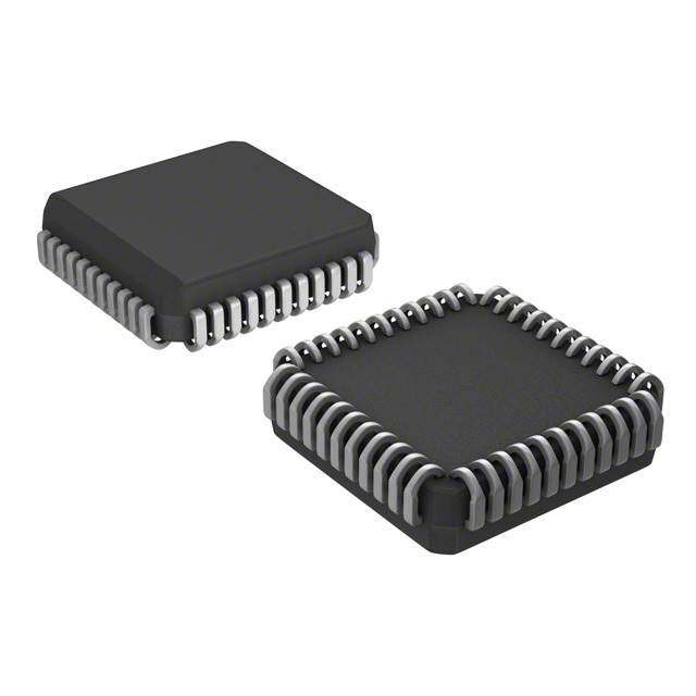
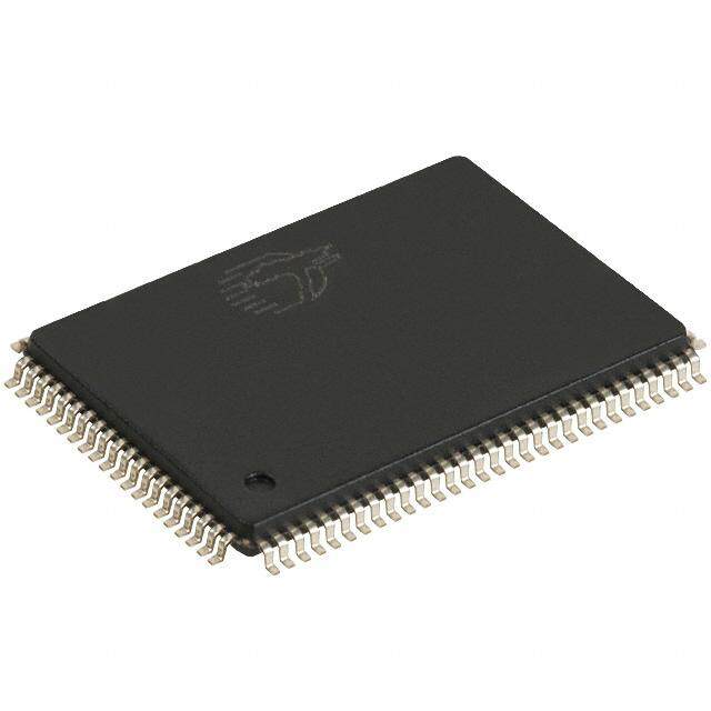
| 描述 | IC DUAL UART 64BYTE FIFO 44-PLCCUART 接口集成电路 1.8V to 5V Dual UART |
| 产品分类 | |
| FIFO | 64 字节 |
| 品牌 | Texas Instruments |
| 产品手册 | |
| 产品图片 |
|
| rohs | 符合RoHS无铅 / 符合限制有害物质指令(RoHS)规范要求 |
| 产品系列 | 接口 IC,UART 接口集成电路,Texas Instruments TL16C2752FN- |
| 数据手册 | |
| 产品型号 | TL16C2752FN |
| 产品目录页面 | |
| 产品种类 | UART 接口集成电路 |
| 供应商器件封装 | 44-PLCC(16.58x16.58) |
| 其它名称 | 296-21988-5 |
| 包装 | 管件 |
| 协议 | RS485 |
| 单位重量 | 2.266 g |
| 商标 | Texas Instruments |
| 安装类型 | 表面贴装 |
| 安装风格 | SMD/SMT |
| 封装 | Tube |
| 封装/外壳 | 44-LCC(J 形引线) |
| 封装/箱体 | PLCC-44 |
| 工作电源电压 | 5 V |
| 工厂包装数量 | 26 |
| 带CMOS | - |
| 带IrDA编码器/解码器 | - |
| 带假起始位检测 | 是 |
| 带并行端口 | - |
| 带自动流量控制 | 是 |
| 带调制解调器控制 | 是 |
| 数据速率 | 3 Mbps |
| 最大工作温度 | + 70 C |
| 最小工作温度 | 0 C |
| 标准包装 | 26 |
| 特性 | 故障启动位检测 |
| 电压-电源 | 1.8V,2.5V,3.3V,5V |
| 电源电压-最大 | 5.5 V |
| 电源电压-最小 | 4.5 V |
| 类型 | IrDA or RS-485 |
| 系列 | TL16C2752 |
| 通道数 | 2,DUART |
| 通道数量 | 2 Channel |


.jpg)


- 商务部:美国ITC正式对集成电路等产品启动337调查
- 曝三星4nm工艺存在良率问题 高通将骁龙8 Gen1或转产台积电
- 太阳诱电将投资9.5亿元在常州建新厂生产MLCC 预计2023年完工
- 英特尔发布欧洲新工厂建设计划 深化IDM 2.0 战略
- 台积电先进制程称霸业界 有大客户加持明年业绩稳了
- 达到5530亿美元!SIA预计今年全球半导体销售额将创下新高
- 英特尔拟将自动驾驶子公司Mobileye上市 估值或超500亿美元
- 三星加码芯片和SET,合并消费电子和移动部门,撤换高东真等 CEO
- 三星电子宣布重大人事变动 还合并消费电子和移动部门
- 海关总署:前11个月进口集成电路产品价值2.52万亿元 增长14.8%


PDF Datasheet 数据手册内容提取
TL16C2752 www.ti.com................................................................................................................................................ SLWS188A–JUNE2006–REVISEDSEPTEMBER2008 1.8-V to 5-V DUAL UART WITH 64-BYTE FIFOS FEATURES 1 • LargerFIFOsReduceCPUOverhead • FullyProgrammableSerialInterface • ProgrammableAuto-RTSandAuto-CTS Characteristics • InAuto-CTSMode,CTSControlsthe – 5-,6-,7-,or8-BitCharacters Transmitter – Even-,Odd-,orNo-ParityBitGeneration • InAuto-RTSMode,RCVFIFOContents,and andDetection ThresholdControlRTS – 1-,1=-,or2-StopBitGeneration • SerialandModemControlOutputsDrivea – BaudGeneration(DCto1Mbit/s) RJ11CableDirectlyWhenEquipmentisonthe • False-StartBitDetection SamePowerDrop • CompleteStatusReportingCapabilities • CapableofRunningWithAllExisting • 3-StateOutputTTLDriveCapabilitiesfor TL16C450Software BidirectionalDataBusandControlBus • AfterReset,AllRegistersAreIdenticaltothe • LineBreakGenerationandDetection TL16C450RegisterSet • InternalDiagnosticCapabilities • Upto48-MHzClockRateforupto3-Mbps – LoopbackControlsforCommunications (Standard16×Sampling)Operation,orupto LinkFaultIsolation 6-Mbps(Optional8×Sampling)OperationWith V =5VNominal – Break,Parity,Overrun,andFramingError CC • Upto32-MHzClockRateforupto2-Mbps Simulation (Standard16×Sampling)Operation,orupto • FullyPrioritizedInterruptSystemControls 4-Mbps(Optional8×Sampling)OperationWith • ModemControlFunctions(CTS,RTS,DSR, V =3.3VNominal DTR,RI,andDCD) CC • Upto24-MHzClockRateforupto1.5-Mbps • Availablein44-PinPLCC(FN)or32-PinQFN (Standard16×Sampling)Operation,orupto (RHB)Packages 3-Mbps(Optional8×Sampling)OperationWith • EachUART'sInternalRegisterSetMayBe VCC=2.5VNominal WrittenConcurrentlytoSaveSetupTime • Upto16-MHzClockRateforupto1-Mbps • Multifunction(MF)OutputAllowsUsersto (Standard16×Sampling)Operation,orupto SelectAmongSeveralFunctions,Saving 2-Mbps(Optional8×Sampling)OperationWith PackagePins V =1.8VNominal CC • InTL16C450Mode,HoldandShiftRegisters APPLICATIONS EliminatetheNeedforPrecise • Point-of-SaleTerminals SynchronizationBetweentheCPUandSerial • GamingTerminals Data • PortableApplications • ProgrammableBaud-RateGeneratorAllows • RouterControl DivisionofAnyInputReferenceClockby1to • CellularData (216–1)andGeneratesanInternal16×Clock • FactoryAutomation • StandardAsynchronousCommunicationBits (Start,Stop,andParity)AddedtoorDeleted FromtheSerialDataStream • 5-V,3.3-V,2.5-V,and1.8-VOperation • IndependentReceiverClockInput • Transmit,Receive,LineStatus,andDataSet InterruptsIndependentlyControlled 1 Pleasebeawarethatanimportantnoticeconcerningavailability,standardwarranty,anduseincriticalapplicationsofTexas Instrumentssemiconductorproductsanddisclaimerstheretoappearsattheendofthisdatasheet. PRODUCTIONDATAinformationiscurrentasofpublicationdate. Copyright©2006–2008,TexasInstrumentsIncorporated Products conform to specifications per the terms of the Texas Instruments standard warranty. Production processing does not necessarilyincludetestingofallparameters.
TL16C2752 SLWS188A–JUNE2006–REVISEDSEPTEMBER2008................................................................................................................................................ www.ti.com DESCRIPTION The TL16C2752 is a speed and functional upgrade of the TL16C2552. Since they are pinout and software compatible, designs can easily migrate from the TL16C2552 to the TL16C2752 if needed. The additional functionality within the TL16C2752 is accessed via an extended register set. Some of the key new features are larger receive and transmit FIFOs, embedded IrDA encoders and decoders, RS-485 transceiver controls, software flow control (Xon/Xoff) modes, programmable transmit FIFO thresholds, extended receive and transmit thresholdlevelsforinterrupts,andextendedreceivethresholdlevelsforflowcontrolhalt/resumeoperation. The TL16C2752 is a dual universal asynchronous receiver and transmitter (UART). It incorporates the functionality of two independent UARTs: each UART having its own register set and transmit and receive FIFOs. The two UARTs share only the data bus interface and clock source, otherwise they operate independently. Another name for the UART function is asynchronous communications element (ACE), and these terms will be used interchangeably. The bulk of this document describes the behavior of each ACE, with the understanding thattwosuchdevicesareincorporatedintotheTL16C2752. Functionally equivalent to the TL16C450 on power up or reset (single character or TL16C450 mode), each ACE can be placed in an alternate FIFO mode. This relieves the CPU of excessive software overhead by buffering received and to-be-transmitted characters. Each receiver and transmitter store up to 64 bytes in their respective FIFOs, with the receive FIFO including three additional bits per byte for error status. In the FIFO mode, selectable hardware or software autoflow control features can significantly reduce program overload and increasesystemefficiencybyautomaticallycontrollingserialdataflow. Each ACE performs serial-to-parallel conversions on data received from a peripheral device or modem and stores the parallel data in its receive buffer or FIFO, and each ACE performs parallel-to-serial conversions on data sent from its CPU after storing the parallel data in its transmit buffer or FIFO. The CPU can read the status of either ACE at any time. Each ACE includes complete modem control capability and a processor interrupt systemthatcanbetailoredtotheapplication. Each ACE includes a programmable baud rate generator capable of dividing a reference clock with divisors of from 1 to 65535, thus producing a 16× or 8× internal reference clock for the transmitter and receiver logic. Each ACE accommodates up to a 3-Mbaud serial data rate (48-MHz input clock). As a reference point, that speed would generate a 333-ns bit time and a 3.33-=s character time (for 8,N,1 serial data), with the internal clock runningat48MHzand16×sampling. EachACEhasaTXRDYandRXRDY(viaMF)outputthatcanbeusedtointerfacetoaDMAcontroller. 2 SubmitDocumentationFeedback Copyright©2006–2008,TexasInstrumentsIncorporated ProductFolderLink(s):TL16C2752
TL16C2752 www.ti.com................................................................................................................................................ SLWS188A–JUNE2006–REVISEDSEPTEMBER2008 TL16C2752 Block Diagram UART Channel A A2−A0 TXA Tx 64-Byte TX FIFO D7−D0 IR ENC CTSA CS DTRA CHSEL UART Registers DSRA, RIA, CDA IOR Baud- RTSA Rate Rx IOW Gen 64-Byte RX FIFO IR DEC RXA INTA Data Bus INTB Interface UART Channel B TXRDYA TXB Tx TXRDYB 64-Byte TX FIFO IR ENC CTSB MFA DTRB MFB UART Registers DSRB, RIB, CDB Baud- RTSB RESET Rate Rx Gen 64-Byte RX FIFO IR DEC RXB Crystal XTAL1 OSC XTAL2 Buffer VCC GND A. MFoutputallowsselectionofOP,BAUDOUT,orRXRDYperchannel. Copyright©2006–2008,TexasInstrumentsIncorporated SubmitDocumentationFeedback 3 ProductFolderLink(s):TL16C2752
TL16C2752 SLWS188A–JUNE2006–REVISEDSEPTEMBER2008................................................................................................................................................ www.ti.com TERMINALFUNCTIONS TERMINAL I/O DESCRIPTION NAME FNNO. RHBNO. A0 10 3 I Address0selectbit.Internalregistersaddressselection. A1 14 6 I Address1selectbit.Internalregistersaddressselection. A2 15 7 I Address2selectbit.Internalregistersaddressselection. Carrierdetect(activelow).TheseinputsareassociatedwithindividualUARTchannelsAand CDA, 42, B.Alowonthesepinsindicatesthatacarrierhasbeendetectedbythemodemforthat – I CDB 30 channel.Thestateoftheseinputsisreflectedinthemodemstatusregister(MSR).These inputsshouldbepulledhighifunused. Channelselect.UARTchannelAorBisselectedbythestateofthispinwhenCSisalogic0. Alogic0ontheCHSELselectstheUARTchannelB,whilealogic1selectsUARTchannelA. CHSELcouldjustbeanaddresslinefromtheuserCPUsuchasA3.Bit0ofthealternate CHSEL 16 8 I functionregister(AFR)cantemporarilyoverrideCHSELfunction,allowingtheusertowriteto bothchannelregistersimultaneouslywithonewritecyclewhenCSislow.Itisespecially usefulduringtheinitializationroutine. UARTchipselect(activelow).ThispinselectschannelAorBinaccordancewiththestateof CS 18 10 I theCHSELpin.ThisallowsdatatobetransferredbetweentheuserCPUandtheTL16C2752. Cleartosend(activelow).TheseinputsareassociatedwithindividualUARTchannelsAand B.AlogiclowontheCTSpinsindicatesthemodemordatasetisreadytoaccepttransmit CTSA, 40, 25, datafromtheTL16C2752.StatuscanbetestedbyreadingMSRbit4.Thesepinsonlyaffect I CTSB 28 17 thetransmitandreceiveoperationswhenautoCTSfunctionisenabledthroughtheenhanced featureregister(EFR)bit7,forhardwareflowcontroloperation.Theseinputsshouldbepulled highifunused. D0–D4 2–6 27–31 Databus(bidirectional).Thesepinsarethe8-bit,3-statedatabusfortransferringinformation I/O toorfromthecontrollingCPU.D0istheleastsignificantbit(LSB)andthefirstdatabitina D5–D7 7–9 32,1,2 transmitorreceiveserialdatastream. Datasetready(activelow).TheseinputsareassociatedwithindividualUARTchannelsAand DSRA, 41, B.Alogiclowonthesepinsindicatesthemodemordatasetispoweredonandisreadyfor – I DSRB 29 dataexchangewiththeUART.Thestateoftheseinputsisreflectedinthemodemstatus register(MSR).Theseinputsshouldbepulledhighifunused. Dataterminalready(activelow).TheseoutputsareassociatedwithindividualUARTchannels AandB.AlogiclowonthesepinsindicatesthattheTL16C2752ispoweredonandready. DTRA, 37, – O Thesepinscanbecontrolledthroughthemodemcontrolregister.Writinga1toMCRbit0 DTRB 27 setstheDTRoutputtolow,enablingthemodem.Theoutputofthesepinsishighafterwriting a0toMCRbit0,orafterareset. GND 12,22 20 Signalandpowerground InterruptAandB(activehigh).Thesepinsprovideindividualchannelinterrupts,INTAand INTB.INTAandINTBareenabledwhenMCRbit3issettoalogic1,interruptsourcesare INTA, 34, 21, O enabledintheinterruptenableregister(IER).Interruptconditionsincludereceivererrors, INTB 17 9 availablereceiverbufferdata,availabletransmitbufferspace,orwhenamodemstatusflagis detected.INTAandINTBareinthehigh-impedancestateafterreset. Readinput(active-lowstrobe).Ahigh-to-lowtransitiononIORloadsthecontentsofan IOR 24 14 I internalregisterdefinedbyaddressbitsA0–A2ontotheTL16C2752databus(D0–D7)for accessbyanexternalCPU. Writeinput(active-lowstrobe).Alow-to-hightransitiononIOWtransfersthecontentsofthe IOW 20 11 I databus(D0–D7)fromtheexternalCPUtoaninternalregisterthatisdefinedbyaddressbits A0–A2andCSAandCSB. NC – 18,19 Nointernalconnection Multifunction.ThisoutputpincanfunctionastheOP,BAUDOUT,orRXRDYpin.Oneofthese outputsignalfunctionscanbeselectedbytheuser-programmablebits1–2ofthealternate functionregister(AFR).Thesesignalfunctionsaredescribedasfollows: 1. OP–WhenOP(activelow)isselected,theMFpinisalogic0whenMCRbit3issettoa MFA, 35, logic 1 (see MCR bit 3). MCR bit 3 defaults to a logic 1 condition after a reset or MFB 19 – O powerup. 2. BAUDOUT–When BAUDOUT function is selected, the 16× baud rate clock output is availableatthispin. 3. RXRDY–RXRDY(activelow)isintendedformonitoringDMAdatatransfers. Ifitisnotused,leaveitunconnected. 4 SubmitDocumentationFeedback Copyright©2006–2008,TexasInstrumentsIncorporated ProductFolderLink(s):TL16C2752
TL16C2752 www.ti.com................................................................................................................................................ SLWS188A–JUNE2006–REVISEDSEPTEMBER2008 TERMINALFUNCTIONS(continued) TERMINAL I/O DESCRIPTION NAME FNNO. RHBNO. Reset.RESETwillresettheinternalregistersandalltheoutputs.TheUARTtransmitter RESET 21 12 I outputandthereceiverinputaredisabledduringresettime.SeeTL16C2752externalreset conditionsforinitializationdetails.RESETisanactive-highinput. Ringindicator(activelow).TheseinputsareassociatedwithindividualUARTchannelsAand B.Alogiclowonthesepinsindicatesthemodemhasreceivedaringingsignalfromthe RIA, 43, – I telephoneline.Alow-to-hightransitionontheseinputpinsgeneratesamodemstatus RIB 31 interrupt,ifenabled.Thestateoftheseinputsisreflectedinthemodemstatusregister(MSR). Theseinputsshouldbepulledhighifunused. Requesttosend(activelow).TheseoutputsareassociatedwithindividualUARTchannelsA andB.AlowontheRTSpinindicatesthetransmitterhasdatareadyandwaitingtosend. RTSA, 36, 22, Writinga1inthemodemcontrolregister(MCRbit1)setsthesepinstolow,indicatingdatais O RTSB 23 13 available.Afterareset,thesepinsaresettohigh.Thesepinsonlyaffectsthetransmitand receiveoperationwhenautoRTSfunctionisenabledthroughtheenhancedfeatureregister (EFR)bit6,forhardwareflowcontroloperation. Receivedatainput.Theseinputsareassociatedwithindividualserialchanneldatatothe RXA, 39, 24, I TL16C2752.Duringthelocalloopbackmode,theseRXinputpinsaredisabledandTXdatais RXB 25 15 internallyconnectedtotheUARTRXinputinternally. Transmitdata.Theseoutputsareassociatedwithindividualserialtransmitchanneldatafrom TXA, 38, 23, O theTL16C2752.Duringthelocalloopbackmode,theTXinputpinisdisabledandTXdatais TXB 26 16 internallyconnectedtotheUARTRXinput. TXRDYA, 1, Transmitready(activelow).TXRDYAandBgolowwhenthereareatleastatrigger-level – O TXRDYB 32 numberofspacesavailable.TheygohighwhentheTXbufferisfull. V 33,44 26 I Power-supplyinputs CC Crystalorexternalclock.XTAL1functionsasacrystalinputorasanexternalclockinput.A crystalcanbeconnectedbetweenXTAL1andXTAL2toformaninternaloscillatorcircuit(see XTAL1 11 4 I Figure4).Alternatively,anexternalclockcanbeconnectedtoXTAL1toprovidecustomdata rates. Crystaloscillatororbufferedclock(seealsoXTAL1).XTAL2isusedasacrystaloscillator XTAL2 13 5 O outputorbufferedaclockoutput. Detailed Description HardwareAutoflowControl(seeFigure1) Hardware autoflow control is comprised of auto-CTS and auto-RTS. With auto-CTS, the CTS input must be active before the transmitter FIFO can emit data. With auto-RTS, RTS becomes active when the receiver needs more data and notifies the sending serial device. When RTS is connected to CTS, data transmission does not occur unless the receiver FIFO has space for the data; thus, overrun errors are eliminated using ACE1 and ACE2 from a TLC16C2752 with the autoflow control enabled. If not, overrun errors can occur when the transmit datarateexceedsthereceiverFIFOreadlatency. ACE1 ACE2 Serial to RX TX Parallel Parallel to Serial RCV XMT FIFO FIFO RTS CTS Flow Flow Control Control D7−D0 D7−D0 Parallel TX RX Serial to to Serial Parallel XMT RCV FIFO FIFO CTS RTS Flow Flow Control Control Figure1.AutoflowControl(Auto-RTSandAuto-CTS)Example Copyright©2006–2008,TexasInstrumentsIncorporated SubmitDocumentationFeedback 5 ProductFolderLink(s):TL16C2752
TL16C2752 SLWS188A–JUNE2006–REVISEDSEPTEMBER2008................................................................................................................................................ www.ti.com Auto-RTS Auto-RTS data flow control originates in the receiver timing and control block (see Figure 4) and is linked to the programmed receiver FIFO trigger level. When the receiver FIFO level reaches the defined halt trigger level 8 (see Figure 3), RTS is deasserted. The sending ACE may send an additional byte after the trigger level is reached (assuming the sending ACE has another byte to send) because it may not recognize the deassertion of RTS until after it has begun sending the additional byte. RTS is automatically reasserted once the defined resumetriggerlevelisreached. Auto-CTS The transmitter circuitry checks CTS before sending the next data byte. When CTS is active, it sends the next byte. To stop the transmitter from sending the following byte, CTS must be released before the middle of the last stop bit that is currently being sent (see Figure 2). The auto-CTS function reduces interrupts to the host system. When flow control is enabled, CTS level changes do not trigger host interrupts because the device automatically controlsitsowntransmitter.Withoutauto-CTS,the transmitter sends any data present in the transmit FIFO and a receiveroverrunerrormayresult. Auto-RTS and Auto-CTS Functional Timing SIN Start Byte N Stop Start Byte N+1 Stop Start Byte Stop RTS RD (RD RBR) 1 2 N N+1 Figure2.RTSFunctionalTimingWaveforms SOUT Start Bits 0−7 Stop Start Bits 0−7 Stop Start Bits 0−7 Stop CTS Figure3.CTSFunctionalTimingWaveforms A. Pinnumbersshownarefor44-pinPLCCFNpackage. Figure4.FunctionalBlockDiagram 6 SubmitDocumentationFeedback Copyright©2006–2008,TexasInstrumentsIncorporated ProductFolderLink(s):TL16C2752
TL16C2752 www.ti.com................................................................................................................................................ SLWS188A–JUNE2006–REVISEDSEPTEMBER2008 ABSOLUTE MAXIMUM RATINGS(1) overoperatingfree-airtemperaturerange(unlessotherwisenoted) MIN MAX UNIT V Supplyvoltagerange(2) –0.5 7 V CC V Inputvoltagerangeatanyinput –0.5 7 V I V Outputvoltagerange –0.5 7 V O TL16C2752 0 70 T Operatingfree-airtemperaturerange °C A TL16C2752I –40 85 T Storagetemperaturerange –65 150 °C stg Leadtemperature1,6mm(1/16inch)fromcasefor10s 260 °C (1) Stressesbeyondthoselistedunder"absolutemaximumratings"maycausepermanentdamagetothedevice.Thesearestressratings only,andfunctionaloperationofthedeviceattheseoranyotherconditionsbeyondthoseindicatedunder"recommendedoperating conditions"isnotimplied.Exposuretoabsolute-maximum-ratedconditionsforextendedperiodsmayaffectdevicereliability. (2) AllvoltagevaluesarewithrespecttoV . SS RECOMMENDED OPERATING CONDITIONS 1.8 V =10% overoperatingfree-airtemperaturerange(unlessotherwisenoted) MIN NOM MAX UNIT V Supplyvoltage 1.62 1.8 1.98 V CC V Inputvoltage 0 V V I CC V High-levelinputvoltage 1.4 1.98 V IH V Low-levelinputvoltage –0.3 0.4 V IL V Outputvoltage 0 V V O CC I High-leveloutputcurrent(alloutputs) 0.5 mA OH I Low-leveloutputcurrent(alloutputs) 1 mA OL Oscillator/clockspeed 10 MHz RECOMMENDED OPERATING CONDITIONS 2.5 V =10% overoperatingfree-airtemperaturerange(unlessotherwisenoted) MIN NOM MAX UNIT V Supplyvoltage 2.25 2.5 2.75 V CC V Inputvoltage 0 V V I CC V High-levelinputvoltage 1.8 2.75 V IH V Low-levelinputvoltage –0.3 0.6 V IL V Outputvoltage 0 V V O CC I High-leveloutputcurrent(alloutputs) 1 mA OH I Low-leveloutputcurrent(alloutputs) 2 mA OL Oscillator/clockspeed 16 MHz Copyright©2006–2008,TexasInstrumentsIncorporated SubmitDocumentationFeedback 7 ProductFolderLink(s):TL16C2752
TL16C2752 SLWS188A–JUNE2006–REVISEDSEPTEMBER2008................................................................................................................................................ www.ti.com RECOMMENDED OPERATING CONDITIONS 3.3 V =10% overoperatingfree-airtemperaturerange(unlessotherwisenoted) MIN NOM MAX UNIT V Supplyvoltage 3 3.3 3.6 V CC V Inputvoltage 0 V V I CC V High-levelinputvoltage 0.7×V V IH CC V Low-levelinputvoltage 0.3×V V IL CC V Outputvoltage 0 V V O CC I High-leveloutputcurrent(alloutputs) 1.8 mA OH I Low-leveloutputcurrent(alloutputs) 3.2 mA OL Oscillator/clockspeed 20 MHz RECOMMENDED OPERATING CONDITIONS 5 V =10% overoperatingfree-airtemperaturerange(unlessotherwisenoted) MIN NOM MAX UNIT V Supplyvoltage 4.5 5 5.5 V CC V Inputvoltage 0 V V I CC AllexceptXTAL1,XTAL2 2 V High-levelinputvoltage V IH XTAL1,XTAL2 0.7×V CC AllexceptXTAL1,XTAL2 0.8 V Low-levelinputvoltage V IL XTAL1,XTAL2 0.3×V CC V Outputvoltage 0 V V O CC I High-leveloutputcurrent(alloutputs) 4 mA OH I Low-leveloutputcurrent(alloutputs) 4 mA OL Oscillator/clockspeed 24 MHz ELECTRICAL CHARACTERISTICS 1.8 V Nominal overrecommendedrangesofsupplyvoltageandoperatingfree-airtemperature(unlessotherwisenoted) PARAMETER TESTCONDITIONS MIN TYP(1) MAX UNIT V High-leveloutputvoltage(2) I =–0.5mA 1.3 V OH OH V Low-leveloutputvoltage(2) I =1mA 0.5 V OL OL V =1.98V,V =0,V =0to1.98V, I Inputcurrent CC SS I 10 =A I Allotherterminalsfloating High-impedance-state V =1.98V,V =0,V =0to1.98V, I CC SS I ±20 =A OZ outputcurrent Chipselectedinwritemodeorchipdeselected V =1.98V,T =0°C,RXA,RXB,DSRA,DSRB,CDA, CC A I Supplycurrent CDB,CTSA,CTSB,RIA,andRIBat1.4V,Allotherinputsat mA CC 0.4V,XTAL1at16MHz,Noloadonoutputs C Clockinputimpedance 15 20 pF i(CLK) V =0,V =0,f=1MHz, C Clockoutputimpedance CC SS 20 30 pF O(CLK) T =25°C,Allotherterminalsgrounded A C Inputimpedance 6 10 pF I C Outputimpedance 10 20 pF O (1) AlltypicalvaluesareatV =1.8VandT =25°C. CC A (2) TheseparametersapplyforalloutputsexceptXTAL2. 8 SubmitDocumentationFeedback Copyright©2006–2008,TexasInstrumentsIncorporated ProductFolderLink(s):TL16C2752
TL16C2752 www.ti.com................................................................................................................................................ SLWS188A–JUNE2006–REVISEDSEPTEMBER2008 ELECTRICAL CHARACTERISTICS 2.5 V Nominal overrecommendedrangesofsupplyvoltageandoperatingfree-airtemperature(unlessotherwisenoted) PARAMETER TESTCONDITIONS MIN TYP(1) MAX UNIT V High-leveloutputvoltage(2) I =–1mA 1.8 V OH OH V Low-leveloutputvoltage(2) I =2mA 0.5 V OL OL V =2.75V,V =0,V =0to2.75V, I Inputcurrent CC SS I 10 =A I Allotherterminalsfloating High-impedance-state V =2.75V,V =0,V =0to2.75V, I CC SS I ±20 =A OZ outputcurrent Chipselectedinwritemodeorchipdeselected V =2.75V,T =0°C,RXA,RXB,DSRA,DSRB,CDA, CC A I Supplycurrent CDB,CTSA,CTSB,RIA,andRIBat1.8V,Allother mA CC inputsat0.6V,XTAL1at24MHz,Noloadonoutputs C Clockinputimpedance 15 20 pF i(CLK) V =0,V =0,f=1MHz, C Clockoutputimpedance CC SS 20 30 pF O(CLK) T =25°C,Allotherterminalsgrounded A C Inputimpedance 6 10 pF I C Outputimpedance 10 20 pF O (1) AlltypicalvaluesareatV =2.5VandT =25°C. CC A (2) TheseparametersapplyforalloutputsexceptXTAL2. ELECTRICAL CHARACTERISTICS 3.3 V Nominal overrecommendedrangesofsupplyvoltageandoperatingfree-airtemperature(unlessotherwisenoted) PARAMETER TESTCONDITIONS MIN TYP(1) MAX UNIT V High-leveloutputvoltage(2) I =–1.8mA 2.4 V OH OH V Low-leveloutputvoltage(2) I =3.2mA 0.5 V OL OL V =3.6V,V =0,V =0to3.6V, I Inputcurrent CC SS I 10 =A I Allotherterminalsfloating High-impedance-state V =3.6V,V =0,V =0to3.6V, I CC SS I ±20 =A OZ outputcurrent Chipselectedinwritemodeorchipdeselected V =3.6V,T =0°C,RXA,RXB,DSRA,DSRB,CDA, CC A I Supplycurrent CDB,CTSA,CTSB,RIA,andRIBat2V,Allotherinputs mA CC at0.8V,XTAL1at32MHz,Noloadonoutputs C Clockinputimpedance 15 20 pF i(CLK) V =0,V =0,f=1MHz, C Clockoutputimpedance CC SS 20 30 pF O(CLK) T =25°C,Allotherterminalsgrounded A C Inputimpedance 6 10 pF I C Outputimpedance 10 20 pF O (1) AlltypicalvaluesareatV =3.3VandT =25°C. CC A (2) TheseparametersapplyforalloutputsexceptXTAL2. Copyright©2006–2008,TexasInstrumentsIncorporated SubmitDocumentationFeedback 9 ProductFolderLink(s):TL16C2752
TL16C2752 SLWS188A–JUNE2006–REVISEDSEPTEMBER2008................................................................................................................................................ www.ti.com ELECTRICAL CHARACTERISTICS 5 V Nominal overrecommendedrangesofsupplyvoltageandoperatingfree-airtemperature(unlessotherwisenoted) PARAMETER TESTCONDITIONS MIN TYP(1) MAX UNIT V High-leveloutputvoltage(2) I =–4mA 4 V OH OH V Low-leveloutputvoltage(2) I =4mA 0.4 V OL OL V =5.5V,V =0,V =0to5.5V, I Inputcurrent CC SS I 10 =A I Allotherterminalsfloating High-impedance-state V =3.6V,V =0,V =0to3.6V, I CC SS I =20 =A OZ outputcurrent Chipselectedinwritemodeorchipdeselected V =5.5V,T =0°C,RXA,RXB,DSRA,DSRB,CDA, CC A CDB,CTSA,CTSB,RIA,andRIBat2V, I Supplycurrent mA CC Allotherinputsat0.8V,XTAL1at32MHz, Noloadonoutputs C Clockinputimpedance 15 20 pF i(CLK) V =0,V =0,f=1MHz, C Clockoutputimpedance CC SS 20 30 pF O(CLK) T =25°C,Allotherterminalsgrounded A C Inputimpedance 6 10 pF I C Outputimpedance 10 20 pF O (1) AlltypicalvaluesareatV =3.3VandT =25°C. CC A (2) TheseparametersapplyforalloutputsexceptXTAL2. TIMING REQUIREMENTS overrecommendedrangesofsupplyvoltageandoperatingfree-airtemperature(unlessotherwisenoted) LIMITS ALT. TEST PARAMETER FIGURE 1.8V 2.5V 3.3V 5V UNIT SYMBOL CONDITIONS MIN MAX MIN MAX MIN MAX MIN MAX tw8 Pulseduration,RESET tRESET 1 1 1 1 =s tw1 Pulseduration,clockhigh tXH 6 25 16 12 8 ns tw2 Pulseduration,clocklow tXL tcR Cycletime,read(tw7+td8+th7) RC 8 115 80 62 57 ns tcW Cycletime,write(tw6+td5+th4) WC 7 115 80 62 57 ns tw6 Pulseduration,IOWorCS tIOW 7 80 55 45 40 ns tw7 Pulseduration,IORorCS tIOR 8 80 55 45 40 ns Setuptime,datavalidbeforeIOW↑ tSU3 orCS↑ tDS 7 25 20 15 15 ns Holdtime,addressvalidafterIOW↑ th4 orCS↑ tWA 7 20 15 10 10 ns Holdtime,datavalidafterIOW↑or th5 CS↑ tDH 7 15 10 5 5 ns Holdtime,datavalidafterIOR↑or th7 CS↑ tRA 8 20 15 10 10 ns Delaytime,addressvalidbefore td5 IOW↓orCS↓ tAW 7 15 10 7 7 ns Delaytime,addressvalidtoIOR↓or td8 CS↓ tAR 8 15 10 7 7 ns Delaytime,IOR↓orCS↓todata td10 valid tRVD 8 CL=30pF 55 35 25 20 ns Delaytime,IOR↑orCS↑tofloating td11 data tHZ 8 CL=30pF 40 30 20 20 ns td12 Writecycletowritecycledelay 7 100 75 60 50 ns td13 Readcycletoreadcycledelay 8 100 75 60 50 ns 10 SubmitDocumentationFeedback Copyright©2006–2008,TexasInstrumentsIncorporated ProductFolderLink(s):TL16C2752
TL16C2752 www.ti.com................................................................................................................................................ SLWS188A–JUNE2006–REVISEDSEPTEMBER2008 BAUD GENERATOR SWITCHING CHARACTERISTICS overrecommendedrangesofsupplyvoltageandoperatingfree-airtemperature,C =30pF(forFNpackageonly) L LIMITS TEST ALT. PARAMETER FIGURE CONDITION 1.8V 2.5V 3.3V 5V UNIT SYMBOL S MIN MAX MIN MAX MIN MAX MIN MAX tw3 Pulseduration,BAUDOUTlow tLW 6 CLK÷2 50 35 27 16 ns tw4 Pulseduration,BAUDOUThigh tHW 6 CLK÷2 50 35 27 16 ns td1 Delaytime,XIN↑toBAUDOUT↑ tBLD 6 35 25 20 15 ns td2 Delaytime,XIN↑↓toBAUDOUT↓ tBHD 6 35 25 20 15 ns RECEIVER SWITCHING CHARACTERISTICS(1) overrecommendedrangesofsupplyvoltageandoperatingfree-airtemperature(unlessotherwisenoted) LIMITS ALT. TEST PARAMETER FIGURE 1.8V 2.5V 3.3V 5V UNIT SYMBOL CONDITIONS MIN MAX MIN MAX MIN MAX MIN MAX td12 Delaytime,RCLKtosample tSCD 9 20 15 10 10 ns Delaytime,stoptosetINTor 8,9,10, RCLK td13 readRBRtoLSIinterruptorstop tSINT 11,12 1 1 1 1 cycle toRXRDY↓ Delaytime,readRBR/LSRto 8,9,10, td14 resetINT tRINT 11,12 CL=30pF 100 90 80 70 ns Delaytime,RCVthresholdbyte baudout td26 toRTS↑ 19 CL=30pF 2 cycles(2) Delaytime,readoflastbytein baudout td27 receiveFIFOtoRTS↓ 19 CL=30pF 2 cycles Delaytime,firstdatabitof16th baudout td28 charactertoRTS↑ 20 CL=30pF 2 cycles Delaytime,RBRRDlowtoRTS↓ baudout td29 20 CL=30pF 2 cycles (1) IntheFIFOmode,thereadcycle(RC)=1baudclock(min)betweenreadsofthereceiveFIFOandthestatusregisters(interrupt identificationregisterorlinestatusregister). (2) AbaudoutcycleisequaltotheperiodoftheinputclockdividedbytheprogrammeddividerinDLL,DLM. TRANSMITTER SWITCHING CHARACTERISTICS overrecommendedrangesofsupplyvoltageandoperatingfree-airtemperature(unlessotherwisenoted) LIMITS ALT. TEST PARAMETER FIGURE 1.8V 2.5V 3.3V 5V UNIT SYMBOL CONDITIONS MIN MAX MIN MAX MIN MAX MIN MAX Delaytime,initialwritetotransmit baudout td15 start tIRS 14 8 24 8 24 8 24 8 24 cycles baudout td16 Delaytime,starttoINT tSTI 14 8 10 8 10 8 10 8 10 cycles Delaytime,IOW(WRTHR)to td17 resetINT tHR 14 CL=30pF 70 60 50 50 ns Delaytime,initialwritetoINT baudout td18 (THRE(1)) tSI 14 16 34 16 34 16 34 16 34 cycles Delaytime,readIOR↑toresetINT td19 (THRE(1)) tIR 14 CL=30pF 70 50 35 35 ns Delaytime,writetoTXRDY td20 inactive tWXI 15,16 CL=30pF 60 45 35 35 ns baudout td21 Delaytime,starttoTXRDYactive tSXA 15,16 CL=30pF 9 9 9 9 cycles Setuptime,CTS↑beforemidpoint tSU4 ofstopbit 18 30 20 10 10 ns baudout td25 Delaytime,CTSlowtoTX↓ 18 CL=30pF 24 24 24 24 cycles (1) THRE=Transmitterholdingregisterempty;IIR=interruptidentificationregister Copyright©2006–2008,TexasInstrumentsIncorporated SubmitDocumentationFeedback 11 ProductFolderLink(s):TL16C2752
TL16C2752 SLWS188A–JUNE2006–REVISEDSEPTEMBER2008................................................................................................................................................ www.ti.com MODEM CONTROL SWITCHING CHARACTERISTICS overoperatingfree-airtemperaturerange(unlessotherwisenoted) LIMITS ALT. TEST PARAMETER FIGURE 1.8V 2.5V 3.3V 5V UNIT SYMBOL CONDITIONS MIN MAX MIN MAX MIN MAX MIN MAX td22 Delaytime,WRMCRtooutput tMDO 17 CL=30pF 90 70 60 50 ns Delaytime,modeminterruptto td23 setINT tSIM 17 CL=30pF 60 50 40 35 ns Delaytime,RDMSRtoreset td24 INT tRIM 17 CL=30pF 80 60 50 40 ns N tw1 tw2 XTAL td1 td2 MFA,B (1/1) td1 td2 MFA,B (1/2) tw3 tw4 MFA,B (1/3) MFA,B (1/N) (N > 3) 2 XIN Cycles (N−2) XIN Cycles Figure5.InputClockandBaudGeneratorTimingWaveforms (forFNPackageOnly)(WhenAFR2:1=01) 12 SubmitDocumentationFeedback Copyright©2006–2008,TexasInstrumentsIncorporated ProductFolderLink(s):TL16C2752
TL16C2752 www.ti.com................................................................................................................................................ SLWS188A–JUNE2006–REVISEDSEPTEMBER2008 CHSEL, Valid Address Valid Address A2−A0 td5 th4 td5 tw6 th4 tw6 CS td12 tw6 tw6 IOW tsu3 tsu3 th5 th5 D7−D0 Valid Data Valid Data Figure6.WriteCycleTimingWaveforms CHSEL, Valid Address Valid Address A2−A0 td8 th7 td8 tw7 th7 tw7 CS td13 tw7 tw7 IOR td10 td10 td11 th11 D7−D0 Valid Data Valid Data Figure7.ReadCycleTimingWaveforms Copyright©2006–2008,TexasInstrumentsIncorporated SubmitDocumentationFeedback 13 ProductFolderLink(s):TL16C2752
TL16C2752 SLWS188A–JUNE2006–REVISEDSEPTEMBER2008................................................................................................................................................ www.ti.com RCLK (Internal) td12 8 CLKs Sample Clock (Internal) TL16C450 Mode: RXA, RXB Start Data Bits 5−8 Parity Stop Sample Clock INT 50% 50% (data ready) td13 td14 INT 50% 50% (RCV error) IOR 50% Active (read RBR) IOR 50% Active (read LSR) td14 Figure8.ReceiverTimingWaveforms 14 SubmitDocumentationFeedback Copyright©2006–2008,TexasInstrumentsIncorporated ProductFolderLink(s):TL16C2752
TL16C2752 www.ti.com................................................................................................................................................ SLWS188A–JUNE2006–REVISEDSEPTEMBER2008 RXA, RXB Data Bits 5−8 Stop Sample Clock (Internal) (FIFO at or above Trigger Level trigger level) INT 50% 50% (FCR6, 7 = 0, 0) (FIFO below trigger level) td13 td14 (see Note A) INT 50% 50% Line Status Interrupt (LSI) td14 IOR Active (RD LSR) 50% Active IOR 50% (RD RBR) Figure9.ReceiveFIFOFirstByte(SetsDRBit)Waveforms RXA, RXB Stop Sample Clock (Internal) (FIFO at or above Time-Out or trigger level) Trigger Level 50% 50% Interrupt (FIFO below trigger level) td13 (see Note A) td14 Line Status 50% Top Byte of FIFO 50% Interrupt (LSI) td13 td14 IOP 50% (RD LSR) IOR Active 50% 50% Active (RD RBR) Previous Byte Read From FIFO Figure10.ReceiveFIFOBytesOtherThantheFirstByte(DRInternalBitAlreadySet)Waveforms Copyright©2006–2008,TexasInstrumentsIncorporated SubmitDocumentationFeedback 15 ProductFolderLink(s):TL16C2752
TL16C2752 SLWS188A–JUNE2006–REVISEDSEPTEMBER2008................................................................................................................................................ www.ti.com IOR 50% Active (RD RBR) See Note A RXA, RXB (first byte) Stop Sample Clock (Internal) td13 (see Note B) td14 50% 50% RXRDYA, RXRDYB Figure11.ReceiverReady(RXRDY)Waveforms,FCR0=0orFCR0=1andFCR3=0(Mode0) IOR (RD RBR) 50% Active RXA, RXB See Note A (first byte that reaches the trigger level) Sample Clock (Internal) td13 (see Note B) td14 RXRDYA, RXRDYB 50% 50% Figure12.ReceiverReady(RXRDY)Waveforms,FCR0=1andFCR3=1(Mode1) Start Start TXA, TXB 50% Data Bits Parity Stop 50% td15 td16 INT 50% 50% 50% 50% 50% (THRE) td18 td17 td17 IOW 50% 50% 50% (WR THR) td19 IOR 50% Figure13.TransmitterTimingWaveforms 16 SubmitDocumentationFeedback Copyright©2006–2008,TexasInstrumentsIncorporated ProductFolderLink(s):TL16C2752
TL16C2752 www.ti.com................................................................................................................................................ SLWS188A–JUNE2006–REVISEDSEPTEMBER2008 IOW Byte 1 50% (WR THR) Start TXA, TXB Data Parity Stop 50% td20 td21 TXRDYA, TXRDYB 50% 50% Figure14.TransmitterReady(TXRDY)Waveforms,FCR0=0orFCR0=1andFCR3=0(Mode0) IOW Byte 16 50% (WR THR) Start TXA, TXB Data Parity Stop 50% td20 td21 TXRDYA, TXRDYB 50% FIFO Full 50% Figure15.TransmitterReady(TXRDY)Waveforms,FCR0=1andFCR3=1(Mode1) IOW 50% 50% (WR MCR) td22 td22 RTSA, RTSB, DTRA, 50% 50% DTRB, OPA, OPB 50% CTSA, CTSB, DSRA, DSRB, CDA, CDB td23 INT 50% 50% 50% (modem) td24 IOR (RD MSR) 50% td23 RI 50% Figure16.ModemControlTimingWaveforms Copyright©2006–2008,TexasInstrumentsIncorporated SubmitDocumentationFeedback 17 ProductFolderLink(s):TL16C2752
TL16C2752 SLWS188A–JUNE2006–REVISEDSEPTEMBER2008................................................................................................................................................ www.ti.com tsu4 CTSA, CTSB 50% 50% td25 TXA, TXB 50% Midpoint of Stop Bit Figure17.CTSandTXAutoflowControlTiming(StartandStop)Waveforms Midpoint of Stop Bit RXA, RXB td26 td27 RTSA, 50% 50% RTSB IOR 50% Figure18.Auto-RTSTiming 18 SubmitDocumentationFeedback Copyright©2006–2008,TexasInstrumentsIncorporated ProductFolderLink(s):TL16C2752
TL16C2752 www.ti.com................................................................................................................................................ SLWS188A–JUNE2006–REVISEDSEPTEMBER2008 APPLICATION INFORMATION A. Pinnumbersshownarefor44-pinPLCCFNpackage. Figure19.TypicalTL16C2752Connection Copyright©2006–2008,TexasInstrumentsIncorporated SubmitDocumentationFeedback 19 ProductFolderLink(s):TL16C2752
TL16C2752 SLWS188A–JUNE2006–REVISEDSEPTEMBER2008................................................................................................................................................ www.ti.com PRINCIPLES OF OPERATION UART Internal Registers Each of the UART channel in the TL16C2752 has its own set of configuration registers selected by address lines A0, A1, and A2 with CS and CHSEL selecting the channel. The complete register set is shown in Table 1 and Table2. Table1.UARTChannelAandBUARTInternalRegisters ADDRESS RESET (HEX) COMMENTS REGISTER READ/WRITE A2–A0 VALUE 16C550CompatibleRegisters XX RHR–ReceiveHoldingRegister Readonly 000 LCR[7]=0 XX THR–TransmitHoldingRegister Writeonly 000 XX DLL–DivLatchLowByte Read/Write 001 XX LCR[7]=1,LCR≠0xBF DLM–DivLatchHighByte Read/Write 010 00 AFR–AlternateFunctionRegister Read/Write 000 00 DLL,DLM=0x00, DREV–DeviceRevisionCode Readonly 001 0A LCR[7]=1,LCR≠0xBF DVID–DeviceIdentificationCode Readonly 001 00 LCR[7]=0 IER–InterruptEnableRegister Read/Write 01 ISR–InterruptStatusRegister Readonly 010 LCR[7]=0 00 FCR–FIFOControlRegister Writeonly 011 00 LCR–LineControlRegister Read/Write 100 00 MCR–ModemControlRegister Read/Write LSR–LineStatusRegister Readonly 101 60 LCR≠0xBF Reserved Writeonly MSR–ModemStatusRegister Readonly 110 X0 Reserved Writeonly 111 FF LCR≠0xBF,FCTR[6]=0 SPR–ScratchPadRegister Read/Write 111 00 FLVL–RX/TXFIFOLevelCounterRegister Readonly LCR≠0xBF,FCTR[6]=1 111 80 EMSR–EnhancedModeSelectRegister Writeonly EnhancedRegisters 00 TRG–RX/TXFIFOTriggerLevelRegister Writeonly 000 00 FC–RX/TXFIFOLevelCounterRegister Readonly 001 00 FCTR–FeatureControlRegister Read/Write 010 00 EFR–EnhancedFunctionRegister Read/Write LCR=0xBF 100 00 Xon-1–XonCharacter1 Read/Write 101 00 Xon-2–XonCharacter2 Read/Write 110 00 Xoff-1–XoffCharacter1 Read/Write 111 00 Xoff-2–XoffCharacter2 Read/Write 20 SubmitDocumentationFeedback Copyright©2006–2008,TexasInstrumentsIncorporated ProductFolderLink(s):TL16C2752
TL16C2752 www.ti.com................................................................................................................................................ SLWS188A–JUNE2006–REVISEDSEPTEMBER2008 Table2.InternalRegistersDescription(1) Address Register Read/ Comments Bit7 Bit6 Bit5 Bit4 Bit3 Bit2 Bit1 Bit0 A2–A0 Name Write 16C550CompatibleRegisters 000 RHR RD LCR[7]=0 Bit7 Bit6 Bit5 Bit4 Bit3 Bit2 Bit1 Bit0 000 THR WR Bit7 Bit6 Bit5 Bit4 Bit3 Bit2 Bit1 Bit0 001 IER RD/WR 0/ 0/ 0/ 0/ ModemStat. RXLineStat. TXEmptyInt. RXDataInt. CTSInt. RTSInt. XoffInt. SleepMode Int.Enable Int.Enable Enable Enable Enable Enable Enable Enable 010 ISR RD 0/ 0/ FIFOs FIFOs INTSourceBit INTSourceBit INTSourceBit INTSourceBit Enabled Enabled INTSourceBit INTSource 3 2 1 0 5 Bit4 010 FCR WR 0/ 0/ RXFIFO RXFIFO DMAMode TXFIFO RXFIFO Trigger Trigger TXFIFO TXFIFO Enable Reset Reset FIFOsEnable Trigger Trigger Divisor WordLength WordLength 011 LCR RD/WR LCR≠0xBF SetTXBreak SetParity EvenParity ParityEnable StopBits Enable Bit1 Bit0 100 MCR RD/WR 0/ 0/ 0/ Internal OP2#Output RTS#Output DTR#Output BRG IRMode XonAny Loopback Control Rsrvd(OP1#) Control Control Prescaler Enable Enable RXFIFO THR&TSR RXFraming RXParity RXOverrun RXData 101 LSR RD THREmpty RXBreak GlobalError Empty Error Error Error Ready 110 MSR RD CD#Input RI#Input DSR#Input CTS#Input DeltaCD# DeltaRI# DeltaDSR# DeltaCTS# LCR≠0xBF Bit7 Bit6 Bit5 Bit4 Bit3 Bit2 Bit1 Bit0 111 SPR RD/WR FCTRBit6=0 16X LSRError AutoRS485 AutoRTS AutoRTS Rx/TxFIFO Rx/TxFIFo 111 EMSR WR LDR≠0xBF Sampling Interrupt Hyst.Bit3 HystBit2 Output Rsrvd Count Count FCTRBit6=1 RateMode Imd/Dly# Inversion 111 FLVL RD Bit7 Bit6 Bit5 Bit4 Bit3 Bit2 Bit1 Bit0 Baud-RateGeneratorDivisor 000 DLL RD/WR Bit7 Bit6 Bit5 Bit4 Bit3 Bit2 Bit1 Bit0 001 DLM RD/WR LCR[7]=1LCR Bit7 Bit6 Bit5 Bit4 Bit3 Bit2 Bit1 Bit0 ≠0xBF RXRDY# Baudout# Concurrent 010 AFR RD/WR Rsvd Rsvd Rsvd Rsvd Rsvd Select Select Write 000 DREV RD LCR[7]=1LCR Bit7 Bit6 Bit5 Bit4 Bit3 Bit2 Bit1 Bit0 ≠0xBFDLL= 001 DVID RD 0x00DLM= 0 0 0 0 1 0 1 0 0x00 EnhancedRegisters 000 TRG WR Bit7 Bit6 Bit5 Bit4 Bit3 Bit2 Bit1 Bit0 000 FC RD Bit7 Bit6 Bit5 Bit4 Bit3 Bit2 Bit1 Bit0 AutoRS485 RX/TX TrigTableBit TrigTable RXIRInput AutoRTS AutoRTS 001 FCTR RD/WR SCPADSwap Direction Mode 1 Bit0 Inv. HystBit1 HystBit0 Control Enable IER[7:4], 010 EFR RD/WR LCR=0xBF AutoCTS AutoRTS SpecialChar ISR[5:4], SoftwareFlow SoftwareFlow SoftwareFlow SoftwareFlow Enable Enable Select CntlBit3 CntlBit2 CntlBit1 CntlBit0 FCT[5:4], MCR[7:5] 100 XON1 RD/WR Bit7 Bit6 Bit5 Bit4 Bit3 Bit2 Bit1 Bit0 101 XON2 RD/WR Bit7 Bit6 Bit5 Bit4 Bit3 Bit2 Bit1 Bit0 110 XOFF1 RD/WR Bit7 Bit6 Bit5 Bit4 Bit3 Bit2 Bit1 Bit0 111 XOFF2 RD/WR Bit7 Bit6 Bit5 Bit4 Bit3 Bit2 Bit1 Bit0 (1) ShadedbitsareaccessiblewhenEFRBit4=1. Copyright©2006–2008,TexasInstrumentsIncorporated SubmitDocumentationFeedback 21 ProductFolderLink(s):TL16C2752
PACKAGE OPTION ADDENDUM www.ti.com 6-Feb-2020 PACKAGING INFORMATION Orderable Device Status Package Type Package Pins Package Eco Plan Lead/Ball Finish MSL Peak Temp Op Temp (°C) Device Marking Samples (1) Drawing Qty (2) (6) (3) (4/5) TL16C2752FN ACTIVE PLCC FN 44 26 Green (RoHS NIPDAU Level-3-260C-168 HR 0 to 70 2752FN & no Sb/Br) TL16C2752IFN ACTIVE PLCC FN 44 26 Green (RoHS NIPDAU Level-3-260C-168 HR -40 to 85 2752IFN & no Sb/Br) (1) The marketing status values are defined as follows: ACTIVE: Product device recommended for new designs. LIFEBUY: TI has announced that the device will be discontinued, and a lifetime-buy period is in effect. NRND: Not recommended for new designs. Device is in production to support existing customers, but TI does not recommend using this part in a new design. PREVIEW: Device has been announced but is not in production. Samples may or may not be available. OBSOLETE: TI has discontinued the production of the device. (2) RoHS: TI defines "RoHS" to mean semiconductor products that are compliant with the current EU RoHS requirements for all 10 RoHS substances, including the requirement that RoHS substance do not exceed 0.1% by weight in homogeneous materials. Where designed to be soldered at high temperatures, "RoHS" products are suitable for use in specified lead-free processes. TI may reference these types of products as "Pb-Free". RoHS Exempt: TI defines "RoHS Exempt" to mean products that contain lead but are compliant with EU RoHS pursuant to a specific EU RoHS exemption. Green: TI defines "Green" to mean the content of Chlorine (Cl) and Bromine (Br) based flame retardants meet JS709B low halogen requirements of <=1000ppm threshold. Antimony trioxide based flame retardants must also meet the <=1000ppm threshold requirement. (3) MSL, Peak Temp. - The Moisture Sensitivity Level rating according to the JEDEC industry standard classifications, and peak solder temperature. (4) There may be additional marking, which relates to the logo, the lot trace code information, or the environmental category on the device. (5) Multiple Device Markings will be inside parentheses. Only one Device Marking contained in parentheses and separated by a "~" will appear on a device. If a line is indented then it is a continuation of the previous line and the two combined represent the entire Device Marking for that device. (6) Lead/Ball Finish - Orderable Devices may have multiple material finish options. Finish options are separated by a vertical ruled line. Lead/Ball Finish values may wrap to two lines if the finish value exceeds the maximum column width. Important Information and Disclaimer:The information provided on this page represents TI's knowledge and belief as of the date that it is provided. TI bases its knowledge and belief on information provided by third parties, and makes no representation or warranty as to the accuracy of such information. Efforts are underway to better integrate information from third parties. TI has taken and continues to take reasonable steps to provide representative and accurate information but may not have conducted destructive testing or chemical analysis on incoming materials and chemicals. TI and TI suppliers consider certain information to be proprietary, and thus CAS numbers and other limited information may not be available for release. In no event shall TI's liability arising out of such information exceed the total purchase price of the TI part(s) at issue in this document sold by TI to Customer on an annual basis. Addendum-Page 1
PACKAGE OPTION ADDENDUM www.ti.com 6-Feb-2020 Addendum-Page 2
None
4215154/A 04/2017 PACKAGE OUTLINE FN0044A PLCC - 4.57 mm max height SCALE 0.800 PLASTIC CHIP CARRIER B .650-.656 .180 MAX [16.51-16.66] [4.57] .020 MIN NOTE 3 A [0.51] (.008) 6 1 44 40 [0.2] 7 39 PIN 1 ID .650-.656 (OPTIONAL) .582-.638 [16.51-16.66] [14.79-16.20] NOTE 3 17 29 18 28 .090-.120 TYP [2.29-3.04] 44X .026-.032 [0.66-0.81] C SEATING PLANE 44X .013-.021 .004 [0.1] C [0.33-0.53] 40X .050 [1.27] .007 [0.18] C A B .685-.695 [17.40-17.65] TYP 4215154/A 04/2017 NOTES: 1. All linear dimensions are in inches. Any dimensions in brackets are in millimeters. Any dimensions in parenthesis are for reference only. Controlling dimensions are in inches. Dimensioning and tolerancing per ASME Y14.5M. 2. This drawing is subject to change without notice. 3. Dimension does not include mold protrusion. Maximum allowable mold protrusion .01 in [0.25 mm] per side. 4. Reference JEDEC registration MS-018. www.ti.com
4215154/A 04/2017 EXAMPLE BOARD LAYOUT FN0044A PLCC - 4.57 mm max height PLASTIC CHIP CARRIER SYMM 44X (.093 ) [2.35] 6 1 44 40 7 39 44X (.030 ) [0.75] SYMM (.64 ) [16.2] 40X (.050 ) [1.27] 17 29 (R.002 ) TYP [0.05] 18 28 (.64 ) [16.2] LAND PATTERN EXAMPLE EXPOSED METAL SHOWN SCALE:4X .002 MAX EXPOSED METAL .002 MIN EXPOSED METAL [0.05] [0.05] ALL AROUND ALL AROUND METAL SOLDER MASK SOLDER MASK METAL UNDER OPENING OPENING SOLDER MASK NON SOLDER MASK SOLDER MASK DEFINED DEFINED (PREFERRED) SOLDER MASK DETAILS 4215154/A 04/2017 NOTES: (continued) 5. Publication IPC-7351 may have alternate designs. 6. Solder mask tolerances between and around signal pads can vary based on board fabrication site. www.ti.com
EXAMPLE STENCIL DESIGN FFNN00004444AA PPLLCCCC -- 44..5577 mmmm mmaaxx hheeiigghhtt PPLLAASSTTIICC CCHHIIPP CCAARRRRIIEERR SYMM 44X (.093 ) 6 1 44 40 [2.35] 7 39 44X (.030 ) [0.75] SYMM (.64 ) [16.2] 40X (.050 ) [1.27] 17 29 (R.002 ) TYP [0.05] 18 28 (.64 ) [16.2] SOLDER PASTE EXAMPLE BASED ON 0.125 mm THICK STENCIL SCALE:4X 4215154/A 04/2017 NOTES: (continued) 7. Laser cutting apertures with trapezoidal walls and rounded corners may offer better paste release. IPC-7525 may have alternate design recommendations. 8. Board assembly site may have different recommendations for stencil design. www.ti.com
GENERIC PACKAGE VIEW RHB 32 VQFN - 1 mm max height 5 x 5, 0.5 mm pitch PLASTIC QUAD FLATPACK - NO LEAD Images above are just a representation of the package family, actual package may vary. Refer to the product data sheet for package details. 4224745/A www.ti.com
IMPORTANTNOTICEANDDISCLAIMER TI PROVIDES TECHNICAL AND RELIABILITY DATA (INCLUDING DATASHEETS), DESIGN RESOURCES (INCLUDING REFERENCE DESIGNS), APPLICATION OR OTHER DESIGN ADVICE, WEB TOOLS, SAFETY INFORMATION, AND OTHER RESOURCES “AS IS” AND WITH ALL FAULTS, AND DISCLAIMS ALL WARRANTIES, EXPRESS AND IMPLIED, INCLUDING WITHOUT LIMITATION ANY IMPLIED WARRANTIES OF MERCHANTABILITY, FITNESS FOR A PARTICULAR PURPOSE OR NON-INFRINGEMENT OF THIRD PARTY INTELLECTUAL PROPERTY RIGHTS. These resources are intended for skilled developers designing with TI products. You are solely responsible for (1) selecting the appropriate TI products for your application, (2) designing, validating and testing your application, and (3) ensuring your application meets applicable standards, and any other safety, security, or other requirements. These resources are subject to change without notice. TI grants you permission to use these resources only for development of an application that uses the TI products described in the resource. Other reproduction and display of these resources is prohibited. No license is granted to any other TI intellectual property right or to any third party intellectual property right. TI disclaims responsibility for, and you will fully indemnify TI and its representatives against, any claims, damages, costs, losses, and liabilities arising out of your use of these resources. TI’s products are provided subject to TI’s Terms of Sale (www.ti.com/legal/termsofsale.html) or other applicable terms available either on ti.com or provided in conjunction with such TI products. TI’s provision of these resources does not expand or otherwise alter TI’s applicable warranties or warranty disclaimers for TI products. Mailing Address: Texas Instruments, Post Office Box 655303, Dallas, Texas 75265 Copyright © 2020, Texas Instruments Incorporated