ICGOO在线商城 > 集成电路(IC) > 线性 - 放大器 - 仪表,运算放大器,缓冲器放大器 > TL062BCDR

 Datasheet下载
- 型号: TL062BCDR
- 制造商: Texas Instruments
- 库位|库存: xxxx|xxxx
- 要求:
| 数量阶梯 | 香港交货 | 国内含税 |
| +xxxx | $xxxx | ¥xxxx |
查看当月历史价格
查看今年历史价格
TL062BCDR产品简介:
ICGOO电子元器件商城为您提供TL062BCDR由Texas Instruments设计生产,在icgoo商城现货销售,并且可以通过原厂、代理商等渠道进行代购。 TL062BCDR价格参考¥2.25-¥2.25。Texas InstrumentsTL062BCDR封装/规格:线性 - 放大器 - 仪表,运算放大器,缓冲器放大器, J-FET 放大器 2 电路 8-SOIC。您可以下载TL062BCDR参考资料、Datasheet数据手册功能说明书,资料中有TL062BCDR 详细功能的应用电路图电压和使用方法及教程。
| 参数 | 数值 |
| -3db带宽 | - |
| 产品目录 | 集成电路 (IC)半导体 |
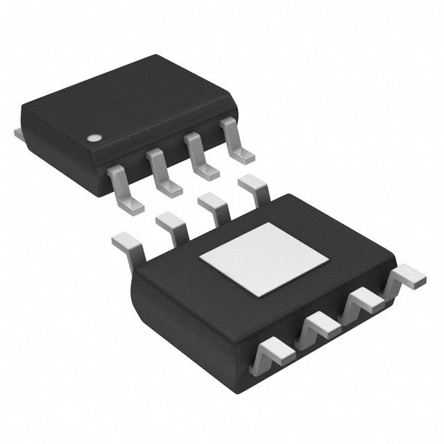
| 描述 | IC OPAMP JFET 1MHZ 8SOIC运算放大器 - 运放 Low-Power JFET-Input Op Amp |
| 产品分类 | Linear - Amplifiers - Instrumentation, OP Amps, Buffer Amps集成电路 - IC |
| 品牌 | Texas Instruments |
| 产品手册 | |
| 产品图片 |
|
| rohs | 符合RoHS无铅 / 符合限制有害物质指令(RoHS)规范要求 |
| 产品系列 | 放大器 IC,运算放大器 - 运放,Texas Instruments TL062BCDR- |
| 数据手册 | |
| 产品型号 | TL062BCDR |
| 产品种类 | 运算放大器 - 运放 |
| 供应商器件封装 | 8-SOIC |
| 共模抑制比—最小值 | 80 dB |
| 关闭 | No Shutdown |
| 其它名称 | 296-14988-1 |
| 包装 | 剪切带 (CT) |
| 单位重量 | 72.600 mg |
| 单电源电压 | 7 V to 36 V |
| 压摆率 | 3.5 V/µs |
| 双重电源电压 | +/- 5 V, +/- 9 V, +/- 12 V, +/- 15 V |
| 商标 | Texas Instruments |
| 增益带宽生成 | 1 MHz |
| 增益带宽积 | 1MHz |
| 安装类型 | 表面贴装 |
| 安装风格 | SMD/SMT |
| 封装 | Reel |
| 封装/外壳 | 8-SOIC(0.154",3.90mm 宽) |
| 封装/箱体 | SOIC-8 |
| 工作温度 | 0°C ~ 70°C |
| 工作电源电压 | 7 V to 36 V, +/- 3.5 V to +/- 18 V |
| 工厂包装数量 | 2500 |
| 技术 | BiFET |
| 放大器类型 | J-FET |
| 最大双重电源电压 | +/- 18 V |
| 最大工作温度 | + 70 C |
| 最小双重电源电压 | +/- 3.5 V |
| 最小工作温度 | 0 C |
| 标准包装 | 1 |
| 电压-电源,单/双 (±) | 7 V ~ 36 V, ±3.5 V ~ 18 V |
| 电压-输入失调 | 2mV |
| 电流-电源 | 200µA |
| 电流-输入偏置 | 30pA |
| 电流-输出/通道 | - |
| 电源电流 | 0.5 mA |
| 电路数 | 2 |
| 系列 | TL062B |
| 转换速度 | 3.5 V/us |
| 输入偏压电流—最大 | 200 pA |
| 输入参考电压噪声 | 42 nV |
| 输入补偿电压 | 3 mV |
| 输出类型 | - |
| 通道数量 | 2 Channel |


- 商务部:美国ITC正式对集成电路等产品启动337调查
- 曝三星4nm工艺存在良率问题 高通将骁龙8 Gen1或转产台积电
- 太阳诱电将投资9.5亿元在常州建新厂生产MLCC 预计2023年完工
- 英特尔发布欧洲新工厂建设计划 深化IDM 2.0 战略
- 台积电先进制程称霸业界 有大客户加持明年业绩稳了
- 达到5530亿美元!SIA预计今年全球半导体销售额将创下新高
- 英特尔拟将自动驾驶子公司Mobileye上市 估值或超500亿美元
- 三星加码芯片和SET,合并消费电子和移动部门,撤换高东真等 CEO
- 三星电子宣布重大人事变动 还合并消费电子和移动部门
- 海关总署:前11个月进口集成电路产品价值2.52万亿元 增长14.8%


PDF Datasheet 数据手册内容提取
Product Sample & Technical Tools & Support & Folder Buy Documents Software Community TL061,TL061A,TL061B TL062,TL062A,TL062B,TL064,TL064A,TL064B SLOS078L–NOVEMBER1978–REVISEDMAY2015 TL06xx Low-Power JFET-Input Operational Amplifiers 1 Features 2 Applications • VeryLowPowerConsumption • Tablets 1 • TypicalSupplyCurrent:200μA(PerAmplifier) • Whitegoods • WideCommon-ModeandDifferentialVoltage • Personalelectronics Ranges • Computers • LowInputBiasandOffsetCurrents 3 Description • Common-ModeInputVoltageRange IncludesV The JFET-input operational amplifiers of the TL06x CC+ series are designed as low-power versions of the • OutputShort-CircuitProtection TL08x series amplifiers. They feature high input • HighInputImpedance:JFET-InputStage impedance, wide bandwidth, high slew rate, and low • InternalFrequencyCompensation input offset and input bias currents. The TL06x series • Latch-Up-FreeOperation featuresthesameterminalassignmentsastheTL07x andTL08xseries. • HighSlewRate:3.5V/μsTypical • OnProductsComplianttoMIL-PRF-38535, DeviceInformation(1) AllParametersAreTestedUnlessOtherwise PARTNUMBER PACKAGE BODYSIZE(NOM) Noted.OnAllOtherProducts,Production TL06xxD SOIC(14) 8.65mm×3.91mm ProcessingDoesNotNecessarilyIncludeTesting TL06xxJ CDIP(14) 19.56mm×6.92mm ofAllParameters. TL06xxN PDIP(14) 19.30mm×6.35mm TL06xxNS SO(14) 10.30mm×5.30mm TL06xxPW TSSOP(14) 5.00mm×4.40mm (1) For all available packages, see the orderable addendum at theendofthedatasheet. SchematicSymbol IN+ + OUT IN− − OFFSETN1 OFFSET N2 Offset Null/Compensation TL061 Only 1 An IMPORTANT NOTICE at the end of this data sheet addresses availability, warranty, changes, use in safety-critical applications, intellectualpropertymattersandotherimportantdisclaimers.PRODUCTIONDATA.
TL061,TL061A,TL061B TL062,TL062A,TL062B,TL064,TL064A,TL064B SLOS078L–NOVEMBER1978–REVISEDMAY2015 www.ti.com Table of Contents 1 Features.................................................................. 1 8.2 FunctionalBlockDiagram.......................................14 2 Applications........................................................... 1 8.3 FeatureDescription.................................................14 3 Description............................................................. 1 8.4 DeviceFunctionalModes........................................15 4 RevisionHistory..................................................... 2 9 ApplicationsandImplementation...................... 16 9.1 ApplicationInformation............................................16 5 PinConfigurationandFunctions......................... 3 9.2 TypicalApplications................................................16 6 Specifications......................................................... 4 9.3 SystemExamples...................................................17 6.1 AbsoluteMaximumRatings......................................4 10 PowerSupplyRecommendations..................... 19 6.2 ESDRatings..............................................................5 11 Layout................................................................... 20 6.3 RecommendedOperatingConditions.......................5 6.4 ThermalInformation-8Pins.....................................5 11.1 LayoutGuidelines.................................................20 6.5 ThermalInformation-14Pins...................................5 11.2 LayoutExamples...................................................20 6.6 ThermalInformation-20Pins...................................6 12 DeviceandDocumentationSupport................. 21 6.7 ElectricalCharacteristicsforTL06xCandTL06xxC.6 12.1 DocumentationSupport........................................21 6.8 ElectricalCharacteristicsforTL06xxCandTL06xI...7 12.2 RelatedLinks........................................................21 6.9 ElectricalCharacteristicsforTL06xMandTL064M..7 12.3 CommunityResources..........................................21 6.10 OperatingCharacteristics........................................8 12.4 Trademarks...........................................................21 6.11 TypicalCharacteristics............................................9 12.5 ElectrostaticDischargeCaution............................21 7 ParameterMeasurementInformation................13 12.6 Glossary................................................................21 8 DetailedDescription............................................ 14 13 Mechanical,Packaging,andOrderable Information........................................................... 21 8.1 Overview.................................................................14 4 Revision History NOTE:Pagenumbersforpreviousrevisionsmaydifferfrompagenumbersinthecurrentversion. ChangesfromRevisionK(January2014)toRevisionL Page • AddedApplications................................................................................................................................................................. 1 • AddedPinConfigurationandFunctionssection,ESDRatingstable,FeatureDescriptionsection,DeviceFunctional Modes,ApplicationandImplementationsection,PowerSupplyRecommendationssection,Layoutsection,Device andDocumentationSupportsection,andMechanical,Packaging,andOrderableInformationsection .............................. 1 ChangesfromRevisionJ(September2004)toRevisionK Page • UpdateddocumenttonewTIdatasheetformat-nospecificationchanges......................................................................... 1 • DeletedOrderingInformationtable........................................................................................................................................ 1 • UpdatedFeatureswithMilitaryDisclaimer............................................................................................................................. 1 2 SubmitDocumentationFeedback Copyright©1978–2015,TexasInstrumentsIncorporated ProductFolderLinks:TL061 TL061A TL061BTL062 TL062A TL062B TL064 TL064A TL064B
TL061,TL061A,TL061B TL062,TL062A,TL062B,TL064,TL064A,TL064B www.ti.com SLOS078L–NOVEMBER1978–REVISEDMAY2015 5 Pin Configuration and Functions TL061xD,P,andPSPackage 8-PinSOIC,PDIP,andSO TL062FKPackage TopView 20-PinLCCC TopView OFFSETN1 1 8 NC T + U C IN− 2 7 VCC+ NC 1O NC VCNC IN+ 3 6 OUT VCC− 4 5 OFFSETN2 NC 43 2 1 20 1918 NC 1IN− 5 17 2OUT NC 6 16 NC TL062xD,JG,P,PS,andPWPackage 1IN+ 7 15 2IN− 8-PinSOIC,CDIP,PDIP,SO,andTSSOP NC 8 14 NC TopView 9 10 11 12 13 1OUT 1 8 VCC+ C − C+ C 1IN− 2 7 2OUT N CC N2IN N V 1IN+ 3 6 2IN− VCC− 4 5 2IN+ TL064FKPackage 20-PinLCCC TopView TL064xD,J,N,NS,PW,andWPackage T T 14-PinSOIC,CDIP,PDIP,SO,TSSOPandCFP − U U − TopView 1IN 1O NC4O 4IN 1OUT 1 14 4OUT 3 2 1 20 19 1IN+ 4 18 4IN+ 1IN− 2 13 4IN− NC 5 17 NC 1IN+ 3 12 4IN+ VCC+ 6 16 VCC− VCC+ 4 11 VCC− NC 7 15 NC 2IN+ 5 10 3IN+ 2IN+ 8 14 3IN+ 2IN− 6 9 3IN− 9 10 11 12 13 2OUT 7 8 3OUT − T CT − N U NU N 2I O O 3I 2 3 PinFunctions PIN TL061 TL062 TL064 TYPE DESCRIPTION NAME D,JG,P, D,J,N,NS, D,P,PS FK FK PS,PW PW,W 1IN– — 2 5 2 3 I Negativeinput 1IN+ — 3 7 3 4 I Positiveinput 1OUT — 1 2 1 2 O Output 2IN– — 6 15 6 9 I Negativeinput 2IN+ — 5 12 5 8 I Positiveinput 2OUT — 7 17 7 10 O Output 3IN– — — — 9 13 I Negativeinput 3IN+ — — — 10 14 I Positiveinput 3OUT — — — 8 12 O Output 4IN– — — — 13 19 I Negativeinput 4IN+ — — — 12 18 I Positiveinput 4OUT — — — 14 20 O Output IN– 2 — — — — I Negativeinput Copyright©1978–2015,TexasInstrumentsIncorporated SubmitDocumentationFeedback 3 ProductFolderLinks:TL061 TL061A TL061BTL062 TL062A TL062B TL064 TL064A TL064B
TL061,TL061A,TL061B TL062,TL062A,TL062B,TL064,TL064A,TL064B SLOS078L–NOVEMBER1978–REVISEDMAY2015 www.ti.com PinFunctions(continued) PIN TL061 TL062 TL064 TYPE DESCRIPTION NAME D,JG,P, D,J,N,NS, D,P,PS FK FK PS,PW PW,W IN+ 3 — — — — I Positiveinput 1 1 3 4 5 6 8 7 9 NC 8 — — — Donotconnect 11 11 13 14 15 16 18 17 19 OFFSETN1 1 — — — — — Inputoffsetadjustment OFFSETN2 5 — — — — — Inputoffsetadjustment OUT 6 — — — — O Output V 4 4 10 11 16 — Powersupply CC– V 7 8 20 4 6 — Powersupply CC+ 6 Specifications 6.1 Absolute Maximum Ratings overoperatingfree-airtemperaturerange(unlessotherwisenoted)(1) MIN MAX UNIT V 18 CC+ Supplyvoltage(2) V V –18 CC– V Differentialinputvoltage(3) ±30 V ID V Inputvoltage(2)(4) ±15 V I Durationofoutputshortcircuit(5) Unlimited T Operatingvirtualjunctiontemperature 150 °C J Casetemperaturefor60seconds FKpackage 260 °C Leadtemperature1.6mm(1/16inch)from J,JG,U,orWpackage 300 °C casefor60seconds Leadtemperature1.6mm(1/16inch)from D,N,NS,P,PS,orPWpackage 260 °C casefor10seconds T Storagetemperature –65 150 °C stg (1) StressesbeyondthoselistedunderAbsoluteMaximumRatingsmaycausepermanentdamagetothedevice.Thesearestressratings only,andfunctionaloperationofthedeviceattheseoranyotherconditionsbeyondthoseindicatedunderRecommendedOperating Conditionsisnotimplied.Exposuretoabsolute-maximum-ratedconditionsforextendedperiodsmayaffectdevicereliability. (2) Allvoltagevalues,exceptdifferentialvoltages,arewithrespecttothemidpointbetweenV andV . CC+ CC− (3) DifferentialvoltagesareatIN+,withrespecttoIN−. (4) Themagnitudeoftheinputvoltagemustneverexceedthemagnitudeofthesupplyvoltageor15V,whicheverisless. (5) Theoutputmaybeshortedtogroundortoeithersupply.Temperatureand/orsupplyvoltagesmustbelimitedtoensurethatthe dissipationratingisnotexceeded. 4 SubmitDocumentationFeedback Copyright©1978–2015,TexasInstrumentsIncorporated ProductFolderLinks:TL061 TL061A TL061BTL062 TL062A TL062B TL064 TL064A TL064B
TL061,TL061A,TL061B TL062,TL062A,TL062B,TL064,TL064A,TL064B www.ti.com SLOS078L–NOVEMBER1978–REVISEDMAY2015 6.2 ESD Ratings VALUE UNIT Humanbodymodel(HBM),perANSI/ESDA/JEDECJS-001(1) 2000 V(ESD) Electrostaticdischarge Charged-devicemodel(CDM),perJEDECspecificationJESD22- V C101(2) 2000 (1) JEDECdocumentJEP155statesthat500-VHBMallowssafemanufacturingwithastandardESDcontrolprocess. (2) JEDECdocumentJEP157statesthat250-VCDMallowssafemanufacturingwithastandardESDcontrolprocess. 6.3 Recommended Operating Conditions overoperatingfree-airtemperaturerange(unlessotherwisenoted) MIN MAX UNIT V Supplyvoltage 5 15 V CC+ V Supplyvoltage –5 –15 V CC– V Common-modevoltage V +4 V –4 V CM CC– CC+ TL06xM –55 125 TL06xQ –40 125 T Ambienttemperature °C A TL06xI –40 85 TL06xC 0 70 6.4 Thermal Information - 8 Pins TL06xx THERMALMETRIC(1) D(SOIC) P(PDIP) PS(SO) PW(TSSOP) JG(CDIP) UNIT 8PINS 8PINS 8PINS 8PINS 8PINS R Junction-to-ambientthermal θJ resistance(2)(3) 97 85 95 149 — °C/W A R θJ Junction-to-case(top)thermal C(to resistance(4)(5) — — — — 14.5 °C/W p) (1) Formoreinformationabouttraditionalandnewthermalmetrics,seetheSemiconductorandICPackageThermalMetricsapplication report,SPRA953. (2) MaximumpowerdissipationisafunctionofT ,R ,andT .Themaximumallowablepowerdissipationatanyallowableambient J(max) θJA A temperatureisP =(T –T )/R .OperatingattheabsolutemaximumT of150°Ccanaffectreliability. D J(max) A θJA J (3) ThepackagethermalimpedanceiscalculatedinaccordancewithJESD51-7. (4) MaximumpowerdissipationisafunctionofT ,R ,andT .Themaximumallowablepowerdissipationatanyallowableambient J(max) θJC C temperatureisP =(T –T )/R .OperatingattheabsolutemaximumT of150°Ccanaffectreliability. D J(max) C θJC J (5) ThepackagethermalimpedanceiscalculatedinaccordancewithMIL-STD-883. 6.5 Thermal Information - 14 Pins TL06xx THERMALMETRIC(1) D(SOIC) N(PDIP) NS(SO) PS(SO) PW J(CDIP) W(CFP) UNIT (TSSOP) 14PINS 14PINS 14PINS 8PINS 14PINS 14PINS 14PINS R Junction-to-ambientthermal 113 θJ resistance(2)(3) 86 80 76 95 — — °C/W A R θJ Junction-to-case(top)thermal C(to resistance(2)(3) — — — — — 15.05 14.65 °C/W p) (1) Formoreinformationabouttraditionalandnewthermalmetrics,seetheSemiconductorandICPackageThermalMetricsapplication report,SPRA953. (2) MaximumpowerdissipationisafunctionofT ,R ,andT .Themaximumallowablepowerdissipationatanyallowableambient J(max) θJC C temperatureisP =(T –T )/R .OperatingattheabsolutemaximumT of150°Ccanaffectreliability. D J(max) C θJC J (3) ThepackagethermalimpedanceiscalculatedinaccordancewithMIL-STD-883. Copyright©1978–2015,TexasInstrumentsIncorporated SubmitDocumentationFeedback 5 ProductFolderLinks:TL061 TL061A TL061BTL062 TL062A TL062B TL064 TL064A TL064B
TL061,TL061A,TL061B TL062,TL062A,TL062B,TL064,TL064A,TL064B SLOS078L–NOVEMBER1978–REVISEDMAY2015 www.ti.com 6.6 Thermal Information - 20 Pins TL06xx THERMALMETRIC(1) FK(LCCC) UNIT 20PINS R Junction-to-ambientthermalresistance(2)(3) — °C/W θJA R Junction-to-case(top)thermalresistance(4)(5) 5.61 °C/W θJC(top) (1) Formoreinformationabouttraditionalandnewthermalmetrics,seetheSemiconductorandICPackageThermalMetricsapplication report,SPRA953. (2) MaximumpowerdissipationisafunctionofT ,R ,andT .Themaximumallowablepowerdissipationatanyallowableambient J(max) θJA A temperatureisP =(T –T )/R .OperatingattheabsolutemaximumT of150°Ccanaffectreliability. D J(max) A θJA J (3) ThepackagethermalimpedanceiscalculatedinaccordancewithJESD51-7. (4) MaximumpowerdissipationisafunctionofT ,R ,andT .Themaximumallowablepowerdissipationatanyallowableambient J(max) θJC C temperatureisP =(T –T )/R .OperatingattheabsolutemaximumT of150°Ccanaffectreliability. D J(max) C θJC J (5) ThepackagethermalimpedanceiscalculatedinaccordancewithMIL-STD-883. 6.7 Electrical Characteristics for TL06xC and TL06xxC V =±15V(unlessotherwisenoted) CC± TL061AC,TL062AC, TL061C,TL062C,TL064C PARAMETER TESTCONDITIONS(1) TL064AC UNIT MIN TYP MAX MIN TYP MAX TA=25°C 3 15 3 6 VIO Inputoffsetvoltage VO=0,RS=50Ω mV TA=Fullrange 20 7.5 Temperaturecoefficient αVIO ofinputoffsetvoltage VO=0,RS=50Ω,TA=Fullrange 10 10 μV/°C TA=25°C 5 200 5 100 pA IIO Inputoffsetcurrent VO=0 TA=Fullrange 5 3 nA IIB Inputbiascurrent(2) VO=0 TA=25°C 30 400 30 200 pA TA=Fullrange 10 7 nA –12 –12 Common-modeinput VICR voltagerange TA=25°C ±11 to ±11 to V 15 15 Maximumpeakoutput RL=10kΩ,TA=25°C ±10 ±13.5 ±10 ±13.5 VOM voltageswing RL≥10kΩ,TA=Fullrange ±10 ±10 V AVD Lvoalrtgaeg-esiagmnapllidfiicffaetrioenntial VROL≥=2±1k0ΩV, TTAA==2F5u°llCrange 33 6 44 6 V/mV B1 Unity-gainbandwidth RL=10kΩ,TA=25°C 1 1 MHz ri Inputresistance TA=25°C 1012 1012 Ω CMRR Common-mode VIC=VICRmin, 70 86 80 86 dB rejectionratio VO=0,RS=50Ω,TA=25°C Supply-voltage kSVR r(ΔejVeCctCio±/nΔVraIOti)o VVCOC==0±,9RSV=to5±01Ω5,VT,A=25°C 70 95 80 95 dB Totalpowerdissipation PD (eachamplifier) VO=0,Noload,TA=25°C 6 7.5 6 7.5 mW Supplycurrent ICC (eachamplifier) VO=0,Noload,TA=25°C 200 250 200 250 µA VO1/VO2 Crosstalkattenuation AVD=100,TA=25°C 120 120 dB (1) Allcharacteristicsaremeasuredunderopen-loopconditionswithzerocommon-modeinputvoltageunlessotherwisespecified.Full rangeforT is0°Cto70°CforTL06xC,TL06xAC,andTL06xBCand–40°Cto85°CforTL06xI. A (2) InputbiascurrentsofanFET-inputoperationalamplifierarenormaljunctionreversecurrents,whicharetemperaturesensitive,as showninFigure12.Pulsetechniquesareusedtomaintainthejunctiontemperatureasclosetotheambienttemperatureaspossible. 6 SubmitDocumentationFeedback Copyright©1978–2015,TexasInstrumentsIncorporated ProductFolderLinks:TL061 TL061A TL061BTL062 TL062A TL062B TL064 TL064A TL064B
TL061,TL061A,TL061B TL062,TL062A,TL062B,TL064,TL064A,TL064B www.ti.com SLOS078L–NOVEMBER1978–REVISEDMAY2015 6.8 Electrical Characteristics for TL06xxC and TL06xI V =±15V(unlessotherwisenoted) CC± TL061BC,TL062BC, TL061I,TL062I,TL064I PARAMETER TESTCONDITIONS(1) TL064BC UNIT MIN TYP MAX MIN TYP MAX TA=25°C 2 3 3 6 VIO Inputoffsetvoltage VO=0,RS=50Ω mV TA=Fullrange 5 9 Temperaturecoefficient αVIO ofinputoffsetvoltage VO=0,RS=50Ω,TA=Fullrange 10 10 μV/°C TA=25°C 5 100 5 100 pA IIO Inputoffsetcurrent VO=0 TA=Fullrange 3 10 nA IIB Inputbiascurrent(2) VO=0 TA=25°C 30 200 30 200 pA TA=Fullrange 7 20 nA –12 –12 Common-modeinput VICR voltagerange TA=25°C ±11 to ±11 to V 15 15 Maximumpeakoutput RL=10kΩ,TA=25°C ±10 ±13.5 ±10 ±13.5 VOM voltageswing RL≥10kΩ,TA=Fullrange ±10 ±10 V AVD Lvoalrtgaeg-esiagmnapllidfiicffaetrioenntial VROL≥=2±1k0ΩV, TTAA==2F5u°llCrange 44 6 44 6 V/mV B1 Unity-gainbandwidth RL=10kΩ,TA=25°C 1 1 MHz ri Inputresistance TA=25°C 1012 1012 Ω CMRR Common-mode VIC=VICRmin, 80 86 80 86 dB rejectionratio VO=0,RS=50Ω,TA=25°C Supply-voltage kSVR r(ΔejVeCctCio±/nΔVraIOti)o VVCOC==0±,9RSV=to5±01Ω5,VT,A=25°C 80 95 80 95 dB Totalpowerdissipation PD (eachamplifier) VO=0,Noload,TA=25°C 6 7.5 6 7.5 mW Supplycurrent ICC (eachamplifier) VO=0,Noload,TA=25°C 200 250 200 250 µA VO1/VO2 Crosstalkattenuation AVD=100,TA=25°C 120 120 dB (1) Allcharacteristicsaremeasuredunderopen-loopconditionswithzerocommon-modeinputvoltage,unlessotherwisespecified.Full rangeforT is0°Cto70°CforTL06xC,TL06xAC,andTL06xBCand–40°Cto85°CforTL06xI. A (2) InputbiascurrentsofanFET-inputoperationalamplifierarenormaljunctionreversecurrents,whicharetemperaturesensitive,as showninFigure12.Pulsetechniquesareusedtomaintainthejunctiontemperatureasclosetotheambienttemperatureaspossible. 6.9 Electrical Characteristics for TL06xM and TL064M V =±15V(unlessotherwisenoted) CC± TL061M,TL062M TL064M PARAMETER TESTCONDITIONS(1) UNIT MIN TYP MAX MIN TYP MAX TA=25°C 3 6 3 9 VIO Inputoffsetvoltage VO=0,RS=50Ω TA=–55°Cto 9 15 mV 125°C αVIO Tofeimnppuetraotfufsreetcvooeltfaficgieent VTAO==–05,5R°SC=to5012Ω5,°C 10 10 μV/°C TA=25°C 5 100 5 100 pA IIO Inputoffsetcurrent VO=0 TA=–55°C 20(2) 20(2) nA TA=125°C 20 20 TA=25°C 30 200 30 200 pA IIB Inputbiascurrent(3) VO=0 TA=–55°C 50(2) 50(2) nA TA=125°C 50 50 –12 –12 Common-modeinput VICR voltagerange TA=25°C ±11 to ±11 to V 15 15 (1) Allcharacteristicsaremeasuredunderopen-loopconditions,withzerocommon-modevoltage,unlessotherwisespecified. (2) Thisparameterisnotproductiontested. (3) InputbiascurrentsofanFET-inputoperationalamplifierarenormaljunctionreversecurrents,whicharetemperaturesensitive,as showninFigure12.Pulsetechniquesareusedtomaintainthejunctiontemperatureasclosetotheambienttemperatureaspossible. Copyright©1978–2015,TexasInstrumentsIncorporated SubmitDocumentationFeedback 7 ProductFolderLinks:TL061 TL061A TL061BTL062 TL062A TL062B TL064 TL064A TL064B
TL061,TL061A,TL061B TL062,TL062A,TL062B,TL064,TL064A,TL064B SLOS078L–NOVEMBER1978–REVISEDMAY2015 www.ti.com Electrical Characteristics for TL06xM and TL064M (continued) V =±15V(unlessotherwisenoted) CC± TL061M,TL062M TL064M PARAMETER TESTCONDITIONS(1) UNIT MIN TYP MAX MIN TYP MAX Maximumpeakoutput RL=10kΩ,TA=25°C ±10 ±13.5 ±10 ±13.5 VOM voltageswing RL≥10kΩ,TA=–55°Cto125°C ±10 ±10 V TA=25°C 4 6 4 6 AVD Lvoalrtgaeg-esiagmnapllidfiicffaetrioenntial VROL≥=2±1k0ΩV, TA=–55°Cto 4 4 V/mV 125°C B1 Unity-gainbandwidth RL=10kΩ,TA=25°C MHz ri Inputresistance TA=25°C 1012 1012 Ω CMRR Common-mode VIC=VICRmin, 80 86 80 86 dB rejectionratio VO=0,RS=50Ω,TA=25°C Supply-voltage kSVR r(ΔejVeCctCio±/nΔVraIOti)o VVCOC==0±,9RSV=to5±01Ω5,VT,A=25°C 80 95 80 95 dB Totalpowerdissipation PD (eachamplifier) VO=0,Noload,TA=25°C 6 7.5 6 7.5 mW Supplycurrent ICC (eachamplifier) VO=0,Noload,TA=25°C 200 250 200 250 µA VO1/VO2 Crosstalkattenuation AVD=100,TA=25°C 120 120 dB 6.10 Operating Characteristics V =±15V,T =25°C CC± A PARAMETER TESTCONDITIONS MIN TYP MAX UNIT SR Slewrateatunitygain(1) VI=10V, CL=100pF, 1.5 3.5 V/μs R =10kΩ, seeFigure16 L tr Rise-time VI=20V, CL=100pF, 0.2 μs Overshootfactor RL=10kΩ, seeFigure16 10% V Equivalentinputnoisevoltage R =20Ω f=1kHz 42 nV/√Hz n S (1) Slewrateat–55°Cto125°Cis0.7V/μsmin. 8 SubmitDocumentationFeedback Copyright©1978–2015,TexasInstrumentsIncorporated ProductFolderLinks:TL061 TL061A TL061BTL062 TL062A TL062B TL064 TL064A TL064B
TL061,TL061A,TL061B TL062,TL062A,TL062B,TL064,TL064A,TL064B www.ti.com SLOS078L–NOVEMBER1978–REVISEDMAY2015 6.11 Typical Characteristics Dataathighandlowtemperaturesareapplicableonlywithinthespecifiedoperatingfree-airtemperaturerangesofthe variousdevices. Table1.TableofGraphs FIGURE MaximumpeakoutputvoltageversusSupplyvoltage Figure1 MaximumpeakoutputvoltageversusFree-airtemperature Figure2 MaximumpeakoutputvoltageversusLoadresistance Figure3 MaximumpeakoutputvoltageversusFrequency Figure4 DifferentialvoltageamplificationversusFree-airtemperature Figure5 Large-signaldifferentialvoltageamplificationversusFrequency Figure6 PhaseshiftversusFrequency Figure6 SupplycurrentversusSupplyvoltage Figure7 SupplycurrentversusFree-airtemperature Figure8 TotalpowerdissipationversusFree-airtemperature Figure9 Common-moderejectionratioversusFree-airtemperature Figure10 Normalizedunity-gainbandwidthversusFree-airtemperature Figure11 NormalizedslewrateversusFree-airtemperature Figure11 NormalizedphaseshiftversusFree-airtemperature Figure11 InputbiascurrentversusFree-airtemperature Figure12 Voltage-followerlarge-signalpulseresponseversusTime Figure13 OutputvoltageversusElapsedtime Figure14 EquivalentinputnoisevoltageversusFrequency Figure15 Copyright©1978–2015,TexasInstrumentsIncorporated SubmitDocumentationFeedback 9 ProductFolderLinks:TL061 TL061A TL061BTL062 TL062A TL062B TL064 TL064A TL064B
TL061,TL061A,TL061B TL062,TL062A,TL062B,TL064,TL064A,TL064B SLOS078L–NOVEMBER1978–REVISEDMAY2015 www.ti.com ±15 ±15 −V RL= 10 kΩ −V ge ±12.5 TA= 25°C ge±12.5 olta See Figure 2 olta V V ut ±10 ut ±10 p p ut ut O O k k ea ±7.5 ea ±7.5 P P m m u u xim ±5 xim ±5 a a M M − − VOM ±2.5 VOM ±2.5 VCC±=±15 V RL= 10 kΩ See Figure 2 0 0 0 2 4 6 8 10 12 14 16 −75 −50 −25 0 25 50 75 100 125 |VCC±|−Supply Voltage−V TA−Free-AirTemperature−°C Figure1.MaximumPeakOutputVoltagevsSupplyVoltage Figure2.MaximumPeakOutputVoltagevsFree-Air Temperature ±15 −V TVACC=± 2=5°±C15 V −V VCC±=±15 V RTAL== 2150° kCΩ Voltage ±12.5 SeeFigure2 Voltage ±12.5 VCC±=±12 V See Figure 2 Output ±10 Output ±10 Peak ±7.5 Peak ±7.5 m m Maximu ±5 Maximu ±5 VCC±=±5 V − − M ±2.5 M ±2.5 VO VO 0 0 100 200 400 700 1k 2k 4k 7k10k 1 k 10k 100k 1M 10 M RL−Load Resistance−Ω f−Frequency−Hz Figure3.MaximumPeakOutputVoltagevsLoad Figure4.MaximumPeakOutputVoltagevsFrequency Resistance 10 100 V/mV 7 VRCLC=± 1=0 ±k1Ω5 V VRCexCt±== 0±15 V n− 10 RL= 10 kΩ 0° DifferentialVoltageAmplificatio 24 −Large-Signal DifferentialAVDVoltageAmplification−V/mV 0.00.111 (lefAtVscDale) (TPrAihgah=st e2 s 5Sc°ahClieft) 491503°°5°Phase Shift − D V A 1 0.001 180° −75 −50 −25 0 25 50 75 100 125 1 10 100 1k 10k 100k 1M 10M TA−Free-AirTemperature−°C f−Frequency−Hz Figure5.DifferentialVoltageAmplificationvsFree-Air Figure6.Large-SignalDifferentialVoltageAmplificationand Temperature PhaseShiftvsFrequency 10 SubmitDocumentationFeedback Copyright©1978–2015,TexasInstrumentsIncorporated ProductFolderLinks:TL061 TL061A TL061BTL062 TL062A TL062B TL064 TL064A TL064B
TL061,TL061A,TL061B TL062,TL062A,TL062B,TL064,TL064A,TL064B www.ti.com SLOS078L–NOVEMBER1978–REVISEDMAY2015 250 250 TA= 25°C No Signal No Load 200 200 µA− µA− Supply Current 110500 Supply Current 110500 IICC−±CC IICC−±CC 50 50 VCC±=±15 V No Signal No Load 0 0 0 2 4 6 8 10 12 14 16 −75 |VCC±|−Supply Voltage−V TA−Free-AirTemperature−°C Figure7.SupplyCurrentvsSupplyVoltage Figure8.SupplyCurrentvsFree-AirTemperature 30 87 B VCC±=±15 V d RL= 10 kΩ − W 25 o 86 ssipation−m 20 VNNCoo CLS±oiga=nda±l15 V TL064 Rejection Rati 85 Di 15 de 84 wer Mo Po TL062 on- −Total 10 TL061 Comm 83 DD − PP 5 R 82 R M C 0 81 −75 −50 −25 0 25 50 75 100 125 −75 −50 −25 0 25 50 75 100 125 TA−Free-AirTemperature−°C TA−Free-AirTemperature−°C Figure9.TotalPowerDissipationvsFree-AirTemperature Figure10.AllExceptTL06_CCommon-ModeRejection RatiovsFree-AirTemperature 1.3 1.03 100 ate 40 VCC±=±15 V R w Unity-Gain Bandwidth e 1.2 1.02 nd Sl (left scale) P(rhigahste s Schalieft) nA 10 a − dth 1.1 1.01 hift ent 4 d Unity-Gain Bandwi 0.19 S(leleftw s Rcaaltee) 10.99 Normalized Phase S IIB−Input Bias CurrIIB 00..141 malize 0.8 RVLCC= ±1=0 k±Ω15 V 0.98 0.04 or f = B1 for Phase Shift N 0.7 0.97 0.01 −75 −50 −25 0 25 50 75 100 125 −50 −25 0 25 50 75 100 125 TA−Free-AirTemperature−°C TA−Free-AirTemperature−°C Figure11.NormalizedUnity-GainBandwidth,SlewRate, Figure12.InputBiasCurrentvsFree-AirTemperature andPhaseShiftvsFree-AirTemperature Copyright©1978–2015,TexasInstrumentsIncorporated SubmitDocumentationFeedback 11 ProductFolderLinks:TL061 TL061A TL061BTL062 TL062A TL062B TL064 TL064A TL064B
TL061,TL061A,TL061B TL062,TL062A,TL062B,TL064,TL064A,TL064B SLOS078L–NOVEMBER1978–REVISEDMAY2015 www.ti.com 6 28 Input 24 4 Overshoot −V mV 20 s Voltage 2 oltage− 16 Output 0 Output utputV 12 d O 8 an −2 − nput VCC±=±15 V VO 4 I −4 RL= 10 kΩ 10% VCC±=±15 V CL= 100 pF 0 RL= 10 kΩ TA= 25°C tr TA= 25°C −4 −6 0 2 4 6 8 10 0 0.2 0.4 0.6 0.8 1 1.2 1.4 t−Time−µs t−ElapsedTime−µs Figure13.Voltage-FollowerLarge-SignalPulseResponse Figure14.OutputVoltagevsElapsedTime vsTime 100 z VCC±=±15 V H 90 RS= 20Ω V/ TA= 25°C n 80 − ge 70 a olt V 60 e s oi 50 N ut p 40 n I ent 30 al v ui 20 q E − 10 n V 0 10 40 100 400 1k 4k 10k 40k 100k f−Frequency−Hz Figure15.EquivalentInputNoiseVoltagevsFrequency 12 SubmitDocumentationFeedback Copyright©1978–2015,TexasInstrumentsIncorporated ProductFolderLinks:TL061 TL061A TL061BTL062 TL062A TL062B TL064 TL064A TL064B
TL061,TL061A,TL061B TL062,TL062A,TL062B,TL064,TL064A,TL064B www.ti.com SLOS078L–NOVEMBER1978–REVISEDMAY2015 7 Parameter Measurement Information − OUT VI + CL= 100 pF RL= 2 kΩ Figure16.Unity-GainAmplifier 10kΩ 1 kΩ VI − OUT + RL CL= 100 pF Figure17.Gain-of-10InvertingAmplifier IN− − TL061 OUT IN+ N2 + N1 100kΩ 1.5 kΩ VCC− Figure18.InputOffset-VoltageNullCircuit Copyright©1978–2015,TexasInstrumentsIncorporated SubmitDocumentationFeedback 13 ProductFolderLinks:TL061 TL061A TL061BTL062 TL062A TL062B TL064 TL064A TL064B
TL061,TL061A,TL061B TL062,TL062A,TL062B,TL064,TL064A,TL064B SLOS078L–NOVEMBER1978–REVISEDMAY2015 www.ti.com 8 Detailed Description 8.1 Overview The JFET-input operational amplifiers of the TL06x series are designed as low-power versions of the TL08x series amplifiers. They feature high input impedance, wide bandwidth, high slew rate, and low input offset and input bias currents. The TL06x series features the same terminal assignments as the TL07x and TL08x series. Each of these JFET-input operational amplifiers incorporates well-matched, high-voltage JFET and bipolar transistorsinanintegratedcircuit. The C-suffix devices are characterized for operation from 0°C to 70°C. The I-suffix devices are characterized for operation from −40°C to 85°C, and the M-suffix devices are characterized for operation over the full military temperaturerangeof −55°Cto125°C. 8.2 Functional Block Diagram VCC+ IN+ 50Ω IN− 100Ω C1 OFFSET N1 OFFSET N2 OUT VCC− TL061 Only C1 = 10 pF onTL061,TL062, andTL064 Component values shown are nominal. 8.3 Feature Description 8.3.1 Common-ModeRejectionRatio The common-mode rejection ratio (CMRR) of an amplifier is a measure of how well the device rejects unwanted input signals common to both input leads. It is found by taking the ratio of the change in input offset voltage to the change in the input voltage and converting to decibels. Ideally the CMRR is infinite, but in practice, amplifiers aredesignedtohaveitashighaspossible.TheCMRRofthisdeviceis86dB. 8.3.2 SlewRate The slew rate is the rate at which an operational amplifier can change its output when there is a change on the input.Thesedeviceshavea3.5-V/μsslewrate. 14 SubmitDocumentationFeedback Copyright©1978–2015,TexasInstrumentsIncorporated ProductFolderLinks:TL061 TL061A TL061BTL062 TL062A TL062B TL064 TL064A TL064B
TL061,TL061A,TL061B TL062,TL062A,TL062B,TL064,TL064A,TL064B www.ti.com SLOS078L–NOVEMBER1978–REVISEDMAY2015 8.4 Device Functional Modes These devices are powered on when the supply is connected. This device can be operated as a single supply operationalamplifierordualsupplyamplifierdependingontheapplication. Copyright©1978–2015,TexasInstrumentsIncorporated SubmitDocumentationFeedback 15 ProductFolderLinks:TL061 TL061A TL061BTL062 TL062A TL062B TL064 TL064A TL064B
TL061,TL061A,TL061B TL062,TL062A,TL062B,TL064,TL064A,TL064B SLOS078L–NOVEMBER1978–REVISEDMAY2015 www.ti.com 9 Applications and Implementation NOTE Information in the following applications sections is not part of the TI component specification, and TI does not warrant its accuracy or completeness. TI’s customers are responsible for determining suitability of components for their purposes. Customers should validateandtesttheirdesignimplementationtoconfirmsystemfunctionality. 9.1 Application Information The TL06x series of operational amplifiers can be used in countless applications. The few applications in this sectionshowprinciplesusedinallapplicationsoftheseparts. 9.2 Typical Applications 9.2.1 InvertingAmplifierApplication A typical application for an operational amplifier in an inverting amplifier. This amplifier takes a positive voltage on the input, and makes it a negative voltage of the same magnitude. In the same manner, it also makes negativevoltagespositive. RF Vsup+ RI V OUT + V IN Vsup- Figure19. SchematicforInvertingAmplifierApplication 9.2.1.1 DesignRequirements The supply voltage must be chosen such that it is larger than the input voltage range and output range. For instance, this application will scale a signal of ±0.5 V to ±1.8 V. Setting the supply at ±12 V is sufficient to accommodatethisapplication. 9.2.1.2 DetailedDesignProcedure Determinethegainrequiredbytheinvertingamplifier: (1) (2) Once the desired gain is determined, choose a value for RI or RF. Choosing a value in the kilohm range is desirable because the amplifier circuit will use currents in the milliamp range. This ensures the part will not draw too much current. This example will choose 10 kΩ for RI which means 36 kΩ will be used for RF. This was determinedbyEquation3. (3) 16 SubmitDocumentationFeedback Copyright©1978–2015,TexasInstrumentsIncorporated ProductFolderLinks:TL061 TL061A TL061BTL062 TL062A TL062B TL064 TL064A TL064B
TL061,TL061A,TL061B TL062,TL062A,TL062B,TL064,TL064A,TL064B www.ti.com SLOS078L–NOVEMBER1978–REVISEDMAY2015 Typical Applications (continued) 9.2.1.3 ApplicationCurve 2 VIN 1.5 VOUT 1 0.5 olts 0 V -0.5 -1 -1.5 -2 0 0.5 1 1.5 2 Time (ms) Figure20. InputandOutputVoltagesoftheInvertingAmplifier 9.3 System Examples 9.3.1 GeneralApplications VCC+ RF= 100 kΩ − 10 kΩ 10 kΩ 100 kΩ TL064 0.1% 0.1% 15 V InputA + VCC+ 3.3 kΩ Output − VCC− − TL061 TL064 Output + 100 kΩ CF= 3.3µF + 1 kΩ VCC+ VCC− VCC+ 1 MΩ −15V Input B + − 100 kΩ TL064 10 kΩ 10 kΩ TL064 100 kΩ 3.3 kΩ − 0.1% 0.1% + 9.1 kΩ 1 VCC− VCC− f=2π´R ´C F F Figure21.InstrumentationAmplifier Figure22.0.5-HzSquare-WaveOscillator VCC+ VCC+ − 1 MΩ TL064 OutputA − VCC+ + R1 TL061 − Input C3 R2 +VCC− Output Input 1µF +TL064 T−L064VCC+ Output B 100 kΩ + 100 kΩ R1=R2=2´R3=1.5MΩ VCC+ VCC+ R3 100µF 100 kΩ − C1 C2 C1=C2=C3=110pF TL064 OutputC 2 + 1 f = =1kHz O 2π´R1´C1 Figure23.High-QNotchFilter Figure24.Audio-DistributionAmplifier Copyright©1978–2015,TexasInstrumentsIncorporated SubmitDocumentationFeedback 17 ProductFolderLinks:TL061 TL061A TL061BTL062 TL062A TL062B TL064 TL064A TL064B
TL061,TL061A,TL061B TL062,TL062A,TL062B,TL064,TL064A,TL064B SLOS078L–NOVEMBER1978–REVISEDMAY2015 www.ti.com System Examples (continued) 15 V VCC+ 10kΩ 10 kΩ 0.1µF 10 kΩ 10 kΩ + 10 kΩ 1 MΩ TIL601 100 pF TL061 Output − 10 kΩ − 50Ω TL061 Output 10 kΩ + 10 kΩ N2 5 kΩ N1 0.1µF 10 kΩ 250 kΩ −15 V Figure25.Low-LevelLightDetectorPreamplifier Figure26.ACAmplifier 10 kΩ 100 kΩ 1 kΩ IN+ + 0.1µF 0.06µF 0.06µF + 1µF TL062 Output 47 kΩ T−L10.261MΩ 100 kΩ 0.00120 µkFΩ 50 kΩ − 100 kΩ 2.7 kΩ 100 kΩ 270Ω 0.003µF 0.001µF 100 kΩ 10 kΩ + 20µF 50 kΩ 0.02µF 1 kΩ 1 kΩ 100kΩ − TL062 IN− + Figure27.MicrophonePreamplifierWithTone Figure28.InstrumentationAmplifier Control 18 SubmitDocumentationFeedback Copyright©1978–2015,TexasInstrumentsIncorporated ProductFolderLinks:TL061 TL061A TL061BTL062 TL062A TL062B TL064 TL064A TL064B
TL061,TL061A,TL061B TL062,TL062A,TL062B,TL064,TL064A,TL064B www.ti.com SLOS078L–NOVEMBER1978–REVISEDMAY2015 System Examples (continued) ICPREAMPLIFIERRESPONSECHARACTERISTICS 25 Max Bass 20 Max Treble VCC±=±15 V 15 TA= 25°C B d 10 − n atio 5 c plifi 0 m A −5 e g olta −10 V −15 −20 Min MinBass Treble −25 20 40 100 200 400 1 k 2 k 4 k 10k 20 k f−Frequency−Hz 220kΩ 0.00375µF 0.003µF 10 kΩ 0.03µF 0.01µF 27 kΩ MIN MIN 100 kΩ 100 kΩ VCC+ Bass Treble VCC+ 10 kΩ 3.3 kΩ MAX MAX + + 100Ω 1µF TL062 0.03µF TL062 Output Input − − VCC− 0.003µF VCC− 100Ω 10 kΩ Balance 10 pF 10 pF 75µF+ 47 kΩ 5 kΩ + 50 pF Gain 68 kΩ 47µF Figure29.ICPreamplifier 10 Power Supply Recommendations CAUTION Supply voltages larger than 36 V for a single supply, or outside the range of ±18 V for a dual supply can permanently damage the device (see the Absolute Maximum Ratings). Place 0.1-μF bypass capacitors close to the power-supply pins to reduce errors coupling in from noisy or high impedancepowersupplies.Formoredetailedinformationonbypasscapacitorplacement,refertotheLayout. Copyright©1978–2015,TexasInstrumentsIncorporated SubmitDocumentationFeedback 19 ProductFolderLinks:TL061 TL061A TL061BTL062 TL062A TL062B TL064 TL064A TL064B
TL061,TL061A,TL061B TL062,TL062A,TL062B,TL064,TL064A,TL064B SLOS078L–NOVEMBER1978–REVISEDMAY2015 www.ti.com 11 Layout 11.1 Layout Guidelines Forbestoperationalperformanceofthedevice,usegoodPCBlayoutpractices,including: • Noise can propagate into analog circuitry through the power pins of the circuit as a whole, as well as the operational amplifier. Bypass capacitors are used to reduce the coupled noise by providing low impedance powersourceslocaltotheanalogcircuitry. – Connect low-ESR, 0.1-μF ceramic bypass capacitors between each supply pin and ground, placed as close to the device as possible. A single bypass capacitor from V+ to ground is applicable for single supplyapplications. • Separate grounding for analog and digital portions of circuitry is one of the simplest and most-effective methods of noise suppression. One or more layers on multilayer PCBs are usually devoted to ground planes. A ground plane helps distribute heat and reduces EMI noise pickup. Make sure to physically separate digital and analog grounds, paying attention to the flow of the ground current. For more detailed information, refer to CircuitBoardLayoutTechniques,(SLOA089). • To reduce parasitic coupling, run the input traces as far away from the supply or output traces as possible. If it is not possible to keep them separate, it is much better to cross the sensitive trace perpendicular as opposedtoinparallelwiththenoisytrace. • Place the external components as close to the device as possible. Keeping RF and RG close to the inverting inputminimizesparasiticcapacitance,asshowninLayoutExamples. • Keep the length of input traces as short as possible. Always remember that the input traces are the most sensitivepartofthecircuit. • Consider a driven, low-impedance guard ring around the critical traces. A guard ring can significantly reduce leakagecurrentsfromnearbytracesthatareatdifferentpotentials. 11.2 Layout Examples RIN VIN + VOUT RG RF Figure30. OperationalAmplifierSchematicforNoninvertingConfiguration Place components close to device and to each other to reduce parasitic errors Run the input traces as far away from the supply lines RF as possible NC NC VS+ Use low-ESR, ceramic RG bypass capacitor GND IN1í VCC+ VIN IN1+ OUT RIN VCCí NC GND Only needed for dual-supply operation GND VS- (or GND for single supply) VOUT Ground (GND) plane on another layer Figure31. OperationalAmplifierBoardLayoutforNoninvertingConfiguration 20 SubmitDocumentationFeedback Copyright©1978–2015,TexasInstrumentsIncorporated ProductFolderLinks:TL061 TL061A TL061BTL062 TL062A TL062B TL064 TL064A TL064B
TL061,TL061A,TL061B TL062,TL062A,TL062B,TL064,TL064A,TL064B www.ti.com SLOS078L–NOVEMBER1978–REVISEDMAY2015 12 Device and Documentation Support 12.1 Documentation Support 12.1.1 RelatedDocumentation Forrelateddocumentation,seethefollowing: CircuitBoardLayoutTechniques,SLOA089 12.2 Related Links The table below lists quick access links. Categories include technical documents, support and community resources,toolsandsoftware,andquickaccesstosampleorbuy. Table2.RelatedLinks TECHNICAL TOOLS& SUPPORT& PARTS PRODUCTFOLDER SAMPLE&BUY DOCUMENTS SOFTWARE COMMUNITY TL061 Clickhere Clickhere Clickhere Clickhere Clickhere TL061A Clickhere Clickhere Clickhere Clickhere Clickhere TL061B Clickhere Clickhere Clickhere Clickhere Clickhere TL062 Clickhere Clickhere Clickhere Clickhere Clickhere TL062A Clickhere Clickhere Clickhere Clickhere Clickhere TL062B Clickhere Clickhere Clickhere Clickhere Clickhere TL064 Clickhere Clickhere Clickhere Clickhere Clickhere TL064A Clickhere Clickhere Clickhere Clickhere Clickhere TL064B Clickhere Clickhere Clickhere Clickhere Clickhere 12.3 Community Resources The following links connect to TI community resources. Linked contents are provided "AS IS" by the respective contributors. They do not constitute TI specifications and do not necessarily reflect TI's views; see TI's Terms of Use. TIE2E™OnlineCommunity TI'sEngineer-to-Engineer(E2E)Community.Createdtofostercollaboration amongengineers.Ate2e.ti.com,youcanaskquestions,shareknowledge,exploreideasandhelp solveproblemswithfellowengineers. DesignSupport TI'sDesignSupport QuicklyfindhelpfulE2Eforumsalongwithdesignsupporttoolsand contactinformationfortechnicalsupport. 12.4 Trademarks E2EisatrademarkofTexasInstruments. 12.5 Electrostatic Discharge Caution Thesedeviceshavelimitedbuilt-inESDprotection.Theleadsshouldbeshortedtogetherorthedeviceplacedinconductivefoam duringstorageorhandlingtopreventelectrostaticdamagetotheMOSgates. 12.6 Glossary SLYZ022—TIGlossary. Thisglossarylistsandexplainsterms,acronyms,anddefinitions. 13 Mechanical, Packaging, and Orderable Information The following pages include mechanical packaging and orderable information. This information is the most current data available for the designated devices. This data is subject to change without notice and revision of thisdocument.Forbrowserbasedversionsofthisdatasheet,refertothelefthandnavigation. Copyright©1978–2015,TexasInstrumentsIncorporated SubmitDocumentationFeedback 21 ProductFolderLinks:TL061 TL061A TL061BTL062 TL062A TL062B TL064 TL064A TL064B
PACKAGE OPTION ADDENDUM www.ti.com 6-Feb-2020 PACKAGING INFORMATION Orderable Device Status Package Type Package Pins Package Eco Plan Lead/Ball Finish MSL Peak Temp Op Temp (°C) Device Marking Samples (1) Drawing Qty (2) (6) (3) (4/5) 81023022A ACTIVE LCCC FK 20 1 TBD POST-PLATE N / A for Pkg Type -55 to 125 81023022A TL062MFKB 8102302PA ACTIVE CDIP JG 8 1 TBD Call TI N / A for Pkg Type -55 to 125 8102302PA TL062M 81023032A ACTIVE LCCC FK 20 1 TBD POST-PLATE N / A for Pkg Type -55 to 125 81023032A TL064MFKB 8102303CA ACTIVE CDIP J 14 1 TBD Call TI N / A for Pkg Type -55 to 125 8102303CA TL064MJB 8102303DA ACTIVE CFP W 14 1 TBD Call TI N / A for Pkg Type -55 to 125 8102303DA TL064MWB TL061ACD ACTIVE SOIC D 8 75 Green (RoHS NIPDAU Level-1-260C-UNLIM 0 to 70 061AC & no Sb/Br) TL061ACDE4 ACTIVE SOIC D 8 75 Green (RoHS NIPDAU Level-1-260C-UNLIM 0 to 70 061AC & no Sb/Br) TL061ACDR ACTIVE SOIC D 8 2500 Green (RoHS NIPDAU Level-1-260C-UNLIM 0 to 70 061AC & no Sb/Br) TL061ACP ACTIVE PDIP P 8 50 Green (RoHS NIPDAU N / A for Pkg Type 0 to 70 TL061ACP & no Sb/Br) TL061BCP ACTIVE PDIP P 8 50 Green (RoHS NIPDAU N / A for Pkg Type 0 to 70 TL061BCP & no Sb/Br) TL061BCPE4 ACTIVE PDIP P 8 50 Green (RoHS NIPDAU N / A for Pkg Type 0 to 70 TL061BCP & no Sb/Br) TL061CD ACTIVE SOIC D 8 75 Green (RoHS NIPDAU Level-1-260C-UNLIM 0 to 70 TL061C & no Sb/Br) TL061CDR ACTIVE SOIC D 8 2500 Green (RoHS NIPDAU Level-1-260C-UNLIM 0 to 70 TL061C & no Sb/Br) TL061CP ACTIVE PDIP P 8 50 Green (RoHS NIPDAU N / A for Pkg Type 0 to 70 TL061CP & no Sb/Br) TL061CPSR ACTIVE SO PS 8 2000 Green (RoHS NIPDAU Level-1-260C-UNLIM 0 to 70 T061 & no Sb/Br) TL061ID ACTIVE SOIC D 8 75 Green (RoHS NIPDAU Level-1-260C-UNLIM -40 to 85 TL061I & no Sb/Br) TL061IDR ACTIVE SOIC D 8 2500 Green (RoHS NIPDAU Level-1-260C-UNLIM -40 to 85 TL061I & no Sb/Br) Addendum-Page 1
PACKAGE OPTION ADDENDUM www.ti.com 6-Feb-2020 Orderable Device Status Package Type Package Pins Package Eco Plan Lead/Ball Finish MSL Peak Temp Op Temp (°C) Device Marking Samples (1) Drawing Qty (2) (6) (3) (4/5) TL061IDRG4 ACTIVE SOIC D 8 2500 Green (RoHS NIPDAU Level-1-260C-UNLIM -40 to 85 TL061I & no Sb/Br) TL061IP ACTIVE PDIP P 8 50 Green (RoHS NIPDAU N / A for Pkg Type -40 to 85 TL061IP & no Sb/Br) TL061IPE4 ACTIVE PDIP P 8 50 Green (RoHS NIPDAU N / A for Pkg Type -40 to 85 TL061IP & no Sb/Br) TL062ACD ACTIVE SOIC D 8 75 Green (RoHS NIPDAU Level-1-260C-UNLIM 0 to 70 062AC & no Sb/Br) TL062ACDE4 ACTIVE SOIC D 8 75 Green (RoHS NIPDAU Level-1-260C-UNLIM 0 to 70 062AC & no Sb/Br) TL062ACDR ACTIVE SOIC D 8 2500 Green (RoHS NIPDAU Level-1-260C-UNLIM 0 to 70 062AC & no Sb/Br) TL062ACDRE4 ACTIVE SOIC D 8 2500 Green (RoHS NIPDAU Level-1-260C-UNLIM 0 to 70 062AC & no Sb/Br) TL062ACDRG4 ACTIVE SOIC D 8 2500 Green (RoHS NIPDAU Level-1-260C-UNLIM 0 to 70 062AC & no Sb/Br) TL062ACP ACTIVE PDIP P 8 50 Green (RoHS NIPDAU N / A for Pkg Type 0 to 70 TL062ACP & no Sb/Br) TL062ACPSR ACTIVE SO PS 8 2000 Green (RoHS NIPDAU Level-1-260C-UNLIM 0 to 70 T062A & no Sb/Br) TL062ACPSRG4 ACTIVE SO PS 8 2000 Green (RoHS NIPDAU Level-1-260C-UNLIM 0 to 70 T062A & no Sb/Br) TL062BCD ACTIVE SOIC D 8 75 Green (RoHS NIPDAU Level-1-260C-UNLIM 0 to 70 062BC & no Sb/Br) TL062BCDG4 ACTIVE SOIC D 8 75 Green (RoHS NIPDAU Level-1-260C-UNLIM 0 to 70 062BC & no Sb/Br) TL062BCDR ACTIVE SOIC D 8 2500 Green (RoHS NIPDAU Level-1-260C-UNLIM 0 to 70 062BC & no Sb/Br) TL062BCP ACTIVE PDIP P 8 50 Green (RoHS NIPDAU N / A for Pkg Type 0 to 70 TL062BCP & no Sb/Br) TL062BCPE4 ACTIVE PDIP P 8 50 Green (RoHS NIPDAU N / A for Pkg Type 0 to 70 TL062BCP & no Sb/Br) TL062CD ACTIVE SOIC D 8 75 Green (RoHS NIPDAU Level-1-260C-UNLIM 0 to 70 TL062C & no Sb/Br) TL062CDE4 ACTIVE SOIC D 8 75 Green (RoHS NIPDAU Level-1-260C-UNLIM 0 to 70 TL062C & no Sb/Br) Addendum-Page 2
PACKAGE OPTION ADDENDUM www.ti.com 6-Feb-2020 Orderable Device Status Package Type Package Pins Package Eco Plan Lead/Ball Finish MSL Peak Temp Op Temp (°C) Device Marking Samples (1) Drawing Qty (2) (6) (3) (4/5) TL062CDR ACTIVE SOIC D 8 2500 Green (RoHS NIPDAU Level-1-260C-UNLIM 0 to 70 TL062C & no Sb/Br) TL062CDRE4 ACTIVE SOIC D 8 2500 Green (RoHS NIPDAU Level-1-260C-UNLIM 0 to 70 TL062C & no Sb/Br) TL062CDRG4 ACTIVE SOIC D 8 2500 Green (RoHS NIPDAU Level-1-260C-UNLIM 0 to 70 TL062C & no Sb/Br) TL062CP ACTIVE PDIP P 8 50 Green (RoHS NIPDAU N / A for Pkg Type 0 to 70 TL062CP & no Sb/Br) TL062CPE4 ACTIVE PDIP P 8 50 Green (RoHS NIPDAU N / A for Pkg Type 0 to 70 TL062CP & no Sb/Br) TL062CPSR ACTIVE SO PS 8 2000 Green (RoHS NIPDAU Level-1-260C-UNLIM 0 to 70 T062 & no Sb/Br) TL062CPW ACTIVE TSSOP PW 8 150 Green (RoHS NIPDAU Level-1-260C-UNLIM 0 to 70 T062 & no Sb/Br) TL062CPWG4 ACTIVE TSSOP PW 8 150 Green (RoHS NIPDAU Level-1-260C-UNLIM 0 to 70 T062 & no Sb/Br) TL062CPWR ACTIVE TSSOP PW 8 2000 Green (RoHS NIPDAU Level-1-260C-UNLIM 0 to 70 T062 & no Sb/Br) TL062CPWRG4 ACTIVE TSSOP PW 8 2000 Green (RoHS NIPDAU Level-1-260C-UNLIM 0 to 70 T062 & no Sb/Br) TL062ID ACTIVE SOIC D 8 75 Green (RoHS NIPDAU Level-1-260C-UNLIM -40 to 85 TL062I & no Sb/Br) TL062IDG4 ACTIVE SOIC D 8 75 Green (RoHS NIPDAU Level-1-260C-UNLIM -40 to 85 TL062I & no Sb/Br) TL062IDR ACTIVE SOIC D 8 2500 Green (RoHS NIPDAU Level-1-260C-UNLIM -40 to 85 TL062I & no Sb/Br) TL062IDRG4 ACTIVE SOIC D 8 2500 Green (RoHS NIPDAU Level-1-260C-UNLIM -40 to 85 TL062I & no Sb/Br) TL062IP ACTIVE PDIP P 8 50 Green (RoHS NIPDAU N / A for Pkg Type -40 to 85 TL062IP & no Sb/Br) TL062IPE4 ACTIVE PDIP P 8 50 Green (RoHS NIPDAU N / A for Pkg Type -40 to 85 TL062IP & no Sb/Br) TL062IPWR ACTIVE TSSOP PW 8 2000 Green (RoHS NIPDAU Level-1-260C-UNLIM -40 to 85 Z062 & no Sb/Br) TL062IPWRG4 ACTIVE TSSOP PW 8 2000 Green (RoHS NIPDAU Level-1-260C-UNLIM -40 to 85 Z062 & no Sb/Br) Addendum-Page 3
PACKAGE OPTION ADDENDUM www.ti.com 6-Feb-2020 Orderable Device Status Package Type Package Pins Package Eco Plan Lead/Ball Finish MSL Peak Temp Op Temp (°C) Device Marking Samples (1) Drawing Qty (2) (6) (3) (4/5) TL062MFKB ACTIVE LCCC FK 20 1 TBD POST-PLATE N / A for Pkg Type -55 to 125 81023022A TL062MFKB TL062MJG ACTIVE CDIP JG 8 1 TBD Call TI N / A for Pkg Type -55 to 125 TL062MJG TL062MJGB ACTIVE CDIP JG 8 1 TBD Call TI N / A for Pkg Type -55 to 125 8102302PA TL062M TL064ACD ACTIVE SOIC D 14 50 Green (RoHS NIPDAU Level-1-260C-UNLIM 0 to 70 TL064AC & no Sb/Br) TL064ACDR ACTIVE SOIC D 14 2500 Green (RoHS NIPDAU Level-1-260C-UNLIM 0 to 70 TL064AC & no Sb/Br) TL064ACDRE4 ACTIVE SOIC D 14 2500 Green (RoHS NIPDAU Level-1-260C-UNLIM 0 to 70 TL064AC & no Sb/Br) TL064ACN ACTIVE PDIP N 14 25 Green (RoHS NIPDAU N / A for Pkg Type 0 to 70 TL064ACN & no Sb/Br) TL064BCD ACTIVE SOIC D 14 50 Green (RoHS NIPDAU Level-1-260C-UNLIM 0 to 70 TL064BC & no Sb/Br) TL064BCDG4 ACTIVE SOIC D 14 50 Green (RoHS NIPDAU Level-1-260C-UNLIM 0 to 70 TL064BC & no Sb/Br) TL064BCDR ACTIVE SOIC D 14 2500 Green (RoHS NIPDAU Level-1-260C-UNLIM 0 to 70 TL064BC & no Sb/Br) TL064BCN ACTIVE PDIP N 14 25 Green (RoHS NIPDAU N / A for Pkg Type 0 to 70 TL064BCN & no Sb/Br) TL064BCNE4 ACTIVE PDIP N 14 25 Green (RoHS NIPDAU N / A for Pkg Type 0 to 70 TL064BCN & no Sb/Br) TL064CD ACTIVE SOIC D 14 50 Green (RoHS NIPDAU Level-1-260C-UNLIM 0 to 70 TL064C & no Sb/Br) TL064CDE4 ACTIVE SOIC D 14 50 Green (RoHS NIPDAU Level-1-260C-UNLIM 0 to 70 TL064C & no Sb/Br) TL064CDR ACTIVE SOIC D 14 2500 Green (RoHS NIPDAU Level-1-260C-UNLIM 0 to 70 TL064C & no Sb/Br) TL064CDRE4 ACTIVE SOIC D 14 2500 Green (RoHS NIPDAU Level-1-260C-UNLIM 0 to 70 TL064C & no Sb/Br) TL064CN ACTIVE PDIP N 14 25 Green (RoHS NIPDAU N / A for Pkg Type 0 to 70 TL064CN & no Sb/Br) TL064CNSR ACTIVE SO NS 14 2000 Green (RoHS NIPDAU Level-1-260C-UNLIM 0 to 70 TL064 & no Sb/Br) Addendum-Page 4
PACKAGE OPTION ADDENDUM www.ti.com 6-Feb-2020 Orderable Device Status Package Type Package Pins Package Eco Plan Lead/Ball Finish MSL Peak Temp Op Temp (°C) Device Marking Samples (1) Drawing Qty (2) (6) (3) (4/5) TL064CPW ACTIVE TSSOP PW 14 90 Green (RoHS NIPDAU Level-1-260C-UNLIM 0 to 70 T064 & no Sb/Br) TL064CPWE4 ACTIVE TSSOP PW 14 90 Green (RoHS NIPDAU Level-1-260C-UNLIM 0 to 70 T064 & no Sb/Br) TL064CPWG4 ACTIVE TSSOP PW 14 90 Green (RoHS NIPDAU Level-1-260C-UNLIM 0 to 70 T064 & no Sb/Br) TL064CPWR ACTIVE TSSOP PW 14 2000 Green (RoHS NIPDAU Level-1-260C-UNLIM 0 to 70 T064 & no Sb/Br) TL064ID ACTIVE SOIC D 14 50 Green (RoHS NIPDAU Level-1-260C-UNLIM -40 to 85 TL064I & no Sb/Br) TL064IDG4 ACTIVE SOIC D 14 50 Green (RoHS NIPDAU Level-1-260C-UNLIM -40 to 85 TL064I & no Sb/Br) TL064IDR ACTIVE SOIC D 14 2500 Green (RoHS NIPDAU | SN Level-1-260C-UNLIM -40 to 85 TL064I & no Sb/Br) TL064IDRG4 ACTIVE SOIC D 14 2500 Green (RoHS NIPDAU Level-1-260C-UNLIM -40 to 85 TL064I & no Sb/Br) TL064IN ACTIVE PDIP N 14 25 Green (RoHS NIPDAU N / A for Pkg Type -40 to 85 TL064IN & no Sb/Br) TL064INE4 ACTIVE PDIP N 14 25 Green (RoHS NIPDAU N / A for Pkg Type -40 to 85 TL064IN & no Sb/Br) TL064INS ACTIVE SO NS 14 50 Green (RoHS NIPDAU Level-1-260C-UNLIM -40 to 85 TL064I & no Sb/Br) TL064INSR ACTIVE SO NS 14 2000 Green (RoHS NIPDAU Level-1-260C-UNLIM -40 to 85 TL064I & no Sb/Br) TL064IPWR ACTIVE TSSOP PW 14 2000 Green (RoHS NIPDAU Level-1-260C-UNLIM -40 to 85 Z064 & no Sb/Br) TL064MFKB ACTIVE LCCC FK 20 1 TBD POST-PLATE N / A for Pkg Type -55 to 125 81023032A TL064MFKB TL064MJ ACTIVE CDIP J 14 1 TBD Call TI N / A for Pkg Type -55 to 125 TL064MJ TL064MJB ACTIVE CDIP J 14 1 TBD Call TI N / A for Pkg Type -55 to 125 8102303CA TL064MJB TL064MWB ACTIVE CFP W 14 1 TBD Call TI N / A for Pkg Type -55 to 125 8102303DA TL064MWB (1) The marketing status values are defined as follows: ACTIVE: Product device recommended for new designs. Addendum-Page 5
PACKAGE OPTION ADDENDUM www.ti.com 6-Feb-2020 LIFEBUY: TI has announced that the device will be discontinued, and a lifetime-buy period is in effect. NRND: Not recommended for new designs. Device is in production to support existing customers, but TI does not recommend using this part in a new design. PREVIEW: Device has been announced but is not in production. Samples may or may not be available. OBSOLETE: TI has discontinued the production of the device. (2) RoHS: TI defines "RoHS" to mean semiconductor products that are compliant with the current EU RoHS requirements for all 10 RoHS substances, including the requirement that RoHS substance do not exceed 0.1% by weight in homogeneous materials. Where designed to be soldered at high temperatures, "RoHS" products are suitable for use in specified lead-free processes. TI may reference these types of products as "Pb-Free". RoHS Exempt: TI defines "RoHS Exempt" to mean products that contain lead but are compliant with EU RoHS pursuant to a specific EU RoHS exemption. Green: TI defines "Green" to mean the content of Chlorine (Cl) and Bromine (Br) based flame retardants meet JS709B low halogen requirements of <=1000ppm threshold. Antimony trioxide based flame retardants must also meet the <=1000ppm threshold requirement. (3) MSL, Peak Temp. - The Moisture Sensitivity Level rating according to the JEDEC industry standard classifications, and peak solder temperature. (4) There may be additional marking, which relates to the logo, the lot trace code information, or the environmental category on the device. (5) Multiple Device Markings will be inside parentheses. Only one Device Marking contained in parentheses and separated by a "~" will appear on a device. If a line is indented then it is a continuation of the previous line and the two combined represent the entire Device Marking for that device. (6) Lead/Ball Finish - Orderable Devices may have multiple material finish options. Finish options are separated by a vertical ruled line. Lead/Ball Finish values may wrap to two lines if the finish value exceeds the maximum column width. Important Information and Disclaimer:The information provided on this page represents TI's knowledge and belief as of the date that it is provided. TI bases its knowledge and belief on information provided by third parties, and makes no representation or warranty as to the accuracy of such information. Efforts are underway to better integrate information from third parties. TI has taken and continues to take reasonable steps to provide representative and accurate information but may not have conducted destructive testing or chemical analysis on incoming materials and chemicals. TI and TI suppliers consider certain information to be proprietary, and thus CAS numbers and other limited information may not be available for release. In no event shall TI's liability arising out of such information exceed the total purchase price of the TI part(s) at issue in this document sold by TI to Customer on an annual basis. OTHER QUALIFIED VERSIONS OF TL062, TL062M, TL064, TL064M : •Catalog: TL062, TL064 •Military: TL062M, TL064M NOTE: Qualified Version Definitions: •Catalog - TI's standard catalog product Addendum-Page 6
PACKAGE OPTION ADDENDUM www.ti.com 6-Feb-2020 •Military - QML certified for Military and Defense Applications Addendum-Page 7
PACKAGE MATERIALS INFORMATION www.ti.com 28-Dec-2019 TAPE AND REEL INFORMATION *Alldimensionsarenominal Device Package Package Pins SPQ Reel Reel A0 B0 K0 P1 W Pin1 Type Drawing Diameter Width (mm) (mm) (mm) (mm) (mm) Quadrant (mm) W1(mm) TL061ACDR SOIC D 8 2500 330.0 12.4 6.4 5.2 2.1 8.0 12.0 Q1 TL061CDR SOIC D 8 2500 330.0 12.4 6.4 5.2 2.1 8.0 12.0 Q1 TL061CDR SOIC D 8 2500 330.0 12.4 6.4 5.2 2.1 8.0 12.0 Q1 TL061IDR SOIC D 8 2500 330.0 12.4 6.4 5.2 2.1 8.0 12.0 Q1 TL061IDR SOIC D 8 2500 330.0 12.4 6.4 5.2 2.1 8.0 12.0 Q1 TL062ACDR SOIC D 8 2500 330.0 12.4 6.4 5.2 2.1 8.0 12.0 Q1 TL062BCDR SOIC D 8 2500 330.0 12.4 6.4 5.2 2.1 8.0 12.0 Q1 TL062CDR SOIC D 8 2500 330.0 12.4 6.4 5.2 2.1 8.0 12.0 Q1 TL062CDR SOIC D 8 2500 330.0 12.4 6.4 5.2 2.1 8.0 12.0 Q1 TL062CPWR TSSOP PW 8 2000 330.0 12.4 7.0 3.6 1.6 8.0 12.0 Q1 TL062CPWRG4 TSSOP PW 8 2000 330.0 12.4 7.0 3.6 1.6 8.0 12.0 Q1 TL062IDR SOIC D 8 2500 330.0 12.4 6.4 5.2 2.1 8.0 12.0 Q1 TL062IDR SOIC D 8 2500 330.0 12.4 6.4 5.2 2.1 8.0 12.0 Q1 TL062IPWR TSSOP PW 8 2000 330.0 12.4 7.0 3.6 1.6 8.0 12.0 Q1 TL064ACDR SOIC D 14 2500 330.0 16.4 6.5 9.0 2.1 8.0 16.0 Q1 TL064BCDR SOIC D 14 2500 330.0 16.4 6.5 9.0 2.1 8.0 16.0 Q1 TL064CDR SOIC D 14 2500 330.0 16.4 6.5 9.0 2.1 8.0 16.0 Q1 TL064CPWR TSSOP PW 14 2000 330.0 12.4 6.9 5.6 1.6 8.0 12.0 Q1 PackMaterials-Page1
PACKAGE MATERIALS INFORMATION www.ti.com 28-Dec-2019 Device Package Package Pins SPQ Reel Reel A0 B0 K0 P1 W Pin1 Type Drawing Diameter Width (mm) (mm) (mm) (mm) (mm) Quadrant (mm) W1(mm) TL064IDR SOIC D 14 2500 330.0 16.4 6.5 9.0 2.1 8.0 16.0 Q1 TL064IDRG4 SOIC D 14 2500 330.0 16.4 6.5 9.0 2.1 8.0 16.0 Q1 TL064INSR SO NS 14 2000 330.0 16.4 8.2 10.5 2.5 12.0 16.0 Q1 TL064IPWR TSSOP PW 14 2000 330.0 12.4 6.9 5.6 1.6 8.0 12.0 Q1 *Alldimensionsarenominal Device PackageType PackageDrawing Pins SPQ Length(mm) Width(mm) Height(mm) TL061ACDR SOIC D 8 2500 340.5 338.1 20.6 TL061CDR SOIC D 8 2500 340.5 338.1 20.6 TL061CDR SOIC D 8 2500 367.0 367.0 35.0 TL061IDR SOIC D 8 2500 340.5 338.1 20.6 TL061IDR SOIC D 8 2500 367.0 367.0 35.0 TL062ACDR SOIC D 8 2500 340.5 338.1 20.6 TL062BCDR SOIC D 8 2500 340.5 338.1 20.6 TL062CDR SOIC D 8 2500 340.5 338.1 20.6 TL062CDR SOIC D 8 2500 367.0 367.0 35.0 TL062CPWR TSSOP PW 8 2000 367.0 367.0 35.0 TL062CPWRG4 TSSOP PW 8 2000 367.0 367.0 35.0 TL062IDR SOIC D 8 2500 367.0 367.0 35.0 TL062IDR SOIC D 8 2500 340.5 338.1 20.6 PackMaterials-Page2
PACKAGE MATERIALS INFORMATION www.ti.com 28-Dec-2019 Device PackageType PackageDrawing Pins SPQ Length(mm) Width(mm) Height(mm) TL062IPWR TSSOP PW 8 2000 367.0 367.0 35.0 TL064ACDR SOIC D 14 2500 367.0 367.0 38.0 TL064BCDR SOIC D 14 2500 367.0 367.0 38.0 TL064CDR SOIC D 14 2500 367.0 367.0 38.0 TL064CPWR TSSOP PW 14 2000 367.0 367.0 35.0 TL064IDR SOIC D 14 2500 367.0 367.0 38.0 TL064IDRG4 SOIC D 14 2500 367.0 367.0 38.0 TL064INSR SO NS 14 2000 367.0 367.0 38.0 TL064IPWR TSSOP PW 14 2000 367.0 367.0 35.0 PackMaterials-Page3
None
None
None
None
PACKAGE OUTLINE J0014A CDIP - 5.08 mm max height SCALE 0.900 CERAMIC DUAL IN LINE PACKAGE PIN 1 ID A 4X .005 MIN (OPTIONAL) [0.13] .015-.060 TYP [0.38-1.52] 1 14 12X .100 [2.54] 14X .014-.026 14X .045-.065 [0.36-0.66] [1.15-1.65] .010 [0.25] C A B .754-.785 [19.15-19.94] 7 8 B .245-.283 .2 MAX TYP .13 MIN TYP [6.22-7.19] [5.08] [3.3] SEATING PLANE C .308-.314 [7.83-7.97] AT GAGE PLANE .015 GAGE PLANE [0.38] 0 -15 14X .008-.014 TYP [0.2-0.36] 4214771/A 05/2017 NOTES: 1. All controlling linear dimensions are in inches. Dimensions in brackets are in millimeters. Any dimension in brackets or parenthesis are for reference only. Dimensioning and tolerancing per ASME Y14.5M. 2. This drawing is subject to change without notice. 3. This package is hermitically sealed with a ceramic lid using glass frit. 4. Index point is provided on cap for terminal identification only and on press ceramic glass frit seal only. 5. Falls within MIL-STD-1835 and GDIP1-T14. www.ti.com
EXAMPLE BOARD LAYOUT J0014A CDIP - 5.08 mm max height CERAMIC DUAL IN LINE PACKAGE (.300 ) TYP [7.62] SEE DETAIL B SEE DETAIL A 1 14 12X (.100 ) [2.54] SYMM 14X ( .039) [1] 7 8 SYMM LAND PATTERN EXAMPLE NON-SOLDER MASK DEFINED SCALE: 5X .002 MAX (.063) [0.05] [1.6] METAL ALL AROUND ( .063) SOLDER MASK [1.6] OPENING METAL .002 MAX SOLDER MASK (R.002 ) TYP [0.05] OPENING [0.05] ALL AROUND DETAIL A DETAIL B SCALE: 15X 13X, SCALE: 15X 4214771/A 05/2017 www.ti.com
None
None
None
PACKAGE OUTLINE D0008A SOIC - 1.75 mm max height SCALE 2.800 SMALL OUTLINE INTEGRATED CIRCUIT C SEATING PLANE .228-.244 TYP [5.80-6.19] .004 [0.1] C A PIN 1 ID AREA 6X .050 [1.27] 8 1 2X .189-.197 [4.81-5.00] .150 NOTE 3 [3.81] 4X (0 -15 ) 4 5 8X .012-.020 B .150-.157 [0.31-0.51] .069 MAX [3.81-3.98] .010 [0.25] C A B [1.75] NOTE 4 .005-.010 TYP [0.13-0.25] 4X (0 -15 ) SEE DETAIL A .010 [0.25] .004-.010 0 - 8 [0.11-0.25] .016-.050 [0.41-1.27] DETAIL A (.041) TYPICAL [1.04] 4214825/C 02/2019 NOTES: 1. Linear dimensions are in inches [millimeters]. Dimensions in parenthesis are for reference only. Controlling dimensions are in inches. Dimensioning and tolerancing per ASME Y14.5M. 2. This drawing is subject to change without notice. 3. This dimension does not include mold flash, protrusions, or gate burrs. Mold flash, protrusions, or gate burrs shall not exceed .006 [0.15] per side. 4. This dimension does not include interlead flash. 5. Reference JEDEC registration MS-012, variation AA. www.ti.com
EXAMPLE BOARD LAYOUT D0008A SOIC - 1.75 mm max height SMALL OUTLINE INTEGRATED CIRCUIT 8X (.061 ) [1.55] SYMM SEE DETAILS 1 8 8X (.024) [0.6] SYMM (R.002 ) TYP [0.05] 5 4 6X (.050 ) [1.27] (.213) [5.4] LAND PATTERN EXAMPLE EXPOSED METAL SHOWN SCALE:8X SOLDER MASK SOLDER MASK METAL OPENING OPENING METAL UNDER SOLDER MASK EXPOSED METAL EXPOSED METAL .0028 MAX .0028 MIN [0.07] [0.07] ALL AROUND ALL AROUND NON SOLDER MASK SOLDER MASK DEFINED DEFINED SOLDER MASK DETAILS 4214825/C 02/2019 NOTES: (continued) 6. Publication IPC-7351 may have alternate designs. 7. Solder mask tolerances between and around signal pads can vary based on board fabrication site. www.ti.com
EXAMPLE STENCIL DESIGN D0008A SOIC - 1.75 mm max height SMALL OUTLINE INTEGRATED CIRCUIT 8X (.061 ) [1.55] SYMM 1 8 8X (.024) [0.6] SYMM (R.002 ) TYP [0.05] 5 4 6X (.050 ) [1.27] (.213) [5.4] SOLDER PASTE EXAMPLE BASED ON .005 INCH [0.125 MM] THICK STENCIL SCALE:8X 4214825/C 02/2019 NOTES: (continued) 8. Laser cutting apertures with trapezoidal walls and rounded corners may offer better paste release. IPC-7525 may have alternate design recommendations. 9. Board assembly site may have different recommendations for stencil design. www.ti.com
None
None
MECHANICAL DATA MCER001A – JANUARY 1995 – REVISED JANUARY 1997 JG (R-GDIP-T8) CERAMIC DUAL-IN-LINE 0.400 (10,16) 0.355 (9,00) 8 5 0.280 (7,11) 0.245 (6,22) 1 4 0.065 (1,65) 0.045 (1,14) 0.063 (1,60) 0.020 (0,51) MIN 0.310 (7,87) 0.015 (0,38) 0.290 (7,37) 0.200 (5,08) MAX Seating Plane 0.130 (3,30) MIN 0.023 (0,58) 0°–15° 0.015 (0,38) 0.100 (2,54) 0.014 (0,36) 0.008 (0,20) 4040107/C 08/96 NOTES: A. All linear dimensions are in inches (millimeters). B. This drawing is subject to change without notice. C. This package can be hermetically sealed with a ceramic lid using glass frit. D. Index point is provided on cap for terminal identification. E. Falls within MIL STD 1835 GDIP1-T8 • POST OFFICE BOX 655303 DALLAS, TEXAS 75265
None
None
PACKAGE OUTLINE PW0008A TSSOP - 1.2 mm max height SCALE 2.800 SMALL OUTLINE PACKAGE C 6.6 TYP SEATING PLANE 6.2 PIN 1 ID A 0.1 C AREA 6X 0.65 8 1 3.1 2X 2.9 NOTE 3 1.95 4 5 0.30 8X 0.19 4.5 1.2 MAX B 0.1 C A B 4.3 NOTE 4 (0.15) TYP SEE DETAIL A 0.25 GAGE PLANE 0.15 0.75 0 - 8 0.05 0.50 DETAIL A TYPICAL 4221848/A 02/2015 NOTES: 1. All linear dimensions are in millimeters. Any dimensions in parenthesis are for reference only. Dimensioning and tolerancing per ASME Y14.5M. 2. This drawing is subject to change without notice. 3. This dimension does not include mold flash, protrusions, or gate burrs. Mold flash, protrusions, or gate burrs shall not exceed 0.15 mm per side. 4. This dimension does not include interlead flash. Interlead flash shall not exceed 0.25 mm per side. 5. Reference JEDEC registration MO-153, variation AA. www.ti.com
EXAMPLE BOARD LAYOUT PW0008A TSSOP - 1.2 mm max height SMALL OUTLINE PACKAGE 8X (1.5) 8X (0.45) SYMM (R0.05) 1 TYP 8 SYMM 6X (0.65) 5 4 (5.8) LAND PATTERN EXAMPLE SCALE:10X SOOPLEDNEINRG MASK METAL MSOELTDAEL RU NMDAESRK SOOPLEDNEINRG MASK 0.05 MAX 0.05 MIN ALL AROUND ALL AROUND NON SOLDER MASK SOLDER MASK DEFINED DEFINED SOLDER MASK DETAILS NOT TO SCALE 4221848/A 02/2015 NOTES: (continued) 6. Publication IPC-7351 may have alternate designs. 7. Solder mask tolerances between and around signal pads can vary based on board fabrication site. www.ti.com
EXAMPLE STENCIL DESIGN PW0008A TSSOP - 1.2 mm max height SMALL OUTLINE PACKAGE 8X (1.5) SYMM (R0.05) TYP 8X (0.45) 1 8 SYMM 6X (0.65) 5 4 (5.8) SOLDER PASTE EXAMPLE BASED ON 0.125 mm THICK STENCIL SCALE:10X 4221848/A 02/2015 NOTES: (continued) 8. Laser cutting apertures with trapezoidal walls and rounded corners may offer better paste release. IPC-7525 may have alternate design recommendations. 9. Board assembly site may have different recommendations for stencil design. www.ti.com
IMPORTANTNOTICEANDDISCLAIMER TI PROVIDES TECHNICAL AND RELIABILITY DATA (INCLUDING DATASHEETS), DESIGN RESOURCES (INCLUDING REFERENCE DESIGNS), APPLICATION OR OTHER DESIGN ADVICE, WEB TOOLS, SAFETY INFORMATION, AND OTHER RESOURCES “AS IS” AND WITH ALL FAULTS, AND DISCLAIMS ALL WARRANTIES, EXPRESS AND IMPLIED, INCLUDING WITHOUT LIMITATION ANY IMPLIED WARRANTIES OF MERCHANTABILITY, FITNESS FOR A PARTICULAR PURPOSE OR NON-INFRINGEMENT OF THIRD PARTY INTELLECTUAL PROPERTY RIGHTS. These resources are intended for skilled developers designing with TI products. You are solely responsible for (1) selecting the appropriate TI products for your application, (2) designing, validating and testing your application, and (3) ensuring your application meets applicable standards, and any other safety, security, or other requirements. These resources are subject to change without notice. TI grants you permission to use these resources only for development of an application that uses the TI products described in the resource. Other reproduction and display of these resources is prohibited. No license is granted to any other TI intellectual property right or to any third party intellectual property right. TI disclaims responsibility for, and you will fully indemnify TI and its representatives against, any claims, damages, costs, losses, and liabilities arising out of your use of these resources. TI’s products are provided subject to TI’s Terms of Sale (www.ti.com/legal/termsofsale.html) or other applicable terms available either on ti.com or provided in conjunction with such TI products. TI’s provision of these resources does not expand or otherwise alter TI’s applicable warranties or warranty disclaimers for TI products. Mailing Address: Texas Instruments, Post Office Box 655303, Dallas, Texas 75265 Copyright © 2020, Texas Instruments Incorporated