ICGOO在线商城 > 集成电路(IC) > 接口 - 编码器,解码器,转换器 > TIR1000IPSR
- 型号: TIR1000IPSR
- 制造商: Texas Instruments
- 库位|库存: xxxx|xxxx
- 要求:
| 数量阶梯 | 香港交货 | 国内含税 |
| +xxxx | $xxxx | ¥xxxx |
查看当月历史价格
查看今年历史价格
TIR1000IPSR产品简介:
ICGOO电子元器件商城为您提供TIR1000IPSR由Texas Instruments设计生产,在icgoo商城现货销售,并且可以通过原厂、代理商等渠道进行代购。 TIR1000IPSR价格参考。Texas InstrumentsTIR1000IPSR封装/规格:接口 - 编码器,解码器,转换器, Infrared Encoder/Decoder IC 8-SO。您可以下载TIR1000IPSR参考资料、Datasheet数据手册功能说明书,资料中有TIR1000IPSR 详细功能的应用电路图电压和使用方法及教程。
| 参数 | 数值 |
| 产品目录 | 集成电路 (IC) |
| 描述 | IC IRDA ENCODER/DECODER 8SO |
| 产品分类 | |
| 品牌 | Texas Instruments |
| 数据手册 | |
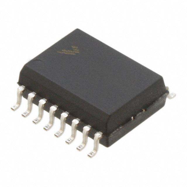
| 产品图片 |
|
| 产品型号 | TIR1000IPSR |
| rohs | 无铅 / 符合限制有害物质指令(RoHS)规范要求 |
| 产品系列 | - |
| 供应商器件封装 | 8-SO |
| 其它名称 | 296-27628-1 |
| 包装 | 剪切带 (CT) |
| 安装类型 | 表面贴装 |
| 封装/外壳 | 8-SOIC(0.209",5.30mm 宽) |
| 应用 | - |
| 标准包装 | 1 |
| 电压-电源,数字 | 2.7 V ~ 5.5 V |
| 电压-电源,模拟 | 2.7 V ~ 5.5 V |
| 类型 | 红外线编码器/解码器 |



PDF Datasheet 数据手册内容提取
Product Sample & Technical Tools & Support & Folder Buy Documents Software Community TIR1000,TIR1000I SLLS228G–DECEMBER1995–REVISEDAUGUST2015 TIR1000x Standalone IrDA™ Encoder and Decoder 1 Features 3 Description • AddsInfrared(IR)PorttoUniversalAsynchronous The TIR1000x serial infrared (SIR) encoder and 1 decoder is a CMOS device that encodes and ReceiverTransmitter(UART) decodes bit data in conformance with the IrDA • CompatibleWithInfraredDataAssociation specification. (IrDA™)andHewlettPackardSerialInfrared A transceiver device is needed to interface to the (HPSIR) photo-sensitive diode (PIN) and the light emitting • Provides1200-bpsto115-kbpsDataRate diode (LED). A UART is needed to interface to the • Operatesfrom2.7Vto5.5V serialdatalines. • ProvidesSimpleInterfaceWithUART DeviceInformation(1) • DecodesNegativeorPositivePulses PARTNUMBER PACKAGE BODYSIZE(NOM) • AvailableinTwo8-TerminalPlasticSmallOutline TSSOP(8) 3.00mm×4.40mm Packages(PSOP) TIR1000x SO(8) 6.20mm×5.30mm – PSPackageHasSlightlyLargerDimensions ThanPWPackage (1) For all available packages, see the orderable addendum at theendofthedatasheet. 2 Applications • UARTInterfacing • InfraredDataCommunications FunctionalBlockDiagram RESET IR_RXD Decoder U_RXD 16XCLK U_TXD Encoder IR_TXD 1 An IMPORTANT NOTICE at the end of this data sheet addresses availability, warranty, changes, use in safety-critical applications, intellectualpropertymattersandotherimportantdisclaimers.UNLESSOTHERWISENOTED,thisdocumentcontainsPRODUCTION DATA.
TIR1000,TIR1000I SLLS228G–DECEMBER1995–REVISEDAUGUST2015 www.ti.com Table of Contents 1 Features.................................................................. 1 7.3 FeatureDescription...................................................6 2 Applications........................................................... 1 7.4 DeviceFunctionalModes..........................................7 3 Description............................................................. 1 8 ApplicationandImplementation.......................... 9 4 RevisionHistory..................................................... 2 8.1 ApplicationInformation..............................................9 8.2 TypicalApplication ...................................................9 5 PinConfigurationandFunctions......................... 3 9 PowerSupplyRecommendations...................... 11 6 Specifications......................................................... 3 10 Layout................................................................... 12 6.1 AbsoluteMaximumRatings......................................3 6.2 ESDRatings ............................................................4 10.1 LayoutGuidelines.................................................12 6.3 RecommendedOperatingConditions.......................4 10.2 LayoutExample....................................................12 6.4 ThermalInformation..................................................4 11 DeviceandDocumentationSupport................. 13 6.5 ElectricalCharacteristics...........................................4 11.1 CommunityResources..........................................13 6.6 SwitchingCharacteristics..........................................5 11.2 Trademarks...........................................................13 7 DetailedDescription.............................................. 6 11.3 ElectrostaticDischargeCaution............................13 7.1 Overview...................................................................6 11.4 Glossary................................................................13 7.2 FunctionalBlockDiagram.........................................6 12 Mechanical,Packaging,andOrderable Information........................................................... 13 4 Revision History NOTE:Pagenumbersforpreviousrevisionsmaydifferfrompagenumbersinthecurrentversion. ChangesfromRevisionF(July1999)toRevisionG Page • AddedApplications,PinConfigurationandFunctionssection,ESDRatingstable,TypicalCharacteristicssection, FeatureDescriptionsection,DeviceFunctionalModes,ApplicationandImplementationsection,PowerSupply Recommendationssection,Layoutsection,DeviceandDocumentationSupportsection,andMechanical, Packaging,andOrderableInformationsection ..................................................................................................................... 1 • AddedPSpackagedrawing................................................................................................................................................... 3 • Changedt outputrisetimeFROM:1.3nsTO:23.8nsinSwitchingCharacteristics........................................................... 5 r • Changedt outputfalltimeFROM:1.8nsTO:9.2nsinSwitchingCharacteristics .............................................................. 5 f 2 SubmitDocumentationFeedback Copyright©1995–2015,TexasInstrumentsIncorporated ProductFolderLinks:TIR1000
TIR1000,TIR1000I www.ti.com SLLS228G–DECEMBER1995–REVISEDAUGUST2015 5 Pin Configuration and Functions PSPackage 8-PinSO PWPackage TopView 8-PinTSSOP TopView 16XCLK 1 8 VCC 1U6X_TCXLDK 12 87 IVRC_CTXD U_TXD 2 7 IR_TXD U_RXD 3 6 IR_RXD GND 4 5 RESET U_RXD 3 6 IR_RXD GND 4 5 RESET PinFunctions PIN I/O DESCRIPTION NAME NO. Clocksignal.16XCLKmustbesetto16timesthebaudrate.ThehighestbaudrateforIrDAis115.2kbps 16XCLK 1 I forwhichtheclockfrequencyequals1.843MHz(thisterminalistiedtotheBAUDOUTofaUART). GND 4 — Ground Infraredreceiverdata.IR_RXDisanIrDA-SIR-modulatedinputfromanoptoelectronicstransceiverwhose IR_RXD 6 I inputpulsesshouldbe3/16ofthebaudrateperiod. IR_TXD 7 O Infraredtransmitterdata.IR_TXDisanIrDA-SIR-modulatedoutputtoanoptoelectronicstransceiver. Activehighreset.RESETinitializesanIrDA-SIR-decode/encodestatemachine(thisterminalistiedtoa RESET 5 I UARTresetline). Receiverdata.U_RXDisdecoded(demodulated)datafromIR_RXDaccordingtotheIrDAspecification(this U_RXD 3 O terminalistiedtoSINofaUART). Transmitterdata.U_TXDisencoded(modulated)dataandoutputdataasIR_TXD(thisterminalistiedto U_TXD 2 I SOUTfromaUART). V 8 — Supplyvoltage CC 6 Specifications 6.1 Absolute Maximum Ratings overoperatingfree-airtemperaturerange(unlessotherwisenoted) (1) MIN MAX UNIT V Supplyvoltage(2) –0.5 6 V CC V Inputvoltageatanyinput –0.5 V +0.5 V I CC V Outputvoltage –0.5 V +0.5 V O CC TIR1000 0 °C T Operatingfree-airtemperaturerange A TIR1000I –40 85 °C Casetemperaturefor10seconds SOpackage 260 °C T Storagetemperature –65 150 °C stg (1) StressesbeyondthoselistedunderAbsoluteMaximumRatingsmaycausepermanentdamagetothedevice.Thesearestressratings only,whichdonotimplyfunctionaloperationofthedeviceattheseoranyotherconditionsbeyondthoseindicatedunderRecommended OperatingConditions.Exposuretoabsolute-maximum-ratedconditionsforextendedperiodsmayaffectdevicereliability. (2) AllvoltagelevelsarewithrespecttoGND. Copyright©1995–2015,TexasInstrumentsIncorporated SubmitDocumentationFeedback 3 ProductFolderLinks:TIR1000
TIR1000,TIR1000I SLLS228G–DECEMBER1995–REVISEDAUGUST2015 www.ti.com 6.2 ESD Ratings VALUE UNIT Human-bodymodel(HBM),perANSI/ESDA/JEDECJS-001(1) ±2000 V(ESD) Electrostaticdischarge Charged-devicemodel(CDM),perJEDECspecificationJESD22- V C101(2) ±900 (1) JEDECdocumentJEP155statesthat500-VHBMallowssafemanufacturingwithastandardESDcontrolprocess. (2) JEDECdocumentJEP157statesthat250-VCDMallowssafemanufacturingwithastandardESDcontrolprocess. 6.3 Recommended Operating Conditions overoperatingfree-airtemperaturerange(unlessotherwisenoted) MIN NOM MAX UNIT LOWVOLTAGE(3-VNOMINAL) V Supplyvoltage 2.7 3 3.3 V CC V High-levelinputvoltage 0.7V V IH CC V Low-levelinputvoltage 0.2V V IL CC Operatingfree-air TIR1000 0 70 T °C A temperature TIR1000I –40 85 STANDARDVOLTAGE(5-VNOMINAL) V Supplyvoltage 4.5 5 5.5 V CC V High-levelinputvoltage 0.7V V IH CC V Low-levelinputvoltage 0.2V V IL CC Operatingfree-air TIR1000 0 70 T °C A temperature TIR1000I –40 85 6.4 Thermal Information TIR1000 THERMALMETRIC(1) PS(SO),PW(TSSOP) UNIT 8PINS R Junction-to-ambientthermalresistance 179.8 °C/W θJA R Junction-to-case(top)thermalresistance 63.4 °C/W θJC(top) R Junction-to-boardthermalresistance 108.4 °C/W θJB ψ Junction-to-topcharacterizationparameter 7.0 °C/W JT ψ Junction-to-boardcharacterizationparameter 106.7 °C/W JB (1) Formoreinformationabouttraditionalandnewthermalmetrics,seetheSemiconductorandICPackageThermalMetricsapplication report,SPRA953. 6.5 Electrical Characteristics overoperatingfree-airtemperaturerange(unlessotherwisenoted) PARAMETER TESTCONDITIONS MIN TYP MAX UNIT I =–4mA V =5V V –0.8 OH CC CC V High-leveloutputvoltage V OH I =–1.8mA V =3V V –0.55 OH CC CC I =+4mA V =5V 0.5 OL CC V Low-leveloutputvoltage V OL I =+1.8mA V =3V 0.5 OL CC I IIInputcurrent V =0toV Allotherpinsfloating ±3 µA I I CC V =5.25V T =25°C CC A I Supplycurrent Allinputsat0.2V 16XCLKat2MHz 1 mA CC Noloadonoutputs C Clockinputcapacitance 5 pF i(16XCLK) f Clockfrequency 2 MHz (16XCLK) 4 SubmitDocumentationFeedback Copyright©1995–2015,TexasInstrumentsIncorporated ProductFolderLinks:TIR1000
TIR1000,TIR1000I www.ti.com SLLS228G–DECEMBER1995–REVISEDAUGUST2015 6.6 Switching Characteristics overoperatingfree-airtemperaturerange(unlessotherwisenoted) PARAMETER TESTCONDITIONS MIN TYP(1) MAX UNIT t Outputrisetime Noload 23.8 ns r t Outputfalltime Noload 9.2 ns f (1) TypicalvaluesareatT =25°C. A 16Cycles 16Cycles 16XCLK IR_RXD U_RXD ExternalStrobe 7Cycles 16 Cycles Figure1. RecommendedStrobingForDecodedData Copyright©1995–2015,TexasInstrumentsIncorporated SubmitDocumentationFeedback 5 ProductFolderLinks:TIR1000
TIR1000,TIR1000I SLLS228G–DECEMBER1995–REVISEDAUGUST2015 www.ti.com 7 Detailed Description 7.1 Overview TIR1000 serial infrared (SIR) encoder and decoder is a device (CMOS) that encodes and decodes bit data accordingwiththeIrDAspecifications. For the correct performance of the TIR1000 device, an optoelectronics device and a UART device are necessary.TheTIR1000deviceoperatesasaninterfacebetweenwirelessinfraredandUARTcommunication. 7.2 Functional Block Diagram RESET IR_RXD Decoder U_RXD 16XCLK U_TXD Encoder IR_TXD 7.3 Feature Description The Infrared Data Association (IrDA) defines several protocols for sending and receiving serial infrared data, includingthefollowingrates: • 115.2kbps • 0.576Mbps • 1.152Mbps • 4Mbps The low rate of 115.2 kbps was specified first and the others must maintain downward compatibility with it. At the 115.2 kbps rate, the protocol implemented in the hardware is fairly simple. It primarily defines a serial infrared data word to be surrounded by a start bit equal to 0 and a stop bit equal to 1. Individual bits are encoded or decodedthesamewhethertheyarestart,data,orstopbits. TheTIR1000andTIR1000Idevicesevaluateonlysinglebitsandfollowonlythe115.2-kbpsprotocol.The 115.2-kbps rate is a maximum rate. When both ends of the transfer are set up to a lower but matching speed, theprotocol(withtheTIR1000andTIR1000Idevices)stillworks. The clock used to code or sample the data is 16 times the baud rate, or 1.843 MHz maximum. To code a 1, no pulse is sent or received for 1-bit time period, or 16 clock cycles. To code a 0, one pulse is sent or received within a 1-bit time period, or 16 clock cycles. The pulse must be at least 1.6 μs wide and 3 clock cycles long at 1.843MHz.Atlowerbaudrates,thepulsecanbe1.6μswideoraslongas3clockcycles. The transmitter output, IR_TXD, is intended to drive an LED circuit to generate an infrared pulse. The LED circuits work on positive pulses. A terminal circuit is expected to create the receiver input, IR_RXD. Most (but not all) PIN circuits have inversion and generate negative pulses from the detected infrared light. Their output is normallyhigh.TheTIR1000andTIR1000IdevicescandecodeeithernegativeorpositivepulsesonIR_RXD. 6 SubmitDocumentationFeedback Copyright©1995–2015,TexasInstrumentsIncorporated ProductFolderLinks:TIR1000
TIR1000,TIR1000I www.ti.com SLLS228G–DECEMBER1995–REVISEDAUGUST2015 7.4 Device Functional Modes 7.4.1 IrDAEncoderFunction Serial data from a UART is encoded to transmit data to the optoelectronics. While the serial data input to this block (U_TXD) is high, the output (IR_TXD) is always low, and the counter used to form a pulse on IR_TXD is continuously cleared. After U_TXD resets to 0, IR_TXD rises on the falling edge of the seventh 16XCLK. On the falling edge of the tenth 16XCLK pulse, IR_TXD falls, creating a 3-clock-wide pulse. While U_TXD stays low, a pulseistransmittedduringtheseventhtotenthclocksofeach16-clockbitcycle. 16Cycles 16Cycles 16Cycles 16Cycles U_TXD 16XCLK 16XCLK U_TXD 1 2 3 4 5 6 7 8 10 12 14 16 IR_TXD IR_TXD Figure2. IrDA-SIREncodingScheme Figure3. EncodingScheme DetailedTimingDiagram MacroView 7.4.2 IrDADecoderFunction After reset, U_RXD is high and the 4-bit counter is cleared. When a falling edge is detected on IR_RXD, U_RXD falls on the next rising edge of 16XCLK with sufficient setup time. U_RXD stays low for 16 cycles (16XCLK) and then returns to high as required by the IrDA specification. As long as no pulses (falling edges) are detected on IR_RXD,U_RXDremainshigh. 16Cycles 16Cycles 16Cycles 16Cycles IR_RXD 16XCLK 16XCLK IR_RXD 1 2 3 4 5 6 7 8 10 12 14 16 U_RXD U_RXD Figure4. IrDA-SIRDecodingScheme Figure5. DecodingScheme DetailedTimingDiagram MacroView It is possible for jitter or slight frequency differences to cause the next falling edge on IR_RXD to be missed for one 16XCLK cycle. In that case, a 1-clock-wide pulse appears on U_RXD between consecutive zeroes. It is important for the UART to strobe U_RXD in the middle of the bit time to avoid latching this 1-clock-wide pulse. The TL16C550C UART already strobes incoming serial data at the proper time. Otherwise, note that data is required to be framed by a leading zero and a trailing one. The falling edge of that first zero on U_RXD synchronizes the read strobe. The strobe occurs on the eighth 16XCLK pulse after the U_RXD falling edge and onceevery16cyclesthereafteruntilthestopbitoccurs. Copyright©1995–2015,TexasInstrumentsIncorporated SubmitDocumentationFeedback 7 ProductFolderLinks:TIR1000
TIR1000,TIR1000I SLLS228G–DECEMBER1995–REVISEDAUGUST2015 www.ti.com IR_RXD 16XCLK 1 2 3 4 5 6 7 8 10 12 14 16 1 2 3 4 5 6 7 8 10 12 14 16 U_RXD Figure6. TimingCausing1-Clock-WidePulseBetweenConsecutiveOnes The TIR1000 and TIR1000I can decode positive pulses on IR_RXD. The timing is different, but the variation is invisible to the UART. The decoder, which works from the falling edge, now recognizes a zero on the trailing edge of the pulse rather than on the leading edge. As long as the pulse width is fairly constant, as defined by the specification, the trailing edges should also be 16 clock cycles apart and data can readily be decoded. The zero appearsonU_RXDafterthepulseratherthanatthestartofit. IR_RXD 16XCLK 1 2 3 4 5 6 7 8 10 12 14 16 U_RXD Figure7. PositiveIR_RXDPulseDecode DetailedView 16Cycles 16Cycles 16Cycles 16Cycles 16XCLK IR_RXD U_RXD Figure8. PositiveIR_RXDPulseDecode MacroView 8 SubmitDocumentationFeedback Copyright©1995–2015,TexasInstrumentsIncorporated ProductFolderLinks:TIR1000
TIR1000,TIR1000I www.ti.com SLLS228G–DECEMBER1995–REVISEDAUGUST2015 8 Application and Implementation NOTE Information in the following applications sections is not part of the TI component specification, and TI does not warrant its accuracy or completeness. TI’s customers are responsible for determining suitability of components for their purposes. Customers should validateandtesttheirdesignimplementationtoconfirmsystemfunctionality. 8.1 Application Information IrDAprovidesseveralspecificationsforacompletesetofprotocolsforwirelessinfraredcommunications. 8.2 Typical Application A simple application of the TIR1000 device is developing a system with an optoelectronics device and a UART device(TL16C500C).Hence,theTIR1000deviceinterfacesbetweentheinfraredandserialdevices. TL16C550C (UART) TIR1000,TIR1000I Optoelectronics SOUT U_TXD IR_TXD To LED D7–D0 D7–D0 SIN U_RXD IR_RXD FromTERMINAL MEMRorI/OR RD1 RTS 16XCLK MEMWorI/ON WR1 DTR INTR INTRPT DSR RESET MR DCD C A0 P A0 CTS U A1 A1 TL16C550C RI (ACE) B A2 A2 u s ADS XIN WR2 1.843 MHz L RD2 CS CS2 XOUT CS1 BAUDOUT H CS0 RCLK Figure9. TypicalApplicationSchematic Copyright©1995–2015,TexasInstrumentsIncorporated SubmitDocumentationFeedback 9 ProductFolderLinks:TIR1000
TIR1000,TIR1000I SLLS228G–DECEMBER1995–REVISEDAUGUST2015 www.ti.com Typical Application (continued) 8.2.1 DesignRequirements Table1liststhedesignrequirementsforthetypicalapplication. Table1.DesignRequirements DESIGNPARAMETER EXAMPLEVALUE Powersupply 3V(lowvoltage) 1.843-MHzclocksource Crystal Baudrate 115.2kbps TRANSMITTER Peakwavelength 850–900nm Intensityinangularrange 40–500mW/Sr Halfangle ±15-30° PulseDurationat115.2kbps 2.23µs RECEIVER Irradianceinangularrange 4–500mW/cm2 Halfangle ±15° Receiverlatency 10ms 8.2.2 DetailedDesignProcedure The asynchronous communications element (TL16C550C) contains a programmable baud generator that takes a clock input in the range between DC and 16 MHz and divides it by a divisor in the range between 1and(216– 1).Theoutputfrequencyofthebaudgeneratorissixteentimes(16×)thebaudrate.Theformulafor thedivisorisshowninEquation1. divisor=XINfrequencyinput/(desiredbaudrate×16) (1) Forexample: divisor=1.843MHz/(115.2kbps×16)=0.9999 (2) Error(divisor)<1% V V Driver CC CC External XIN XIN Clock C1 Crystal R P Optional Driver Optional OscillatorClock RX2 OscillatorClock XOUT XOUT Clock to Baud Generator to Baud Generator Output Logic Logic C2 Figure10. TypicalClockCircuits(ProgrammableBaudGenerator) Table2.TypicalCrystalOscillatorNetwork CRYSTAL Rp RX2 C1 C2 1.8432MHz 1MΩ 1.5kΩ 10–30pF 40–60pF 10 SubmitDocumentationFeedback Copyright©1995–2015,TexasInstrumentsIncorporated ProductFolderLinks:TIR1000
TIR1000,TIR1000I www.ti.com SLLS228G–DECEMBER1995–REVISEDAUGUST2015 8.2.3 ApplicationCurves Figure11.RiseTimeofIR_TXD(Data) Figure12.FallTimeofIR_TXD(Data) 9 Power Supply Recommendations All power rails require a 10-µF capacitor or 1-µF capacitors for stability and noise immunity. These bulk capacitors can be placed anywhere on the power rail. The smaller decoupling capacitors must be placed as close to the power pins of the TIR1000 device as possible with an optimal grouping of two of differing values per pin. Copyright©1995–2015,TexasInstrumentsIncorporated SubmitDocumentationFeedback 11 ProductFolderLinks:TIR1000
TIR1000,TIR1000I SLLS228G–DECEMBER1995–REVISEDAUGUST2015 www.ti.com 10 Layout 10.1 Layout Guidelines There is no fundamental information about how many layers should be used and how the board stackup should look. Again, the easiest way the get good results is to use the design from the EVMs of Texas Instruments. The magazineElektronikPraxishaspublishedanarticlewithananalysisofdifferentboardstackups.Thesearelisted in Table 3. Generally, the use of microstrip traces needs at least two layers, whereas one of them must be a GND plane. Better is the use of a four-layer PCB, with a GND and a VCC plane and two signal layers. If the circuit is complex and signals must be routed as stripline, because of propagation delay and/or characteristic impedance,asix-layerstackupshouldbeused. Table3.PossibleBoardStackuponaFour-LayerPCB MODEL1 MODEL2 MODEL3 MODEL4 Layer1 SIG SIG SIG GND Layer2 SIG GND GND SIG Layer3 VCC VCC SIG VCC Layer4 GND SIG VCC SIG Decoupling Good Good Bad Bad EMC Bad Bad Bad Bad Signalintegrity Bad Bad Good Bad Selfdisturbance Satisfaction Satisfaction Satisfaction High Avoid right-angle bends in a trace and try to route them at least with two 45° corners. To minimize any impedancechange,thebestroutingwouldbearoundbendasshowninFigure13. 0.57´W 2w W 1w W W W Figure13. PoorandGoodRightAngleBends 10.2 Layout Example TL16C550C PowerPlane BADOUT 16XCLK SOUT VCC U_TXD IR_TXD SIN U_RXD TIR1000 IR_RXD GND RESET Ground Plane Figure14. LayoutExample 12 SubmitDocumentationFeedback Copyright©1995–2015,TexasInstrumentsIncorporated ProductFolderLinks:TIR1000
TIR1000,TIR1000I www.ti.com SLLS228G–DECEMBER1995–REVISEDAUGUST2015 11 Device and Documentation Support 11.1 Community Resources The following links connect to TI community resources. Linked contents are provided "AS IS" by the respective contributors. They do not constitute TI specifications and do not necessarily reflect TI's views; see TI's Terms of Use. TIE2E™OnlineCommunity TI'sEngineer-to-Engineer(E2E)Community.Createdtofostercollaboration amongengineers.Ate2e.ti.com,youcanaskquestions,shareknowledge,exploreideasandhelp solveproblemswithfellowengineers. DesignSupport TI'sDesignSupport QuicklyfindhelpfulE2Eforumsalongwithdesignsupporttoolsand contactinformationfortechnicalsupport. 11.2 Trademarks E2EisatrademarkofTexasInstruments. IrDAisatrademarkofInfraredDataAssociation. 11.3 Electrostatic Discharge Caution Thesedeviceshavelimitedbuilt-inESDprotection.Theleadsshouldbeshortedtogetherorthedeviceplacedinconductivefoam duringstorageorhandlingtopreventelectrostaticdamagetotheMOSgates. 11.4 Glossary SLYZ022—TIGlossary. Thisglossarylistsandexplainsterms,acronyms,anddefinitions. 12 Mechanical, Packaging, and Orderable Information The following pages include mechanical, packaging, and orderable information. This information is the most current data available for the designated devices. This data is subject to change without notice and revision of thisdocument.Forbrowser-basedversionsofthisdatasheet,refertotheleft-handnavigation. Copyright©1995–2015,TexasInstrumentsIncorporated SubmitDocumentationFeedback 13 ProductFolderLinks:TIR1000
PACKAGE OPTION ADDENDUM www.ti.com 6-Feb-2020 PACKAGING INFORMATION Orderable Device Status Package Type Package Pins Package Eco Plan Lead/Ball Finish MSL Peak Temp Op Temp (°C) Device Marking Samples (1) Drawing Qty (2) (6) (3) (4/5) TIR1000IPS ACTIVE SO PS 8 80 Green (RoHS NIPDAU Level-1-260C-UNLIM -40 to 85 IR1000I & no Sb/Br) TIR1000IPSR ACTIVE SO PS 8 2000 Green (RoHS NIPDAU Level-1-260C-UNLIM -40 to 85 IR1000I & no Sb/Br) TIR1000IPW ACTIVE TSSOP PW 8 150 Green (RoHS NIPDAU Level-1-260C-UNLIM -40 to 85 R1000I & no Sb/Br) TIR1000IPWG4 ACTIVE TSSOP PW 8 150 Green (RoHS NIPDAU Level-1-260C-UNLIM -40 to 85 R1000I & no Sb/Br) TIR1000IPWR ACTIVE TSSOP PW 8 2000 Green (RoHS NIPDAU Level-1-260C-UNLIM -40 to 85 R1000I & no Sb/Br) TIR1000PSR ACTIVE SO PS 8 2000 Green (RoHS NIPDAU Level-1-260C-UNLIM 0 to 70 IR1000 & no Sb/Br) TIR1000PSRG4 ACTIVE SO PS 8 2000 Green (RoHS NIPDAU Level-1-260C-UNLIM 0 to 70 IR1000 & no Sb/Br) TIR1000PWR ACTIVE TSSOP PW 8 2000 Green (RoHS NIPDAU Level-1-260C-UNLIM 0 to 70 IR1000 & no Sb/Br) TIR1000PWRG4 ACTIVE TSSOP PW 8 2000 Green (RoHS NIPDAU Level-1-260C-UNLIM 0 to 70 IR1000 & no Sb/Br) (1) The marketing status values are defined as follows: ACTIVE: Product device recommended for new designs. LIFEBUY: TI has announced that the device will be discontinued, and a lifetime-buy period is in effect. NRND: Not recommended for new designs. Device is in production to support existing customers, but TI does not recommend using this part in a new design. PREVIEW: Device has been announced but is not in production. Samples may or may not be available. OBSOLETE: TI has discontinued the production of the device. (2) RoHS: TI defines "RoHS" to mean semiconductor products that are compliant with the current EU RoHS requirements for all 10 RoHS substances, including the requirement that RoHS substance do not exceed 0.1% by weight in homogeneous materials. Where designed to be soldered at high temperatures, "RoHS" products are suitable for use in specified lead-free processes. TI may reference these types of products as "Pb-Free". RoHS Exempt: TI defines "RoHS Exempt" to mean products that contain lead but are compliant with EU RoHS pursuant to a specific EU RoHS exemption. Green: TI defines "Green" to mean the content of Chlorine (Cl) and Bromine (Br) based flame retardants meet JS709B low halogen requirements of <=1000ppm threshold. Antimony trioxide based flame retardants must also meet the <=1000ppm threshold requirement. (3) MSL, Peak Temp. - The Moisture Sensitivity Level rating according to the JEDEC industry standard classifications, and peak solder temperature. Addendum-Page 1
PACKAGE OPTION ADDENDUM www.ti.com 6-Feb-2020 (4) There may be additional marking, which relates to the logo, the lot trace code information, or the environmental category on the device. (5) Multiple Device Markings will be inside parentheses. Only one Device Marking contained in parentheses and separated by a "~" will appear on a device. If a line is indented then it is a continuation of the previous line and the two combined represent the entire Device Marking for that device. (6) Lead/Ball Finish - Orderable Devices may have multiple material finish options. Finish options are separated by a vertical ruled line. Lead/Ball Finish values may wrap to two lines if the finish value exceeds the maximum column width. Important Information and Disclaimer:The information provided on this page represents TI's knowledge and belief as of the date that it is provided. TI bases its knowledge and belief on information provided by third parties, and makes no representation or warranty as to the accuracy of such information. Efforts are underway to better integrate information from third parties. TI has taken and continues to take reasonable steps to provide representative and accurate information but may not have conducted destructive testing or chemical analysis on incoming materials and chemicals. TI and TI suppliers consider certain information to be proprietary, and thus CAS numbers and other limited information may not be available for release. In no event shall TI's liability arising out of such information exceed the total purchase price of the TI part(s) at issue in this document sold by TI to Customer on an annual basis. Addendum-Page 2
PACKAGE MATERIALS INFORMATION www.ti.com 16-Oct-2019 TAPE AND REEL INFORMATION *Alldimensionsarenominal Device Package Package Pins SPQ Reel Reel A0 B0 K0 P1 W Pin1 Type Drawing Diameter Width (mm) (mm) (mm) (mm) (mm) Quadrant (mm) W1(mm) TIR1000IPSR SO PS 8 2000 330.0 16.4 8.35 6.6 2.5 12.0 16.0 Q1 TIR1000IPWR TSSOP PW 8 2000 330.0 12.4 7.0 3.6 1.6 8.0 12.0 Q1 TIR1000PSR SO PS 8 2000 330.0 16.4 8.35 6.6 2.5 12.0 16.0 Q1 TIR1000PWR TSSOP PW 8 2000 330.0 12.4 7.0 3.6 1.6 8.0 12.0 Q1 PackMaterials-Page1
PACKAGE MATERIALS INFORMATION www.ti.com 16-Oct-2019 *Alldimensionsarenominal Device PackageType PackageDrawing Pins SPQ Length(mm) Width(mm) Height(mm) TIR1000IPSR SO PS 8 2000 367.0 367.0 38.0 TIR1000IPWR TSSOP PW 8 2000 367.0 367.0 35.0 TIR1000PSR SO PS 8 2000 367.0 367.0 38.0 TIR1000PWR TSSOP PW 8 2000 367.0 367.0 35.0 PackMaterials-Page2
None
None
PACKAGE OUTLINE PW0008A TSSOP - 1.2 mm max height SCALE 2.800 SMALL OUTLINE PACKAGE C 6.6 TYP SEATING PLANE 6.2 PIN 1 ID A 0.1 C AREA 6X 0.65 8 1 3.1 2X 2.9 NOTE 3 1.95 4 5 0.30 8X 0.19 4.5 1.2 MAX B 0.1 C A B 4.3 NOTE 4 (0.15) TYP SEE DETAIL A 0.25 GAGE PLANE 0.15 0.75 0 - 8 0.05 0.50 DETAIL A TYPICAL 4221848/A 02/2015 NOTES: 1. All linear dimensions are in millimeters. Any dimensions in parenthesis are for reference only. Dimensioning and tolerancing per ASME Y14.5M. 2. This drawing is subject to change without notice. 3. This dimension does not include mold flash, protrusions, or gate burrs. Mold flash, protrusions, or gate burrs shall not exceed 0.15 mm per side. 4. This dimension does not include interlead flash. Interlead flash shall not exceed 0.25 mm per side. 5. Reference JEDEC registration MO-153, variation AA. www.ti.com
EXAMPLE BOARD LAYOUT PW0008A TSSOP - 1.2 mm max height SMALL OUTLINE PACKAGE 8X (1.5) 8X (0.45) SYMM (R0.05) 1 TYP 8 SYMM 6X (0.65) 5 4 (5.8) LAND PATTERN EXAMPLE SCALE:10X SOOPLEDNEINRG MASK METAL MSOELTDAEL RU NMDAESRK SOOPLEDNEINRG MASK 0.05 MAX 0.05 MIN ALL AROUND ALL AROUND NON SOLDER MASK SOLDER MASK DEFINED DEFINED SOLDER MASK DETAILS NOT TO SCALE 4221848/A 02/2015 NOTES: (continued) 6. Publication IPC-7351 may have alternate designs. 7. Solder mask tolerances between and around signal pads can vary based on board fabrication site. www.ti.com
EXAMPLE STENCIL DESIGN PW0008A TSSOP - 1.2 mm max height SMALL OUTLINE PACKAGE 8X (1.5) SYMM (R0.05) TYP 8X (0.45) 1 8 SYMM 6X (0.65) 5 4 (5.8) SOLDER PASTE EXAMPLE BASED ON 0.125 mm THICK STENCIL SCALE:10X 4221848/A 02/2015 NOTES: (continued) 8. Laser cutting apertures with trapezoidal walls and rounded corners may offer better paste release. IPC-7525 may have alternate design recommendations. 9. Board assembly site may have different recommendations for stencil design. www.ti.com
IMPORTANTNOTICEANDDISCLAIMER TI PROVIDES TECHNICAL AND RELIABILITY DATA (INCLUDING DATASHEETS), DESIGN RESOURCES (INCLUDING REFERENCE DESIGNS), APPLICATION OR OTHER DESIGN ADVICE, WEB TOOLS, SAFETY INFORMATION, AND OTHER RESOURCES “AS IS” AND WITH ALL FAULTS, AND DISCLAIMS ALL WARRANTIES, EXPRESS AND IMPLIED, INCLUDING WITHOUT LIMITATION ANY IMPLIED WARRANTIES OF MERCHANTABILITY, FITNESS FOR A PARTICULAR PURPOSE OR NON-INFRINGEMENT OF THIRD PARTY INTELLECTUAL PROPERTY RIGHTS. These resources are intended for skilled developers designing with TI products. You are solely responsible for (1) selecting the appropriate TI products for your application, (2) designing, validating and testing your application, and (3) ensuring your application meets applicable standards, and any other safety, security, or other requirements. These resources are subject to change without notice. TI grants you permission to use these resources only for development of an application that uses the TI products described in the resource. Other reproduction and display of these resources is prohibited. No license is granted to any other TI intellectual property right or to any third party intellectual property right. TI disclaims responsibility for, and you will fully indemnify TI and its representatives against, any claims, damages, costs, losses, and liabilities arising out of your use of these resources. TI’s products are provided subject to TI’s Terms of Sale (www.ti.com/legal/termsofsale.html) or other applicable terms available either on ti.com or provided in conjunction with such TI products. TI’s provision of these resources does not expand or otherwise alter TI’s applicable warranties or warranty disclaimers for TI products. Mailing Address: Texas Instruments, Post Office Box 655303, Dallas, Texas 75265 Copyright © 2020, Texas Instruments Incorporated
 Datasheet下载


