ICGOO在线商城 > 分立半导体产品 > 晶体管 - 双极 (BJT) - 单 > TIP42G
 Datasheet下载
- 型号: TIP42G
- 制造商: ON Semiconductor
- 库位|库存: xxxx|xxxx
- 要求:
| 数量阶梯 | 香港交货 | 国内含税 |
| +xxxx | $xxxx | ¥xxxx |
查看当月历史价格
查看今年历史价格
TIP42G产品简介:
ICGOO电子元器件商城为您提供TIP42G由ON Semiconductor设计生产,在icgoo商城现货销售,并且可以通过原厂、代理商等渠道进行代购。 TIP42G价格参考。ON SemiconductorTIP42G封装/规格:晶体管 - 双极 (BJT) - 单, 双极 (BJT) 晶体管 PNP 40V 6A 3MHz 2W 通孔 TO-220AB。您可以下载TIP42G参考资料、Datasheet数据手册功能说明书,资料中有TIP42G 详细功能的应用电路图电压和使用方法及教程。
| 参数 | 数值 |
| 产品目录 | |
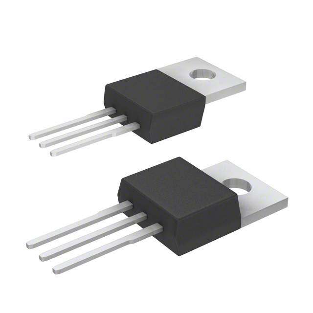
| 描述 | TRANS PNP 6A 40V HI PWR TO220AB两极晶体管 - BJT 6A 40V 65W PNP |
| 产品分类 | 晶体管(BJT) - 单路分离式半导体 |
| 品牌 | ON Semiconductor |
| 产品手册 | |
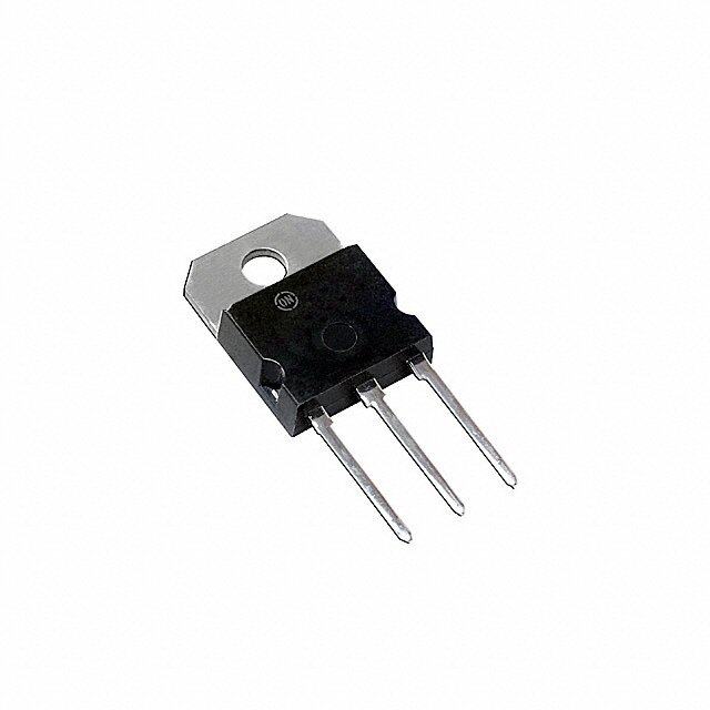
| 产品图片 |
|
| rohs | 符合RoHS无铅 / 符合限制有害物质指令(RoHS)规范要求 |
| 产品系列 | 晶体管,两极晶体管 - BJT,ON Semiconductor TIP42G- |
| 数据手册 | |
| 产品型号 | TIP42G |
| PCN设计/规格 | |
| 不同 Ib、Ic时的 Vce饱和值(最大值) | 1.5V @ 600mA,6A |
| 不同 Ic、Vce 时的DC电流增益(hFE)(最小值) | 15 @ 3A,4V |
| 产品目录页面 | |
| 产品种类 | 两极晶体管 - BJT |
| 供应商器件封装 | TO-220AB |
| 其它名称 | TIP42GOS |
| 功率-最大值 | 2W |
| 包装 | 管件 |
| 发射极-基极电压VEBO | 5 V |
| 商标 | ON Semiconductor |
| 增益带宽产品fT | 3 MHz |
| 安装类型 | 通孔 |
| 安装风格 | Through Hole |
| 封装 | Tube |
| 封装/外壳 | TO-220-3 |
| 封装/箱体 | TO-220-3 |
| 工厂包装数量 | 50 |
| 晶体管极性 | PNP |
| 晶体管类型 | PNP |
| 最大功率耗散 | 65 W |
| 最大工作温度 | + 150 C |
| 最大直流电集电极电流 | 6 A |
| 最小工作温度 | - 65 C |
| 标准包装 | 50 |
| 电压-集射极击穿(最大值) | 40V |
| 电流-集电极(Ic)(最大值) | 6A |
| 电流-集电极截止(最大值) | 700µA |
| 直流集电极/BaseGainhfeMin | 30 |
| 系列 | TIP42 |
| 配置 | Single |
| 集电极—发射极最大电压VCEO | 40 V |
| 集电极—基极电压VCBO | 40 V |
| 集电极—射极饱和电压 | 1.5 V |
| 集电极连续电流 | 6 A |
| 频率-跃迁 | 3MHz |


PDF Datasheet 数据手册内容提取
TIP41G, TIP41AG, TIP41BG, TIP41CG (NPN), TIP42G,(cid:2)TIP42AG, TIP42BG, TIP42CG(cid:2)(PNP) Complementary Silicon Plastic Power Transistors www.onsemi.com 6 AMPERE Designed for use in general purpose amplifier and switching applications. COMPLEMENTARY SILICON POWER TRANSISTORS Features • Epoxy Meets UL 94 V−0 @ 0.125 in 40−60−80−100 VOLTS, • These Devices are Pb−Free and are RoHS Compliant* 65 WATTS MAXIMUM RATINGS PNP NPN Rating Symbol Value Unit COLLECTOR COLLECTOR 2,4 2,4 Collector−Emitter Voltage VCEO Vdc TIP41G, TIP42G 40 TIP41AG, TIP42AG 60 TIP41BG, TIP42BG 80 1 1 TIP41CG, TIP42CG 100 BASE BASE Collector−Base Voltage VCB Vdc TIP41G, TIP42G 40 3 3 TIP41AG, TIP42AG 60 EMITTER EMITTER TIP41BG, TIP42BG 80 TIP41CG, TIP42CG 100 4 Emitter−Base Voltage VEB 5.0 Vdc Collector Current − Continuous IC 6.0 Adc TO−220 CASE 221A Collector Current − Peak ICM 10 Adc STYLE 1 Base Current IB 2.0 Adc 1 2 Total Power Dissipation PD 3 @ TC = 25°C 65 W Derate above 25°C 0.52 W/°C MARKING DIAGRAM Total Power Dissipation PD @ TA = 25°C 2.0 W Derate above 25°C 0.016 W/°C Unclamped Inductive Load Energy E 62.5 mJ (Note1) TIP4xxG Operating and Storage Junction, TJ, Tstg –65 to +150 °C AYWW Temperature Range ESD − Human Body Model HBM 3B V ESD − Machine Model MM C V Stresses exceeding those listed in the Maximum Ratings table may damage the TIP4xx = Device Code device. If any of these limits are exceeded, device functionality should not be xx = 1, 1A, 1B, 1C assumed, damage may occur and reliability may be affected. 2, 2A, 2B, 2C 1. IC = 2.5 A, L = 20 mH, P.R.F. = 10 Hz, VCC = 10 V, RBE = 100 (cid:2). A = Assembly Location Y = Year WW = Work Week G = Pb−Free Package *For additional information on our Pb−Free strategy and soldering details, please download the ONSemiconductor Soldering and Mounting Techniques ORDERING INFORMATION Reference Manual, SOLDERRM/D. See detailed ordering and shipping information on page 6 of this data sheet. © Semiconductor Components Industries, LLC, 2014 1 Publication Order Number: October, 2014 − Rev. 11 TIP41A/D
TIP41G, TIP41AG, TIP41BG, TIP41CG (NPN), TIP42G, TIP42AG, TIP42BG, TIP42CG (PNP) THERMAL CHARACTERISTICS Characteristic Symbol Max Unit Thermal Resistance, Junction−to−Case R(cid:3)JC 1.67 °C/W Thermal Resistance, Junction−to−Ambient R(cid:3)JA 57 °C/W ELECTRICAL CHARACTERISTICS (TC = 25°C unless otherwise noted) Characteristic Symbol Min Max Unit OFF CHARACTERISTICS Collector−Emitter Sustaining Voltage (Note 2) VCEO(sus) Vdc (IC = 30 mAdc, IB = 0) TIP41G, TIP42G 40 − TIP41AG, TIP42AG 60 − TIP41BG, TIP42BG 80 − TIP41CG, TIP42CG 100 − Collector Cutoff Current ICEO mAdc (VCE = 30 Vdc, IB = 0) TIP41G, TIP41AG, TIP42G, TIP42AG − 0.7 (VCE = 60 Vdc, IB = 0) TIP41BG, TIP41CG, TIP42BG, TIP42CG − 0.7 Collector Cutoff Current ICES (cid:4)Adc (VCE = 40 Vdc, VEB = 0) TIP41G, TIP42G − 400 (VCE = 60 Vdc, VEB = 0) TIP41AG, TIP42AG − 400 (VCE = 80 Vdc, VEB = 0) TIP41BG, TIP42BG − 400 (VCE = 100 Vdc, VEB = 0) TIP41CG, TIP42CG − 400 Emitter Cutoff Current (VBE = 5.0 Vdc, IC = 0) IEBO − 1.0 mAdc ON CHARACTERISTICS (Note 2) DC Current Gain hFE − (IC = 0.3 Adc, VCE = 4.0 Vdc) 30 − (IC = 3.0 Adc, VCE = 4.0 Vdc) 15 75 Collector−Emitter Saturation Voltage VCE(sat) Vdc (IC = 6.0 Adc, IB = 600 mAdc) − 1.5 Base−Emitter On Voltage VBE(on) Vdc (IC = 6.0 Adc, VCE = 4.0 Vdc) − 2.0 DYNAMIC CHARACTERISTICS Current−Gain − Bandwidth Product fT MHz (IC = 500 mAdc, VCE = 10 Vdc, ftest = 1.0 MHz) 3.0 − Small−Signal Current Gain hfe − (IC = 0.5 Adc, VCE = 10 Vdc, f = 1.0 kHz) 20 − Product parametric performance is indicated in the Electrical Characteristics for the listed test conditions, unless otherwise noted. Product performance may not be indicated by the Electrical Characteristics if operated under different conditions. 2. Pulse Test: Pulse Width ≤ 300 (cid:4)s, Duty Cycle ≤ 2.0%. www.onsemi.com 2
TIP41G, TIP41AG, TIP41BG, TIP41CG (NPN), TIP42G, TIP42AG, TIP42BG, TIP42CG (PNP) TA TC 4.0 80 S) T AT 3.0 60 W N ( O TI TC A SIP 2.0 40 S DI R WE TA O 1.0 20 P , D P 0 0 0 20 40 60 80 100 120 140 160 T, TEMPERATURE (°C) Figure 1. Power Derating VCC +(cid:4)30 V 25 (cid:4)s RC +11 V SCOPE RB 0 -(cid:4)9.0 V D1 tr, tf ≤ 10 ns DUTY CYCLE = 1.0% -(cid:4)4 V RB and RC VARIED TO OBTAIN DESIRED CURRENT LEVELS D1 MUST BE FAST RECOVERY TYPE, e.g.: (cid:5)(cid:5)1N5825 USED ABOVE IB ≈ 100 mA (cid:5)(cid:5)MSD6100 USED BELOW IB ≈ 100 mA Figure 2. Switching Time Test Circuit 2.0 1.0 TJ = 25°C 0.7 VCC = 30 V 0.5 IC/IB = 10 μE ((cid:2)(cid:3)s) 00..32 tr M TI t, 0.1 0.07 td @ VBE(off) ≈ 5.0 V 0.05 0.03 0.02 0.06 0.1 0.2 0.4 0.6 1.0 2.0 4.0 6.0 IC, COLLECTOR CURRENT (AMP) Figure 3. Turn−On Time www.onsemi.com 3
TIP41G, TIP41AG, TIP41BG, TIP41CG (NPN), TIP42G, TIP42AG, TIP42BG, TIP42CG (PNP) D) E LIZ 1.0 A M 0.7 R D = 0.5 O 0.5 N CE ( 0.3 N 0.2 TA 0.2 S SI 0.1 E ERMAL R000..00.175 0.05 ZRD(cid:3) (cid:3)CJJCCU( tR=) V=1 E.r9(St2) °ARCP(cid:3)/PWJCL YM FAOXR POWER P(pk) T TH0.03 0.02 PULSE TRAIN SHOWN t1 EN READ TIME AT t1 t2 ANSI0.02 0.01 SINGLE PULSE TJ(pk) - TC = P(pk) Z(cid:3)JC(t) DUTY CYCLE, D = t1/t2 R T0.01 r(t), 0.01 0.02 0.05 1.0 0.2 0.5 1.0 2.0 5.0 10 20 50 100 200 500 1.0 k t, TIME (ms) Figure 4. Thermal Response 10 There are two limitations on the power handling ability of 0.5(cid:3)ms a transistor: average junction temperature and second MP)5.0 breakdown. Safe operating area curves indicate IC − VCE A 1.0(cid:3)ms limits of the transistor that must be observed for reliable RENT (23..00 CURVES ATJP =P L1Y5 0B°ECLOW RATED VCEO operation; i.e., the transistor must not be subjected to greater R dissipation than the curves indicate. U SECONDARY BREAKDOWN LTD 5.0(cid:3)ms R C1.0 BONDING WIRE LTD The data of Figure 5 is based on TJ(pk) = 150°C; TC is TO THERMAL LIMITATION @ TC = 25°C variable depending on conditions. Second breakdown pulse EC0.5 (SINGLE PULSE) limits are valid for duty cycles to 10% provided T L J(pk) COL0.3 TIP41, TIP42 ≤ 150°C. TJ(pk) may be calculated from the data in Figure 4. , C0.2 TIP41A, TIP42A At high case temperatures, thermal limitations will reduce I TIP41B, TIP42B the power that can be handled to values less than the TIP41C, TIP42C 0.1 limitations imposed by second breakdown. 5.0 10 20 40 60 80 100 VCE, COLLECTOR-EMITTER VOLTAGE (VOLTS) Figure 5. Active−Region Safe Operating Area 5.0 300 3.0 TJ = 25°C TJ = 25°C 2.0 VCC = 30 V 200 μ(cid:2)(cid:3)s) 10..07 ts IICB1/I B= =IB 120 NCE (pF) Cib E ( 0.5 TA 100 M CI TI A t, 0.3 AP 70 0.2 tf C, C Cob 50 0.1 0.07 0.05 30 0.06 0.1 0.2 0.4 0.6 1.0 2.0 4.0 6.0 0.5 1.0 2.0 3.0 5.0 10 20 30 50 IC, COLLECTOR CURRENT (AMP) VR, REVERSE VOLTAGE (VOLTS) Figure 6. Turn−Off Time Figure 7. Capacitance www.onsemi.com 4
TIP41G, TIP41AG, TIP41BG, TIP41CG (NPN), TIP42G, TIP42AG, TIP42BG, TIP42CG (PNP) 500 S) 2.0 T 300 VCE = 2.0 V VOL TJ = 25°C 200 TJ = 150°C GE ( 1.6 N A GAI 100 OLT RRENT 7500 25°C TTER V 1.2 IC = 1.0 A 2.5 A 5.0 A CU MI DC 30 R-E 0.8 , E 20 -(cid:4)55°C TO F C h E L 0.4 10 OL C 7.0 , E 5.0 VC 0 0.06 0.1 0.2 0.3 0.4 0.6 1.0 2.0 4.0 6.0 10 20 30 50 100 200 300 500 1000 IC, COLLECTOR CURRENT (AMP) IB, BASE CURRENT (mA) Figure 8. DC Current Gain Figure 9. Collector Saturation Region 2.0 +(cid:4)2.5 C) TJ = 25°C °V/+(cid:4)2.0 *APPLIES FOR IC/IB ≤ hFE/4 m 1.6 S (+(cid:4)1.5 T GE (VOLTS) 1.2 OEFFICIEN++(cid:4)(cid:4)10..005 *(cid:4)(cid:3)VC FOR VCE(sat) +(cid:4)25°C to +(cid:4)150°C V, VOLTA 0.8 VBVEB(sEa t@) @ V CICE/ I=B 4=. 01 0V RATURE C--(cid:4)(cid:4)01..50 +-(cid:4)2(cid:4)555°°CC ttoo ++(cid:4)1(cid:4)2550°°CC E 0.4 MP-(cid:4)1.5 (cid:3)VB FOR VBE VCE(sat) @ IC/IB = 10 , TEV-(cid:4)2.0 -(cid:4)55°C to +(cid:4)25°C θ 0 -(cid:4)2.5 0.06 0.1 0.2 0.3 0.4 0.6 1.0 2.0 3.0 4.0 6.0 0.06 0.1 0.2 0.3 0.5 1.0 2.0 3.0 4.0 6.0 IC, COLLECTOR CURRENT (AMP) IC, COLLECTOR CURRENT (AMP) Figure 10. “On” Voltages Figure 11. Temperature Coefficients S) M 103 OH 10(cid:3)M E ( μT ((cid:2)(cid:3)A) 102 VCET =J 3=0 1 V50°C ESISTANC 1.0(cid:3)M IC = 10 x ICES VCE = 30 V REN 101 100°C R R IC ≈ ICES OLLECTOR CUR 1100-01 IC = ICES 25°C L BASE-EMITTE 11000(cid:3)(cid:3)kk IC = 2 x ICES , CIC 10-2 REVERSE FORWARD TERNA 1.0(cid:3)k OBT(TAYINPEICDA FLR ICOEMS FVIAGLUUREES 12) X E 10-3 , E0.1(cid:3)k -(cid:4)0.3 -(cid:4)0.2 -(cid:4)0.1 0 +(cid:4)0.1 +(cid:4)0.2 +(cid:4)0.3 +(cid:4)0.4 +(cid:4)0.5 +(cid:4)0.6 +(cid:4)0.7 RB 20 40 60 80 100 120 140 160 VBE, BASE-EMITTER VOLTAGE (VOLTS) TJ, JUNCTION TEMPERATURE (°C) Figure 12. Collector Cut−Off Region Figure 13. Effects of Base−Emitter Resistance www.onsemi.com 5
TIP41G, TIP41AG, TIP41BG, TIP41CG (NPN), TIP42G, TIP42AG, TIP42BG, TIP42CG (PNP) ORDERING INFORMATION Device Package Shipping TIP41G TO−220 50 Units / Rail (Pb−Free) TIP41AG TO−220 50 Units / Rail (Pb−Free) TIP41BG TO−220 50 Units / Rail (Pb−Free) TIP41CG TO−220 50 Units / Rail (Pb−Free) TIP42G TO−220 50 Units / Rail (Pb−Free) TIP42AG TO−220 50 Units / Rail (Pb−Free) TIP42BG TO−220 50 Units / Rail (Pb−Free) TIP42CG TO−220 50 Units / Rail (Pb−Free) www.onsemi.com 6
TIP41G, TIP41AG, TIP41BG, TIP41CG (NPN), TIP42G, TIP42AG, TIP42BG, TIP42CG (PNP) PACKAGE DIMENSIONS TO−220 CASE 221A−09 ISSUE AH NOTES: 1. DIMENSIONING AND TOLERANCING PER ANSI Y14.5M, 1982. SEATING −T− PLANE 2. CONTROLLING DIMENSION: INCH. 3. DIMENSION Z DEFINES A ZONE WHERE ALL B F C BODY AND LEAD IRREGULARITIES ARE T S ALLOWED. INCHES MILLIMETERS 4 DIM MIN MAX MIN MAX A 0.570 0.620 14.48 15.75 Q A B 0.380 0.415 9.66 10.53 C 0.160 0.190 4.07 4.83 1 2 3 U D 0.025 0.038 0.64 0.96 F 0.142 0.161 3.61 4.09 H G 0.095 0.105 2.42 2.66 H 0.110 0.161 2.80 4.10 K J 0.014 0.024 0.36 0.61 Z K 0.500 0.562 12.70 14.27 L 0.045 0.060 1.15 1.52 N 0.190 0.210 4.83 5.33 L R Q 0.100 0.120 2.54 3.04 R 0.080 0.110 2.04 2.79 V J S 0.045 0.055 1.15 1.39 T 0.235 0.255 5.97 6.47 G U 0.000 0.050 0.00 1.27 D V 0.045 --- 1.15 --- Z --- 0.080 --- 2.04 N STYLE 1: PIN 1. BASE 2. COLLECTOR 3. EMITTER 4. COLLECTOR ON Semiconductor and the are registered trademarks of Semiconductor Components Industries, LLC (SCILLC) or its subsidiaries in the United States and/or other countries. SCILLC owns the rights to a number of patents, trademarks, copyrights, trade secrets, and other intellectual property. A listing of SCILLC’s product/patent coverage may be accessed at www.onsemi.com/site/pdf/Patent−Marking.pdf. SCILLC reserves the right to make changes without further notice to any products herein. SCILLC makes no warranty, representation or guarantee regarding the suitability of its products for any particular purpose, nor does SCILLC assume any liability arising out of the application or use of any product or circuit, and specifically disclaims any and all liability, including without limitation special, consequential or incidental damages. “Typical” parameters which may be provided in SCILLC data sheets and/or specifications can and do vary in different applications and actual performance may vary over time. All operating parameters, including “Typicals” must be validated for each customer application by customer’s technical experts. SCILLC does not convey any license under its patent rights nor the rights of others. SCILLC products are not designed, intended, or authorized for use as components in systems intended for surgical implant into the body, or other applications intended to support or sustain life, or for any other application in which the failure of the SCILLC product could create a situation where personal injury or death may occur. Should Buyer purchase or use SCILLC products for any such unintended or unauthorized application, Buyer shall indemnify and hold SCILLC and its officers, employees, subsidiaries, affiliates, and distributors harmless against all claims, costs, damages, and expenses, and reasonable attorney fees arising out of, directly or indirectly, any claim of personal injury or death associated with such unintended or unauthorized use, even if such claim alleges that SCILLC was negligent regarding the design or manufacture of the part. SCILLC is an Equal Opportunity/Affirmative Action Employer. This literature is subject to all applicable copyright laws and is not for resale in any manner. PUBLICATION ORDERING INFORMATION LITERATURE FULFILLMENT: N. American Technical Support: 800−282−9855 Toll Free ON Semiconductor Website: www.onsemi.com Literature Distribution Center for ON Semiconductor USA/Canada P.O. Box 5163, Denver, Colorado 80217 USA Europe, Middle East and Africa Technical Support: Order Literature: http://www.onsemi.com/orderlit Phone: 303−675−2175 or 800−344−3860 Toll Free USA/Canada Phone: 421 33 790 2910 Fax: 303−675−2176 or 800−344−3867 Toll Free USA/Canada Japan Customer Focus Center For additional information, please contact your local Email: orderlit@onsemi.com Phone: 81−3−5817−1050 Sales Representative www.onsemi.com TIP41A/D 7
Mouser Electronics Authorized Distributor Click to View Pricing, Inventory, Delivery & Lifecycle Information: O N Semiconductor: TIP41AG TIP41BG TIP41CG TIP42AG TIP42BG TIP42CG TIP42G